WO2020017550A1 - 金属ベース基板 - Google Patents
金属ベース基板 Download PDFInfo
- Publication number
- WO2020017550A1 WO2020017550A1 PCT/JP2019/028080 JP2019028080W WO2020017550A1 WO 2020017550 A1 WO2020017550 A1 WO 2020017550A1 JP 2019028080 W JP2019028080 W JP 2019028080W WO 2020017550 A1 WO2020017550 A1 WO 2020017550A1
- Authority
- WO
- WIPO (PCT)
- Prior art keywords
- layer
- circuit layer
- metal base
- purity
- base substrate
- Prior art date
Links
Images

Classifications
-
- H—ELECTRICITY
- H01—ELECTRIC ELEMENTS
- H01L—SEMICONDUCTOR DEVICES NOT COVERED BY CLASS H10
- H01L23/00—Details of semiconductor or other solid state devices
- H01L23/34—Arrangements for cooling, heating, ventilating or temperature compensation ; Temperature sensing arrangements
- H01L23/36—Selection of materials, or shaping, to facilitate cooling or heating, e.g. heatsinks
- H01L23/373—Cooling facilitated by selection of materials for the device or materials for thermal expansion adaptation, e.g. carbon
- H01L23/3735—Laminates or multilayers, e.g. direct bond copper ceramic substrates
-
- B—PERFORMING OPERATIONS; TRANSPORTING
- B32—LAYERED PRODUCTS
- B32B—LAYERED PRODUCTS, i.e. PRODUCTS BUILT-UP OF STRATA OF FLAT OR NON-FLAT, e.g. CELLULAR OR HONEYCOMB, FORM
- B32B27/00—Layered products comprising a layer of synthetic resin
- B32B27/28—Layered products comprising a layer of synthetic resin comprising synthetic resins not wholly covered by any one of the sub-groups B32B27/30 - B32B27/42
- B32B27/281—Layered products comprising a layer of synthetic resin comprising synthetic resins not wholly covered by any one of the sub-groups B32B27/30 - B32B27/42 comprising polyimides
-
- H—ELECTRICITY
- H01—ELECTRIC ELEMENTS
- H01B—CABLES; CONDUCTORS; INSULATORS; SELECTION OF MATERIALS FOR THEIR CONDUCTIVE, INSULATING OR DIELECTRIC PROPERTIES
- H01B5/00—Non-insulated conductors or conductive bodies characterised by their form
- H01B5/14—Non-insulated conductors or conductive bodies characterised by their form comprising conductive layers or films on insulating-supports
-
- H—ELECTRICITY
- H01—ELECTRIC ELEMENTS
- H01L—SEMICONDUCTOR DEVICES NOT COVERED BY CLASS H10
- H01L23/00—Details of semiconductor or other solid state devices
- H01L23/12—Mountings, e.g. non-detachable insulating substrates
-
- H—ELECTRICITY
- H01—ELECTRIC ELEMENTS
- H01L—SEMICONDUCTOR DEVICES NOT COVERED BY CLASS H10
- H01L23/00—Details of semiconductor or other solid state devices
- H01L23/12—Mountings, e.g. non-detachable insulating substrates
- H01L23/14—Mountings, e.g. non-detachable insulating substrates characterised by the material or its electrical properties
- H01L23/142—Metallic substrates having insulating layers
-
- H—ELECTRICITY
- H01—ELECTRIC ELEMENTS
- H01L—SEMICONDUCTOR DEVICES NOT COVERED BY CLASS H10
- H01L23/00—Details of semiconductor or other solid state devices
- H01L23/34—Arrangements for cooling, heating, ventilating or temperature compensation ; Temperature sensing arrangements
- H01L23/36—Selection of materials, or shaping, to facilitate cooling or heating, e.g. heatsinks
- H01L23/373—Cooling facilitated by selection of materials for the device or materials for thermal expansion adaptation, e.g. carbon
- H01L23/3737—Organic materials with or without a thermoconductive filler
-
- H—ELECTRICITY
- H05—ELECTRIC TECHNIQUES NOT OTHERWISE PROVIDED FOR
- H05K—PRINTED CIRCUITS; CASINGS OR CONSTRUCTIONAL DETAILS OF ELECTRIC APPARATUS; MANUFACTURE OF ASSEMBLAGES OF ELECTRICAL COMPONENTS
- H05K1/00—Printed circuits
- H05K1/02—Details
- H05K1/03—Use of materials for the substrate
- H05K1/05—Insulated conductive substrates, e.g. insulated metal substrate
- H05K1/056—Insulated conductive substrates, e.g. insulated metal substrate the metal substrate being covered by an organic insulating layer
-
- H—ELECTRICITY
- H05—ELECTRIC TECHNIQUES NOT OTHERWISE PROVIDED FOR
- H05K—PRINTED CIRCUITS; CASINGS OR CONSTRUCTIONAL DETAILS OF ELECTRIC APPARATUS; MANUFACTURE OF ASSEMBLAGES OF ELECTRICAL COMPONENTS
- H05K1/00—Printed circuits
- H05K1/02—Details
- H05K1/09—Use of materials for the conductive, e.g. metallic pattern
-
- B—PERFORMING OPERATIONS; TRANSPORTING
- B32—LAYERED PRODUCTS
- B32B—LAYERED PRODUCTS, i.e. PRODUCTS BUILT-UP OF STRATA OF FLAT OR NON-FLAT, e.g. CELLULAR OR HONEYCOMB, FORM
- B32B15/00—Layered products comprising a layer of metal
- B32B15/04—Layered products comprising a layer of metal comprising metal as the main or only constituent of a layer, which is next to another layer of the same or of a different material
- B32B15/08—Layered products comprising a layer of metal comprising metal as the main or only constituent of a layer, which is next to another layer of the same or of a different material of synthetic resin
-
- B—PERFORMING OPERATIONS; TRANSPORTING
- B32—LAYERED PRODUCTS
- B32B—LAYERED PRODUCTS, i.e. PRODUCTS BUILT-UP OF STRATA OF FLAT OR NON-FLAT, e.g. CELLULAR OR HONEYCOMB, FORM
- B32B15/00—Layered products comprising a layer of metal
- B32B15/20—Layered products comprising a layer of metal comprising aluminium or copper
-
- B—PERFORMING OPERATIONS; TRANSPORTING
- B32—LAYERED PRODUCTS
- B32B—LAYERED PRODUCTS, i.e. PRODUCTS BUILT-UP OF STRATA OF FLAT OR NON-FLAT, e.g. CELLULAR OR HONEYCOMB, FORM
- B32B2250/00—Layers arrangement
- B32B2250/03—3 layers
-
- B—PERFORMING OPERATIONS; TRANSPORTING
- B32—LAYERED PRODUCTS
- B32B—LAYERED PRODUCTS, i.e. PRODUCTS BUILT-UP OF STRATA OF FLAT OR NON-FLAT, e.g. CELLULAR OR HONEYCOMB, FORM
- B32B2264/00—Composition or properties of particles which form a particulate layer or are present as additives
- B32B2264/10—Inorganic particles
- B32B2264/107—Ceramic
-
- B—PERFORMING OPERATIONS; TRANSPORTING
- B32—LAYERED PRODUCTS
- B32B—LAYERED PRODUCTS, i.e. PRODUCTS BUILT-UP OF STRATA OF FLAT OR NON-FLAT, e.g. CELLULAR OR HONEYCOMB, FORM
- B32B2307/00—Properties of the layers or laminate
- B32B2307/20—Properties of the layers or laminate having particular electrical or magnetic properties, e.g. piezoelectric
- B32B2307/206—Insulating
-
- B—PERFORMING OPERATIONS; TRANSPORTING
- B32—LAYERED PRODUCTS
- B32B—LAYERED PRODUCTS, i.e. PRODUCTS BUILT-UP OF STRATA OF FLAT OR NON-FLAT, e.g. CELLULAR OR HONEYCOMB, FORM
- B32B2307/00—Properties of the layers or laminate
- B32B2307/30—Properties of the layers or laminate having particular thermal properties
- B32B2307/302—Conductive
-
- B—PERFORMING OPERATIONS; TRANSPORTING
- B32—LAYERED PRODUCTS
- B32B—LAYERED PRODUCTS, i.e. PRODUCTS BUILT-UP OF STRATA OF FLAT OR NON-FLAT, e.g. CELLULAR OR HONEYCOMB, FORM
- B32B2457/00—Electrical equipment
- B32B2457/08—PCBs, i.e. printed circuit boards
-
- H—ELECTRICITY
- H05—ELECTRIC TECHNIQUES NOT OTHERWISE PROVIDED FOR
- H05K—PRINTED CIRCUITS; CASINGS OR CONSTRUCTIONAL DETAILS OF ELECTRIC APPARATUS; MANUFACTURE OF ASSEMBLAGES OF ELECTRICAL COMPONENTS
- H05K2201/00—Indexing scheme relating to printed circuits covered by H05K1/00
- H05K2201/02—Fillers; Particles; Fibers; Reinforcement materials
- H05K2201/0203—Fillers and particles
- H05K2201/0206—Materials
- H05K2201/0209—Inorganic, non-metallic particles
Definitions
- the present invention relates to a metal base substrate.
- Priority is claimed on Japanese Patent Application No. 2018-134789, filed on July 18, 2018, the content of which is incorporated herein by reference.
- a metal base substrate is known as one of substrates for mounting electronic components such as semiconductor elements.
- the metal base substrate is a laminate in which a metal substrate, an insulating layer, and a circuit layer are laminated in this order.
- the electronic component is mounted on the circuit layer via solder.
- heat generated in the electronic component is transmitted to the metal substrate via the insulating layer, and is radiated to the outside from the metal substrate.
- the insulating layer of the metal base substrate is generally formed of an insulating resin composition containing a resin having excellent insulating properties and ceramic particles (thermally conductive filler) having excellent thermal conductivity.
- a resin for the insulating layer a polyimide resin, a polyamideimide resin, or a silicone resin is used.
- Patent Document 1 discloses a metal-clad laminate using a polyimide resin layer containing a thermally conductive filler in a range of 40 to 80 vol% as an insulating layer.
- Patent Document 2 discloses that the resin forming the insulating layer is a silicone resin having a polydimethylsiloxane skeleton, the inorganic filler in the insulating layer is 45 to 60% by volume, and 25% by mass or more of the inorganic filler.
- the substrate is crystalline silica.
- the metal-clad laminate as described in Patent Document 1 generally has a large coefficient of thermal expansion, and an electronic component usually made of ceramic has a low coefficient of thermal expansion.
- an electronic component usually made of ceramic has a low coefficient of thermal expansion.
- the silicone resin described in Patent Document 2 has lower elasticity than polyimide resin and polyamideimide resin.
- the insulating layer of the metal base substrate contains a thermally conductive filler, the elasticity of the insulating layer is lower than that of the silicone resin alone. For this reason, it is difficult to sufficiently reduce the stress applied to the solder joining the electronic component and the metal base substrate by the thermal cycle only by using the silicone resin as the resin for the insulating layer.
- the present invention has been made in view of the above-described circumstances, and has as its object to provide a metal base in which solder cracks are unlikely to occur even when a thermal cycle is applied in a state where electronic components are mounted via solder. It is to provide a circuit board.
- a metal base substrate of the present invention is a metal base substrate in which a metal substrate, an insulating layer, and a circuit layer are stacked in this order, wherein the insulating layer includes a resin.
- the circuit layer has a thickness in the range of 10 ⁇ m or more and 1000 ⁇ m or less, and the average crystal grain size in units of ⁇ m and the purity in units of mass% satisfy the following formula (1). It is characterized by satisfaction. Average crystal grain size / (100-purity)> 5 (1)
- the circuit layer is easily deformed because the film thickness is in the range of 10 ⁇ m or more and 1000 ⁇ m or less and the average crystal grain size and the purity satisfy the above formula (1). For this reason, when the thermal cycle is applied, the stress applied to the solder can be reduced by deforming the circuit layer, so that the occurrence of solder cracks can be suppressed.
- the average crystal grain size and the purity of the circuit layer satisfy the following expression (2).
- the circuit layer satisfies the above expression (2) and is more easily deformed, so that the stress applied to the solder can be more reliably reduced.
- the circuit layer has the average crystal grain size of 0.3 ⁇ m or more.
- the average crystal grain size of the circuit layer is as large as 0.3 ⁇ m or more, the metal crystal grains constituting the circuit layer easily slide. Therefore, since the circuit layer is more easily deformed, the stress applied to the solder can be more reliably reduced.
- the purity of the circuit layer is preferably 99.99% by mass or more.
- the purity of the circuit layer is as high as 99.99% by mass or more and the content of impurities is reduced, the metal crystal grains are easily slipped. Therefore, since the circuit layer is more easily deformed, the stress applied to the solder can be more reliably reduced.
- the circuit layer is made of aluminum.
- the average crystal grain size of aluminum tends to increase by heat treatment, the effect of suppressing the occurrence of solder cracks by the circuit layer can be relatively easily increased by heat treatment.
- the present invention it is possible to provide a metal base substrate in which solder cracks are unlikely to occur even when a thermal cycle is applied in a state where electronic components are mounted via solder.
- FIG. 1 is a schematic sectional view of a module using a metal base substrate according to one embodiment of the present invention.
- FIG. 1 is a schematic sectional view of a module using a metal base substrate according to one embodiment of the present invention.
- the module 1 includes a metal base substrate 2 and an electronic component 3 mounted on the metal base substrate 2.
- the metal base substrate 2 is a laminate in which a metal substrate 10, an insulating layer 20, an adhesion layer 30, and a circuit layer 40 are laminated in this order.
- the circuit layer 40 is formed in a circuit pattern.
- the electronic component 3 is joined via the solder 4 on the circuit layer 40 formed in the circuit pattern.
- the metal substrate 10 is a member serving as a base of the metal base substrate 2.
- a copper plate, an aluminum plate, and a laminate thereof can be used as the metal substrate 10.
- the insulating layer 20 is a layer for insulating the metal substrate 10 and the circuit layer 40.
- the insulating layer 20 is formed from an insulating resin composition including an insulating resin 21 and ceramic particles 22 (thermally conductive filler).
- an insulating resin composition including an insulating resin 21 having a high insulating property and ceramic particles 22 having a high thermal conductivity By forming the insulating layer 20 from an insulating resin composition including an insulating resin 21 having a high insulating property and ceramic particles 22 having a high thermal conductivity, the insulating layer 20 is maintained from the circuit layer 40 to the metal substrate while maintaining the insulating property. Thermal resistance of the entire metal base substrate 2 up to 10 can be further reduced.
- the insulating resin 21 is preferably a polyimide resin or a polyamideimide resin, or a mixture thereof. Since the polyimide resin and the polyamide-imide resin have an imide bond, they have excellent heat resistance and mechanical properties.
- silica (silicon dioxide) particles, alumina (aluminum oxide) particles, boron nitride (BN) particles, titanium oxide particles, alumina-doped silica particles, alumina hydrate particles, aluminum nitride particles, and the like can be used. It can.
- the ceramic particles 22 one kind may be used alone, or two or more kinds may be used in combination. Among these ceramic particles, alumina particles are preferred because of their high thermal conductivity.
- the form of the ceramic particles 22 is not particularly limited, but is preferably agglomerated particles of fine ceramic particles or single-crystal ceramic particles.
- Agglomerated particles of fine ceramic particles may be agglomerates in which primary particles are relatively weakly connected or aggregates in which primary particles are relatively strongly connected. Further, the aggregated particles may form a particle aggregate further aggregated. Since the primary particles of the ceramic particles 22 form aggregated particles and are dispersed in the insulating layer 20, a network is formed by mutual contact between the ceramic particles 22 and heat is conducted between the primary particles of the ceramic particles 22. And the thermal conductivity of the insulating layer 20 is improved.
- aggregated particles of fine ceramic particles include AE50, AE130, AE200, AE300, AE380, AE90E (all manufactured by Nippon Aerosil Co., Ltd.), T400 (manufactured by Wacker), SFP-20M (manufactured by Denka Corporation) ), Alumina particles such as Alu65 (manufactured by Nippon Aerosil Co., Ltd.), AA-04 (manufactured by Sumitomo Chemical Co., Ltd.), boron nitride particles such as AP-170S (manufactured by Maruka), AEROXIDE (R) TiO2 @ P90 Titanium oxide particles such as (manufactured by Nippon Aerosil Co., Ltd.), alumina-doped silica particles such as MOX170 (manufactured by Nippon Aerosil Co., Ltd.), and alumina hydrate particles manufactured by Sasol can be used.
- Alumina particles such as Alu65 (
- the single-crystal ceramic particles are preferably ⁇ -alumina single crystal particles having a crystal structure of ⁇ -alumina ( ⁇ Al 2 O 3 ).
- ⁇ -alumina single crystal particles include Advanced Alumina (AA) series AA-03, AA-04, AA-05, AA-07 and AA-1.5 sold by Sumitomo Chemical Co., Ltd. Can be used.
- the content of the ceramic particles 22 in the insulating layer 20 is preferably in the range of 5% by volume to 60% by volume. If the content of the ceramic particles 22 is too small, the thermal conductivity of the insulating layer 20 may not be sufficiently improved. On the other hand, if the content of the ceramic particles 22 is too large, the content of the insulating resin 21 may be relatively reduced, and the shape of the insulating layer 20 may not be stably maintained. In addition, the ceramic particles 22 tend to form excessively large aggregated particles, and the surface roughness Ra of the insulating layer 20 on the side of the adhesive layer 30 may increase. In order to reliably improve the thermal conductivity of the insulating layer 20, the content of the ceramic particles 22 is preferably 10% by volume or more.
- the content of the ceramic particles 22 is particularly preferably 50% by volume or less.
- the thickness of the insulating layer 20 is not particularly limited, but is preferably in a range of 1 ⁇ m to 200 ⁇ m, and particularly preferably in a range of 3 ⁇ m to 100 ⁇ m.
- the adhesion layer 30 is a layer for improving the adhesion between the insulating layer 20 and the circuit layer 40.
- the adhesion layer 30 preferably has a low Young's modulus and a high adhesion between the insulating layer 20 and the circuit layer 40.
- the Young's modulus of the adhesion layer 30 at 25 ° C. is preferably 5 GPa or less, and particularly preferably in the range of 0.01 GPa or more and 3 GPa or less.
- the adhesion layer 30 is preferably made of a resin.
- a silicone resin an epoxy resin, a polyamideimide resin, or a polyimide resin can be used.
- the silicone resin includes a modified silicone resin into which various organic groups have been introduced.
- modified silicone resins include polyimide-modified silicone resins, polyester-modified silicone resins, urethane-modified silicone resins, acryl-modified silicone resins, olefin-modified silicone resins, ether-modified silicone resins, alcohol-modified silicone resins, fluorine-modified silicone resins, and amino-modified silicone resins.
- examples thereof include silicone resins, mercapto-modified silicone resins, and carboxy-modified silicone resins.
- the epoxy resin examples include a bisphenol A type epoxy resin, a bisphenol F type epoxy resin, a novolak type epoxy resin, an aliphatic type epoxy resin, and a glycidylamine type epoxy resin. These resins may be used alone or in a combination of two or more.
- the adhesive layer 30 may have a thermally conductive filler dispersed therein to improve thermal conductivity.
- Ceramic particles can be used as the thermally conductive filler. Examples of the ceramic particles include silica (silicon dioxide) particles, alumina (aluminum oxide) particles, boron nitride particles, titanium oxide particles, alumina-doped silica particles, alumina hydrate particles, and aluminum nitride particles.
- the content of the thermally conductive filler in the adhesive layer 30 is preferably in the range of 5% by volume to 60% by volume, and particularly preferably in the range of 10% by volume to 50% by volume.
- the thickness of the adhesion layer 30 is not particularly limited, but is preferably in the range of 0.1 ⁇ m to 20 ⁇ m, and particularly preferably in the range of 0.5 ⁇ m to 5 ⁇ m.
- the circuit layer 40 is configured such that the average crystal grain size in units of ⁇ m and the purity in units of mass% satisfy the following expression (1). Average crystal grain size / (100-purity)> 5 (1)
- the average crystal grain size and the purity preferably satisfy the following expression (2), and particularly preferably satisfy the following expression (3).
- the average crystal grain size of the circuit layer 40 is preferably 0.3 ⁇ m or more, more preferably 1.0 ⁇ m or more, and 20 ⁇ m or more and 1000 ⁇ m or less. It is particularly preferable that the ratio is in the range of When the crystal grain size is 0.3 ⁇ m or less, work hardening is apt to occur, and cracks are easily formed in the solder.
- the average crystal grain size of the circuit layer 40 is a value measured by an EBSD method (electron beam backscatter diffraction analysis).
- the purity of the circuit layer 40 is preferably 99% by mass or more, more preferably 99.99% by mass or more, and 99.999% by mass. It is particularly preferable that the above is satisfied. Note that the purity of the circuit layer 40 is a value measured by the difference number method.
- the difference number method is a method in which the content of an impurity element in a sample is measured, and a value obtained by subtracting the content of the impurity element from 100% by mass is used as the purity of the sample.
- the content of the impurity element is measured by an ICP-MS method, and the impurity element to be measured is an element contained in the sample at 0.01 ppm by mass or more.
- the material of the circuit layer 40 aluminum, copper, silver, gold, tin, iron, nickel, chromium, molybdenum, tungsten, palladium, titanium, zinc, and alloys of these metals can be used. Among these metals, aluminum and copper are preferred, and aluminum is particularly preferred.
- the thickness of the circuit layer 40 is in the range of 10 ⁇ m to 1000 ⁇ m, preferably in the range of 20 ⁇ m to 100 ⁇ m. If the thickness of the circuit layer 40 is too thin, the thermal resistance may increase. On the other hand, if the thickness of the circuit layer 40 is too large, it may be difficult to form a circuit pattern by etching. If the thickness of the circuit layer 40 is too large, the thermal stress applied to the circuit layer 40 increases due to the coefficient of thermal expansion of each material constituting the module 1, and the insulating layer 20 during the thermal cycle. And the circuit layer 40 may be easily separated.
- Examples of the electronic component 3 mounted on the circuit layer 40 include, but are not particularly limited to, a semiconductor element, a resistor, a capacitor, and a crystal oscillator.
- Examples of the semiconductor element include a MOSFET (Metal-oxide-semiconductor field effect transistor), an IGBT (Insulated Gate Bipolar Transistor), an LSI (Large Scale Integration), an LED (LED), a LED (Chip-LED), an LED (Chip-LED), an LED (Chip-LED), an LED (Chip-LED), an LED (Chip-LED), an LED (Chip-LED), and a LED-Chip (LED-Chip) Size @ Package).
- the metal base substrate 2 of the present embodiment is manufactured, for example, by a method in which an insulating layer 20 and an adhesion layer 30 are laminated on a metal substrate 10 in this order, and then a circuit layer 40 is adhered on the adhesion layer 30. can do.
- a coating method or an electrodeposition method can be used.
- a coating liquid for forming an insulating layer containing the insulating resin 21, the ceramic particles 22, and a solvent is applied to the surface of the metal substrate 10 to form a coating layer, and then the coating layer is heated and dried.
- the insulating layer 20 is formed on the metal substrate 10.
- a method for applying the coating liquid for forming an insulating layer on the surface of the metal substrate 10 include spin coating, bar coating, knife coating, roll coating, blade coating, die coating, gravure coating, and dip coating. Etc. can be used.
- the electrodeposition method involves immersing a metal substrate 10 and an electrode in an electrodeposition liquid in which insulating resin particles having electric charge and ceramic particles are dispersed, and applying a DC voltage between the metal substrate 10 and the electrode.
- the insulating resin particles and the ceramic particles are electrodeposited on the surface of the metal substrate 10 to form an electrodeposition layer, and then the electrodeposition layer is heated and dried to form the insulating layer 20 on the metal substrate 10.
- the electrodeposition liquid can be prepared, for example, by adding a poor solvent for the insulating resin to an insulating resin solution containing ceramic particles to precipitate the insulating resin.
- the poor solvent for the insulating resin for example, water can be used.
- a coating method can be used.
- the adhesion layer 30 is formed by applying a coating liquid for forming an adhesion layer containing a resin for forming the adhesion layer, a solvent, and a heat conductive filler added as necessary to the surface of the insulating layer 20 to form a coating layer. Then, the coating layer can be formed by heating and drying. Examples of a method for applying the coating solution for forming the adhesion layer on the surface of the insulating layer 20 include spin coating, bar coating, knife coating, roll coating, blade coating, die coating, gravure coating, dip coating, and the like. Can be used.
- the circuit layer 40 can be attached by laminating the circuit layer 40 on the adhesion layer 30 and then heating the circuit layer 40 while applying pressure.
- the heating is preferably performed in a non-oxidizing atmosphere (for example, in a nitrogen atmosphere or in a vacuum) so that the circuit layer 40 is not oxidized.
- the average crystal grain size of the circuit layer 40 can be adjusted by, for example, heat treatment.
- the average crystal grain size of aluminum is increased by heat treatment, and aluminum is easily deformed.
- the heat treatment is preferably performed at a temperature of 200 ° C. or more and 500 ° C. or less.
- the heat treatment time varies depending on the heating temperature, but is usually in the range of 5 minutes to 500 minutes.
- the circuit layer 40 has a film thickness in the range of 10 ⁇ m or more and 1000 ⁇ m or less, and the average crystal grain size and the purity are calculated by the above formula ( Since 1) is satisfied, it is easily deformed. For this reason, when the cooling / heating cycle is applied, the stress applied to the solder can be reduced by deforming the circuit layer 40, so that the occurrence of solder cracks can be suppressed.
- the circuit layer when the average crystal grain size and the purity satisfy the above formula (2), particularly preferably the formula (3), the circuit layer is more easily deformed. Can be more reliably alleviated.
- the metal base substrate 2 of the present embodiment when the average crystal grain size of the circuit layer 40 is 0.3 ⁇ m or more, the metal crystal grains constituting the circuit layer 40 easily slide. Therefore, since the circuit layer 40 is more easily deformed, the stress applied to the solder can be more reliably reduced.
- the purity of the circuit layer is 99.99% by mass or more, the purity is high and the content of impurities is low, so that the metal crystal grains easily slide. Therefore, since the circuit layer 40 is more easily deformed, the stress applied to the solder can be more reliably reduced.
- the effect of suppressing the occurrence of solder cracks by the circuit layer 40 can be relatively easily increased by heat treatment.
- the present invention is not limited thereto, and can be appropriately changed without departing from the technical idea of the present invention.
- the configuration in which the adhesion layer 30 is provided between the insulating layer 20 and the circuit layer 40 has been described, but the present invention is not limited to this. If the insulating layer 20 alone can sufficiently secure the adhesion to the circuit layer 40, the adhesive layer 30 may not be provided. Further, the order of the insulating layer 20 and the adhesion layer 30 may be reversed.
- a laminated body in which the circuit layer 40, the insulating layer 20, and the adhesion layer 30 are laminated in this order is prepared, and the adhesion layer 30 of the laminated body and the metal substrate 10 are pressure-bonded by thermocompression to form a metal base substrate. Can be manufactured.
- Example 1 of the present invention A separable flask having a capacity of 300 mL was charged with 4,4′-diaminodiphenyl ether and NMP (N-methyl-2-pyrrolidone). The amount of NMP was adjusted so that the concentration of the obtained polyamic acid was 40% by mass. After stirring at room temperature to completely dissolve 4,4′-diaminodiphenyl ether, a predetermined amount of tetracarboxylic dianhydride was added little by little so that the internal temperature did not exceed 30 ° C. Thereafter, stirring was continued for 16 hours under a nitrogen atmosphere to prepare a polyamic acid (polyimide precursor) solution.
- NMP N-methyl-2-pyrrolidone
- Alumina particles (average particle diameter: 0.5 ⁇ m) were prepared as ceramic particles (thermally conductive filler). 1.0 g of the prepared alumina particles and 10 g of NMP were mixed and subjected to ultrasonic treatment for 30 minutes to prepare an alumina particle dispersion.
- the polyamic acid solution and the alumina particle dispersion liquid prepared as described above are mixed so that the content of alumina particles in a solid (insulating layer) generated by heating becomes 30% by volume, and then, the mixture is mixed with NMP.
- the mixture was diluted so that the concentration of the polyamic acid in the mixture was 5% by mass.
- the obtained mixture was subjected to dispersion treatment by repeating 10 times of high-pressure injection treatment at a pressure of 50 MPa using Starburst manufactured by Sugino Machine Co., Ltd. to obtain an alumina particle-dispersed polyamic acid solution (coating solution for forming an insulating layer). ) was prepared.
- a coating solution for forming an insulating layer is applied to a surface of a copper substrate having a thickness of 0.3 mm and a size of 30 mm ⁇ 20 mm by a bar coating method so that the thickness of the insulating layer formed by heating is 10 ⁇ m.
- a layer was formed.
- the copper substrate on which the coating layer for forming the insulating layer was formed was placed on a hot plate, and the temperature was raised from room temperature to 60 ° C. at 3 ° C./min. And heated at 120 ° C. for 100 minutes to dry the coating layer for forming an insulating layer. Thereafter, the copper substrate was heated at 250 ° C. for 1 minute and at 400 ° C. for 1 minute to produce a copper substrate with an insulating layer.
- Polyamide imide (elastic modulus: 2 GPa) and NMP were mixed at a mass ratio of 1: 6, and the polyamide imide was dissolved to prepare a polyamide imide solution (coating solution for forming an adhesion layer).
- a coating solution for forming an adhesion layer is applied on the insulating layer of the copper substrate with an insulating layer by spin coating so that the thickness of the adhesion layer formed by heating becomes 1 ⁇ m. A layer was formed.
- the copper substrate with the insulating layer on which the coating layer for forming the adhesion layer is formed is heated, the coating layer for forming the adhesion layer is dried, and the adhesion layer is formed on the insulating layer, and the copper substrate and the insulating layer are adhered to each other.
- a laminate in which the layers were laminated in this order was obtained.
- Aluminum foil (film thickness: 40 ⁇ m, size: 30 mm ⁇ 20 mm) was prepared. This aluminum foil had a purity of 99.999431% by mass, an average crystal grain size of 0.2 ⁇ m, and an average crystal grain size / (100 ⁇ purity) of 351. The purity and the average crystal grain size of the aluminum foil were measured by the following methods.
- the aluminum foil was dissolved with an acid, and the obtained aluminum was measured for the content of impurity elements in the solution by an ICP-MS method.
- the total content of the impurity elements in the aluminum foil was determined from the obtained impurity element content, and the value obtained by subtracting the total content of the impurity elements from 100% by mass was defined as the purity of the aluminum foil.
- the impurity elements are Na, Mg, Si, P, K, Ca, Ti, V, Cr, Mn, Fe, Co, Ni, Cu, Zn, Ga, Ge, Nb, Mo, Ru, Pd, Ag, In, Sn, Sb, Ba, Hf, W, Pt, Au, Pb, and Bi were used.
- Example 2 Comparative Examples 1 to 3
- the aluminum foil used had a film thickness, purity, average grain size, and average grain size / (100-purity) having the values shown in Table 1 below.
- a metal base substrate was manufactured.
- the aluminum foil was subjected to a heat treatment at a temperature of 300.degree. / (100-purity) was adjusted.
- the metal base substrates of Examples 1 to 23 of the present invention in which the average crystal grain size and the purity of the circuit layer (aluminum foil) satisfy the above formula (1) are the same as those of Comparative Examples 1 to 3 not satisfying the above formula (1).
- the crack length of the solder layer after applying the thermal cycle was shorter than that of the metal base substrate of No. 2. This is considered to be because in the metal base substrates of Examples 1 to 23 of the present invention, the stress applied to the solder layer was relaxed due to the deformation of the circuit layer during the application of the thermal cycle.
- Example 2 of the present invention in which the average crystal grain size and the purity of the circuit layer satisfy the above expression (2) the average crystal grain size is 0.3 ⁇ m or more, and the purity is 99.99% by mass or more.
- the crack length of the solder layer after the application of the thermal cycle was significantly reduced to 0.2 ⁇ m or less. Further, in the metal base substrate of Comparative Example 3 in which the thickness of the circuit layer (aluminum foil) exceeded the range of the present invention, the insulating layer and the circuit layer were separated during the thermal cycle.
- Inventive Example 1 except that a copper foil having a film thickness, purity, average crystal grain size, and average crystal grain size / (100-purity) having the values shown in Table 2 below was used instead of the aluminum foil. Similarly, a metal base substrate was prepared, and the crack length of the solder layer after the application of the thermal cycle was measured. The average crystal grain size and average crystal grain size / (100-purity) of the copper foil were adjusted by heat treatment at a temperature of 300 ° C. for a heat treatment time shown in Table 2 below.
- the purity of the copper foil was determined by changing the impurity elements to Na, Mg, Si, Al, P, K, Ca, Ti, V, Cr, Mn, Fe, Co, Ni, Zn, Ga, Ge, Nb, Mo, The measurement was performed in the same manner as the purity of the aluminum foil, except that Ru, Pd, Ag, In, Sn, Sb, Ba, Hf, W, Pt, Au, Pb, and Bi were used.
- the average crystal grain size of the copper foil was measured in the same manner as the average crystal grain size of the aluminum foil.
- the metal base substrates of Examples 24 to 26 of the present invention in which the average crystal grain size and the purity of the circuit layer satisfy the above formula (1)
- the crack length of the solder layer after the application of the thermal cycle was shorter than that of the metal base substrate of Comparative Example 4 not satisfying (1).
- Example 25 of the present invention in which the average crystal grain size and the purity of the circuit layer satisfy the above formula (2) the average crystal grain size is 0.3 ⁇ m or more, and the purity is 99.99% by mass or more.
- the crack length of the solder layer after the application of the thermal cycle was significantly shortened to 0.2 ⁇ m or less.
Landscapes
- Engineering & Computer Science (AREA)
- Microelectronics & Electronic Packaging (AREA)
- Computer Hardware Design (AREA)
- Power Engineering (AREA)
- Condensed Matter Physics & Semiconductors (AREA)
- General Physics & Mathematics (AREA)
- Physics & Mathematics (AREA)
- Chemical & Material Sciences (AREA)
- Materials Engineering (AREA)
- Ceramic Engineering (AREA)
- Insulated Metal Substrates For Printed Circuits (AREA)
- Laminated Bodies (AREA)
- Parts Printed On Printed Circuit Boards (AREA)
- Electric Connection Of Electric Components To Printed Circuits (AREA)
- Cooling Or The Like Of Semiconductors Or Solid State Devices (AREA)
Abstract
金属基板(10)と、絶縁層(20)と、回路層(40)とがこの順で積層された金属ベース基板(2)であって、前記絶縁層(20)は、樹脂を含み、前記回路層(40)は、膜厚が10μm以上1000μm以下の範囲内にあって、単位がμmで表される平均結晶粒径と単位が質量%で表される純度とが下記の式(1)を満足する金属ベース基板(2)。 平均結晶粒径/(100-純度)>5 (1)
Description
本発明は、金属ベース基板に関するものである。
本願は、2018年7月18日に、日本に出願された特願2018-134789号に基づき優先権を主張し、その内容をここに援用する。
本願は、2018年7月18日に、日本に出願された特願2018-134789号に基づき優先権を主張し、その内容をここに援用する。
半導体素子などの電子部品を実装するための基板の一つとして、金属ベース基板が知られている。金属ベース基板は、金属基板と、絶縁層と、回路層とがこの順で積層された積層体である。電子部品は、回路層の上に、はんだを介して実装される。このような構成とされた金属ベース基板では、電子部品にて発生した熱は、絶縁層を介して金属基板に伝達され、金属基板から外部に放熱される。
金属ベース基板の絶縁層は、一般に絶縁性に優れる樹脂と、熱伝導率に優れるセラミック粒子(熱伝導性フィラー)とを含む絶縁性樹脂組成物から形成されている。絶縁層用の樹脂としては、ポリイミド樹脂やポリアミドイミド樹脂、シリコーン樹脂が用いられている。例えば、特許文献1には、絶縁層として、熱伝導性フィラーを40~80vol%の範囲内で含有するポリイミド樹脂層を用いた金属張積層体が開示されている。また、特許文献2には、絶縁層を形成する樹脂がポリジメチルシロキサン骨格からなるシリコーン樹脂であり、絶縁層中の無機充填材が45~60体積%であり、無機充填材の25質量%以上が結晶性シリカである回路基板が開示されている。
ところで、特許文献1に記載されているような金属張積層体は一般に熱膨張率が大きく、通常セラミックからなる電子部品は熱膨張率が低い。金属張積層体と電子部品との熱膨張率の差が大きくなると、電子部品のオン/オフや外部環境による冷熱サイクルによって、電子部品と金属ベース基板とを接合しているはんだに付与される応力が大きくなり、はんだクラックが発生しやすくなるという問題があった。
一方、特許文献2に記載されているシリコーン樹脂は、ポリイミド樹脂やポリアミドイミド樹脂と比較すると弾性が低い。しかしながら、金属ベース基板の絶縁層には、熱伝導性フィラーが含まれているため、絶縁層の弾性はシリコーン樹脂単体と比較して低下する。このため、絶縁層用の樹脂としてシリコーン樹脂を用いることだけでは、冷熱サイクルによって、電子部品と金属ベース基板とを接合しているはんだに付与される応力を十分に低減させることは難しい。
本発明は、前述した事情に鑑みてなされたものであって、その目的は、はんだを介して電子部品を実装した状態で、冷熱サイクルを付与しても、はんだクラックの発生が起こりにくい金属ベース回路基板を提供することにある。
上記の課題を解決するために、本発明の金属ベース基板は、金属基板と、絶縁層と、回路層とがこの順で積層された金属ベース基板であって、前記絶縁層は、樹脂を含み、前記回路層は、膜厚が10μm以上1000μm以下の範囲内にあって、単位がμmで表される平均結晶粒径と単位が質量%で表される純度とが下記の式(1)を満足することを特徴としている。
平均結晶粒径/(100-純度)>5 (1)
平均結晶粒径/(100-純度)>5 (1)
本発明の金属ベース基板によれば、回路層は、膜厚が10μm以上1000μm以下の範囲内にあって、平均結晶粒径と純度が上記の式(1)を満足するので、変形しやすい。このため、冷熱サイクルが付与された場合には、回路層が変形することによって、はんだに付与される応力を緩和することができるので、はんだクラックの発生を抑制することができる。
ここで、本発明の金属ベース基板において、前記回路層は、前記平均結晶粒径と前記純度とが下記の式(2)を満足することが好ましい。
平均結晶粒径/(100-純度)>20 (2)
この場合、回路層が、上記の式(2)を満足し、より変形しやすくなるので、はんだに付与される応力をより確実に緩和することができる。
平均結晶粒径/(100-純度)>20 (2)
この場合、回路層が、上記の式(2)を満足し、より変形しやすくなるので、はんだに付与される応力をより確実に緩和することができる。
また、本発明の金属ベース基板において、前記回路層は、前記平均結晶粒径が0.3μm以上であることが好ましい。
この場合、回路層は、平均結晶粒径が0.3μm以上と大きいので、回路層を構成する金属結晶粒同士がすべりやすくなる。よって、回路層が、より変形しやすくなるので、はんだに付与される応力をより確実に緩和することができる。
この場合、回路層は、平均結晶粒径が0.3μm以上と大きいので、回路層を構成する金属結晶粒同士がすべりやすくなる。よって、回路層が、より変形しやすくなるので、はんだに付与される応力をより確実に緩和することができる。
また、本発明の金属ベース基板において、前記回路層は、前記純度が99.99質量%以上であることが好ましい。
この場合、回路層は純度が99.99質量%以上と高く、不純物の含有量が少なくなるので、金属結晶粒同士がすべりやすくなる。よって、回路層が、より変形しやすくなるので、はんだに付与される応力をより確実に緩和することができる。
この場合、回路層は純度が99.99質量%以上と高く、不純物の含有量が少なくなるので、金属結晶粒同士がすべりやすくなる。よって、回路層が、より変形しやすくなるので、はんだに付与される応力をより確実に緩和することができる。
また、本発明の金属ベース基板において、前記回路層は、アルミニウムからなることが好ましい。
この場合、アルミニウムは熱処理によって平均結晶粒径が増大しやすいため、回路層によるはんだクラックの発生を抑制する効果を熱処理により比較的容易に高くすることができる。
この場合、アルミニウムは熱処理によって平均結晶粒径が増大しやすいため、回路層によるはんだクラックの発生を抑制する効果を熱処理により比較的容易に高くすることができる。
本発明によれば、はんだを介して電子部品を実装した状態で、冷熱サイクルを付与しても、はんだクラックの発生が起こりにくい金属ベース基板を提供することが可能となる。
以下に、本発明の実施形態である金属ベース基板について、添付した図面を参照して説明する。
図1は、本発明の一実施形態にかかる金属ベース基板を用いたモジュールの概略断面図である。
図1は、本発明の一実施形態にかかる金属ベース基板を用いたモジュールの概略断面図である。
図1において、モジュール1は、金属ベース基板2と、金属ベース基板2の上に実装された電子部品3とを含む。金属ベース基板2は、金属基板10と、絶縁層20と、密着層30と、回路層40とがこの順で積層された積層体である。回路層40は、回路パターン状に形成されている。その回路パターン状に形成された回路層40の上に、電子部品3がはんだ4を介して接合されている。
金属基板10は、金属ベース基板2のベースとなる部材である。金属基板10としては、銅板、アルミニウム板及びこれらの積層板を用いることができる。
絶縁層20は、金属基板10と回路層40とを絶縁するための層である。絶縁層20は、絶縁性樹脂21とセラミック粒子22(熱伝導性フィラー)とを含む絶縁性樹脂組成物から形成されている。絶縁層20を、絶縁性が高い絶縁性樹脂21と、熱伝導度が高いセラミック粒子22とを含む絶縁性樹脂組成物から形成することによって、絶縁性を維持しつつ、回路層40から金属基板10までの金属ベース基板2全体の熱抵抗をより低減させることができる。
絶縁性樹脂21は、ポリイミド樹脂又はポリアミドイミド樹脂、もしくはこれらの混合物であることが好ましい。ポリイミド樹脂及びポリアミドイミド樹脂は、イミド結合を持つので、優れた耐熱性と機械特性を有する。
セラミック粒子22としては、シリカ(二酸化ケイ素)粒子、アルミナ(酸化アルミニウム)粒子、窒化ホウ素(BN)粒子、酸化チタン粒子、アルミナドープシリカ粒子、アルミナ水和物粒子、窒化アルミニウム粒子などを用いることができる。セラミック粒子22は、一種を単独で使用してもよいし、二種以上を組合せて使用してもよい。これらのセラミック粒子の中では、アルミナ粒子は熱伝導性が高い点で好ましい。セラミック粒子22の形態は、特に制限はないが、微細なセラミック粒子の凝集粒子、あるいは単結晶のセラミック粒子であることが好ましい。
微細なセラミック粒子の凝集粒子は、一次粒子が比較的弱く連結しているアグロメレートであってもよいし、一次粒子が比較的強く連結しているアグリゲートであってもよい。また、凝集粒子同士がさらに集合した粒子集合体を形成していてもよい。セラミック粒子22の一次粒子が凝集粒子を形成して絶縁層20中に分散していることによって、セラミック粒子22間の相互接触によるネットワークが形成されて、セラミック粒子22の一次粒子間を熱が伝導しやすくなり、絶縁層20の熱伝導度が向上する。
微細なセラミック粒子の凝集粒子の市販品としては、AE50、AE130、AE200、AE300、AE380、AE90E(いずれも、日本アエロジル株式会社製)、T400(ワッカー社製)、SFP-20M(デンカ株式会社製)などのシリカ粒子、Alu65(日本アエロジル株式会社製)、AA-04(住友化学株式会社製)などのアルミナ粒子、AP-170S(Maruka社製)などの窒化ホウ素粒子、AEROXIDE(R)TiO2 P90(日本アエロジル株式会社製)などの酸化チタン粒子、MOX170(日本アエロジル株式会社製)などのアルミナドープシリカ粒子、Sasol社製のアルミナ水和物粒子などを用いることができる。
単結晶のセラミック粒子は、αアルミナ(αAl2O3)の結晶構造を有するαアルミナ単結晶粒子であることが好ましい。αアルミナ単結晶粒子の市販品としては、住友化学株式会社から販売されているアドバンストアルミナ(AA)シリーズのAA-03、AA-04、AA-05、AA-07、AA-1.5などを用いることができる。
絶縁層20のセラミック粒子22の含有量は、5体積%以上60体積%以下の範囲内にあることが好ましい。セラミック粒子22の含有量が少なくなりすぎると、絶縁層20の熱伝導性が十分に向上しないおそれがある。一方、セラミック粒子22の含有量が多くなりすぎると、絶縁性樹脂21の含有量が相対的に減少して、絶縁層20の形状を安定に維持できなくなるおそれがある。また、セラミック粒子22が過剰に大きな凝集粒子を形成しやすくなり、絶縁層20の密着層30側の表面粗さRaが大きくなるおそれがある。絶縁層20の熱伝導性を確実に向上させるためには、セラミック粒子22の含有量は10体積%以上であることが好ましい。また、絶縁層20の形状の安定性を確実に向上させ、表面粗さRaを低くするためには、セラミック粒子22の含有量は50体積%以下であることが特に好ましい。
絶縁層20の膜厚は、特には制限されるものではないが、1μm以上200μm以下の範囲内にあることが好ましく、3μm以上100μm以下の範囲内にあることが特に好ましい。
絶縁層20の膜厚は、特には制限されるものではないが、1μm以上200μm以下の範囲内にあることが好ましく、3μm以上100μm以下の範囲内にあることが特に好ましい。
密着層30は、絶縁層20と回路層40との密着性を向上させるための層である。密着層30は、ヤング率が低く、絶縁層20と回路層40との密着性が高いことが好ましい。密着層30の25℃におけるヤング率は、5GPa以下であることが好ましく、0.01GPa以上3GPa以下の範囲内にあることが特に好ましい。
密着層30は、樹脂からなることが好ましい。樹脂としては、シリコーン樹脂、エポキシ樹脂、ポリアミドイミド樹脂、ポリイミド樹脂を用いることができる。シリコーン樹脂は、各種有機基を導入した変性シリコーン樹脂を含む。変性シリコーン樹脂の例としては、ポリイミド変性シリコーン樹脂、ポリエステル変性シリコーン樹脂、ウレタン変性シリコーン樹脂、アクリル変性シリコーン樹脂、オレフィン変性シリコーン樹脂、エーテル変性シリコーン樹脂、アルコール変性シリコーン樹脂、フッ素変性シリコーン樹脂、アミノ変性シリコーン樹脂、メルカプト変性シリコーン樹脂、カルボキシ変性シリコーン樹脂を挙げることができる。エポキシ樹脂の例としては、ビスフェノールA型エポキシ樹脂、ビスフェノールF型エポキシ樹脂、ノボラック型エポキシ樹脂、脂肪族型エポキシ樹脂、グリシジルアミン型エポキシ樹脂などを挙げることができる。これらの樹脂は、一種を単独で使用してもよいし、二種以上を組合せて使用してもよい。
密着層30は、熱伝導性を向上させるために、熱伝導性フィラーを分散させてもよい。熱伝導性フィラーとしては、セラミック粒子を用いることができる。セラミック粒子の例としては、シリカ(二酸化ケイ素)粒子、アルミナ(酸化アルミニウム)粒子、窒化ホウ素粒子、酸化チタン粒子、アルミナドープシリカ粒子、アルミナ水和物粒子、窒化アルミニウム粒子などが挙げられる。密着層30中の熱伝導性フィラーの含有量は、5体積%以上60体積%以下の範囲内にあることが好ましく、10体積%以上50体積%以下の範囲内にあることが特に好ましい。
密着層30の膜厚は、特には制限されるものではないが、0.1μm以上20μm以下の範囲内にあることが好ましく、0.5μm以上5μm以下の範囲内にあることが特に好ましい。
回路層40は、単位がμmで表される平均結晶粒径と単位が質量%で表される純度とが下記の式(1)を満足するようにされている。
平均結晶粒径/(100-純度)>5 (1)
平均結晶粒径/(100-純度)>5 (1)
平均結晶粒径と純度とは下記の式(2)を満足することが好ましく、下記の式(3)を満足することが特に好ましい。
平均結晶粒径/(100-純度)>20 (2)
平均結晶粒径/(100-純度)>200 (3)
平均結晶粒径/(100-純度)>20 (2)
平均結晶粒径/(100-純度)>200 (3)
回路層40を構成する金属は、平均結晶粒径が大きくなるにしたがって、転位のすべりを抑制する結晶粒界が減少するため、金属結晶粒同士がすべりやすくなる傾向がある。このため、回路層40は、平均結晶粒径が大きくなるにしたがって、変形しやすくなる。回路層40をより確実に変形しやすくするためには、回路層40の平均結晶粒径は、0.3μm以上であることが好ましく、1.0μm以上であることがより好ましく、20μm以上1000μm以下の範囲内にあることが特に好ましい。結晶粒径が0.3μm以下であると、加工硬化を起こしやすく、半田にクラックが入りやすくなる。結晶粒径が1000μmを超えると、そのような試料の作製が難しく、またハンドリングもしにくい。なお、回路層40の平均結晶粒径は、EBSD法(電子線後方散乱回折分析法)により測定した値である。
また、回路層40を構成する金属は、純度が高く、不純物が少なくなるにしたがって、欠陥が減るために金属結晶粒同士がすべりやすくなる傾向がある。このため、回路層40は、純度が高くなるにしたがって、変形しやすくなる。回路層40をより確実に変形しやすくするためには、回路層40の純度は、99質量%以上であることが好ましく、99.99質量%以上であることがより好ましく、99.999質量%以上であることが特に好ましい。なお、回路層40の純度は、差数法により測定した値である。差数法とは、試料中の不純物元素の含有率を測定し、100質量%から不純物元素の含有率を差し引いた値を試料の純度とする方法である。本実施形態では、不純物元素の含有率は、ICP-MS法により測定し、測定対象の不純物元素は、試料中に0.01質量ppm以上含まれる元素とする。
回路層40の材料としては、アルミニウム、銅、銀、金、錫、鉄、ニッケル、クロム、モリブデン、タングステン、パラジウム、チタン、亜鉛及びこれら金属の合金を用いることができる。これらの金属の中では、アルミニウム、銅が好ましく、特にアルミニウムが好ましい。回路層40の膜厚は、10μm以上1000μm以下の範囲内、好ましくは20μm以上100μm以下の範囲内にある。回路層40の膜厚が薄くなりすぎると、熱抵抗が高くなるおそれがある。一方、回路層40の膜厚が厚くなりすぎると、エッチングにより回路パターンを形成するのが困難となるおそれがある。また、回路層40の膜厚が厚くなりすぎると、モジュール1を構成する各材料の熱膨張係数の際によって、回路層40に付与される熱応力が大きくなり、冷熱サイクル中に、絶縁層20と回路層40とが剥離しやすくなるおそれがある。
回路層40に実装される電子部品3の例としては、特に制限はなく、半導体素子、抵抗、キャパシタ、水晶発振器などが挙げられる。半導体素子の例としては、MOSFET(Metal-oxide-semiconductor field effect transistor)、IGBT(Insulated Gate Bipolar Transistor)、LSI(Large Scale Integration)、LED(発光ダイオード)、LEDチップ、LED-CSP(LED-Chip Size Package)が挙げられる。
次に、本実施形態の金属ベース基板2の製造方法について説明する。
本実施形態の金属ベース基板2は、例えば、金属基板10の上に、絶縁層20と密着層30とをこの順で積層し、次いで密着層30の上に回路層40を貼り付ける方法によって製造することができる。
本実施形態の金属ベース基板2は、例えば、金属基板10の上に、絶縁層20と密着層30とをこの順で積層し、次いで密着層30の上に回路層40を貼り付ける方法によって製造することができる。
金属基板10の上に、絶縁性樹脂21とセラミック粒子22とを含む組成物からなる絶縁層20を形成する方法としては、塗布法あるいは電着法を用いることができる。
塗布法は、絶縁性樹脂21とセラミック粒子22と溶剤とを含む絶縁層形成用塗布液を、金属基板10の表面に塗布して塗布層を形成し、次いで塗布層を加熱し、乾燥させて絶縁層20を金属基板10の上に形成する方法である。絶縁層形成用塗布液を、金属基板10の表面に塗布する方法としては、スピンコート法、バーコート法、ナイフコート法、ロールコート法、ブレードコート法、ダイコート法、グラビアコート法、ディップコート法などを用いることができる。
電着法は、電荷を有する絶縁性樹脂粒子とセラミック粒子が分散されている電着液に、金属基板10と電極とを浸漬し、金属基板10と電極との間に直流電圧を印加することによって、金属基板10の表面に絶縁性樹脂粒子とセラミック粒子を電着させて電着層を形成し、次いで電着層を加熱し、乾燥させて絶縁層20を金属基板10の上に形成する方法である。電着液は、例えば、セラミック粒子を含む絶縁性樹脂溶液に、絶縁性樹脂の貧溶媒を加えて、絶縁性樹脂を析出させることによって調製することができる。絶縁性樹脂の貧溶媒としては、例えば、水を用いることができる。
絶縁層20の上に密着層30を形成する方法としては、塗布法を用いることができる。 密着層30は、密着層形成用の樹脂と溶剤と必要に応じて添加される熱伝導性フィラーとを含む密着層形成用塗布液を、絶縁層20の表面に塗布して塗布層を形成し、次いで塗布層を加熱し、乾燥させることによって形成することができる。密着層形成用塗布液を絶縁層20の表面に塗布する方法としては、スピンコート法、バーコート法、ナイフコート法、ロールコート法、ブレードコート法、ダイコート法、グラビアコート法、ディップコート法などを用いることができる。
回路層40は、密着層30の上に回路層40を重ね合わせ、次いで、回路層40を加圧しながら加熱することによって貼り合わせることができる。加熱は、回路層40が酸化しないように、非酸化性雰囲気中(例えば、窒素雰囲気中、真空中)で行なうことが好ましい。
回路層40は、密着層30に貼り合わせる前に、平均結晶粒径と純度とが上記の式(1)を満足するように調整することが好ましい。回路層40の平均結晶粒径は、例えば、熱処理によって調整することができる。アルミニウムは、熱処理によって平均結晶粒径が増大し、変形しやすくなる。熱処理は、200℃以上500℃以下の温度で行うことが好ましい。熱処理の時間は、加熱温度によって異なるが、通常は、5分間以上500分間以下の範囲内である。
以上のような構成とされた本実施形態の金属ベース基板2によれば、回路層40は、膜厚が10μm以上1000μm以下の範囲内にあって、平均結晶粒径と純度が上記の式(1)を満足するので、変形しやすい。このため、冷熱サイクルが付与された場合には、回路層40が変形することによって、はんだに付与される応力を緩和することができるので、はんだクラックの発生を抑制することができる。
また、本実施形態の金属ベース基板2においては、平均結晶粒径と純度が上記の式(2)特に好ましくは式(3)を満足する場合は、回路層がより変形しやすくなるので、はんだに付与される応力をより確実に緩和することができる。
また、本実施形態の金属ベース基板2においては、回路層40の平均結晶粒径が0.3μm以上である場合は、回路層40を構成する金属結晶粒同士がすべりやすくなる。よって、回路層40が、より確実に変形しやすくなるので、はんだに付与される応力をより確実に緩和することができる。
また、本実施形態の金属ベース基板2においては、回路層の純度が99.99質量%以上である場合、純度が高く、不純物の含有量が少なくなるので、金属結晶粒同士がすべりやすくなる。よって、回路層40が、より確実に変形しやすくなるので、はんだに付与される応力をより確実に緩和することができる。
また、本実施形態の金属ベース基板2においては、回路層40がアルミニウムからなる場合、回路層40によるはんだクラックの発生を抑制する効果を熱処理により比較的容易に高くすることができる。
以上、本発明の実施形態について説明したが、本発明はこれに限定されることはなく、その発明の技術的思想を逸脱しない範囲で適宜変更可能である。
例えば、本実施形態では、絶縁層20と回路層40との間に密着層30を設けた構成を説明したがこれに限定されることはない。絶縁層20単独で回路層40との密着性を十分に確保できる場合は、密着層30を設けなくてもよい。また、絶縁層20と密着層30の順番を逆にしてもよい。この場合、回路層40、絶縁層20、密着層30を、この順に積層した積層体を作製し、この積層体の密着層30と金属基板10とを熱圧着により圧着させることによって金属ベース基板を製造することができる。
例えば、本実施形態では、絶縁層20と回路層40との間に密着層30を設けた構成を説明したがこれに限定されることはない。絶縁層20単独で回路層40との密着性を十分に確保できる場合は、密着層30を設けなくてもよい。また、絶縁層20と密着層30の順番を逆にしてもよい。この場合、回路層40、絶縁層20、密着層30を、この順に積層した積層体を作製し、この積層体の密着層30と金属基板10とを熱圧着により圧着させることによって金属ベース基板を製造することができる。
以下に、本発明の作用効果を実施例により説明する。
[本発明例1]
容量300mLのセパラブルフラスコに、4、4’-ジアミノジフェニルエーテル、およびNMP(N-メチル-2-ピロリドン)を仕込んだ。NMP量は、得られるポリアミック酸の濃度が40質量%になるように調整した。常温で撹拌して、4、4’-ジアミノジフェニルエーテルを完全に溶解させた後、内温が30℃を超えないよう、所定量のテトラカルボン酸2無水物を少量ずつ添加した。その後、窒素雰囲気下で16時間の撹拌を続け、ポリアミック酸(ポリイミド前駆体)溶液を調製した。
容量300mLのセパラブルフラスコに、4、4’-ジアミノジフェニルエーテル、およびNMP(N-メチル-2-ピロリドン)を仕込んだ。NMP量は、得られるポリアミック酸の濃度が40質量%になるように調整した。常温で撹拌して、4、4’-ジアミノジフェニルエーテルを完全に溶解させた後、内温が30℃を超えないよう、所定量のテトラカルボン酸2無水物を少量ずつ添加した。その後、窒素雰囲気下で16時間の撹拌を続け、ポリアミック酸(ポリイミド前駆体)溶液を調製した。
セラミック粒子(熱伝導性フィラー)として、アルミナ粒子(平均粒子径:0.5μm)を用意した。用意したアルミナ粒子1.0gとNMP10gとを混合し、30分間超音波処理して、アルミナ粒子分散液を調製した。
上記のようにして調製したポリアミック酸溶液とアルミナ粒子分散液とを、加熱によって生成する固形物(絶縁層)中のアルミナ粒子の含有量が30体積%となるように混合し、次いで、NMPで、混合物中のポリアミック酸の濃度が5質量%となるように希釈した。続いて得られた混合物を、株式会社スギノマシン社製スターバーストを用い、圧力50MPaの高圧噴射処理を10回繰り返すことにより分散処理を行って、アルミナ粒子分散ポリアミック酸溶液(絶縁層形成用塗布液)を調製した。
厚み0.3mmで30mm×20mmの銅基板の表面に、絶縁層形成用塗布液を、加熱によって生成する絶縁層の膜厚が10μmとなるようにバーコート法により塗布して絶縁層形成用塗布層を形成した。次いで、絶縁層形成用塗布層を形成した銅基板をホットプレート上に配置して、室温から3℃/分で60℃まで昇温し、60℃で100分間、さらに1℃/分で120℃まで昇温し、120℃で100分間加熱して、絶縁層形成用塗布層を乾燥させた。その後、銅基板を250℃で1分間、400℃で1分間加熱して、絶縁層付き銅基板を作製した。
ポリアミドイミド(弾性率:2GPa)とNMPとを、質量比で1:6となる割合で混合し、ポリアミドイミドを溶解させてポリアミドイミド溶液(密着層形成用塗布液)を調製した。
上記の絶縁層付き銅基板の絶縁層の上に、密着層形成用塗布液を、加熱によって生成する密着層の膜厚が1μmとなるようにスピンコート法により塗布して、密着層形成用塗布層を形成した。次いで、密着層形成用塗布層を形成した絶縁層付き銅基板を加熱し、密着層形成用塗布層を乾燥させて、絶縁層の上に密着層を形成して、銅基板と絶縁層と密着層がこの順で積層された積層体を得た。
上記の絶縁層付き銅基板の絶縁層の上に、密着層形成用塗布液を、加熱によって生成する密着層の膜厚が1μmとなるようにスピンコート法により塗布して、密着層形成用塗布層を形成した。次いで、密着層形成用塗布層を形成した絶縁層付き銅基板を加熱し、密着層形成用塗布層を乾燥させて、絶縁層の上に密着層を形成して、銅基板と絶縁層と密着層がこの順で積層された積層体を得た。
アルミニウム箔(膜厚:40μm、サイズ:30mm×20mm)を用意した。このアルミニウム箔は、純度が99.999431質量%、平均結晶粒径が0.2μmで、平均結晶粒径/(100-純度)が351であった。なお、アルミニウム箔の純度及び平均結晶粒径は、下記の方法により測定した。
(純度の測定方法)
アルミニウム箔を酸で溶解し、得られたアルミニウムを溶液中の不純物元素含有量をICP-MS法により測定した。得られた不純物元素含有量から、アルミニウム箔中の不純物元素の合計含有率を求め、100質量%から不純物元素の合計含有率を差し引いた値をアルミニウム箔の純度とした。不純物元素は、Na、Mg、Si、P、K、Ca、Ti、V、Cr、Mn、Fe、Co、Ni、Cu、Zn、Ga、Ge、Nb、Mo、Ru、Pd、Ag、In、Sn、Sb、Ba、Hf、W、Pt、Au、Pb、Biとした。
アルミニウム箔を酸で溶解し、得られたアルミニウムを溶液中の不純物元素含有量をICP-MS法により測定した。得られた不純物元素含有量から、アルミニウム箔中の不純物元素の合計含有率を求め、100質量%から不純物元素の合計含有率を差し引いた値をアルミニウム箔の純度とした。不純物元素は、Na、Mg、Si、P、K、Ca、Ti、V、Cr、Mn、Fe、Co、Ni、Cu、Zn、Ga、Ge、Nb、Mo、Ru、Pd、Ag、In、Sn、Sb、Ba、Hf、W、Pt、Au、Pb、Biとした。
(平均結晶粒径の測定方法)
EBSD測定装置(FEI社製Quanta FEG 450、EDAX/TSL社製OIM Data Collection)と、解析ソフト(EDAX/TSL社製OIM Data Analysis ver.5.3)とを用いて、電子線の加速電圧:15kV、測定ステップ:0.5μm、測定範囲:84μm×56μm、解析範囲:84μm×56μmmの条件でEBSD法により測定した。
EBSD測定装置(FEI社製Quanta FEG 450、EDAX/TSL社製OIM Data Collection)と、解析ソフト(EDAX/TSL社製OIM Data Analysis ver.5.3)とを用いて、電子線の加速電圧:15kV、測定ステップ:0.5μm、測定範囲:84μm×56μm、解析範囲:84μm×56μmmの条件でEBSD法により測定した。
用意したアルミニウム箔の一方の表面を、表面処理液(メック株式会社製、アマルファA-10201M)に2分間浸漬させた。次いで、表面処理液から取出したアルミニウム箔を水洗し、濃度5質量%の硫酸水溶液に20秒間浸漬して中和した後、再度水洗して乾燥して、表面処理済みアルミニウム箔を得た。上記の積層体の密着層の上に、表面処理済みアルミニウム箔を、表面処理した面が密着層に接するように重ね合わせ、次いで、カーボン治具を用いて5MPaの圧力を付与しながら、真空中にて215℃の温度で20分間加熱して、密着層とアルミニウム箔とを貼り合わせた。こうして銅基板と絶縁層と密着層とアルミニウム箔からなる回路層がこの順で積層された金属ベース基板を作製した。
[本発明例2~23、比較例1~3]
アルミニウム箔として、膜厚と純度と平均結晶粒径と平均結晶粒径/(100-純度)が下記の表1に示す値であるものを用いたこと以外は、本発明例1と同様にして金属ベース基板を作製した。なお、本発明例2~5、7~23及び比較例3では、アルミニウム箔を300℃の温度にて下記の表1に示す熱処理時間で熱処理することによって、平均結晶粒径と平均結晶粒径/(100-純度)を調整した。
アルミニウム箔として、膜厚と純度と平均結晶粒径と平均結晶粒径/(100-純度)が下記の表1に示す値であるものを用いたこと以外は、本発明例1と同様にして金属ベース基板を作製した。なお、本発明例2~5、7~23及び比較例3では、アルミニウム箔を300℃の温度にて下記の表1に示す熱処理時間で熱処理することによって、平均結晶粒径と平均結晶粒径/(100-純度)を調整した。
[評価]
金属ベース基板の回路層上に、Sn-Ag-Cuはんだ(千住金属工業株式会社製:M705)を塗布して、厚み100μmで2.5mm×2.5mmのはんだ層を形成し、そのはんだ層の上に、2.5mm×2.5mm角のSiチップを搭載して、試験体を作製した。作製した試験体に、1サイクルが-40℃×30分間~150℃×30分間の冷熱サイクルを3000サイクル付与した。冷熱サイクル付与後の試験体を、樹脂埋めし、断面を研磨によって出した。試験体のはんだ層の断面を観察し、はんだ層に生じたクラックの長さ(μm)を測定した。その結果を下記の表1に示す。
金属ベース基板の回路層上に、Sn-Ag-Cuはんだ(千住金属工業株式会社製:M705)を塗布して、厚み100μmで2.5mm×2.5mmのはんだ層を形成し、そのはんだ層の上に、2.5mm×2.5mm角のSiチップを搭載して、試験体を作製した。作製した試験体に、1サイクルが-40℃×30分間~150℃×30分間の冷熱サイクルを3000サイクル付与した。冷熱サイクル付与後の試験体を、樹脂埋めし、断面を研磨によって出した。試験体のはんだ層の断面を観察し、はんだ層に生じたクラックの長さ(μm)を測定した。その結果を下記の表1に示す。

回路層(アルミニウム箔)の平均結晶粒径と純度とが、前記の式(1)を満足する本発明例1~23の金属ベース基板は、前記の式(1)を満足しない比較例1~2の金属ベース基板と比較して、冷熱サイクル付与後のはんだ層のクラック長さが短くなった。これは、本発明例1~23の金属ベース基板では、冷熱サイクル付与時に回路層が変形することによって、はんだ層に付与される応力が緩和されたためであると考えられる。特に、回路層の平均結晶粒径と純度とが、前記の式(2)を満足し、平均結晶粒径が0.3μm以上で、純度が99.99質量%以上とされた本発明例2~5、7~12、21~23の金属ベース基板は、冷熱サイクル付与後のはんだ層のクラック長さが0.2μm以下と顕著に短くなった。また、回路層(アルミニウム箔)の膜厚が、本発明の範囲を超える比較例3の金属ベース基板は、冷熱サイクル中に絶縁層と回路層とが剥離した。
[本発明例24~26、比較例4]
アルミニウム箔の代わりに、膜厚と純度と平均結晶粒径と平均結晶粒径/(100-純度)が下記の表2に示す値である銅箔を用いたこと以外は、本発明例1と同様にして金属ベース基板を作製し、冷熱サイクル付与後のはんだ層のクラック長さを測定した。銅箔の平均結晶粒径と平均結晶粒径/(100-純度)は、300℃の温度にて下記の表2に示す熱処理時間で熱処理することによって調整した。なお、銅箔の純度は、不純物元素を、Na、Mg、Si、Al、P、K、Ca、Ti、V、Cr、Mn、Fe、Co、Ni、Zn、Ga、Ge、Nb、Mo、Ru、Pd、Ag、In、Sn、Sb、Ba、Hf、W、Pt、Au、Pb、Biとしたこと以外は、アルミニウム箔の純度と同様にして測定した。銅箔の平均結晶粒径は、アルミニウム箔の平均結晶粒径と同様にして測定した。
アルミニウム箔の代わりに、膜厚と純度と平均結晶粒径と平均結晶粒径/(100-純度)が下記の表2に示す値である銅箔を用いたこと以外は、本発明例1と同様にして金属ベース基板を作製し、冷熱サイクル付与後のはんだ層のクラック長さを測定した。銅箔の平均結晶粒径と平均結晶粒径/(100-純度)は、300℃の温度にて下記の表2に示す熱処理時間で熱処理することによって調整した。なお、銅箔の純度は、不純物元素を、Na、Mg、Si、Al、P、K、Ca、Ti、V、Cr、Mn、Fe、Co、Ni、Zn、Ga、Ge、Nb、Mo、Ru、Pd、Ag、In、Sn、Sb、Ba、Hf、W、Pt、Au、Pb、Biとしたこと以外は、アルミニウム箔の純度と同様にして測定した。銅箔の平均結晶粒径は、アルミニウム箔の平均結晶粒径と同様にして測定した。
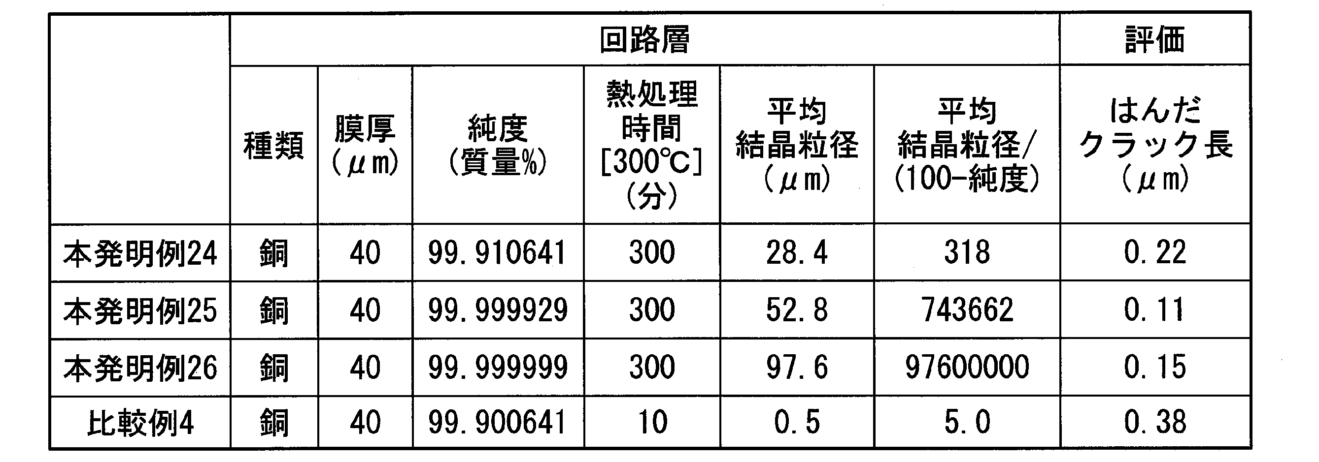
回路層に銅箔を用いた場合についても同様に、回路層の平均結晶粒径と純度とが、前記の式(1)を満足する本発明例24~26の金属ベース基板は、前記の式(1)を満足しない比較例4の金属ベース基板と比較して、冷熱サイクル付与後のはんだ層のクラック長さが短くなった。特に、回路層の平均結晶粒径と純度とが、前記の式(2)を満足し、平均結晶粒径が0.3μm以上で、純度が99.99質量%以上とされた本発明例25~26の金属ベース基板は、冷熱サイクル付与後のはんだ層のクラック長さが0.2μm以下と顕著に短くなった。
以上の結果から、本発明例によれば、はんだを介して電子部品を実装した状態で、冷熱サイクルを付与しても、はんだクラックの発生が起こりにくい金属ベース基板を提供することが可能となることが確認された。
はんだを介して電子部品を実装した状態で、冷熱サイクルを付与しても、はんだクラックの発生が起こりにくい金属ベース回路基板を提供することができる。
1 モジュール
2 金属ベース基板
3 電子部品
4 はんだ
10 金属基板
20 絶縁層
21 絶縁性樹脂
22 セラミック粒子
30 密着層
40 回路層
2 金属ベース基板
3 電子部品
4 はんだ
10 金属基板
20 絶縁層
21 絶縁性樹脂
22 セラミック粒子
30 密着層
40 回路層
Claims (5)
- 金属基板と、絶縁層と、回路層とがこの順で積層された金属ベース基板であって、
前記絶縁層は、樹脂を含み、
前記回路層は、膜厚が10μm以上1000μm以下の範囲内にあって、単位がμmで表される平均結晶粒径と単位が質量%で表される純度とが下記の式(1)を満足することを特徴とする金属ベース基板。
平均結晶粒径/(100-純度)>5 (1) - 前記回路層は、前記平均結晶粒径と前記純度とが下記の式(2)を満足することを特徴とする請求項1に記載の金属ベース基板。
平均結晶粒径/(100-純度)>20 (2) - 前記回路層は、前記平均結晶粒径が0.3μm以上であることを特徴とする請求項1又は2に記載の金属ベース基板。
- 前記回路層は、前記純度が99.99質量%以上であることを特徴とする請求項1から3のいずれか一項に記載の金属ベース基板。
- 前記回路層は、アルミニウムからなることを特徴とする請求項1から4のいずれか一項に記載の金属ベース基板。
Priority Applications (4)
| Application Number | Priority Date | Filing Date | Title |
|---|---|---|---|
| EP19837196.5A EP3826436A4 (en) | 2018-07-18 | 2019-07-17 | METAL BASE SUBSTRATE |
| CN201980047015.4A CN112425271A (zh) | 2018-07-18 | 2019-07-17 | 金属基底基板 |
| US17/258,565 US20210298170A1 (en) | 2018-07-18 | 2019-07-17 | Metal base substrate |
| KR1020217000426A KR20210031458A (ko) | 2018-07-18 | 2019-07-17 | 금속 베이스 기판 |
Applications Claiming Priority (2)
| Application Number | Priority Date | Filing Date | Title |
|---|---|---|---|
| JP2018134789A JP7147313B2 (ja) | 2018-07-18 | 2018-07-18 | 金属ベース基板 |
| JP2018-134789 | 2018-07-18 |
Publications (1)
| Publication Number | Publication Date |
|---|---|
| WO2020017550A1 true WO2020017550A1 (ja) | 2020-01-23 |
Family
ID=69165149
Family Applications (1)
| Application Number | Title | Priority Date | Filing Date |
|---|---|---|---|
| PCT/JP2019/028080 WO2020017550A1 (ja) | 2018-07-18 | 2019-07-17 | 金属ベース基板 |
Country Status (7)
| Country | Link |
|---|---|
| US (1) | US20210298170A1 (ja) |
| EP (1) | EP3826436A4 (ja) |
| JP (1) | JP7147313B2 (ja) |
| KR (1) | KR20210031458A (ja) |
| CN (1) | CN112425271A (ja) |
| TW (1) | TW202019247A (ja) |
| WO (1) | WO2020017550A1 (ja) |
Families Citing this family (3)
| Publication number | Priority date | Publication date | Assignee | Title |
|---|---|---|---|---|
| JP2021163827A (ja) * | 2020-03-31 | 2021-10-11 | 三菱マテリアル株式会社 | 金属ベース基板、電子部品実装基板 |
| JP2021163880A (ja) * | 2020-03-31 | 2021-10-11 | 三菱マテリアル株式会社 | 銅ベース基板 |
| JP2023055139A (ja) * | 2021-10-05 | 2023-04-17 | 三菱マテリアル株式会社 | 金属ベース基板 |
Citations (7)
| Publication number | Priority date | Publication date | Assignee | Title |
|---|---|---|---|---|
| JP2000256081A (ja) * | 1999-03-08 | 2000-09-19 | Mitsubishi Materials Corp | 半導体実装用絶縁基板の改質方法 |
| JP2006128286A (ja) * | 2004-10-27 | 2006-05-18 | Kyocera Corp | 金属セラミック複合体とその接合方法およびこれを用いた放熱基板 |
| JP2007201359A (ja) * | 2006-01-30 | 2007-08-09 | Nitto Denko Corp | 配線回路基板 |
| JP2011146679A (ja) * | 2009-12-18 | 2011-07-28 | Dainippon Printing Co Ltd | サスペンション回路基板、ハードディスク用サスペンションおよびハードディスクドライブ |
| JP5665449B2 (ja) | 2010-09-17 | 2015-02-04 | 新日鉄住金化学株式会社 | 金属張積層体及び熱伝導性ポリイミドフィルム |
| JP2017152610A (ja) | 2016-02-26 | 2017-08-31 | デンカ株式会社 | 回路基板及び電子部品搭載基板 |
| JP2018134789A (ja) | 2017-02-22 | 2018-08-30 | 三菱ケミカル株式会社 | 繊維強化樹脂材料および繊維強化樹脂成形体 |
Family Cites Families (19)
| Publication number | Priority date | Publication date | Assignee | Title |
|---|---|---|---|---|
| JP2000022289A (ja) * | 1998-07-01 | 2000-01-21 | Denki Kagaku Kogyo Kk | 回路基板用樹脂組成物とそれを用いた回路基板 |
| EP1055650B1 (en) * | 1998-11-11 | 2014-10-29 | Totankako Co., Ltd. | Carbon-based metal composite material, method for preparation thereof and use thereof |
| KR100657729B1 (ko) * | 1999-10-21 | 2006-12-13 | 신닛테츠가가쿠 가부시키가이샤 | 적층체 및 그의 제조방법 |
| JP4349952B2 (ja) * | 2004-03-24 | 2009-10-21 | 京セラ株式会社 | ウェハ支持部材とその製造方法 |
| JP5105217B2 (ja) * | 2005-04-25 | 2012-12-26 | 大日本印刷株式会社 | 金属積層体 |
| TWI449137B (zh) * | 2006-03-23 | 2014-08-11 | Ceramtec Ag | 構件或電路用的攜帶體 |
| JP5028147B2 (ja) * | 2007-05-29 | 2012-09-19 | 株式会社アライドマテリアル | 半導体装置用ヒートスプレッダとその製造方法 |
| US7957100B1 (en) * | 2007-08-29 | 2011-06-07 | Magnecomp Corporation | Disk drive gimbal having reduced residual stress and related method of manufacture |
| JP5359644B2 (ja) * | 2009-07-23 | 2013-12-04 | 三菱マテリアル株式会社 | パワーモジュール用基板、パワーモジュール及びパワーモジュール用基板の製造方法 |
| JP2011084800A (ja) * | 2009-10-19 | 2011-04-28 | Sumitomo Chemical Co Ltd | 高純度アルミニウム圧延板とその圧延板の製造方法 |
| WO2011058607A1 (ja) * | 2009-11-13 | 2011-05-19 | 株式会社日立製作所 | 絶縁性構造及びその製造方法 |
| JP6010926B2 (ja) * | 2012-02-29 | 2016-10-19 | 三菱マテリアル株式会社 | 接合材料、パワーモジュール及びパワーモジュールの製造方法 |
| JP6127540B2 (ja) * | 2012-03-30 | 2017-05-17 | 三菱マテリアル株式会社 | パワーモジュール用基板の製造方法 |
| JP6027823B2 (ja) * | 2012-09-07 | 2016-11-16 | 三菱マテリアル株式会社 | 熱延銅板、及び、熱延銅板の形状調整方法 |
| JP6621076B2 (ja) * | 2013-03-29 | 2019-12-18 | 三菱マテリアル株式会社 | パワーモジュール用基板、ヒートシンク付パワーモジュール用基板及びパワーモジュール |
| CN106165090B (zh) * | 2014-04-25 | 2020-07-03 | 三菱综合材料株式会社 | 功率模块用基板单元及功率模块 |
| KR102453166B1 (ko) * | 2014-06-30 | 2022-10-07 | 미쓰비시 마테리알 가부시키가이샤 | 세라믹스/알루미늄 접합체의 제조 방법, 파워 모듈용 기판의 제조 방법, 및 세라믹스/알루미늄 접합체, 파워 모듈용 기판 |
| JP6189822B2 (ja) * | 2014-11-28 | 2017-08-30 | デンカ株式会社 | 窒化ホウ素樹脂複合体回路基板 |
| JP6462958B2 (ja) * | 2016-06-16 | 2019-01-30 | 三菱電機株式会社 | 半導体実装用放熱ベース板およびその製造方法 |
-
2018
- 2018-07-18 JP JP2018134789A patent/JP7147313B2/ja active Active
-
2019
- 2019-07-17 US US17/258,565 patent/US20210298170A1/en not_active Abandoned
- 2019-07-17 CN CN201980047015.4A patent/CN112425271A/zh active Pending
- 2019-07-17 WO PCT/JP2019/028080 patent/WO2020017550A1/ja active Application Filing
- 2019-07-17 EP EP19837196.5A patent/EP3826436A4/en active Pending
- 2019-07-17 KR KR1020217000426A patent/KR20210031458A/ko not_active Application Discontinuation
- 2019-07-18 TW TW108125387A patent/TW202019247A/zh unknown
Patent Citations (7)
| Publication number | Priority date | Publication date | Assignee | Title |
|---|---|---|---|---|
| JP2000256081A (ja) * | 1999-03-08 | 2000-09-19 | Mitsubishi Materials Corp | 半導体実装用絶縁基板の改質方法 |
| JP2006128286A (ja) * | 2004-10-27 | 2006-05-18 | Kyocera Corp | 金属セラミック複合体とその接合方法およびこれを用いた放熱基板 |
| JP2007201359A (ja) * | 2006-01-30 | 2007-08-09 | Nitto Denko Corp | 配線回路基板 |
| JP2011146679A (ja) * | 2009-12-18 | 2011-07-28 | Dainippon Printing Co Ltd | サスペンション回路基板、ハードディスク用サスペンションおよびハードディスクドライブ |
| JP5665449B2 (ja) | 2010-09-17 | 2015-02-04 | 新日鉄住金化学株式会社 | 金属張積層体及び熱伝導性ポリイミドフィルム |
| JP2017152610A (ja) | 2016-02-26 | 2017-08-31 | デンカ株式会社 | 回路基板及び電子部品搭載基板 |
| JP2018134789A (ja) | 2017-02-22 | 2018-08-30 | 三菱ケミカル株式会社 | 繊維強化樹脂材料および繊維強化樹脂成形体 |
Non-Patent Citations (1)
| Title |
|---|
| See also references of EP3826436A4 |
Also Published As
| Publication number | Publication date |
|---|---|
| EP3826436A1 (en) | 2021-05-26 |
| KR20210031458A (ko) | 2021-03-19 |
| JP2020013874A (ja) | 2020-01-23 |
| US20210298170A1 (en) | 2021-09-23 |
| CN112425271A (zh) | 2021-02-26 |
| TW202019247A (zh) | 2020-05-16 |
| EP3826436A4 (en) | 2022-04-20 |
| JP7147313B2 (ja) | 2022-10-05 |
Similar Documents
| Publication | Publication Date | Title |
|---|---|---|
| WO2020017550A1 (ja) | 金属ベース基板 | |
| CN110168719A (zh) | 传热构件及包含其的散热结构体 | |
| JP5502429B2 (ja) | 回路基板 | |
| EP3749069A1 (en) | Metal base substrate | |
| WO2020017543A1 (ja) | 金属ベース基板 | |
| WO2021192479A1 (ja) | 絶縁膜、金属ベース基板及び金属ベース基板の製造方法 | |
| JP2020136577A (ja) | 放熱基板 | |
| JP2017197648A (ja) | 回路基板用樹脂組成物とそれを用いた金属ベース回路基板 | |
| US20230111128A1 (en) | Metal base substrate, electronic component mounting substrate | |
| JP7259206B2 (ja) | 金属ベース基板 | |
| US20230105989A1 (en) | Copper base substrate | |
| WO2022149558A1 (ja) | 金属ベース基板 | |
| WO2023058667A1 (ja) | 金属ベース基板 | |
| JP2019169619A (ja) | 金属ベース基板およびモジュール | |
| WO2021192480A1 (ja) | 絶縁膜、金属ベース基板及び金属ベース基板の製造方法 | |
| JP2011094147A (ja) | 低弾性接着剤並びにこの接着剤を用いた積層物、接着剤付き放熱板、接着剤付き金属箔 | |
| TW202217856A (zh) | 金屬基材基板 | |
| JP2013254879A (ja) | 回路基板及び電子部品搭載基板 |
Legal Events
| Date | Code | Title | Description |
|---|---|---|---|
| 121 | Ep: the epo has been informed by wipo that ep was designated in this application |
Ref document number: 19837196 Country of ref document: EP Kind code of ref document: A1 |
|
| NENP | Non-entry into the national phase |
Ref country code: DE |
|
| WWE | Wipo information: entry into national phase |
Ref document number: 2019837196 Country of ref document: EP |
|
| ENP | Entry into the national phase |
Ref document number: 2019837196 Country of ref document: EP Effective date: 20210218 |