WO2020017455A1 - 偏光板 - Google Patents
偏光板 Download PDFInfo
- Publication number
- WO2020017455A1 WO2020017455A1 PCT/JP2019/027718 JP2019027718W WO2020017455A1 WO 2020017455 A1 WO2020017455 A1 WO 2020017455A1 JP 2019027718 W JP2019027718 W JP 2019027718W WO 2020017455 A1 WO2020017455 A1 WO 2020017455A1
- Authority
- WO
- WIPO (PCT)
- Prior art keywords
- groove
- polarizing plate
- cross
- layer
- depth
- Prior art date
- Legal status (The legal status is an assumption and is not a legal conclusion. Google has not performed a legal analysis and makes no representation as to the accuracy of the status listed.)
- Ceased
Links
Images











Classifications
-
- G—PHYSICS
- G02—OPTICS
- G02B—OPTICAL ELEMENTS, SYSTEMS OR APPARATUS
- G02B5/00—Optical elements other than lenses
- G02B5/30—Polarising elements
- G02B5/3025—Polarisers, i.e. arrangements capable of producing a definite output polarisation state from an unpolarised input state
- G02B5/3058—Polarisers, i.e. arrangements capable of producing a definite output polarisation state from an unpolarised input state comprising electrically conductive elements, e.g. wire grids, conductive particles
-
- G—PHYSICS
- G02—OPTICS
- G02F—OPTICAL DEVICES OR ARRANGEMENTS FOR THE CONTROL OF LIGHT BY MODIFICATION OF THE OPTICAL PROPERTIES OF THE MEDIA OF THE ELEMENTS INVOLVED THEREIN; NON-LINEAR OPTICS; FREQUENCY-CHANGING OF LIGHT; OPTICAL LOGIC ELEMENTS; OPTICAL ANALOGUE/DIGITAL CONVERTERS
- G02F1/00—Devices or arrangements for the control of the intensity, colour, phase, polarisation or direction of light arriving from an independent light source, e.g. switching, gating or modulating; Non-linear optics
- G02F1/01—Devices or arrangements for the control of the intensity, colour, phase, polarisation or direction of light arriving from an independent light source, e.g. switching, gating or modulating; Non-linear optics for the control of the intensity, phase, polarisation or colour
- G02F1/13—Devices or arrangements for the control of the intensity, colour, phase, polarisation or direction of light arriving from an independent light source, e.g. switching, gating or modulating; Non-linear optics for the control of the intensity, phase, polarisation or colour based on liquid crystals, e.g. single liquid crystal display cells
- G02F1/133—Constructional arrangements; Operation of liquid crystal cells; Circuit arrangements
- G02F1/1333—Constructional arrangements; Manufacturing methods
- G02F1/1335—Structural association of cells with optical devices, e.g. polarisers or reflectors
-
- G—PHYSICS
- G03—PHOTOGRAPHY; CINEMATOGRAPHY; ANALOGOUS TECHNIQUES USING WAVES OTHER THAN OPTICAL WAVES; ELECTROGRAPHY; HOLOGRAPHY
- G03B—APPARATUS OR ARRANGEMENTS FOR TAKING PHOTOGRAPHS OR FOR PROJECTING OR VIEWING THEM; APPARATUS OR ARRANGEMENTS EMPLOYING ANALOGOUS TECHNIQUES USING WAVES OTHER THAN OPTICAL WAVES; ACCESSORIES THEREFOR
- G03B21/00—Projectors or projection-type viewers; Accessories therefor
- G03B21/005—Projectors using an electronic spatial light modulator but not peculiar thereto
- G03B21/006—Projectors using an electronic spatial light modulator but not peculiar thereto using LCD's
-
- G—PHYSICS
- G03—PHOTOGRAPHY; CINEMATOGRAPHY; ANALOGOUS TECHNIQUES USING WAVES OTHER THAN OPTICAL WAVES; ELECTROGRAPHY; HOLOGRAPHY
- G03B—APPARATUS OR ARRANGEMENTS FOR TAKING PHOTOGRAPHS OR FOR PROJECTING OR VIEWING THEM; APPARATUS OR ARRANGEMENTS EMPLOYING ANALOGOUS TECHNIQUES USING WAVES OTHER THAN OPTICAL WAVES; ACCESSORIES THEREFOR
- G03B21/00—Projectors or projection-type viewers; Accessories therefor
- G03B21/14—Details
-
- G—PHYSICS
- G03—PHOTOGRAPHY; CINEMATOGRAPHY; ANALOGOUS TECHNIQUES USING WAVES OTHER THAN OPTICAL WAVES; ELECTROGRAPHY; HOLOGRAPHY
- G03B—APPARATUS OR ARRANGEMENTS FOR TAKING PHOTOGRAPHS OR FOR PROJECTING OR VIEWING THEM; APPARATUS OR ARRANGEMENTS EMPLOYING ANALOGOUS TECHNIQUES USING WAVES OTHER THAN OPTICAL WAVES; ACCESSORIES THEREFOR
- G03B21/00—Projectors or projection-type viewers; Accessories therefor
- G03B21/14—Details
- G03B21/20—Lamp housings
- G03B21/2073—Polarisers in the lamp house
Definitions
- the wire grid type polarizing plate Since the wire grid type polarizing plate has high durability, it is suitably used, for example, in a liquid crystal projector having a high light density. In such a polarizing plate, an important requirement on optical characteristics is low reflection. When the reflectance is high, image quality is degraded due to a malfunction of the liquid crystal panel or stray light.
- the wire grid type polarizing plate includes, for example, a reflective layer, a dielectric layer, and an absorption layer.
- the S-polarized light parallel to the wire grid has an absorption effect of the upper dielectric layer and the absorption layer, and a three-layered structure. Suppression is performed using an interference effect (for example, see Patent Document 1).
- a groove that exposes the material of the substrate or the material of the underlying layer on the substrate may be formed between the grids, but depending on the shape of the groove, excellent optical characteristics may be obtained. could not be obtained.
- the present technology has been proposed in view of such circumstances, and provides a polarizing plate having excellent optical characteristics.
- the polarizing plate according to the present technology, a transparent substrate that is transparent to light in the wavelength band used, arranged on the transparent substrate at a pitch shorter than the wavelength of the light in the wavelength band used, extending in a predetermined direction And, a lattice-shaped convex portion having a reflective layer and a reflection control layer, and recessed between the lattice-shaped convex portions, the width in the direction orthogonal to the predetermined direction is reduced so as to become zero toward the depth direction. And a groove portion.
- an optical apparatus is characterized in that the above-described polarizing plate is mounted.
- the method for manufacturing a polarizing plate according to the present technology etching the reflection layer and the reflection control layer laminated on a transparent substrate that is transparent to light in the use wavelength band, from the wavelength of the light in the use band. Also arranged at a short pitch, a lattice-shaped protrusion extending in a predetermined direction, and recessed between the lattice-shaped protrusions, so that a width in a direction orthogonal to the predetermined direction becomes zero toward a depth direction. And a groove portion that becomes smaller.
- the transmittance characteristics and the reflectance characteristics can be improved, and excellent optical characteristics can be obtained.
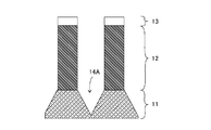
- FIG. 1 is a cross-sectional view schematically showing the structure of a polarizing plate when the cross-sectional shape of the groove is substantially V-shaped.
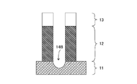
- FIG. 2 is a cross-sectional view schematically showing the structure of the polarizing plate when the cross-sectional shape of the groove is substantially U-shaped.
- FIG. 3 is a cross-sectional view schematically showing the structure of the polarizing plate when the cross-sectional shape of the groove is asymmetric.
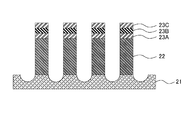
- FIG. 4 is a cross-sectional view schematically showing the structure of the polarizing plate shown as specific example 1.
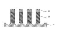
- FIG. 5 is a cross-sectional view schematically showing the structure of a polarizing plate shown as specific example 2.
- FIG. 1 is a cross-sectional view schematically showing the structure of a polarizing plate when the cross-sectional shape of the groove is substantially V-shaped.
- FIG. 2 is a cross-sectional view schematically showing the structure of the polarizing plate when the cross-sectional shape of the groove is substantially
- FIG. 6 is a cross-sectional view schematically showing a structure of a polarizing plate shown as a modification.
- FIG. 7 is a cross-sectional view schematically illustrating a configuration of a polarizing plate in a case where a cross-sectional shape of a groove portion according to a conventional example is a quadrangular shape.
- FIG. 8 is a graph showing a simulation result of a transmission axis transmittance Tp of a polarizing plate when a groove having a rectangular cross section, which is a conventional example, has a predetermined depth.
- FIG. 8 is a graph showing a simulation result of a transmission axis transmittance Tp of a polarizing plate when a groove having a rectangular cross section, which is a conventional example, has a predetermined depth.
- FIG. 9 is a graph showing a simulation result of a transmission axis reflectance Rp of a polarizing plate when a groove having a rectangular cross section, which is a conventional example, has a predetermined depth.
- FIG. 10 is a cross-sectional view schematically illustrating a configuration of a polarizing plate when the cross-sectional shape of the groove is substantially V-shaped.
- FIG. 11 is a graph showing a simulation result of the transmission axis transmittance Tp of the polarizing plate when the groove having a substantially V-shaped cross section is set to a predetermined depth.
- FIG. 12 is a graph showing a simulation result of the transmission axis reflectance Rp of the polarizing plate when the groove having a substantially V-shaped cross section is set to a predetermined depth.
- FIG. 13 is a graph showing a simulation result of the average value of the transmission axis transmittance Tp of each wavelength band of the polarizing plate when a groove having a rectangular cross section as a conventional example is set to a predetermined depth.
- FIG. 14 is a graph showing a simulation result of the average value of the transmission axis transmittance Tp of each wavelength band of the polarizing plate when the groove having a substantially V-shaped cross section is set to a predetermined depth.
- FIG. 15 is a cross-sectional view schematically illustrating a configuration of a polarizing plate when the cross-sectional shape of the groove is substantially U-shaped.
- FIG. 16 is a cross-sectional view schematically illustrating a configuration of the groove when the cross-sectional shape of the groove is substantially U-shaped.
- FIG. 17 is a graph showing a curve of the cross-sectional shape of the groove when the cross-sectional shape of the groove is substantially U-shaped.
- FIG. 18 is a graph showing a simulation result of the transmission axis transmittance Tp of the polarizing plate when a groove having a substantially U-shaped cross section is set to a predetermined depth.
- FIG. 19 is a graph showing a simulation result of the transmission axis reflectance Rp of the polarizing plate when the groove having a substantially U-shaped cross section is set to a predetermined depth.
- FIG. 20 is a graph showing a simulation result of the average value of the transmission axis transmittance Tp in the green wavelength band with respect to the depth of the groove having a substantially U-shaped cross section.
- FIG. 21 is a graph showing a simulation result of the average value of the transmission axis reflectance Rp in the green wavelength band with respect to the depth of the groove having a substantially U-shaped cross section.
- FIG. 22 is a graph showing a relationship between an angle between a perpendicular passing through the midpoint (origin) of the width when the depth of the groove is zero and a straight line passing through the deepest part of the groove and the origin.
- FIG. 23 is a graph showing a simulation result of the transmission axis transmittance Tp of the polarizing plate when the cross-sectional shape of the groove is set to a curve (a), a curve (b), and a curve (c).
- FIG. 24 is a graph showing a simulation result of the transmission axis reflectance Rp of the polarizing plate when the cross-sectional shape of the groove is set to the curve (a), the curve (b), and the curve (c).
- FIG. 25 is a graph showing a green wavelength band for a polarizing plate in which the angle between a perpendicular line passing through the midpoint (origin) of the width when the depth of the groove is zero and a straight line passing through the deepest part of the groove and the origin is ⁇ .
- 7 is a graph showing a simulation result of the average value of the transmission axis transmittance Tp of FIG.
- FIG. 26 shows the green wavelength band of the polarizing plate when the angle between the perpendicular passing through the midpoint (origin) of the width when the depth of the groove is zero and the straight line passing through the deepest part of the groove and the origin is ⁇ .
- 12 is a graph showing a simulation result of an average value of the transmission axis reflectance Rp of FIG.
- FIG. 27 is a simulation result of the average value of the transmission axis transmittance Tp in the green wavelength band for the polarizing plate when the cross-sectional shape is rectangular, substantially V-shaped, or substantially U-shaped and the groove has a predetermined depth.
- FIG. FIG. 28 is a graph showing a simulation result of a refractive index in a depth direction of a groove having a rectangular, substantially V-shaped, or substantially U-shaped cross section.
- Polarizing plate The polarizing plate according to the present embodiment, a transparent substrate that is transparent to light in the wavelength band used, arranged on the transparent substrate at a pitch shorter than the wavelength of light in the wavelength band used, extending in a predetermined direction, A lattice-shaped convex portion having a reflective layer and a reflection control layer, and a groove portion recessed between the lattice-shaped convex portions, the width of which in the direction perpendicular to the predetermined direction decreases so as to become zero toward the depth direction.
- the groove may be recessed in the transparent substrate, or may be recessed in a base layer formed on the transparent substrate.
- the underlayer is preferably made of a dielectric material having a refractive index equal to or lower than the refractive index of the transparent substrate, and is preferably made of Si oxide such as SiO 2 .
- FIG. 1 is a cross-sectional view schematically showing the structure of a polarizing plate when the cross-sectional shape of the groove is substantially V-shaped
- FIG. 2 is a cross-sectional view of the polarizing plate when the cross-sectional shape of the groove is substantially U-shaped
- FIG. 3 is a cross-sectional view schematically illustrating the structure of the polarizing plate when the cross-sectional shape of the groove is asymmetric.
- the polarizing plate includes a transparent substrate 11, a lattice-shaped protrusion having a reflective layer 12 and a reflection control layer 13, and grooves 14A and 14B recessed between the lattice-shaped protrusions. , 14C.
- the lattice-shaped protrusion has at least the reflection layer 12 and the reflection control layer 13.
- the pitch of the lattice-shaped convex portions is preferably smaller than the wavelength of light in the used band, and specifically, is preferably 100 nm or more and 200 nm or less. Further, it is preferable that the ratio of the length in the direction (Y direction) parallel to the longitudinal direction of the wire grid with respect to the height of the lattice-shaped protrusion is 1,000 or more. Further, the ratio of the length in the Y direction to the depth of the grooves 14A, 14B, 14C is preferably 1000 or more. Further, it is preferable that the lattice-shaped protrusions and the grooves 14A, 14B, 14C are parallel to the Y direction. Thereby, even when used in a liquid crystal element formed of micron-sized pixels, the in-plane transmittance and reflectance can be made uniform.
- the reflection layer 12 is formed by extending a light-reflective material having a reflectivity for light in the used wavelength band in the Y direction, which is the absorption axis, in a band shape. That is, the reflective layer 12 has a function as a wire grid polarizer, and among the light incident on the surface of the transparent substrate on which the wire grid is formed, the direction parallel to the longitudinal direction of the wire grid (Y direction). ) Attenuates a polarized wave (TE wave (S wave)) having an electric field component and transmits a polarized wave (TM wave (P wave)) having an electric field component in a direction (X direction) orthogonal to the longitudinal direction of the wire grid. Let it.
- TE wave S wave
- TM wave polarized wave
- the reflection control layer 13 attenuates the TE wave by selective light absorption of the polarized wave.
- a part of the TE wave reflected by the reflection layer 12 can be reflected when passing through the reflection control layer 13 and returned to the reflection layer 12.
- Light passing through the control layer 13 can be attenuated by interference.
- the configuration of the reflection control layer 13 includes, for example, a multilayer film including an absorption layer made of a light-absorbing material having absorptivity to light in a used wavelength band and a dielectric layer made of a dielectric.
- it may be a reflection suppressing layer formed by mixing a light absorbing material and a dielectric.
- the grooves 14A, 14B, and 14C are reduced so that the width in the direction orthogonal to the predetermined direction becomes zero toward the depth direction.
- the air portion becomes larger with respect to the substrate material from the deepest portion toward the substrate surface.
- the cross-sectional shape of the groove in a direction orthogonal to the predetermined direction that is, the cross-sectional shape of the groove when viewed from the predetermined direction does not have a bottom surface.
- having no bottom means that the width of the bottom in a direction orthogonal to the predetermined direction is 10 nm or less.
- the cross section of the groove in a direction orthogonal to the predetermined direction can be substantially V-shaped.
- the transmission axis transmittance Tp is increased and the transmission axis reflectance Rp is decreased, so that excellent optical characteristics can be obtained. it can.
- a decrease in the transmission axis transmittance Tp in the blue wavelength band (wavelength 430 to 510 nm) is suppressed as compared with the case where the cross-sectional shape of the groove is square. be able to.
- the depth of the groove is preferably 20 nm or more and 100 nm or less, more preferably 60 nm or more and 100 nm or less.
- the cross-sectional shape of the groove in a direction orthogonal to the predetermined direction can be substantially U-shaped.
- the green wavelength band (wavelength 520 to 590 nm) and the red wavelength band (wavelength 600 to 680 nm) are used.
- the transmission axis transmittance Tp is increased and the transmission axis reflectance Rp is decreased, so that excellent optical characteristics can be obtained.
- the cross-sectional shape of the groove is substantially U-shaped, a decrease in the transmission axis transmittance Tp in the blue wavelength band (wavelength 430 to 510 nm) is suppressed as compared with the case where the cross-sectional shape of the groove is square. I can do it.
- the depth of the groove is preferably 20 nm or more and 120 nm or less, more preferably 60 nm or more and 100 nm or less.
- the cross-sectional shape of the groove in a direction orthogonal to the predetermined direction may be asymmetric with respect to a perpendicular passing through the midpoint of the width when the depth of the groove is zero. it can. That is, the shape of the cross section of the groove does not have to be on a vertical line passing through the midpoint of the width when the deepest part of the groove is zero in depth. More specifically, it is preferable that the angle between the perpendicular passing through the midpoint (origin) of the width when the depth of the groove is zero and the straight line passing through the deepest part of the groove and the origin be ⁇ 20 ° or less. .
- a polarizing plate having an angle of 0 ° between the deepest portion of the groove and a straight line passing through the origin, that is, the midpoint of the width when the cross-sectional shape of the groove in the direction orthogonal to the predetermined direction is zero is the depth of the groove.
- the cross-sectional shape of the groove is asymmetric, at least one of the inclinations is smaller than that of the other, so that it is possible to easily form a protective film such as a dielectric portion and a water-repellent portion.
- the protective film is formed on the surface of the lattice-shaped protrusions and the surface of the groove between the lattice-shaped protrusions by forming a dielectric portion, a water-repellent portion, and the like, and imparts a moisture resistance effect, a water-repellent effect, and the like. Can be improved.
- dielectric constituting the dielectric portion examples include Si oxides such as SiO 2 , metal oxides such as Al 2 O 3 , beryllium oxide and bismuth oxide, MgF 2 , cryolite, germanium, titanium dioxide, silicon, Common materials such as magnesium fluoride, boron nitride, boron oxide, tantalum oxide, carbon, or a combination thereof can be used. Among these, Si oxides such as SiO 2 are preferably used.
- the water-repellent portion is formed using a water-repellent compound, and suppresses entry of moisture between grids due to capillary action.
- the water-repellent compound include a silane compound having a fluoroalkyl group or an alkyl group, and a phosphoric acid compound.
- the alkyl chain preferably has 4 to 20 carbon atoms.
- silane compound examples include, for example, FDTS (heptadecafluoro-1,1,2,2-tetrahydrodecyltrichlorosilane), PETS (pentafuorophenylpropyltrichlorosilane), FOTS ((tridecafluoro-1,1,2,2-tetrahydrooctyl) trichlorosilane), and OTS ( n-octadecyltrichlorosilane, (C18)) and the like.
- FDTS heptadecafluoro-1,1,2,2-tetrahydrodecyltrichlorosilane
- PETS penentafuorophenylpropyltrichlorosilane
- FOTS (tridecafluoro-1,1,2,2-tetrahydrooctyl) trichlorosilane)
- OTS n-octadecyltrichlorosilane, (C
- the phosphoric acid compound examples include FOPA (1H, 1H, 2H, 2H-perfluoro-n-octylphosphonic acid), FDPA (1H, 1H, 2H, 2H-perfluoro-n-decylphosphonic acid), FHPA (1H , 1H, 2H, 2H-perfluoro-n-hexylphosphonic acid, ODPA (octadecylphosphonic acid) and the like.
- FOPA 1H, 1H, 2H, 2H-perfluoro-n-octylphosphonic acid
- FDPA 1H, 1H, 2H, 2H-perfluoro-n-decylphosphonic acid
- FHPA 1H , 1H, 2H, 2H-perfluoro-n-hexylphosphonic acid
- ODPA octadecylphosphonic acid
- a polarized wave (TE wave) having an electric field component parallel to the grating of the reflective layer is utilized by utilizing the four effects of transmission, reflection, interference, and selective light absorption of a polarized wave. (S wave)), and a polarized wave (TM wave (P wave)) having an electric field component perpendicular to the grating can be transmitted. That is, the TE wave is attenuated by the selective light absorption of the polarized wave of the reflection suppressing layer, and the TE wave transmitted through the reflection control layer is reflected by the grid-like reflective layer functioning as a wire grid.
- the transmittance characteristics and the reflectance characteristics can be improved, and excellent optical characteristics can be obtained.
- the groove structure is optimized only by changing the manufacturing process of the polarizing plate without significantly changing the structure of the polarizing plate, and optical characteristics are improved. What you can do is extremely useful industrially.
- FIG. 4 is a cross-sectional view schematically showing the structure of the polarizing plate shown as specific example 1.
- the polarizers are arranged on a transparent substrate 21 that is transparent to the light in the operating wavelength band, and on the transparent substrate at a pitch shorter than the wavelength of the light in the operating band, and extend in a predetermined direction.
- a reflective layer 22 a first dielectric layer 23A, an absorbing layer 23B, and a second dielectric layer 23C in this order.
- a groove portion whose width in a direction orthogonal to the width direction becomes smaller toward zero in the depth direction. That is, the polarizing plate shown as the specific example 1 has a first dielectric layer 23A, an absorption layer 23B, and a second dielectric layer 23C as reflection control layers.
- the transparent substrate 21 is not particularly limited as long as it is a substrate that transmits light in the band of use, and can be appropriately selected according to the purpose.
- the expression "transmissive to light in the used band” does not mean that the transmittance of light in the used band is 100%, but a light transmissivity capable of maintaining the function as a polarizing plate. Just show it.
- Examples of the light in the use band include visible light having a wavelength of about 380 nm to 810 nm.
- the material of the reflection layer 22 is not particularly limited as long as it is a material having reflectivity to light in a use band.
- a material having reflectivity to light in a use band For example, Al, Ag, Cu, Mo, Cr, Ti, Ni, W, Fe, Si, Ge, Te Metal, an alloy containing these, or a semiconductor material.
- the first dielectric layer 23A is formed, for example, to have a thickness such that the polarized light reflected by the absorbing layer 23B is transmitted through the absorbing layer 23B and the phase of the polarized light reflected by the reflecting layer 22 is shifted by a half wavelength.
- the film thickness is not optimized, the light reflected by the absorption layer 23B can be absorbed and the contrast can be improved, so that it may be determined in consideration of the desired polarization characteristics and the actual manufacturing process. .
- Si oxide such as SiO 2 , metal oxide such as Al 2 O 3 , beryllium oxide, bismuth oxide, MgF 2 , cryolite, germanium, titanium dioxide, silicon, fluorine Common materials such as magnesium oxide, boron nitride, boron oxide, tantalum oxide, carbon, or a combination thereof can be used. Among these, Si oxide is preferably used.
- the absorption layer 23B is made of a light-absorbing material having a light absorption function, such as a metal material or a semiconductor material, having a non-zero optical constant extinction constant, and is appropriately selected depending on light in a use band.
- a metal material include elemental elements such as Ta, Al, Ag, Cu, Au, Mo, Cr, Ti, W, Ni, Fe, and Sn, and alloys containing one or more of these elements.
- the semiconductor material include Si, Ge, Te, ZnO, and silicide materials ( ⁇ -FeSi 2 , MgSi 2 , NiSi 2 , BaSi 2 , CrSi 2 , CoSi 2 , TaSi, and the like).
- the polarizing plate can obtain a high extinction ratio with respect to a visible light range to which the polarizing plate is applied.
- the same material as the first dielectric layer 23A can be used for the second dielectric layer 23C, and among them, Si oxide such as SiO 2 is preferably used.
- FIG. 5 is a cross-sectional view schematically showing the structure of a polarizing plate shown as specific example 2.
- the polarizers are arranged on a transparent substrate 31 that is transparent to light in the operating wavelength band, and on the transparent substrate at a pitch shorter than the wavelength of light in the operating band, and extend in a predetermined direction.
- the transparent substrate 31 and the reflective layer 32 are the same as the transparent substrate 21 and the reflective layer 22 of the polarizing plate shown in the specific example 1 described above, respectively, and the description is omitted here.
- the reflection suppressing layer 33 is formed by mixing a light absorbing material and a dielectric, and has, for example, a concentration distribution in which the concentration of the light absorbing material or the dielectric is inclined in the layer thickness direction.
- the light-absorbing material examples include a metal material and a semiconductor material, which are appropriately selected according to the light in the working band.
- the metal material include elemental elements such as Ta, Al, Ag, Cu, Au, Mo, Cr, Ti, W, Ni, Fe, and Sn, and alloys containing one or more of these elements.
- the semiconductor material include Si, Ge, Te, ZnO, and silicide materials ( ⁇ -FeSi 2 , MgSi 2 , NiSi 2 , BaSi 2 , CrSi 2 , CoSi 2 , TaSi, and the like).
- a carbon material such as a carbon nanotube or graphene may be used as the light absorbing material.
- dielectric examples include Si oxide such as SiO 2 , metal oxides such as Al 2 O 3 , beryllium oxide and bismuth oxide, MgF 2 , cryolite, germanium, titanium dioxide, silicon, magnesium fluoride, and boron nitride. , Boron oxide, tantalum oxide, carbon, or a combination thereof. Among these, Si oxide is preferably used.
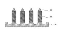
- FIG. 6 is a cross-sectional view schematically showing a structure of a polarizing plate shown as a modification.
- the polarizing plates are arranged on a transparent substrate 41 that is transparent to light in a used wavelength band, and on a transparent substrate at a pitch shorter than the wavelength of light in a used band, and extend in a predetermined direction.
- a reflection layer 42, a light absorbing material and a dielectric material, and a reflection suppressing layer 43 having a width in a direction perpendicular to the predetermined direction that becomes smaller toward the distal end;
- the transparent substrate 41 and the reflective layer 42 are the same as the transparent substrate 31 and the reflective layer 32 of the polarizing plate shown in the specific example 2 described above, respectively, the description is omitted here.
- the reflection suppressing layer 43 is formed by mixing a light absorbing material and a dielectric, and has, for example, a concentration distribution in which the concentration of the light absorbing material or the dielectric is inclined in the layer thickness direction.
- the light-absorbing material and the dielectric the same materials as those in the specific example 2 can be used.
- the reflection suppressing layer 43 has a grid tip portion whose width in the direction orthogonal to the predetermined direction becomes smaller toward the tip.
- the grid tip has a tapered shape having, for example, the shape of an equilateral trapezoid.
- the above-described modification has been described as a modification of the polarizing plate shown in the specific example 2, it may be a modification of the polarizing plate shown in the specific example 1.
- the leading end of the grid is composed of a first dielectric layer 23A, an absorption layer 23B, and a second dielectric layer 23C.
- the manufacturing method of the polarizing plate according to the present embodiment etching the reflective layer and the reflection control layer laminated on a transparent substrate that is transparent to light in the use wavelength band, shorter than the wavelength of light in the use band.
- Lattice-shaped protrusions that are arranged at a pitch and extend in a predetermined direction, and grooves that are recessed between the lattice-shaped protrusions and have a width that decreases in a direction perpendicular to the predetermined direction so as to become zero toward the depth direction. And are formed.
- a reflection layer and a reflection control layer are laminated on a transparent substrate by, for example, a sputtering method.
- a photosensitive resin is applied as a resist, and exposure and development are performed to form a lattice pattern of the resist.
- the grid pattern of the resist is transferred to the lower reflective layer and the reflection control layer to form a lattice-like convex portion having the reflective layer and the reflection control layer, and a groove is formed between the lattice-like convex portions.
- the etching gas for example, when aluminum is used for the reflection layer, chlorine-based plasma is preferably used, and when SiO 2 or FeSi is used for the reflection control layer, fluorine-based plasma is preferably used.
- Al 2 O 3 is used, BCl 3 is preferably used.
- the width of the cross-sectional shape becomes smaller toward zero in the depth direction.
- a plasma etching apparatus for forming the groove.
- the etching gas is preferably a mixed gas of a CF-based gas (particularly CF 4 ) and Ar, and the gas pressure is preferably 0.5 to 1.0 Pa and the bias is preferably 40 to 200 W.
- a Cl-based gas (particularly, a mixed gas of Cl 2 and BCl 3 ) is used as the etching gas, and the gas pressure is 0.5 to 1.0 Pa and the bias is 30 to Preferably, it is set to 50W.
- the gas pressure is 0.5 to 1.0 Pa and the bias is 30 to Preferably, it is set to 50W.
- a groove is formed so that the width of the cross-sectional shape becomes smaller in the depth direction so as to become zero, and a polarizing plate having excellent optical characteristics can be obtained.
- a protective film such as a dielectric portion or a water-repellent portion may be formed on the surface of the lattice-shaped protrusions and the surface of the groove between the lattice-shaped protrusions.
- the dielectric portion can be formed by a physical vapor deposition method, a chemical vapor deposition method, or the like. Among these, it is particularly preferable to use the ALD method (Atomic Layer Deposition method, atomic deposition method). As a result, even in a trench structure having a high aspect ratio, the dielectric can be uniformly attached to the details of the groove.
- the water-repellent portion can be formed by applying a water-repellent compound to the surface of the lattice-shaped protrusions and the surface of the groove between the lattice-shaped protrusions.
- a water-repellent compound examples include dip coating, spin coating, and vapor treatment. Among these, it is particularly preferable to use a vapor treatment.
- the water-repellent compound can be applied to the details of the trench structure having a high aspect ratio.
- the optical device according to the present embodiment is equipped with the above-described polarizing plate.
- the optical device include a liquid crystal projector, a head-up display, a digital camera, and the like. Since the polarizing plate according to the present embodiment has a high transmittance, it is suitable for applications such as a liquid crystal projector and a head-up display that require high luminance.
- the optical device according to the present embodiment includes a plurality of polarizing plates
- at least one of the plurality of polarizing plates may be a polarizing plate according to the present technology.
- the optical device according to the present embodiment is a liquid crystal projector
- at least one of the polarizing plates disposed on the incident side and the emitting side of the liquid crystal panel may be a polarizing plate according to the present technology.
- Example> Hereinafter, embodiments of the present technology will be described.
- a simulation was performed on the shape of the groove recessed in the substrate between the lattice-shaped protrusions. Note that the present technology is not limited to these embodiments.
- the simulation was performed by an electromagnetic field simulation by the RCWA (Rigorous Coupled Wave Analysis) method.
- RCWA Ragorous Coupled Wave Analysis
- a grating simulator "Gsolver” manufactured by Grating @ Solver @ Development was used.
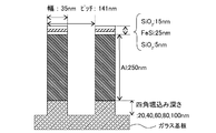
- FIG. 7 is a cross-sectional view schematically illustrating a configuration of a polarizing plate in a case where a cross-sectional shape of a groove portion according to a conventional example is a quadrangular shape.
- the polarizing plate shown in FIG. 7 includes a glass substrate, a reflective layer made of Al having a width W of 35 nm arranged at a pitch P of 141 nm on the glass substrate, a first SiO 2 layer disposed on the reflective layer, and FeSi. A second SiO 2 layer.
- the thickness T 42 of the reflective layer was 250 nm
- the thickness T 43 of the first SiO 2 layer was 5 nm
- the thickness T 44 of the first FeSi layer was 25 nm
- the thickness T 45 of the second SiO 2 layer was 15 nm.
- the Fe content in the FeSi layer was 5 atm%
- the Si content was 95 atm%.
- the simulation was performed by setting the cross-sectional shape of the groove formed in the glass substrate to be square, and setting the depth to 20 nm, 40 nm, 60 nm, 80 nm and 100 nm, respectively.
- Table 1 shows the simulation results of the average value of the transmission axis transmittance Tp and the transmission axis reflectance Rp of each wavelength band of the polarizing plate when the cross-sectional shape of the conventional groove is square.
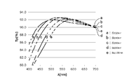
- FIG. 8 is a graph showing a simulation result of a transmission axis transmittance Tp of a polarizing plate when a groove having a rectangular cross-sectional shape as a conventional example is set to a predetermined depth
- FIG. 9 is a graph showing a conventional example
- 11 is a graph showing a simulation result of a transmission axis reflectance Rp of a polarizing plate when a groove having a certain cross-sectional shape is a rectangular shape and having a predetermined depth.
- the transmission axis reflectance Rp in the blue wavelength band (wavelength 430 to 510 nm) was significantly increased, and the optical characteristics were degraded.
- the transmission axis transmittance Tp in the green wavelength band (wavelength 520 to 590 nm) decreases, and the transmission axis transmittance Tp in the blue wavelength band (wavelength 430 to 510 nm) decreases.
- the depth of the groove is 60 nm or more, the transmission axis transmittance Tp in the green wavelength band (wavelength 520 to 590 nm) decreases, and the transmission axis transmittance Tp in the blue wavelength band (wavelength 430 to 510 nm) decreases.
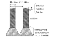
- FIG. 10 is a cross-sectional view schematically illustrating a configuration of a polarizing plate when the cross-sectional shape of the groove is substantially V-shaped.
- the polarizing plate shown in FIG. 10 had the same configuration as that of the polarizing plate shown in FIG. 7 except that the cross-sectional shape of the groove formed in the substrate was substantially V-shaped. That is, the polarizing plate includes a glass substrate, a reflective layer made of Al having a width of 35 nm and arranged on the glass substrate at a pitch P of 141 nm, a first SiO 2 layer disposed on the reflective layer, and an FeSi layer. And a second SiO 2 layer.
- the thickness T 52 of the reflective layer was 250 nm
- the thickness T 53 of the first SiO 2 layer was 5 nm
- the thickness T 54 of the first FeSi layer was 25 nm
- the thickness T 55 of the second SiO 2 layer was 15 nm.
- the Fe content in the FeSi layer was 5 atm%
- the Si content was 95 atm%.
- a simulation was performed by setting the cross-sectional shape of the groove formed in the glass substrate to be a substantially V-shaped triangle and setting the depth to 20 nm, 40 nm, 60 nm, 80 nm, and 100 nm, respectively.
- Table 2 shows a simulation result of the average value of the transmission axis transmittance Tp and the transmission axis reflectance Rp of each wavelength band of the polarizing plate when the cross-sectional shape of the groove is substantially V-shaped.
- FIG. 11 is a graph showing a simulation result of the transmission axis transmittance Tp of the polarizing plate when a groove having a substantially V-shaped cross section is set to a predetermined depth
- FIG. It is a graph which shows the simulation result of the transmission axis reflectance Rp of the polarizing plate at the time of making a character-shaped groove part into predetermined depth.
- FIG. 13 is a graph showing a simulation result of the average value of the transmission axis transmittance Tp in each wavelength band of the polarizing plate when a groove having a rectangular cross section, which is a conventional example, has a predetermined depth
- FIG. 14 is a graph showing a simulation result of the average value of the transmission axis transmittance Tp of each wavelength band of the polarizing plate when the groove having a substantially V-shaped cross section is set to a predetermined depth.
- the transmission axis transmittance Tp is increased and the transmission axis is increased in the green wavelength band (wavelength 520 to 590 nm) and the red wavelength band (wavelength 600 to 680 nm). It was found that the reflectance Rp was reduced, and excellent optical characteristics were obtained. Further, when the cross-sectional shape of the groove is substantially V-shaped, a decrease in the transmission axis transmittance Tp in the blue wavelength band (wavelength 430 to 510 nm) is suppressed as compared with the case where the cross-sectional shape of the groove is square. I understood that.
- the transmission axis transmittance Tp in the blue wavelength band is larger than when the depth of the groove is 0 nm, and excellent optical characteristics can be obtained.
- FIG. 15 is a cross-sectional view schematically illustrating a configuration of a polarizing plate when the cross-sectional shape of the groove is substantially U-shaped.
- the polarizing plate shown in FIG. 15 has the same configuration as that of the polarizing plate shown in FIG. 7, except that the cross-sectional shape of the groove formed in the substrate is substantially U-shaped. That is, the polarizing plate includes a glass substrate, a reflective layer made of Al having a width of 35 nm and arranged on the glass substrate at a pitch P of 141 nm, a first SiO 2 layer disposed on the reflective layer, and an FeSi layer. And a second SiO 2 layer.
- the thickness T 52 of the reflective layer was 250 nm
- the thickness T 53 of the first SiO 2 layer was 5 nm
- the thickness T 54 of the first FeSi layer was 25 nm
- the thickness T 55 of the second SiO 2 layer was 15 nm.
- the Fe content in the FeSi layer was 5 atm%
- the Si content was 95 atm%.
- the simulation was performed by setting the cross-sectional shape of the groove formed in the glass substrate to be substantially U-shaped, and setting the depth to 20 nm, 40 nm, 60 nm, 80 nm, 100 nm, and 120 nm, respectively.
- FIG. 16 is a cross-sectional view schematically illustrating a configuration of the groove when the cross-sectional shape of the groove is substantially U-shaped
- FIG. 17 is a cross-sectional view of the groove when the cross-sectional shape of the groove is substantially U-shaped. It is a graph which shows a curve of a shape.
- the cross-sectional shape of the groove portion was defined as the origin (0, 0) at the midpoint of the width when the depth of the groove portion was zero, the grid interval was W, and the groove depth was D.
- FIG. 18 is a graph showing a simulation result of a transmission axis transmittance Tp of the polarizing plate when a groove having a substantially U-shaped cross section is set to a predetermined depth
- FIG. 19 is a graph showing a substantially U-shaped cross section.
- 12 is a graph showing a simulation result of a transmission axis reflectance Rp of a polarizing plate when a groove portion having a predetermined depth is set.
- FIG. 20 is a graph showing a simulation result of an average value of a transmission axis transmittance Tp in a green wavelength band with respect to a depth of a groove having a substantially U-shaped cross section.
- FIG. It is a graph which shows the simulation result of the average value of the transmission axis reflectance Rp of a green wavelength band with respect to the depth of the groove part which made the character shape.
- the transmission axis transmittance Tp is increased in the green wavelength band (wavelength 520 to 590 nm) and the red wavelength band (wavelength 600 to 680 nm), and the transmission axis is increased. It was found that the reflectance Rp was reduced, and excellent optical characteristics were obtained. Further, when the cross-sectional shape of the groove is substantially U-shaped, a decrease in the transmission axis transmittance Tp in the blue wavelength band (wavelength 430 to 510 nm) is suppressed as compared with the case where the cross-sectional shape of the groove is square. I understood that.
- the transmission axis transmittance Tp in the green wavelength band is large and the transmission axis reflectance Rp in the green wavelength band is small, so that excellent optical characteristics can be obtained.
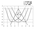
- FIG. 22 is a graph showing a relationship between an angle between a perpendicular passing through the midpoint (origin) of the width when the depth of the groove is zero and a straight line passing through the deepest part of the groove and the origin.
- the curve (b) is a perpendicular line passing through the midpoint (origin) of the width when the depth of the groove is zero
- a curve having an angle of 20 ° with a straight line connecting the deepest part of the curve (b) is shown
- a curve (c) shows a perpendicular line passing through the midpoint (origin) of the width when the depth of the groove is zero.
- the polarizing plate had the same configuration as the polarizing plate shown in FIG. 15 except that the cross-sectional shape of the groove formed in the substrate was curved (a), curved (b), and curved (c).
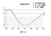
- FIG. 23 is a graph showing a simulation result of the transmission axis transmittance Tp of the polarizing plate when the cross-sectional shape of the groove is set to curve (a), curve (b), and curve (c), and FIG. It is a graph which shows the simulation result of the transmission axis reflectance Rp of a polarizing plate when a cross-sectional shape is made into curve (a), curve (b), and curve (c).
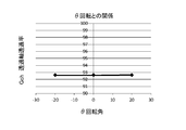
- FIG. 25 shows a polarizing plate in which the angle between a perpendicular line passing through the midpoint (origin) of the width when the depth of the groove is zero and a straight line passing through the deepest part of the groove and the origin is ⁇ .
- FIG. 26 is a graph showing a simulation result of the average value of the transmission axis transmittance Tp in the wavelength band.
- FIG. 26 shows a perpendicular line passing through the middle point (origin) of the width when the depth of the groove is zero, and the deepest part of the groove.
- 9 is a graph showing a simulation result of an average value of the transmission axis reflectance Rp in a green wavelength band for a polarizing plate when an angle with a straight line passing through the origin is ⁇ .
- the angle between the perpendicular passing through the midpoint (origin) of the width when the depth of the groove is zero and the straight line passing through the deepest part of the groove and the origin is ⁇ 20 ° or less. It was found that optical characteristics equivalent to those of a polarizing plate having an angle of 0 ° between the deepest part and a straight line passing through the origin were obtained.
- FIG. 27 is a simulation result of the average value of the transmission axis transmittance Tp in the green wavelength band for the polarizing plate when the cross-sectional shape is rectangular, substantially V-shaped, or substantially U-shaped and the groove has a predetermined depth.
- the polarizing plate having a groove having a rectangular, substantially V-shaped, or substantially U-shaped cross section is the same as the polarizing plate shown in FIGS. 7, 10, and 15, respectively.
- FIG. 28 is a graph showing a simulation result of a refractive index in a depth direction of a groove having a square, substantially V-shaped, or substantially U-shaped cross section.
- the refractive index of air was 1.0
- the refractive index of the substrate was 1.5
- the pitch was 200 nm
- the width between grids was 100 nm.
- a square groove having a depth of 60 nm has a refractive index of 1.25 from a depth of more than 0 nm to less than 60 nm, and has a change point at which the refractive index greatly changes to 1.5 when the depth is 60 nm.
- a substantially V-shaped or U-shaped groove having a depth of 60 nm has a width that decreases so as to become zero in the depth direction, so that the refractive index gradually changes from 1 to 1.5. And does not have a large change point of the refractive index. It is considered that by forming the groove so that the refractive index does not have a large change point, the transmittance characteristics and the reflectance characteristics are improved.
- the width of the cross section of the groove may be reduced so as to become zero in the depth direction so as to satisfy 0061 ( ⁇ 60 ⁇ x ⁇ 0).
- the width of the cross section of the groove may be reduced so as to become zero in the depth direction so as to satisfy the condition.
Landscapes
- Physics & Mathematics (AREA)
- General Physics & Mathematics (AREA)
- Optics & Photonics (AREA)
- Nonlinear Science (AREA)
- Mathematical Physics (AREA)
- Chemical & Material Sciences (AREA)
- Crystallography & Structural Chemistry (AREA)
- Polarising Elements (AREA)
- Liquid Crystal (AREA)
- Projection Apparatus (AREA)
- Optical Filters (AREA)
- Surface Treatment Of Optical Elements (AREA)
Abstract
優れた光学特性を有する偏光板を提供する。使用波長帯域の光に対して透明である透明基板(11)と、使用帯域の光の波長よりも短いピッチで透明基板上に配列され、所定方向に延在し、反射層(12)と反射制御層(13)とを有する格子状凸部と、格子状凸部間に凹設され、所定方向に直交する方向の幅が深さ方向に向かってゼロになるように小さくなる溝部(14A)とを備える。これにより、透過率特性及び反射率特性を向上させることができ、優れた光学特性を得ることができる。
Description
本技術は、ワイヤーグリッド型の偏光板に関する。本出願は、日本国において2018年7月19日に出願された日本特許出願番号特願2018-135721を基礎として優先権を主張するものであり、この出願は参照されることにより、本出願に援用される。
ワイヤーグリッド型の偏光板は、高い耐久性を有するため、例えば光密度が大きい液晶プロジェクタにおいて好適に用いられる。このような偏光板において、光学特性上重要な要件は、低反射である。反射率が高い場合、液晶パネルの誤動作の原因や迷光により画質劣化を引き起す。
近年、液晶プロジェクタの輝度度化や高精細化により、より低反射な偏光板が望まれている。ワイヤーグリッド型の偏光板は、例えば、反射層と誘電体層と吸収層とを備えており、ワイヤーグリッドと平行なS偏光反射率を、上部の誘電層及び吸収層による吸収効果及び3層の干渉効果を用いて抑制する(例えば、特許文献1参照。)。
前述したワイヤーグリッド型の偏光板において、グリッド間に、基板の材料、若しくは基板上の下地層の材料を露出させた溝が形成されることがあるが、溝の形状によっては、優れた光学特性が得られないことがあった。
本技術は、このような実情に鑑みて提案されたものであり、優れた光学特性を有する偏光板を提供する。
本件発明者らは、鋭意検討を行った結果、溝の幅が深さ方向に向かってゼロになるように小さくなることにより、優れた光学特性を得ることが可能であることを見出し、本技術を完成させるに至った。
すなわち、本技術に係る偏光板は、使用波長帯域の光に対して透明である透明基板と、前記使用帯域の光の波長よりも短いピッチで前記透明基板上に配列され、所定方向に延在し、反射層と反射制御層とを有する格子状凸部と、前記格子状凸部間に凹設され、前記所定方向に直交する方向の幅が深さ方向に向かってゼロになるように小さくなる溝部とを備えることを特徴とする。
また、本技術に係る光学機器は、前述の偏光板を搭載してなることを特徴とする。
また、本技術に係る偏光板の製造方法は、使用波長帯域の光に対して透明である透明基板上に積層された反射層と反射制御層とをエッチングし、前記使用帯域の光の波長よりも短いピッチで配列され、所定方向に延在する格子状凸部と、前記格子状凸部間に凹設され、前記所定方向に直交する方向の幅が深さ方向に向かってゼロになるように小さくなる溝部とを形成することを特徴とする。
本技術によれば、溝部の幅が深さ方向に向かってゼロになるように小さくなることにより、透過率特性及び反射率特性を向上させることができ、優れた光学特性を得ることができる。
以下、本技術の実施の形態について、図面を参照しながら下記順序にて詳細に説明する。
1.偏光板
2.偏光板の製造方法
3.光学機器
4.実施例
1.偏光板
2.偏光板の製造方法
3.光学機器
4.実施例
<1.偏光板>
本実施の形態に係る偏光板は、使用波長帯域の光に対して透明である透明基板と、使用帯域の光の波長よりも短いピッチで透明基板上に配列され、所定方向に延在し、反射層と反射制御層とを有する格子状凸部と、格子状凸部間に凹設され、所定方向に直交する方向の幅が深さ方向に向かってゼロになるように小さくなる溝部とを備える。ここで、溝部は、透明基板に凹設されてもよく、透明基板上に成膜した下地層に凹設されてもよい。下地層は、透明基板の屈折率以下の誘電体からなることが好ましく、SiO2等のSi酸化物であることが好ましい。
本実施の形態に係る偏光板は、使用波長帯域の光に対して透明である透明基板と、使用帯域の光の波長よりも短いピッチで透明基板上に配列され、所定方向に延在し、反射層と反射制御層とを有する格子状凸部と、格子状凸部間に凹設され、所定方向に直交する方向の幅が深さ方向に向かってゼロになるように小さくなる溝部とを備える。ここで、溝部は、透明基板に凹設されてもよく、透明基板上に成膜した下地層に凹設されてもよい。下地層は、透明基板の屈折率以下の誘電体からなることが好ましく、SiO2等のSi酸化物であることが好ましい。
図1は、溝部の断面形状が略V字状である場合の偏光板の構造を模式的に示す断面図であり、図2は、溝部の断面形状が略U字状である場合の偏光板の構造を模式的に示す断面図であり、図3は、溝部の断面形状が非対称である場合の偏光板の構造を模式的に示す断面図である。
図1~図3に示すように、偏光板は、透明基板11と、反射層12と反射制御層13とを有する格子状凸部と、格子状凸部間に凹設された溝部14A,14B,14Cとを備える。
格子状凸部は、少なくとも反射層12と反射制御層13とを有する。格子状凸部のピッチは、使用帯域の光の波長よりも小さく、具体的には、100nm以上200nm以下であることが好ましい。また、格子状凸部の高さに対するワイヤーグリッドの長手方向に平行な方向(Y方向)の長さの比は1000以上であることが好ましい。また、溝部14A,14B,14Cの深さに対するY方向の長さの比は1000以上であることが好ましい。また、格子状凸部と溝部14A,14B,14Cとは、Y方向に平行であることが好ましい。これにより、ミクロンサイズの画素で形成されている液晶素子に用いた場合でも、面内の透過率及び反射率を均一にすることができる。
反射層12は、吸収軸であるY方向に使用波長帯域の光に対して反射性を有する光反射性材料が帯状に延在してなるものである。すなわち、反射層12は、ワイヤーグリッド型偏光子としての機能を有し、透明基板のワイヤーグリッドが形成された面に向かって入射した光のうち、ワイヤーグリッドの長手方向に平行な方向(Y方向)に電界成分をもつ偏光波(TE波(S波))を減衰させ、ワイヤーグリッドの長手方向と直交する方向(X方向)に電界成分をもつ偏光波(TM波(P波))を透過させる。
反射制御層13は、TE波を偏光波の選択的光吸収作用によって減衰させる。反射制御層13の構成を適宜調整することによって、反射層12で反射したTE波について、反射制御層13を透過する際に一部を反射し、反射層12に戻すことができ、また、反射制御層13を通過した光を干渉により減衰させることができる。
反射制御層13の構成としては、後述するように、例えば、使用波長帯域の光に対して吸収性を有する光吸収性材料からなる吸収層と、誘電体からなる誘電体層との多層膜であっても、光吸収性材料と誘電体とが混合されてなる反射抑制層であってもよい。
溝部14A,14B,14Cは、所定方向に直交する方向の幅が深さ方向に向かってゼロになるように小さくなる。換言すれば、溝部の断面構造は、最深部から基板表面に向かうに従い基板材料に対して空気部分が大きくなる。また、所定方向に直交する方向の溝部の断面の形状、すなわち、所定方向から見たときの溝部の断面の形状は、底面を有さないことが好ましい。ここで、底面を有さないとは、所定方向に直交する方向の底部の幅が10nm以下であることをいう。
図1に示す溝部14Aのように、所定方向に直交する方向の溝部の断面の形状は、略V字状とすることができる。これにより、緑色波長帯域(波長520-590nm)及び赤色波長帯域(波長600-680nm)において、透過軸透過率Tpを上昇させるとともに透過軸反射率Rpを低下させ、優れた光学特性を得ることができる。また、溝部の断面形状を略V字状とした場合、溝部の断面形状を四角形状とした場合に比して、青色波長帯域(波長430-510nm)の透過軸透過率Tpの低下を抑制させることができる。
また、断面形状を略V字状とした場合の溝部の深さは、20nm以上100nm以下であることが好ましく、60nm以上100nm以下であることがより好ましい。これにより、透過軸透過率Tpを上昇させるとともに透過軸反射率Rpを低下させ、優れた光学特性を得ることができる。
また、図2に示す溝部14Bのように、所定方向に直交する方向の溝部の断面の形状は、略U字状とすることができる。これにより、溝部の断面形状を略U字状とした場合、溝部の断面形状を略V字状とした場合と同様に、緑色波長帯域(波長520-590nm)及び赤色波長帯域(波長600-680nm)において、透過軸透過率Tpを上昇させるとともに透過軸反射率Rpを低下させ、優れた光学特性を得ることができる。また、溝部の断面形状を略U字状とした場合、溝部の断面形状を四角形状とした場合に比して、青色波長帯域(波長430-510nm)の透過軸透過率Tpの低下を抑制させることできる。
断面形状を略U字状とした場合の溝部の深さは、20nm以上120nm以下であることが好ましく、60nm以上100nm以下であることがより好ましい。これにより、透過軸透過率Tpを上昇させるとともに透過軸反射率Rpを低下させ、優れた光学特性を得ることができる。
また、図3に示す溝部14Cのように、所定方向に直交する方向の溝部の断面の形状は、溝部の深さがゼロのときの幅の中点を通る垂線に対して非対称とすることができる。すなわち、溝部の断面の形状は、溝部の最深部が深さゼロのときの幅の中点を通る垂線上になくてもよい。より具体的には、溝部の深さがゼロのときの幅の中点(原点)を通る垂線と、溝部の最深部と原点とを通る直線との角度が±20°以下であることが好ましい。これにより、溝部の最深部と原点とを通る直線との角度が0°の偏光板、すなわち、所定方向に直交する方向の溝部の断面の形状が溝部の深さゼロのときの幅の中点を通る垂線に対して対称である偏光板と同等の光学特性を得ることができる。
また、溝部の断面の形状が非対称であることにより、少なくとも一方の傾斜が他方よりも小さくなるため、誘電体部、撥水部などの保護膜の形成を容易にすることができる。
保護膜は、誘電体部、撥水部などの成膜によって、格子状凸部の表面及び格子状凸部間の溝部の表面に設けられ、耐湿効果、撥水効果などを付与し、信頼性を向上させることができる。
誘電体部を構成する誘電体としては、SiO2等のSi酸化物、Al2O3、酸化ベリリウム、酸化ビスマス、等の金属酸化物、MgF2、氷晶石、ゲルマニウム、二酸化チタン、ケイ素、フッ化マグネシウム、窒化ボロン、酸化ボロン、酸化タンタル、炭素、又はこれらの組み合わせ等の一般的な材料が挙げられる。これらの中でも、SiO2等のSi酸化物が好ましく用いられる。
撥水部は、撥水性化合物を用いて形成され、毛細管現象によりグリッド間に水分が入り込むのを抑制する。具体的な撥水性化合物としては、フルオロアルキル基又はアルキル基を有するシラン化合物、又はリン酸化合物が挙げられ、アルキル鎖の炭素数は、4~20であることが好ましい。シラン化合物の具体例としては、例えば、FDTS(heptadecafluoro-1,1,2,2-tetrahydrodecyltrichlorosilane)、PETS(pentafuorophenylpropyltrichlorosilane)、FOTS((tridecafluoro-1,1,2,2-tetrahydrooctyl) trichlorosilane)、OTS(n-octadecyltrichlorosilane, (C18))などが挙げられる。また、リン酸化合物の具体例としては、FOPA(1H,1H,2H,2H-perfluoro-n-octylphosphonic acid)、FDPA(1H,1H,2H,2H-perfluoro-n-decylphosphonic acid)、FHPA(1H,1H,2H,2H-perfluoro-n-hexylphosphonic acid)、ODPA(octadecylphosphonic acid)などが挙げられる。溝部の断面の形状が非対称である場合、少なくとも一方の傾斜が他方よりも小さくなるため、CVD、ディップコートなどのコート方法により撥水化合物を溝部に導入することができる。
このような構成の光学部材によれば、透過、反射、干渉、偏光波の選択的光吸収の4つの作用を利用することで、反射層の格子に平行な電界成分をもつ偏光波(TE波(S波))を減衰させ、格子に垂直な電界成分をもつ偏光波(TM波(P波))を透過させることができる。すなわち、TE波は、反射抑制層の偏光波の選択的光吸収作用によって減衰され、反射制御層を透過したTE波は、ワイヤーグリッドとして機能する格子状の反射層によって反射される。
ここで、クリッド間の溝部の幅が深さ方向に向かってゼロになるように小さくなることにより、透過率特性及び反射率特性を向上させることができ、優れた光学特性を得ることができる。また、透過率特性のカスタマー要求は0.1%レベルであるため、偏光板の構造を大幅に変更せずに偏光板の作製プロセスの変更のみによって溝部構造を最適化し、光学特性の向上が達成できることは、産業上、極めて有益である。
[具体例1]
図4は、具体例1として示す偏光板の構造を模式的に示す断面図である。図4に示すように、偏光板は、使用波長帯域の光に対して透明である透明基板21と、使用帯域の光の波長よりも短いピッチで透明基板上に配列され、所定方向に延在する反射層22と、第1の誘電体層23Aと、吸収層23Bと、第2の誘電体層23Cとをこの順に有する格子状凸部と、格子状凸部間に凹設され、所定方向に直交する方向の幅が深さ方向に向かってゼロになるように小さくなる溝部とを備える。すなわち、具体例1として示す偏光板は、反射制御層として、第1の誘電体層23Aと、吸収層23Bと、第2の誘電体層23Cとを有するものである。
図4は、具体例1として示す偏光板の構造を模式的に示す断面図である。図4に示すように、偏光板は、使用波長帯域の光に対して透明である透明基板21と、使用帯域の光の波長よりも短いピッチで透明基板上に配列され、所定方向に延在する反射層22と、第1の誘電体層23Aと、吸収層23Bと、第2の誘電体層23Cとをこの順に有する格子状凸部と、格子状凸部間に凹設され、所定方向に直交する方向の幅が深さ方向に向かってゼロになるように小さくなる溝部とを備える。すなわち、具体例1として示す偏光板は、反射制御層として、第1の誘電体層23Aと、吸収層23Bと、第2の誘電体層23Cとを有するものである。
透明基板21としては、使用帯域の光に対して透光性を示す基板であれば特に制限されず、目的に応じて適宜選択することができる。「使用帯域の光に対して透光性を示す」とは、使用帯域の光の透過率が100%であることを意味するものではなく、偏光板としての機能を保持可能な透光性を示せばよい。使用帯域の光としては、例えば、波長380nm~810nm程度の可視光が挙げられる。
反射層22としては、使用帯域の光に対して反射性を有する材料であれば特に制限されず、例えばAl、Ag、Cu、Mo、Cr、Ti、Ni、W、Fe、Si、Ge、Teなどの金属単体もしくはこれらを含む合金又は半導体材料を用いることができる。
第1の誘電体層23Aは、例えば、吸収層23Bで反射した偏光に対して、吸収層23Bを透過し、反射層22で反射した当該偏光の位相が半波長ずれる膜厚で形成される。実用上、膜厚が最適化されていなくても、吸収層23Bが反射した光を吸収し、コントラストの向上が実現できるので、所望の偏光特性と実際の作製工程の兼ね合いで決定して構わない。
第1の誘電体層23Aとしては、SiO2等のSi酸化物、Al2O3、酸化ベリリウム、酸化ビスマス、等の金属酸化物、MgF2、氷晶石、ゲルマニウム、二酸化チタン、ケイ素、フッ化マグネシウム、窒化ボロン、酸化ボロン、酸化タンタル、炭素、又はこれらの組み合わせ等の一般的な材料が挙げられる。これらの中でも、Si酸化物が好ましく用いられる。
吸収層23Bは、金属材料や半導体材料等の光学定数の消衰定数が零でない、光吸収作用を持つ光吸収性材料からなり、使用帯域の光によって適宜選択される。金属材料としては、Ta、Al、Ag、Cu、Au、Mo、Cr、Ti、W、Ni、Fe、Sn等の元素単体又はこれらの1種以上の元素を含む合金が挙げられる。また、半導体材料としては、Si、Ge、Te、ZnO、シリサイド材料(β-FeSi2、MgSi2、NiSi2、BaSi2、CrSi2、CoSi2、TaSi等)が挙げられる。また、光吸収性材料として、カーボンナノチューブ、グラフェンなどのカーボン材料を用いてもよい。これらの材料を用いることにより、偏光板は、適用される可視光域に対して高い消光比が得られる。これらの中でも、Fe又はTaを含むとともに、Siを含んで構成されることが好ましい。
第2の誘電体層23Cは、第1の誘電体層23Aと同様の材料を用いることができ、中でも、SiO2等のSi酸化物が好ましく用いられる。
[具体例2]
図5は、具体例2として示す偏光板の構造を模式的に示す断面図である。図5に示すように、偏光板は、使用波長帯域の光に対して透明である透明基板31と、使用帯域の光の波長よりも短いピッチで透明基板上に配列され、所定方向に延在する反射層32と、光吸収性材料と誘電体とが混合されてなる反射抑制層33と有する格子状凸部と、格子状凸部間に凹設され、所定方向に直交する方向の幅が深さ方向に向かってゼロになるように小さくなる溝部とを備える。すなわち、具体例2として示す偏光板は、反射制御層として、光吸収性材料と誘電体とが混合されてなる反射抑制層33を有するものである。
図5は、具体例2として示す偏光板の構造を模式的に示す断面図である。図5に示すように、偏光板は、使用波長帯域の光に対して透明である透明基板31と、使用帯域の光の波長よりも短いピッチで透明基板上に配列され、所定方向に延在する反射層32と、光吸収性材料と誘電体とが混合されてなる反射抑制層33と有する格子状凸部と、格子状凸部間に凹設され、所定方向に直交する方向の幅が深さ方向に向かってゼロになるように小さくなる溝部とを備える。すなわち、具体例2として示す偏光板は、反射制御層として、光吸収性材料と誘電体とが混合されてなる反射抑制層33を有するものである。
透明基板31及び反射層32は、それぞれ前述した具体例1に示す偏光板の透明基板21及び反射層22と同様であるため、ここでは説明を省略する。
反射抑制層33は、光吸収性材料と誘電体とが混合されてなり、例えば光吸収性材料又は誘電体の濃度が層厚方向に傾斜した濃度分布を有する。
光吸収性材料としては、金属材料、半導体材料などが挙げられ、使用帯域の光によって適宜選択される。金属材料としては、Ta、Al、Ag、Cu、Au、Mo、Cr、Ti、W、Ni、Fe、Sn等の元素単体又はこれらの1種以上の元素を含む合金が挙げられる。また、半導体材料としては、Si、Ge、Te、ZnO、シリサイド材料(β-FeSi2、MgSi2、NiSi2、BaSi2、CrSi2、CoSi2、TaSi等)が挙げられる。また、光吸収性材料として、カーボンナノチューブ、グラフェンなどのカーボン材料を用いてもよい。これらの材料を用いることにより、偏光板は、適用される可視光域に対して高い消光比が得られる。これらの中でも、Fe又はTaを含むとともに、Siを含んで構成されることが好ましい。
誘電体としては、SiO2等のSi酸化物、Al2O3、酸化ベリリウム、酸化ビスマス、等の金属酸化物、MgF2、氷晶石、ゲルマニウム、二酸化チタン、ケイ素、フッ化マグネシウム、窒化ボロン、酸化ボロン、酸化タンタル、炭素、又はこれらの組み合わせ等の一般的な材料が挙げられる。これらの中でも、Si酸化物が好ましく用いられる。
[変形例]
図6は、変形例として示す偏光板の構造を模式的に示す断面図である。図6に示すように、偏光板は、使用波長帯域の光に対して透明である透明基板41と、使用帯域の光の波長よりも短いピッチで透明基板上に配列され、所定方向に延在する反射層42と、光吸収性材料と誘電体とが混合されてなり、所定方向に直交する方向の幅が先端側ほど小さくなる反射抑制層43と有する格子状凸部と、格子状凸部間に凹設され、所定方向に直交する方向の幅が深さ方向に向かってゼロになるように小さくなる溝部とを備える。すなわち、変形例として示す偏光板は、具体例2として示す偏光板において、反射抑制層33が所定方向から見たときに、先端側ほど幅が狭くなったものである。
図6は、変形例として示す偏光板の構造を模式的に示す断面図である。図6に示すように、偏光板は、使用波長帯域の光に対して透明である透明基板41と、使用帯域の光の波長よりも短いピッチで透明基板上に配列され、所定方向に延在する反射層42と、光吸収性材料と誘電体とが混合されてなり、所定方向に直交する方向の幅が先端側ほど小さくなる反射抑制層43と有する格子状凸部と、格子状凸部間に凹設され、所定方向に直交する方向の幅が深さ方向に向かってゼロになるように小さくなる溝部とを備える。すなわち、変形例として示す偏光板は、具体例2として示す偏光板において、反射抑制層33が所定方向から見たときに、先端側ほど幅が狭くなったものである。
透明基板41及び反射層42は、それぞれ前述した具体例2に示す偏光板の透明基板31及び反射層32と同様であるため、ここでは説明を省略する。
反射抑制層43は、光吸収性材料と誘電体とが混合されてなり、例えば光吸収性材料又は誘電体の濃度が層厚方向に傾斜した濃度分布を有する。光吸収性材料及び誘電体としては、具体例2と同様のものを用いることができる。
また、反射抑制層43は、所定方向に直交する方向の幅が先端側ほど小さくなるグリッド先端部を有する。グリッド先端部は、例えば等脚台形状を有する先細形状である。グリッド先端部を先細形状とすることにより、TM波の透過率を向上させることができる。これは、角度のばらつきを持って入射する光に対して散乱を抑制するためと考えられる。
なお、前述した変形例は、具体例2に示す偏光板の変形例として説明したが、具体例1に示す偏光板の変形例とすることができる。具体例1に示す偏光板の変形例とする場合、グリッド先端部は、第1の誘電体層23A、吸収層23B、及び第2の誘電体層23Cで構成される。
<2.偏光板の製造方法>
次に、本実施形態に係る偏光板の製造方法について説明する。本実施形態に係る偏光板の製造方法は、使用波長帯域の光に対して透明である透明基板上に積層された反射層と反射制御層とをエッチングし、使用帯域の光の波長よりも短いピッチで配列され、所定方向に延在する格子状凸部と、格子状凸部間に凹設され、所定方向に直交する方向の幅が深さ方向に向かってゼロになるように小さくなる溝部とを形成する。
次に、本実施形態に係る偏光板の製造方法について説明する。本実施形態に係る偏光板の製造方法は、使用波長帯域の光に対して透明である透明基板上に積層された反射層と反射制御層とをエッチングし、使用帯域の光の波長よりも短いピッチで配列され、所定方向に延在する格子状凸部と、格子状凸部間に凹設され、所定方向に直交する方向の幅が深さ方向に向かってゼロになるように小さくなる溝部とを形成する。
以下、偏光板の製造方法について詳細に説明する。先ず、各種膜の成膜工程において、透明基板上に、反射層と、反射制御層とを、例えばスパッタリング法により積層させる。次に、レジストとして感光性樹脂を塗布し、露光及び現像を行い、レジストによる格子状のパターンを形成する。
次に、レジストによるグリッドパターンを下層の反射層及び反射制御層に転写させ、反射層と反射制御層とを有する格子状凸部を形成するとともに格子状凸部間に溝部を凹設する。反射層、反射制御層、及び透明基板は、それぞれ異なる物質であり、エッチング性に差があるため、材料に合わせて、エッチングガスを変えることが好ましい。例えば、反射層にアルミニウムを使用した場合、塩素系のプラズマを用いることが好ましく、反射制御層にSiO2やFeSiを使用した場合には、フッ素系プラズマを用いることが好ましい。また、Al2O3を用いた場合には、BCl3を用いることがこのましい。このようにエッチングガスを材料により使い分けることにより、材料の境界の断面形状がエッチング性の違いにより乱れるのを抑制することができ、光学特性の劣化を抑制することができる。
本実施の形態では、エッチング条件(ガス流量、ガス圧、出力、透明基板の冷却温度など)を最適化することにより、断面形状の幅が深さ方向に向かってゼロになるように小さくなる溝部を形成する。溝部の形成には、プラズマエッチング装置を用いることが好ましい。材料がSiO2である場合、エッチングガスは、CF系ガス(特にCF4)とArの混合ガスを用い、ガス圧を0.5~1.0Pa、バイアスを40~200Wとすることが好ましい。また、SiO2にAlが含まれる材料である場合、エッチングガスは、Cl系ガス(特にCl2とBCl3の混合ガス)を用い、ガス圧を0.5~1.0Pa、バイアスを30~50Wとすることが好ましい。これにより、断面形状の幅が深さ方向に向かってゼロになるように小さくなる溝部が形成され、優れた光学特性を有する偏光板を得ることができる。
また、格子状凸部の表面及び格子状凸部間の溝部の表面に、誘電体部、撥水部などの保護膜を成膜してもよい。誘電体部の成膜は、物理蒸着法、化学蒸着法などを用いることができる。これらの中でも、特にALD法(Atomic Layer Deposition法、原子堆積法)を用いることが好ましい。これにより、アスペクト比の高いトレンチ構造でも、溝の細部まで均等に誘電体を付着させることができる。
また、撥水部は、格子状凸部の表面及び格子状凸部間の溝部の表面に、撥水性化合物を塗布することにより形成することができる。撥水性化合物の塗布方法としては、ディップ塗布、スピンコート、ベーパー処理などが挙げられる。これらの中でも、特にべーパー処理を用いることが好ましい。これにより、撥水性化合物をアスペクト比の高いトレンチ構造の細部まで塗布することができる。
<3.光学機器>
本実施の形態に係る光学機器は、前述した偏光板を搭載する。光学機器としては、液晶プロジェクタ、ヘッドアップディスプレイ、デジタルカメラ等が挙げられる。本実施の形態に係る偏光板は、高い透過率を有するため、高輝度が要求される液晶プロジェクタ、ヘッドアップディスプレイ等の用途に好適である。
本実施の形態に係る光学機器は、前述した偏光板を搭載する。光学機器としては、液晶プロジェクタ、ヘッドアップディスプレイ、デジタルカメラ等が挙げられる。本実施の形態に係る偏光板は、高い透過率を有するため、高輝度が要求される液晶プロジェクタ、ヘッドアップディスプレイ等の用途に好適である。
本実施の形態に係る光学機器が複数の偏光板を備える場合、複数の偏光板の少なくとも1つが本技術に係る偏光板であればよい。例えば、本実施の形態に係る光学機器が、液晶プロジェクタである場合、液晶パネルの入射側及び出射側に配置される偏光板の少なくとも一方が本技術に係る偏光板であればよい。
<4.実施例>
以下、本技術の実施例について説明する。ワイヤーグリッド型の偏光板において、格子状凸部間の基板に凹設される溝部の形状について、シミュレーションを行った。なお、本技術はこれらの実施例に限定されるものではない。
以下、本技術の実施例について説明する。ワイヤーグリッド型の偏光板において、格子状凸部間の基板に凹設される溝部の形状について、シミュレーションを行った。なお、本技術はこれらの実施例に限定されるものではない。
シミュレーションは、RCWA(Rigorous Coupled Wave Analysis)法による電磁界シミュレーションにより行った。シミュレーションには、Grating Solver Development社製のグレーティングシミュレータ「Gsolver」を用いた。
[溝部の断面形状が四角形状]
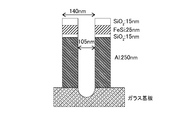
図7は、従来例である溝部の断面形状が四角形状である場合の偏光板の構成を模式的に示す断面図である。図7に示す偏光板は、ガラス基板と、ガラス基板上に141nmのピッチPで配列された幅W35nmのAlからなる反射層と、反射層上に配置された第1のSiO2層と、FeSi層と、第2のSiO2層とを備える。反射層の厚みT42は250nm、第1のSiO2層の厚みT43は5nm、第1のFeSi層の厚みT44は25nm、第2のSiO2層の厚みT45は15nmとした。また、FeSi層におけるFe含有量は5atm%、Si含有量は95atm%とした。
図7は、従来例である溝部の断面形状が四角形状である場合の偏光板の構成を模式的に示す断面図である。図7に示す偏光板は、ガラス基板と、ガラス基板上に141nmのピッチPで配列された幅W35nmのAlからなる反射層と、反射層上に配置された第1のSiO2層と、FeSi層と、第2のSiO2層とを備える。反射層の厚みT42は250nm、第1のSiO2層の厚みT43は5nm、第1のFeSi層の厚みT44は25nm、第2のSiO2層の厚みT45は15nmとした。また、FeSi層におけるFe含有量は5atm%、Si含有量は95atm%とした。
また、ガラス基板に形成された溝部の断面の形状を四角形とし、その深さをそれぞれ20nm、40nm、60nm、80nm、100nmとしてシミュレーションを行った。
表1に、従来例である溝部の断面形状を四角形状としたときの偏光板の各波長帯域の透過軸透過率Tp及び透過軸反射率Rpの平均値のシミュレーション結果を示す。

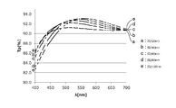
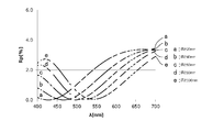
また、図8は、従来例である断面形状を四角形状とした溝部を所定深さにしたときの偏光板の透過軸透過率Tpのシミュレーション結果を示すグラフであり、図9は、従来例である断面形状を四角形状とした溝部を所定深さにしたときの偏光板の透過軸反射率Rpのシミュレーション結果を示すグラフである。
これらの結果より、溝部の断面形状を四角形状とした場合、青色波長帯域(波長430-510nm)の透過軸反射率Rpが大きく上昇し、光学特性が低下することが分かった。また、溝部の深さが60nm以上である場合、緑色波長帯域(波長520-590nm)の透過軸透過率Tpが低下し、青色波長帯域(波長430-510nm)の透過軸透過率Tpが、溝部の深さが0nmである場合よりも低下することが分かった。
[溝部の断面形状が略V字状]
図10は、溝部の断面形状が略V字状である場合の偏光板の構成を模式的に示す断面図である。図10に示す偏光板は、基板に凹設される溝部の断面形状を略V字状とした以外は、図7に示す偏光板の構成と同様とした。すなわち、この偏光板は、ガラス基板と、ガラス基板上に141nmのピッチPで配列された幅W35nmのAlからなる反射層と、反射層上に配置された第1のSiO2層と、FeSi層と、第2のSiO2層とを備える。反射層の厚みT52は250nm、第1のSiO2層の厚みT53は5nm、第1のFeSi層の厚みT54は25nm、第2のSiO2層の厚みT55は15nmとした。また、FeSi層におけるFe含有量は5atm%、Si含有量は95atm%とした。
図10は、溝部の断面形状が略V字状である場合の偏光板の構成を模式的に示す断面図である。図10に示す偏光板は、基板に凹設される溝部の断面形状を略V字状とした以外は、図7に示す偏光板の構成と同様とした。すなわち、この偏光板は、ガラス基板と、ガラス基板上に141nmのピッチPで配列された幅W35nmのAlからなる反射層と、反射層上に配置された第1のSiO2層と、FeSi層と、第2のSiO2層とを備える。反射層の厚みT52は250nm、第1のSiO2層の厚みT53は5nm、第1のFeSi層の厚みT54は25nm、第2のSiO2層の厚みT55は15nmとした。また、FeSi層におけるFe含有量は5atm%、Si含有量は95atm%とした。
また、ガラス基板に形成された溝部の断面の形状を略V字状の三角形とし、その深さをそれぞれ20nm、40nm、60nm、80nm、100nmとしてシミュレーションを行った。
表2に、溝部の断面形状を略V字状としたときの偏光板の各波長帯域の透過軸透過率Tp及び透過軸反射率Rpの平均値のシミュレーション結果を示す。
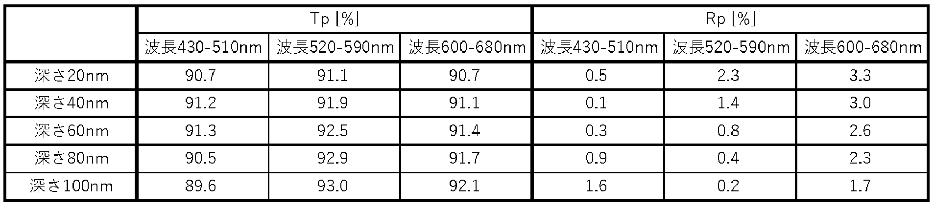
また、図11は、断面形状を略V字状とした溝部を所定深さにしたときの偏光板の透過軸透過率Tpのシミュレーション結果を示すグラフであり、図12は、断面形状を略V字状とした溝部を所定深さにしたときの偏光板の透過軸反射率Rpのシミュレーション結果を示すグラフである。
また、図13は、従来例である断面形状を四角形状とした溝部を所定深さにしたときの偏光板の各波長帯域の透過軸透過率Tpの平均値のシミュレーション結果を示すグラフであり、図14は、断面形状を略V字状とした溝部を所定深さにしたときの偏光板の各波長帯域の透過軸透過率Tpの平均値のシミュレーション結果を示すグラフである。
これらの結果より、溝部の断面形状を略V字状とした場合、緑色波長帯域(波長520-590nm)及び赤色波長帯域(波長600-680nm)において、透過軸透過率Tpを上昇させるとともに透過軸反射率Rpを低下させ、優れた光学特性が得られることが分かった。また、溝部の断面形状を略V字状とした場合、溝部の断面形状を四角形状とした場合に比して、青色波長帯域(波長430-510nm)の透過軸透過率Tpの低下を抑制させることが分かった。また、溝部の深さが60nm以上100nm以下である場合、青色波長帯域の透過軸透過率Tpが、溝部の深さが0nmである場合よりも大きくなり、優れた光学特性が得られることが分かった。
[溝部の断面形状が略U字状]
図15は、溝部の断面形状が略U字状である場合の偏光板の構成を模式的に示す断面図である。図15に示す偏光板は、基板に凹設される溝部の断面形状を略U字状とした以外は、図7に示す偏光板の構成と同様とした。すなわち、この偏光板は、ガラス基板と、ガラス基板上に141nmのピッチPで配列された幅W35nmのAlからなる反射層と、反射層上に配置された第1のSiO2層と、FeSi層と、第2のSiO2層とを備える。反射層の厚みT52は250nm、第1のSiO2層の厚みT53は5nm、第1のFeSi層の厚みT54は25nm、第2のSiO2層の厚みT55は15nmとした。また、FeSi層におけるFe含有量は5atm%、Si含有量は95atm%とした。
図15は、溝部の断面形状が略U字状である場合の偏光板の構成を模式的に示す断面図である。図15に示す偏光板は、基板に凹設される溝部の断面形状を略U字状とした以外は、図7に示す偏光板の構成と同様とした。すなわち、この偏光板は、ガラス基板と、ガラス基板上に141nmのピッチPで配列された幅W35nmのAlからなる反射層と、反射層上に配置された第1のSiO2層と、FeSi層と、第2のSiO2層とを備える。反射層の厚みT52は250nm、第1のSiO2層の厚みT53は5nm、第1のFeSi層の厚みT54は25nm、第2のSiO2層の厚みT55は15nmとした。また、FeSi層におけるFe含有量は5atm%、Si含有量は95atm%とした。
また、ガラス基板に形成された溝部の断面の形状を略U字状とし、その深さをそれぞれ20nm、40nm、60nm、80nm、100nm、120nmとしてシミュレーションを行った。
図16は、溝部の断面形状が略U字状である場合の溝部の構成を模式的に示す断面図であり、図17は、溝部の断面形状が略U字状である場合の溝部の断面形状の曲線を示すグラフである。
図16及び図17に示すように、溝部の断面形状は、溝部の深さゼロのときの幅の中点を原点(0,0)とし、グリッド間隔をW、溝の深さをDとしたとき、下記式を満たす2次曲線とした。
Y=(4D/W2)×X2-D
Y=(4D/W2)×X2-D
すなわち、図17に示すように、深さが20nm~120nmの溝部の断面形状の曲線(a)~(f)は、下記式とした。
(a)Y=0.007X2-20、(b)Y=0.015X2-40、(c)Y=0.022X2-60、(d)Y=0.029X2-80、(e)Y=0.036X2-100、(f)Y=0.044X2-120
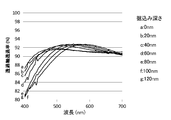
図18は、断面形状を略U字状とした溝部を所定深さにしたときの偏光板の透過軸透過率Tpのシミュレーション結果を示すグラフであり、図19は、断面形状を略U字状とした溝部を所定深さにしたときの偏光板の透過軸反射率Rpのシミュレーション結果を示すグラフである。
また、図20は、断面形状を略U字状とした溝部の深さに対する緑色波長帯域の透過軸透過率Tpの平均値のシミュレーション結果を示すグラフであり、図21は、断面形状を略U字状とした溝部の深さに対する緑色波長帯域の透過軸反射率Rpの平均値のシミュレーション結果を示すグラフである。
これらの結果より、溝部の断面形状を略U字状とした場合、緑色波長帯域(波長520-590nm)及び赤色波長帯域(波長600-680nm)において、透過軸透過率Tpを上昇させ、透過軸反射率Rpを低下させ、優れた光学特性が得られることが分かった。また、溝部の断面形状を略U字状とした場合、溝部の断面形状を四角形状とした場合に比して、青色波長帯域(波長430-510nm)の透過軸透過率Tpの低下を抑制させることが分かった。また、溝部の深さが60nm以上120nm以下である場合、緑色波長帯域の透過軸透過率Tpが大きく、緑色波長帯域の透過軸反射率Rpが小さいため、優れた光学特性が得られることが分かった。
[溝部の断面形状が略U字状(非対称)]
図22は、溝部の深さがゼロのときの幅の中点(原点)を通る垂線と、溝部の最深部と原点とを通る直線との角度の関係を示すグラフである。図22において、曲線(a)は、Y=0.036X2-100であり、曲線(b)は、溝部の深さがゼロのときの幅の中点(原点)を通る垂線と、原点と曲線(b)の最深部とを結んだ直線との角度が20°である曲線を示し、曲線(c)は、溝部の深さがゼロのときの幅の中点(原点)を通る垂線と、原点と曲線(b)の最深部とを結んだ直線との角度が-20°である曲線を示す。
図22は、溝部の深さがゼロのときの幅の中点(原点)を通る垂線と、溝部の最深部と原点とを通る直線との角度の関係を示すグラフである。図22において、曲線(a)は、Y=0.036X2-100であり、曲線(b)は、溝部の深さがゼロのときの幅の中点(原点)を通る垂線と、原点と曲線(b)の最深部とを結んだ直線との角度が20°である曲線を示し、曲線(c)は、溝部の深さがゼロのときの幅の中点(原点)を通る垂線と、原点と曲線(b)の最深部とを結んだ直線との角度が-20°である曲線を示す。
図22に示すように、溝部の断面形状を曲線(a)、曲線(b)、曲線(c)としたときの偏光板について、シミュレーションを行った。偏光板は、基板に凹設される溝部の断面形状を曲線(a)、曲線(b)、曲線(c)とした以外は、図15に示す偏光板の構成と同様とした。
図23は、溝部の断面形状を曲線(a)、曲線(b)、曲線(c)としたときの偏光板の透過軸透過率Tpのシミュレーション結果を示すグラフであり、図24は、溝部の断面形状を曲線(a)、曲線(b)、曲線(c)としたときの偏光板の透過軸反射率Rpのシミュレーション結果を示すグラフである。また、図25は、溝部の深さがゼロのときの幅の中点(原点)を通る垂線と、溝部の最深部と原点とを通る直線との角度がθのときの偏光板について、緑色波長帯域の透過軸透過率Tpの平均値のシミュレーション結果を示すグラフであり、図26は、溝部の深さがゼロのときの幅の中点(原点)を通る垂線と、溝部の最深部と原点とを通る直線との角度がθのときの偏光板について、緑色波長帯域の透過軸反射率Rpの平均値のシミュレーション結果を示すグラフである。
これらの結果より、溝部の深さがゼロのときの幅の中点(原点)を通る垂線と、溝部の最深部と原点とを通る直線との角度が±20°以下であることにより、溝部の最深部と原点とを通る直線との角度が0°の偏光板と同等の光学特性が得られることが分かった。
[溝部の断面形状の考察]
図27は、断面形状を四角形状、略V字状、又は略U字状とした溝部を所定深さにしたときの偏光板について、緑色波長帯域の透過軸透過率Tpの平均値のシミュレーション結果を示すグラフである。断面形状を四角形状、略V字状、又は略U字状とした溝部を有する偏光板は、それぞれ図7、図10、及び図15に示す偏光板と同様である。
図27は、断面形状を四角形状、略V字状、又は略U字状とした溝部を所定深さにしたときの偏光板について、緑色波長帯域の透過軸透過率Tpの平均値のシミュレーション結果を示すグラフである。断面形状を四角形状、略V字状、又は略U字状とした溝部を有する偏光板は、それぞれ図7、図10、及び図15に示す偏光板と同様である。
このシミュレーション結果より、溝部の深さを60nm以上100nm以下とすることにより、断面形状を四角形状とした溝部に比して、高い透過軸透過率Tpが得られることが分かった。
図28は、断面形状を四角形状、略V字状、又は略U字状とした溝部の深さ方向に対する屈折率のシミュレーション結果を示すグラフである。シミュレーションにおいて、空気の屈折率を1.0、基板の屈折率を1.5とし、ピッチを200nm、グリッド間幅を100nmとした。
深さが60nmの四角形状の溝部は、深さが0nmを超え60nm未満まで屈折率が1.25であり、深さが60nmのとき屈折率が1.5に大きく変化する変化点を有する。一方、深さが60nmの略V字状、又は略U字状の溝部は、幅が深さ方向に向かってゼロになるように小さくなるため、屈折率が1から1.5に徐々に変化し、屈折率の大きな変化点を持っていない。このように屈折率が大きな変化点を持たないように溝部を形成することにより、透過率特性及び反射率特性を向上させるものと考えられる。
深さが60nmの略V字状の溝部の深さに対する屈折率は、y=-0.0083x+1(-60≦x≦0)で示される。また、深さが100nmの略U字状の溝部の深さに対する屈折率は、y=2E-0.8x4+2E-06x3+0.0001x2-0.0004x+1.0061(-100≦x≦0)で示される。又は、深さが100nmの略U字状の溝部の深さに対する屈折率は、y=0.0005x2+0.0791x+4.423(-100≦x≦80)、y=2E-05x2+0.0021x+1.0026(-80≦x≦0)で示される。
よって、溝部の深さが0nm以上60nm以下の場合、y≦-0.0083x+1(-60≦x≦0)、y≧2E-0.8x4+2E-06x3+0.0001x2-0.0004x+1.0061(-60≦x≦0)を満たすように、溝部の断面の幅を深さ方向に向かってゼロになるように小さくすればよい。また、溝部の深さが60nm以上100nm以下の場合、1.5≧y≧2E-0.8x4+2E-06x3+0.0001x2-0.0004x+1.0061(-100≦x≦-60)を満たすように、溝部の断面の幅を深さ方向に向かってゼロになるように小さくすればよい。
11 透明基板、12 反射層、13 反射制御層、14A,14B,14C 溝部、 21 透明基板、22 反射層、23A 第1の誘電体層、23B 吸収層、23C 第2の誘電体層、31 透明基板、32 反射層、33 反射抑制層、41 透明基板、42 反射層、43 反射抑制層
Claims (11)
- 使用波長帯域の光に対して透明である透明基板と、
前記使用帯域の光の波長よりも短いピッチで前記透明基板上に配列され、所定方向に延在し、反射層と反射制御層とを有する格子状凸部と、
前記格子状凸部間に凹設され、前記所定方向に直交する方向の幅が深さ方向に向かってゼロになるように小さくなる溝部と
を備える偏光板。 - 前記溝部の前記所定方向に直交する方向の断面の形状が、略V字状である請求項1記載の偏光板。
- 前記溝部の前記所定方向に直交する方向の断面の形状が、略U字状である請求項1記載の偏光板。
- 前記溝部の所定方向に直交する方向の断面の形状は、溝部の深さゼロのときの幅の中点を通る垂線に対して非対称である請求項1乃至3のいずれか1項に記載の偏光板。
- 前記溝部の深さがゼロのときの幅の中点を通る垂線と、前記溝部の最深部と前記中点とを通る直線との角度が±20°以下である請求項1乃至3のいずれか1項に記載の偏光板
- 前記溝部の深さが、20nm以上100nm以下である請求項1乃至5のいずれか1項に記載の偏光板。
- 前記溝部の深さが、60nm以上100nm以下である請求項1乃至5のいずれか1項に記載の偏光板。
- 前記格子状凸部が、前記反射層と、誘電体層と、光吸収性材料からなる吸収層とがこの順に形成されてなる請求項1乃至7のいずれか1項に記載の偏光板。
- 前記格子状凸部が、前記反射層と、光吸収性材料と誘電体とが混合されてなる反射抑制層とがこの順に形成されてなる請求項1乃至7のいずれか1項に記載の偏光板。
- 前記請求項1乃至9のいずれか1項に記載の偏光板を搭載してなる光学機器。
- 使用波長帯域の光に対して透明である透明基板上に積層された反射層と反射制御層とをエッチングし、前記使用帯域の光の波長よりも短いピッチで配列され、所定方向に延在する格子状凸部と、前記格子状凸部間に凹設され、前記所定方向に直交する方向の幅が深さ方向に向かってゼロになるように小さくなる溝部とを形成する偏光板の製造方法。
Priority Applications (2)
| Application Number | Priority Date | Filing Date | Title |
|---|---|---|---|
| US16/627,638 US12235481B2 (en) | 2018-07-19 | 2019-07-12 | Polarizing plate |
| CN201980003256.9A CN110998384B (zh) | 2018-07-19 | 2019-07-12 | 偏振片 |
Applications Claiming Priority (2)
| Application Number | Priority Date | Filing Date | Title |
|---|---|---|---|
| JP2018-135721 | 2018-07-19 | ||
| JP2018135721A JP2018189980A (ja) | 2018-07-19 | 2018-07-19 | 偏光板 |
Publications (1)
| Publication Number | Publication Date |
|---|---|
| WO2020017455A1 true WO2020017455A1 (ja) | 2020-01-23 |
Family
ID=64480150
Family Applications (1)
| Application Number | Title | Priority Date | Filing Date |
|---|---|---|---|
| PCT/JP2019/027718 Ceased WO2020017455A1 (ja) | 2018-07-19 | 2019-07-12 | 偏光板 |
Country Status (4)
| Country | Link |
|---|---|
| US (1) | US12235481B2 (ja) |
| JP (2) | JP2018189980A (ja) |
| CN (1) | CN110998384B (ja) |
| WO (1) | WO2020017455A1 (ja) |
Families Citing this family (4)
| Publication number | Priority date | Publication date | Assignee | Title |
|---|---|---|---|---|
| US11150391B2 (en) * | 2018-11-30 | 2021-10-19 | Moxtek, Inc. | Flexible wire grid polarizer |
| JP7332324B2 (ja) * | 2019-04-10 | 2023-08-23 | デクセリアルズ株式会社 | 無機偏光板及びその製造方法、並びに光学機器 |
| JP7356291B2 (ja) * | 2019-08-23 | 2023-10-04 | デクセリアルズ株式会社 | 偏光板及び光学機器 |
| JP2024071147A (ja) * | 2022-11-14 | 2024-05-24 | デクセリアルズ株式会社 | ワイヤグリッド偏光素子およびその製造方法ならびに光学機器 |
Citations (7)
| Publication number | Priority date | Publication date | Assignee | Title |
|---|---|---|---|---|
| JP2003502708A (ja) * | 1999-06-22 | 2003-01-21 | モックステック | 可視スペクトル用の広帯域ワイヤグリッド偏光子 |
| JP2006330178A (ja) * | 2005-05-24 | 2006-12-07 | Sony Corp | 光学装置及び光学装置の製造方法 |
| JP2010085990A (ja) * | 2008-09-03 | 2010-04-15 | Asahi Kasei E-Materials Corp | ワイヤグリッド偏光板 |
| WO2013046921A1 (ja) * | 2011-09-27 | 2013-04-04 | 日本電気株式会社 | 偏光子、偏光光学素子、光源および画像表示装置 |
| JP2014186181A (ja) * | 2013-03-25 | 2014-10-02 | Seiko Epson Corp | 偏光素子の製造方法 |
| JP6312917B1 (ja) * | 2017-02-07 | 2018-04-18 | デクセリアルズ株式会社 | 無機偏光板及びその製造方法、並びに光学機器 |
| JP2018106129A (ja) * | 2016-12-28 | 2018-07-05 | デクセリアルズ株式会社 | 偏光板及びその製造方法、並びに光学機器 |
Family Cites Families (18)
| Publication number | Priority date | Publication date | Assignee | Title |
|---|---|---|---|---|
| US6288840B1 (en) * | 1999-06-22 | 2001-09-11 | Moxtek | Imbedded wire grid polarizer for the visible spectrum |
| WO2001094993A2 (en) * | 2000-06-08 | 2001-12-13 | Digital Reflection, Inc. | Reflective polarizer |
| JP2003344651A (ja) * | 2002-05-22 | 2003-12-03 | Nippon Sheet Glass Co Ltd | 薄膜構造体およびそれを用いた薄膜偏光子 |
| JP2006126338A (ja) | 2004-10-27 | 2006-05-18 | Nippon Sheet Glass Co Ltd | 偏光子およびその製造方法 |
| JP2007225744A (ja) * | 2006-02-22 | 2007-09-06 | Nippon Zeon Co Ltd | 偏光変換素子 |
| US20070217008A1 (en) * | 2006-03-17 | 2007-09-20 | Wang Jian J | Polarizer films and methods of making the same |
| JP4488033B2 (ja) | 2007-02-06 | 2010-06-23 | ソニー株式会社 | 偏光素子及び液晶プロジェクター |
| US20080316599A1 (en) * | 2007-06-22 | 2008-12-25 | Bin Wang | Reflection-Repressed Wire-Grid Polarizer |
| JP2009192586A (ja) * | 2008-02-12 | 2009-08-27 | Asahi Kasei E-Materials Corp | ワイヤグリッド型偏光素子及びそれを用いた表示装置 |
| KR100927587B1 (ko) * | 2008-04-30 | 2009-11-23 | 삼성모바일디스플레이주식회사 | 액정 표시 장치 |
| JP5760388B2 (ja) * | 2010-11-01 | 2015-08-12 | セイコーエプソン株式会社 | 偏光素子とその製造方法、プロジェクター、液晶装置、電子機器 |
| JP5796522B2 (ja) * | 2012-03-23 | 2015-10-21 | セイコーエプソン株式会社 | 偏光素子、および偏光素子の製造方法 |
| CN102681078B (zh) * | 2012-06-06 | 2014-09-24 | 昆山龙腾光电有限公司 | 光栅偏振片 |
| JP6100492B2 (ja) | 2012-09-05 | 2017-03-22 | デクセリアルズ株式会社 | 偏光素子、プロジェクター及び偏光素子の製造方法 |
| JP6285131B2 (ja) | 2013-07-10 | 2018-02-28 | デクセリアルズ株式会社 | 偏光板、及び偏光板の製造方法 |
| JP2015219319A (ja) * | 2014-05-15 | 2015-12-07 | デクセリアルズ株式会社 | 無機偏光板及びその製造方法 |
| JP5996587B2 (ja) * | 2014-08-22 | 2016-09-21 | デクセリアルズ株式会社 | 無機偏光板及びその製造方法 |
| JP6230689B1 (ja) * | 2016-12-28 | 2017-11-15 | デクセリアルズ株式会社 | 偏光板及びその製造方法、並びに光学機器 |
-
2018
- 2018-07-19 JP JP2018135721A patent/JP2018189980A/ja active Pending
-
2019
- 2019-07-12 CN CN201980003256.9A patent/CN110998384B/zh active Active
- 2019-07-12 US US16/627,638 patent/US12235481B2/en active Active
- 2019-07-12 WO PCT/JP2019/027718 patent/WO2020017455A1/ja not_active Ceased
-
2023
- 2023-03-13 JP JP2023038233A patent/JP7531645B2/ja active Active
Patent Citations (7)
| Publication number | Priority date | Publication date | Assignee | Title |
|---|---|---|---|---|
| JP2003502708A (ja) * | 1999-06-22 | 2003-01-21 | モックステック | 可視スペクトル用の広帯域ワイヤグリッド偏光子 |
| JP2006330178A (ja) * | 2005-05-24 | 2006-12-07 | Sony Corp | 光学装置及び光学装置の製造方法 |
| JP2010085990A (ja) * | 2008-09-03 | 2010-04-15 | Asahi Kasei E-Materials Corp | ワイヤグリッド偏光板 |
| WO2013046921A1 (ja) * | 2011-09-27 | 2013-04-04 | 日本電気株式会社 | 偏光子、偏光光学素子、光源および画像表示装置 |
| JP2014186181A (ja) * | 2013-03-25 | 2014-10-02 | Seiko Epson Corp | 偏光素子の製造方法 |
| JP2018106129A (ja) * | 2016-12-28 | 2018-07-05 | デクセリアルズ株式会社 | 偏光板及びその製造方法、並びに光学機器 |
| JP6312917B1 (ja) * | 2017-02-07 | 2018-04-18 | デクセリアルズ株式会社 | 無機偏光板及びその製造方法、並びに光学機器 |
Also Published As
| Publication number | Publication date |
|---|---|
| CN110998384B (zh) | 2023-04-07 |
| US12235481B2 (en) | 2025-02-25 |
| US20210302639A1 (en) | 2021-09-30 |
| JP2018189980A (ja) | 2018-11-29 |
| JP2023076488A (ja) | 2023-06-01 |
| CN110998384A (zh) | 2020-04-10 |
| JP7531645B2 (ja) | 2024-08-09 |
Similar Documents
| Publication | Publication Date | Title |
|---|---|---|
| US11543702B2 (en) | Polarizer and optical apparatus | |
| JP7531645B2 (ja) | 偏光板 | |
| JP4488033B2 (ja) | 偏光素子及び液晶プロジェクター | |
| JP6302040B1 (ja) | 偏光板及びその製造方法、並びに光学機器 | |
| CN107407770A (zh) | 偏振元件 | |
| JP6722832B2 (ja) | 偏光板及びこれを備える光学機器 | |
| JP6577641B2 (ja) | 偏光板及びその製造方法、並びに光学機器 | |
| US11630254B2 (en) | Wire grid polarizing plate having trapezoidal absorption layer | |
| JP6484373B1 (ja) | 偏光板及びこれを備える光学機器 | |
| US11971568B2 (en) | Polarizing plate, manufacturing method thereof, and optical device | |
| JP6703050B2 (ja) | 偏光板、光学機器及び偏光板の製造方法 | |
| JP6935318B2 (ja) | 偏光板及びその製造方法、並びに光学機器 | |
| US11543573B2 (en) | Polarizing plate and optical apparatus containing same | |
| WO2020022433A1 (ja) | 偏光板及び光学機器 | |
| US11644605B2 (en) | Polarizing element having alternately laminated dielectric layers and conductive layers and method for manufacturing polarizing element | |
| JP2020086426A (ja) | 偏光板及びそれを備えた光学機器 | |
| JP2020003771A (ja) | 偏光板の製造方法 | |
| JP7075372B2 (ja) | 偏光板及びその製造方法、並びに光学機器 |
Legal Events
| Date | Code | Title | Description |
|---|---|---|---|
| 121 | Ep: the epo has been informed by wipo that ep was designated in this application |
Ref document number: 19838321 Country of ref document: EP Kind code of ref document: A1 |
|
| NENP | Non-entry into the national phase |
Ref country code: DE |
|
| 122 | Ep: pct application non-entry in european phase |
Ref document number: 19838321 Country of ref document: EP Kind code of ref document: A1 |
|
| WWG | Wipo information: grant in national office |
Ref document number: 16627638 Country of ref document: US |