WO2020004091A1 - プラズマ処理装置、プラズマ状態検出方法およびプラズマ状態検出プログラム - Google Patents
プラズマ処理装置、プラズマ状態検出方法およびプラズマ状態検出プログラム Download PDFInfo
- Publication number
- WO2020004091A1 WO2020004091A1 PCT/JP2019/023793 JP2019023793W WO2020004091A1 WO 2020004091 A1 WO2020004091 A1 WO 2020004091A1 JP 2019023793 W JP2019023793 W JP 2019023793W WO 2020004091 A1 WO2020004091 A1 WO 2020004091A1
- Authority
- WO
- WIPO (PCT)
- Prior art keywords
- heater
- plasma
- temperature
- state
- wafer
- Prior art date
- Legal status (The legal status is an assumption and is not a legal conclusion. Google has not performed a legal analysis and makes no representation as to the accuracy of the status listed.)
- Ceased
Links
Images


Classifications
-
- H—ELECTRICITY
- H01—ELECTRIC ELEMENTS
- H01J—ELECTRIC DISCHARGE TUBES OR DISCHARGE LAMPS
- H01J37/00—Discharge tubes with provision for introducing objects or material to be exposed to the discharge, e.g. for the purpose of examination or processing thereof
- H01J37/32—Gas-filled discharge tubes
- H01J37/32917—Plasma diagnostics
- H01J37/32935—Monitoring and controlling tubes by information coming from the object and/or discharge
-
- H—ELECTRICITY
- H01—ELECTRIC ELEMENTS
- H01J—ELECTRIC DISCHARGE TUBES OR DISCHARGE LAMPS
- H01J37/00—Discharge tubes with provision for introducing objects or material to be exposed to the discharge, e.g. for the purpose of examination or processing thereof
- H01J37/32—Gas-filled discharge tubes
-
- G—PHYSICS
- G05—CONTROLLING; REGULATING
- G05D—SYSTEMS FOR CONTROLLING OR REGULATING NON-ELECTRIC VARIABLES
- G05D23/00—Control of temperature
- G05D23/19—Control of temperature characterised by the use of electric means
- G05D23/1917—Control of temperature characterised by the use of electric means using digital means
-
- G—PHYSICS
- G05—CONTROLLING; REGULATING
- G05D—SYSTEMS FOR CONTROLLING OR REGULATING NON-ELECTRIC VARIABLES
- G05D23/00—Control of temperature
- G05D23/19—Control of temperature characterised by the use of electric means
- G05D23/1927—Control of temperature characterised by the use of electric means using a plurality of sensors
- G05D23/193—Control of temperature characterised by the use of electric means using a plurality of sensors sensing the temperaure in different places in thermal relationship with one or more spaces
-
- G—PHYSICS
- G08—SIGNALLING
- G08B—SIGNALLING SYSTEMS, e.g. PERSONAL CALLING SYSTEMS; ORDER TELEGRAPHS; ALARM SYSTEMS
- G08B21/00—Alarms responsive to a single specified undesired or abnormal condition and not otherwise provided for
- G08B21/18—Status alarms
-
- H—ELECTRICITY
- H01—ELECTRIC ELEMENTS
- H01J—ELECTRIC DISCHARGE TUBES OR DISCHARGE LAMPS
- H01J37/00—Discharge tubes with provision for introducing objects or material to be exposed to the discharge, e.g. for the purpose of examination or processing thereof
- H01J37/32—Gas-filled discharge tubes
- H01J37/32431—Constructional details of the reactor
- H01J37/32715—Workpiece holder
- H01J37/32724—Temperature
-
- H—ELECTRICITY
- H01—ELECTRIC ELEMENTS
- H01J—ELECTRIC DISCHARGE TUBES OR DISCHARGE LAMPS
- H01J37/00—Discharge tubes with provision for introducing objects or material to be exposed to the discharge, e.g. for the purpose of examination or processing thereof
- H01J37/32—Gas-filled discharge tubes
- H01J37/32917—Plasma diagnostics
- H01J37/32926—Software, data control or modelling
-
- H—ELECTRICITY
- H01—ELECTRIC ELEMENTS
- H01J—ELECTRIC DISCHARGE TUBES OR DISCHARGE LAMPS
- H01J37/00—Discharge tubes with provision for introducing objects or material to be exposed to the discharge, e.g. for the purpose of examination or processing thereof
- H01J37/32—Gas-filled discharge tubes
- H01J37/32917—Plasma diagnostics
- H01J37/32935—Monitoring and controlling tubes by information coming from the object and/or discharge
- H01J37/32944—Arc detection
-
- H—ELECTRICITY
- H01—ELECTRIC ELEMENTS
- H01J—ELECTRIC DISCHARGE TUBES OR DISCHARGE LAMPS
- H01J37/00—Discharge tubes with provision for introducing objects or material to be exposed to the discharge, e.g. for the purpose of examination or processing thereof
- H01J37/32—Gas-filled discharge tubes
- H01J37/32917—Plasma diagnostics
- H01J37/3299—Feedback systems
-
- H—ELECTRICITY
- H05—ELECTRIC TECHNIQUES NOT OTHERWISE PROVIDED FOR
- H05B—ELECTRIC HEATING; ELECTRIC LIGHT SOURCES NOT OTHERWISE PROVIDED FOR; CIRCUIT ARRANGEMENTS FOR ELECTRIC LIGHT SOURCES, IN GENERAL
- H05B1/00—Details of electric heating devices
- H05B1/02—Automatic switching arrangements specially adapted to apparatus ; Control of heating devices
- H05B1/0227—Applications
- H05B1/023—Industrial applications
- H05B1/0233—Industrial applications for semiconductors manufacturing
-
- H—ELECTRICITY
- H05—ELECTRIC TECHNIQUES NOT OTHERWISE PROVIDED FOR
- H05H—PLASMA TECHNIQUE; PRODUCTION OF ACCELERATED ELECTRICALLY-CHARGED PARTICLES OR OF NEUTRONS; PRODUCTION OR ACCELERATION OF NEUTRAL MOLECULAR OR ATOMIC BEAMS
- H05H1/00—Generating plasma; Handling plasma
- H05H1/0006—Investigating plasma, e.g. measuring the degree of ionisation or the electron temperature
- H05H1/0081—Investigating plasma, e.g. measuring the degree of ionisation or the electron temperature by electric means
-
- H—ELECTRICITY
- H10—SEMICONDUCTOR DEVICES; ELECTRIC SOLID-STATE DEVICES NOT OTHERWISE PROVIDED FOR
- H10P—GENERIC PROCESSES OR APPARATUS FOR THE MANUFACTURE OR TREATMENT OF DEVICES COVERED BY CLASS H10
- H10P50/00—Etching of wafers, substrates or parts of devices
- H10P50/20—Dry etching; Plasma etching; Reactive-ion etching
- H10P50/24—Dry etching; Plasma etching; Reactive-ion etching of semiconductor materials
- H10P50/242—Dry etching; Plasma etching; Reactive-ion etching of semiconductor materials of Group IV materials
-
- H—ELECTRICITY
- H01—ELECTRIC ELEMENTS
- H01J—ELECTRIC DISCHARGE TUBES OR DISCHARGE LAMPS
- H01J2237/00—Discharge tubes exposing object to beam, e.g. for analysis treatment, etching, imaging
- H01J2237/245—Detection characterised by the variable being measured
- H01J2237/24571—Measurements of non-electric or non-magnetic variables
- H01J2237/24585—Other variables, e.g. energy, mass, velocity, time, temperature
-
- H—ELECTRICITY
- H01—ELECTRIC ELEMENTS
- H01J—ELECTRIC DISCHARGE TUBES OR DISCHARGE LAMPS
- H01J2237/00—Discharge tubes exposing object to beam, e.g. for analysis treatment, etching, imaging
- H01J2237/32—Processing objects by plasma generation
- H01J2237/33—Processing objects by plasma generation characterised by the type of processing
- H01J2237/334—Etching
- H01J2237/3341—Reactive etching
-
- H—ELECTRICITY
- H05—ELECTRIC TECHNIQUES NOT OTHERWISE PROVIDED FOR
- H05B—ELECTRIC HEATING; ELECTRIC LIGHT SOURCES NOT OTHERWISE PROVIDED FOR; CIRCUIT ARRANGEMENTS FOR ELECTRIC LIGHT SOURCES, IN GENERAL
- H05B2203/00—Aspects relating to Ohmic resistive heating covered by group H05B3/00
- H05B2203/002—Heaters using a particular layout for the resistive material or resistive elements
- H05B2203/005—Heaters using a particular layout for the resistive material or resistive elements using multiple resistive elements or resistive zones isolated from each other
-
- H—ELECTRICITY
- H05—ELECTRIC TECHNIQUES NOT OTHERWISE PROVIDED FOR
- H05H—PLASMA TECHNIQUE; PRODUCTION OF ACCELERATED ELECTRICALLY-CHARGED PARTICLES OR OF NEUTRONS; PRODUCTION OR ACCELERATION OF NEUTRAL MOLECULAR OR ATOMIC BEAMS
- H05H1/00—Generating plasma; Handling plasma
- H05H1/24—Generating plasma
- H05H1/46—Generating plasma using applied electromagnetic fields, e.g. high frequency or microwave energy
Definitions
- the present disclosure relates to a plasma processing apparatus, a plasma state detection method, and a plasma state detection program.
- JP 2009-194032 A JP 2009-087790 A JP 2014-513390A
- the present disclosure provides a technology for detecting a state of plasma without disposing a sensor.
- a plasma processing apparatus includes a mounting table, a heater control unit, a measurement unit, a parameter calculation unit, and an output unit.
- the mounting table is provided with a heater capable of adjusting the temperature of a mounting surface on which an object to be processed to be subjected to plasma processing is mounted.
- the heater control unit controls the power supplied to the heater so that the heater has a set temperature.
- the measuring unit controls the power supplied to the heater by the heater control unit so that the temperature of the heater is constant, so that the plasma is not ignited and the power supplied to the heater after the plasma is ignited. Measure the supply power in the falling transient state.
- the parameter calculation unit includes a heat input amount from the plasma as a parameter, and performs a fitting using a supply model in the unignited state and the transition state measured by the measurement unit with respect to a calculation model for calculating the supply state in the transient state. To calculate the heat input.
- the output unit outputs information based on the heat input amount calculated by the parameter calculation unit.
- the state of plasma can be detected without disposing a sensor in the processing container.
- FIG. 1 is a cross-sectional view illustrating an example of a schematic configuration of a plasma processing apparatus according to an embodiment.
- FIG. 2 is a plan view illustrating an example of the configuration of the mounting table according to the embodiment.
- FIG. 3 is a block diagram illustrating an example of a schematic configuration of a control unit that controls the plasma processing apparatus according to the embodiment.
- FIG. 4 is a diagram schematically illustrating an example of the flow of energy affecting the temperature of the wafer.
- FIG. 5A is a diagram schematically illustrating an example of the flow of energy in an unignited state.
- FIG. 5B is a diagram schematically illustrating an example of the flow of energy in the ignition state.
- FIG. 5A is a diagram schematically illustrating an example of the flow of energy in an unignited state.
- FIG. 5B is a diagram schematically illustrating an example of the flow of energy in the ignition state.
- FIG. 6 is a diagram illustrating an example of a change in the temperature of the wafer W and the power supplied to the heater HT.
- FIG. 7 is a diagram schematically illustrating an example of the flow of energy in the ignition state.
- FIG. 8 is a diagram schematically illustrating an example of a temperature change between an unignited state and a transient state due to a plasma density distribution.
- FIG. 9 is a diagram schematically illustrating an example of an energy flow in an unignited state and a transient state.
- FIG. 10 is a diagram illustrating an example of a change in the temperature of the wafer W and the power supplied to the heater HT.
- FIG. 11A is a diagram illustrating an example of output of information indicating a plasma density distribution.
- FIG. 11A is a diagram illustrating an example of output of information indicating a plasma density distribution.
- FIG. 11B is a diagram illustrating an example of output of information indicating a plasma density distribution.
- FIG. 12 is a diagram schematically illustrating plasma etching.
- FIG. 13 is a flowchart illustrating an example of the flow of plasma state detection and plasma state control according to the embodiment.
- FIG. 14 is a plan view illustrating an example of division of the mounting surface of the mounting table according to the embodiment.
- a plasma processing apparatus in which sensors such as various probes and various electric sensors are arranged in a processing chamber to detect a state of plasma.
- sensors such as various probes and various electric sensors are arranged in a processing chamber to detect a state of plasma.
- the sensor is disposed in the processing vessel, sometimes at a location near the plasma generation region, the state of the plasma changes due to the influence of the sensor. Then, in the plasma processing apparatus, there is a concern that the characteristics and uniformity of the plasma processing for the film to be processed may be affected. In the plasma processing apparatus, there is a concern that particles or abnormal discharge may occur.
- plasma processing apparatus when a sensor is disposed in a processing container, plasma processing may not be performed on a target film in some cases. Then, the plasma processing apparatus cannot detect the state of the plasma during the actual plasma processing. Therefore, it is expected that the state of plasma is detected without disposing a sensor in the processing container.
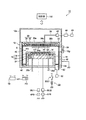
- FIG. 1 is a cross-sectional view illustrating an example of a schematic configuration of a plasma processing apparatus according to an embodiment.
- the plasma processing apparatus 10 shown in FIG. 1 is a capacitively coupled parallel plate plasma etching apparatus.
- the plasma processing apparatus 10 includes a substantially cylindrical processing container 12.
- the processing container 12 is made of, for example, aluminum.
- the surface of the processing container 12 is subjected to an anodizing treatment.
- a mounting table 16 is provided in the processing container 12.
- the mounting table 16 includes an electrostatic chuck 18 and a base 20.
- the upper surface of the electrostatic chuck 18 is a mounting surface on which an object to be processed to be subjected to plasma processing is mounted.
- a wafer W is placed on the upper surface of the electrostatic chuck 18 as an object to be processed.
- the base 20 has a substantially disc shape, and its main part is made of a conductive metal such as aluminum.
- the base 20 constitutes a lower electrode.
- the base 20 is supported by the support unit 14.
- the support portion 14 is a cylindrical member extending from the bottom of the processing container 12.
- the first high-frequency power supply HFS is electrically connected to the base 20.
- the first high-frequency power supply HFS is a power supply that generates high-frequency power for plasma generation, and generates a high-frequency power of 27 to 100 MHz, for example, 40 MHz.
- the matching unit MU1 has a circuit for matching the output impedance of the first high-frequency power supply HFS with the input impedance on the load side (base 20 side).
- the second high frequency power supply LFS is electrically connected to the base 20 via the matching unit MU2.
- the second high-frequency power supply LFS generates high-frequency power (high-frequency bias power) for attracting ions to the wafer W, and supplies the high-frequency bias power to the base 20. As a result, a bias potential is generated on the base 20.
- the frequency of the high frequency bias power is a frequency in the range of 400 kHz to 13.56 MHz, and is 3 MHz in one example.
- the matching unit MU2 has a circuit for matching the output impedance of the second high-frequency power supply LFS with the input impedance on the load side (the base 20 side).
- the electrostatic chuck 18 is provided on the base 20.
- the electrostatic chuck 18 attracts the wafer W by electrostatic force such as Coulomb force and holds the wafer W.
- the electrostatic chuck 18 has an electrode E1 for electrostatic attraction in a ceramic main body.
- a DC power supply 22 is electrically connected to the electrode E1 via a switch SW1.
- the suction force for holding the wafer W depends on the value of the DC voltage applied from the DC power supply 22.
- a focus ring FR is provided on the upper surface of the base 20 and around the electrostatic chuck 18.
- the focus ring FR is provided to improve the uniformity of the plasma processing.
- the focus ring FR is made of a material appropriately selected according to the plasma processing to be performed, and may be made of, for example, silicon or quartz.
- a coolant channel 24 is formed inside the base 20.
- a coolant is supplied to the coolant channel 24 from a chiller unit provided outside the processing container 12 via a pipe 26a.
- the refrigerant supplied to the refrigerant flow path 24 returns to the chiller unit via the pipe 26b.
- An upper electrode 30 is provided in the processing container 12.
- the upper electrode 30 is disposed above the mounting table 16 so as to face the base 20, and the base 20 and the upper electrode 30 are provided substantially parallel to each other.
- the upper electrode 30 is supported on the upper part of the processing container 12 via the insulating shielding member 32.
- the upper electrode 30 may include an electrode plate 34 and an electrode support 36.
- the electrode plate 34 faces the processing space S and provides a plurality of gas discharge holes 34a.
- the electrode plate 34 can be made of a low-resistance conductor or semiconductor having low Joule heat.
- the electrode support 36 supports the electrode plate 34 in a detachable manner, and may be made of a conductive material such as aluminum.
- the electrode support 36 may have a water-cooled structure. Inside the electrode support 36, a gas diffusion chamber 36a is provided. A plurality of gas flow holes 36b communicating with the gas discharge holes 34a extend downward from the gas diffusion chamber 36a.
- the electrode support 36 has a gas inlet 36c for guiding the processing gas to the gas diffusion chamber 36a, and a gas supply pipe 38 is connected to the gas inlet 36c.
- a gas source group 40 is connected to the gas supply pipe 38 via a valve group 42 and a flow controller group 44.
- the valve group 42 has a plurality of open / close valves
- the flow controller group 44 has a plurality of flow controllers such as a mass flow controller.
- the gas source group 40 has gas sources for a plurality of types of gases required for the plasma processing.
- the plurality of gas sources of the gas source group 40 are connected to the gas supply pipe 38 via the corresponding open / close valve and the corresponding mass flow controller.
- one or more gases from one or more gas sources selected from a plurality of gas sources in the gas source group 40 are supplied to the gas supply pipe.
- the gas supplied to the gas supply pipe 38 reaches the gas diffusion chamber 36a, and is discharged into the processing space S via the gas flow holes 36b and the gas discharge holes 34a.
- the plasma processing apparatus 10 may further include a ground conductor 12a.
- the ground conductor 12 a is a substantially cylindrical ground conductor, and is provided so as to extend from the side wall of the processing container 12 to a position higher than the height position of the upper electrode 30.
- a deposition shield 46 is detachably provided along the inner wall of the processing container 12.
- the deposition shield 46 is also provided on the outer periphery of the support portion 14.
- the deposition shield 46 prevents etching by-products (deposition) from adhering to the processing container 12, and can be configured by coating an aluminum material with ceramic such as Y 2 O 3 .
- an exhaust plate 48 is provided between the support portion 14 and the inner wall of the processing container 12.
- the exhaust plate 48 can be configured by, for example, coating an aluminum material with a ceramic such as Y 2 O 3 .
- An exhaust port 12 e is provided in the processing container 12 below the exhaust plate 48.
- An exhaust device 50 is connected to the exhaust port 12e via an exhaust pipe 52.
- the exhaust device 50 has a vacuum pump such as a turbo molecular pump, and can reduce the pressure inside the processing container 12 to a desired degree of vacuum.
- a loading / unloading port 12g for the wafer W is provided on a side wall of the processing container 12, and the loading / unloading port 12g can be opened and closed by a gate valve 54.
- the operation of the plasma processing apparatus 10 configured as described above is totally controlled by the control unit 100.
- the control unit 100 is, for example, a computer and controls each unit of the plasma processing apparatus 10.
- the operation of the plasma processing apparatus 10 is totally controlled by the control unit 100.
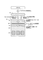
- FIG. 2 is a plan view illustrating an example of the configuration of the mounting table according to the embodiment.
- the mounting table 16 has the electrostatic chuck 18 and the base 20.
- the electrostatic chuck 18 has a main body 18m made of ceramic.
- the main body 18m has a substantially disk shape.
- the main body 18m provides a mounting area 18a and an outer peripheral area 18b.
- the mounting area 18a is a substantially circular area in plan view.
- the wafer W is mounted on the upper surface of the mounting area 18a. That is, the upper surface of the mounting area 18a functions as a mounting surface on which the wafer W is mounted.
- the diameter of the mounting area 18a is substantially the same as the diameter of the wafer W, or is slightly smaller than the diameter of the wafer W.
- the outer peripheral area 18b is an area surrounding the mounting area 18a, and extends in a substantially annular shape. In the present embodiment, the upper surface of the outer peripheral region 18b is at a position lower than the upper surface of the mounting region 18a.
- the electrostatic chuck 18 has an electrode E1 for electrostatic attraction in the mounting area 18a.
- the electrode E1 is connected to the DC power supply 22 via the switch SW1, as described above.
- a plurality of heaters HT are provided in the mounting area 18a and below the electrode E1.
- the mounting area 18a is divided into a plurality of divided areas, and a heater HT is provided in each of the divided areas.
- a plurality of heaters HT are provided in a central circular region of the mounting region 18a and in a plurality of concentric annular regions surrounding the circular region. In each of the plurality of annular regions, a plurality of heaters HT are arranged in the circumferential direction. Note that the division method of the division region shown in FIG. 2 is an example, and the present invention is not limited to this.
- the mounting area 18a may be divided into more divided areas.
- the placement area 18a may be divided into divided areas having a smaller angular width and a smaller radial width as it approaches the outer periphery.
- the heaters HT are individually connected to a heater power supply HP shown in FIG. 1 via wiring (not shown) provided on the outer peripheral portion of the base 20.
- the heater power supply HP supplies electric power adjusted individually to each heater HT under the control of the control unit 100. Accordingly, the heat generated by each heater HT is individually controlled, and the temperatures of the plurality of divided regions in the placement region 18a are individually adjusted.
- the heater power supply HP is provided with a power detection unit PD that detects power supplied to each heater HT.
- the power detection unit PD may be provided separately from the heater power supply HP on a wire through which power flows from the heater power supply HP to each heater HT.
- the power detection unit PD detects power supplied to each heater HT.
- the power detection unit PD detects a power amount [W] as a supply power supplied to each heater HT.
- the heater HT generates heat according to the amount of electric power. Therefore, the amount of power supplied to the heater HT indicates the heater power.
- the power detection unit PD notifies the control unit 100 of power data indicating the detected power supply to each heater HT.
- the mounting table 16 is provided with a temperature sensor (not shown) that can detect the temperature of the heater HT in each of the divided areas of the mounting area 18a.
- the temperature sensor may be an element that can measure the temperature separately from the heater HT.
- the temperature sensor is disposed on a wiring through which electric power flows to the heater HT, and utilizes the fact that the electrical resistance of the main metal increases in proportion to the temperature rise, thereby making it possible to measure the voltage and current applied to the heater HT.
- the temperature may be detected from the resistance value obtained from the measurement.
- the sensor value detected by each temperature sensor is sent to a temperature measuring device TD.
- the temperature measuring device TD measures the temperature of each divided region of the mounting region 18a from each sensor value.
- the temperature measuring device TD notifies the control unit 100 of temperature data indicating the temperature of each divided region of the mounting region 18a.
- a heat transfer gas for example, a He gas may be supplied between the upper surface of the electrostatic chuck 18 and the back surface of the wafer W by a heat transfer gas supply mechanism and a gas supply line (not shown).
- FIG. 3 is a block diagram illustrating an example of a schematic configuration of a control unit that controls the plasma processing apparatus according to the embodiment.
- the control unit 100 includes an external interface 101, a process controller 102, a user interface 103, and a storage unit 104.
- the external interface 101 can communicate with each unit of the plasma processing apparatus 10 and inputs and outputs various data. For example, power data indicating power supplied from the power detection unit PD to each heater HT is input to the external interface 101. Further, temperature data indicating the temperature of each divided area of the mounting area 18a is input to the external interface 101 from the temperature measuring device TD. Further, the external interface 101 outputs control data for controlling the power supplied to each heater HT to the heater power supply HP.
- the process controller 102 includes a CPU (Central Processing Unit) and controls each unit of the plasma processing apparatus 10.
- CPU Central Processing Unit
- the user interface 103 includes a keyboard for a process manager to input commands for managing the plasma processing apparatus 10, a display for visualizing and displaying the operation status of the plasma processing apparatus 10, and the like.
- the storage unit 104 stores a control program (software) for realizing various processes executed by the plasma processing apparatus 10 under the control of the process controller 102, a recipe storing processing condition data and the like, and a plasma process.
- the parameters and the like regarding the devices and processes for performing are stored.
- recipes such as control programs and processing condition data are stored in a computer-readable medium (eg, an optical disk such as a hard disk or a DVD, a flexible disk, a semiconductor memory, or the like), and are stored in a computer-readable medium. Is also good.
- the recipe can be transmitted from another device as needed, for example, via a dedicated line and used online.
- the process controller 102 has an internal memory for storing programs and data, reads out the control program stored in the storage unit 104, and executes processing of the read out control program.
- the process controller 102 functions as various processing units when the control program operates.
- the process controller 102 has functions of a heater control unit 102a, a measurement unit 102b, a parameter calculation unit 102c, an output unit 102d, an alert unit 102e, a change unit 102f, and a set temperature calculation unit 102g.
- each function of the heater control unit 102a, the measurement unit 102b, the parameter calculation unit 102c, the output unit 102d, the alert unit 102e, the change unit 102f, and the set temperature calculation unit 102g may be implemented in a distributed manner by a plurality of controllers. .
- FIG. 4 is a diagram schematically illustrating an example of the flow of energy affecting the temperature of the wafer.
- FIG. 4 shows the mounting table 16 including the wafer W and the electrostatic chuck (ESC) 18 in a simplified manner.
- the example of FIG. 4 shows the flow of energy that affects the temperature of the wafer W in one divided area of the mounting area 18a of the electrostatic chuck 18.
- the mounting table 16 has an electrostatic chuck 18 and a base 20.
- the electrostatic chuck 18 and the base 20 are adhered by an adhesive layer 19.
- a heater HT is provided inside the mounting area 18a of the electrostatic chuck 18.
- a coolant passage 24 through which the coolant flows is formed.
- the heater HT generates heat according to the power supplied from the heater power supply HP, and the temperature rises.
- FIG. 4 shows the supply power supplied to the heater HT as the heater power P h.
- the heater power P h the amount of heat generated per unit area heater HT is divided by the area A of the area provided for the electrostatic chuck 18 (heat flux) q h occurs.
- FIG. 4 shows the heat input from the plasma to the wafer W as a heat flux q p from the plasma per unit area divided by the area of the wafer W.
- the heat input from the plasma is mainly proportional to the product of the amount of ions in the plasma applied to the wafer W and the bias potential for drawing the ions in the plasma into the wafer W.
- the amount of ions in the plasma applied to the wafer W is proportional to the electron density of the plasma.
- the electron density of the plasma is proportional to the power of the high-frequency power HFS from the first high-frequency power supply HFS applied to generate the plasma. Further, the electron density of the plasma depends on the pressure in the processing chamber 12.
- the bias potential for drawing ions in the plasma into the wafer W is proportional to the power of the high-frequency power LFS from the second high-frequency power supply LFS applied when the bias potential is generated.
- the bias potential for drawing ions in the plasma to the wafer W depends on the pressure in the processing chamber 12.
- ions are drawn into the mounting table due to a potential difference between the plasma (plasma potential) generated when the plasma is generated and the mounting table 12.
- the heat input from the plasma includes heating by plasma emission, irradiation of the wafer W by electrons and radicals in the plasma, and surface reaction on the wafer W by ions and radicals. These components also depend on the power and pressure of the AC power.
- the heat input from the plasma depends on other device parameters related to plasma generation, for example, the distance between the mounting table 16 and the upper electrode 30 and the type of gas supplied to the processing space S.
- the heat transmitted to the wafer W is transmitted to the electrostatic chuck 18.
- heat is transmitted to the electrostatic chuck 18 according to the degree of difficulty in transmitting heat, such as the degree of contact between the wafer W and the electrostatic chuck 18.
- the difficulty in conducting heat that is, the thermal resistance
- R th ⁇ A per unit area between the wafer W and the surface of the electrostatic chuck 18.
- A is the area of the region where the heater HT is provided.
- Rth is the thermal resistance in the entire area where the heater HT is provided. Further, in FIG. 4, the amount of heat input from the wafer W to the surface of the electrostatic chuck 18 is shown as a heat flux q per unit area from the wafer W to the surface of the electrostatic chuck 18.
- the thermal resistance R th ⁇ A per unit area between the wafer W and the surface of the electrostatic chuck 18 is the surface state of the electrostatic chuck 18 and the DC voltage applied from the DC power supply 22 for holding the wafer W. And the pressure of the heat transfer gas supplied between the upper surface of the electrostatic chuck 18 and the back surface of the wafer W.
- the thermal resistance R th ⁇ A also depends on other device parameters related to the thermal resistance or the thermal conductivity.
- FIG. 4 shows the heat input from the electrostatic chuck 18 surface to the heater HT, the heat flux q c per unit area from the electrostatic chuck 18 surface to the heater HT.
- the base 20 is cooled by the coolant flowing through the coolant channel 24, and cools the electrostatic chuck 18 that contacts. 4
- the amount of heat removed from the back surface of the electrostatic chuck 18 to the base 20 after passing through the adhesive layer 19 is shown as a heat flux q sus per unit area from the back surface of the electrostatic chuck 18 to the base 20. I have.
- the heater HT is cooled by the heat removal, and the temperature decreases.
- the heater HT When the temperature of the heater HT is controlled to be constant, the heater HT is configured such that the total amount of heat input to the heater HT and the total amount of heat generated by the heater HT are equal to the amount of heat removed from the heater HT.
- the states are equal. For example, in a non-ignition state where plasma is not ignited, the amount of heat generated by the heater HT is equal to the amount of heat removed from the heater HT.
- FIG. 5A is a diagram schematically illustrating an example of the flow of energy in an unignited state. In the example of FIG. 5A, the heat of “100” is removed from the heater HT by cooling from the base 20. For example, if the temperature of the heater HT is controlled to be constant, the heater HT, the amount of heat "100” is generated from the heater power supply HP by the heater power P h.
- FIG. 5B is a diagram schematically illustrating an example of the flow of energy in the ignition state.
- the ignition state includes a transient state and a steady state.
- the transient state is, for example, a state in which the amount of heat input to the wafer W or the electrostatic chuck 18 is larger than the amount of heat removal, and the temperature of the wafer W or the electrostatic chuck 18 tends to increase over time.
- the steady state is a state in which the amount of heat input and the amount of heat removal of the wafer W and the electrostatic chuck 18 are equal, the temperature of the wafer W and the electrostatic chuck 18 does not tend to rise over time, and the temperature is substantially constant.
- the heat of “100” is removed from the heater HT by cooling from the base 20.
- the temperature of the wafer W increases due to the heat input from the plasma until the wafer W becomes a steady state. Heat is transmitted from the wafer W to the heater HT via the electrostatic chuck 18.
- the amount of heat input to the heater HT and the amount of heat removed from the heater HT are equal.
- the amount of heat required for the heater HT to maintain the temperature of the heater HT constant is reduced. For this reason, the power supplied to the heater HT decreases.
- the heat quantity “80” is transmitted from the plasma to the wafer W.
- the heat transmitted to the wafer W is transmitted to the electrostatic chuck 18.
- part of the heat transmitted to the wafer W acts on an increase in the temperature of the wafer W.
- the amount of heat acting on the temperature rise of the wafer W depends on the heat capacity of the wafer W. Therefore, of the heat quantity “80” transmitted from the plasma to the wafer W, the heat quantity “60” is transmitted from the wafer W to the surface of the electrostatic chuck 18.
- the heat transmitted to the surface of the electrostatic chuck 18 is transmitted to the heater HT.
- the heat quantity “80” is transmitted from the plasma to the wafer W.
- the heat transmitted to the wafer W is transmitted to the electrostatic chuck 18.
- the amount of heat input and the amount of heat removal of the wafer W are equal. Therefore, the heat of “80” transmitted from the plasma to the wafer W is transmitted from the wafer W to the surface of the electrostatic chuck 18.
- the heat transmitted to the surface of the electrostatic chuck 18 is transmitted to the heater HT.
- the temperature of the electrostatic chuck 18 is in a steady state, the amount of heat input and the amount of heat removal of the electrostatic chuck 18 are equal.
- the amount of heat of “80” transmitted to the surface of the electrostatic chuck 18 is transmitted to the heater HT. Therefore, when the temperature of the heater HT is controlled to be constant, the heater HT, the amount of heat "20” is generated from the heater power supply HP by the heater power P h.
- the power supplied to the heater HT is lower in the ignited state than in the unignited state. In the ignition state, the power supplied to the heater HT decreases until it reaches a steady state.
- any one of the “non-ignition state”, the “transient state”, and the “steady state” is performed.
- the heat of “100” is removed from the heater HT by cooling from the base 20. That is, the heat flux q sus per unit area from the heater HT to the refrigerant supplied to the refrigerant flow path 24 formed inside the base 20 is always constant, and the temperature gradient from the heater HT to the refrigerant is always constant. It is. Therefore, the temperature sensor used for controlling the temperature of the heater HT to be constant does not necessarily need to be directly attached to the heater HT.
- the temperature difference between the heater HT and the temperature sensor is always constant between the heater HT and the coolant, such as on the back surface of the electrostatic chuck 18, in the adhesive layer 19, inside the base 20, and so on.
- the temperature difference ( ⁇ T) between the temperature sensor and the heater HT is calculated using the thermal conductivity and the thermal resistance of the material between the temperature and the sensor, and the temperature difference ( ⁇ T) is detected by the temperature sensor.
- ⁇ T the temperature difference
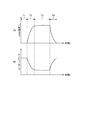
- FIG. 6 is a diagram illustrating an example of a change in the temperature of the wafer W and the power supplied to the heater HT.
- FIG. 6A shows a change in the temperature of the wafer W.
- FIG. 6B shows a change in the power supplied to the heater HT.
- the temperature of the heater HT is controlled to be constant, the plasma is ignited from an unignited state in which the plasma is not ignited, and the temperature of the wafer W and the power supplied to the heater HT are measured.
- An example is shown.
- the temperature of the wafer W was measured using a wafer for temperature measurement such as Etch @ Temp sold by KLA-Tencor.
- the period T1 in FIG. 6 is a non-ignition state in which the plasma is not ignited.
- the power supplied to the heater HT is constant.
- the period T2 in FIG. 6 is an ignition state in which the plasma is ignited, and is a transient state.
- the power supplied to the heater HT decreases.
- the temperature of the wafer W rises to a certain temperature.
- the period T3 in FIG. 6 is an ignition state in which the plasma is ignited.
- the temperature of the wafer W is constant and is in a steady state.
- the period T4 in FIG. 6 is a non-ignition state in which the plasma has been extinguished.
- the temperature of the wafer W decreases, and the power supplied to the heater HT increases.
- the tendency of the power supply to the heater HT to decrease in the transient state shown in the period T2 in FIG. 6 varies depending on the heat input from the plasma to the wafer W, the thermal resistance between the wafer W and the surface of the electrostatic chuck 18, and the like. I do.
- FIG. 7 is a diagram schematically illustrating an example of the flow of energy in the ignition state.
- FIG. 7 is an example of an excessive state.
- a heat of “80” is transmitted from the plasma to the wafer W.
- the heat quantity “60” is transmitted from the wafer W to the surface of the electrostatic chuck 18.
- the heat quantity “40” is transmitted to the heater HT.
- the temperature of the heater HT is controlled to be constant, the heater HT, the amount of heat "60” is generated from the heater power supply HP by the heater power P h.
- the heat of “100” is transmitted from the plasma to the wafer W.
- the heat quantity “80” is transmitted from the wafer W to the surface of the electrostatic chuck 18.
- the heat quantity “60” is transmitted to the heater HT.
- the temperature of the heater HT is controlled to be constant, the heater HT, the amount of heat "40" is generated from the heater power supply HP by the heater power P h.
- a heat of “80” is transmitted from the plasma to the wafer W.
- the heat quantity “40” is transmitted from the wafer W to the surface of the electrostatic chuck 18.
- the heat quantity “20” is transmitted to the heater HT.
- the heater HT For example, if the temperature of the heater HT is controlled to be constant, the heater HT, the amount of heat "80” is generated from the heater power supply HP by the heater power P h.
- the heater power P h is and the amount of heat input from the plasma to the wafer W, heat resistance thus changes between the surface of the wafer W and the electrostatic chuck 18. Therefore, the tendency of the power supplied to the heater HT to decrease during the period T2 shown in FIG. 6B is due to the amount of heat input from the plasma to the wafer W, the thermal resistance between the wafer W and the surface of the electrostatic chuck 18, and the like. Varies by. Therefore, the graph of the power supply to the heater HT in the period T2 can be modeled using the amount of heat input from the plasma to the wafer W and the thermal resistance between the wafer W and the surface of the electrostatic chuck 18 as parameters.
- the change in the power supplied to the heater HT during the period T2 can be modeled by an arithmetic expression using the amount of heat input from the plasma to the wafer W and the thermal resistance between the wafer W and the surface of the electrostatic chuck 18 as parameters.
- the change in the power supplied to the heater HT in the period T2 shown in FIG. 6B is modeled as an expression per unit area.
- the elapsed time from the ignition of the plasma as a t the heater power P h of the elapsed time t and P h (t), when there is a heat flux from the plasma of the elapsed time t of the elapsed time t the heating value q h from the heater HT per unit area of the q h (t).
- the calorific value q h (t) from the heater HT per unit area when there is a heat flux from the plasma at the elapsed time t can be expressed by the following equation (2).
- the calorific value q h_Off from the heater HT per unit area in a steady state when the plasma is not ignited and there is no heat flux from the plasma can be expressed by the following equation (3).
- the thermal resistance R thc ⁇ A per unit area between the surface of the electrostatic chuck 18 and the heater can be expressed by the following equation (4).
- Heat flux q p is the case where the plasma is generated varies if not occurred.
- the heat flux q p_on per unit area from the plasma to the wafer W and the thermal resistance R th ⁇ A per unit area between the wafer W and the surface of the electrostatic chuck 18 are used as parameters, and a 1 , a 2 , a 3 , ⁇ 1 , ⁇ 2 , ⁇ 1 , ⁇ 2 are represented by the following equations (5)-(11), and the heat value q from the heater HT per unit area when there is a heat flux from the plasma.
- h (t) can be expressed as in the following equation (1).
- P h (t) is the heater power [W] when there is a heat flux from the plasma at the elapsed time t.
- Ph_Off is a heater power [W / m 2 ] in a steady state when there is no heat flux from the plasma.
- q h (t) is a calorific value [W / m 2 ] from the heater HT per unit area when there is a heat flux from the plasma at the elapsed time t.
- q h_Off is a calorific value [W / m 2 ] from the heater HT per unit area in a steady state when there is no heat flux from the plasma.
- R th ⁇ A is a heat flux [W / m 2 ] per unit area from the plasma to the wafer W.
- R thc ⁇ A is a thermal resistance [K ⁇ m 2 / W] per unit area between the surface of the electrostatic chuck 18 and the heater.
- A is the area [m 2 ] of the region where the heater is provided.
- ⁇ w is the density [kg / m 3 ] of the wafer W.
- C w is the heat capacity per unit area of the wafer W [J / K ⁇ m 2 ].
- z w is the thickness [m] of the wafer W.
- ⁇ c is the density [kg / m 3 ] of the ceramic constituting the electrostatic chuck 18.
- C c is the heat capacity [J / K ⁇ m 2 ] per unit area of the ceramic constituting the electrostatic chuck 18.
- z c is the distance [m] from the surface of the electrostatic chuck 18 to the heater HT.
- ⁇ c is the thermal conductivity [W / K ⁇ m] of the ceramic constituting the electrostatic chuck 18.
- t is the elapsed time [sec] since the plasma was ignited.
- 1 / a 1 is a time constant indicating the difficulty of warming the wafer W.
- 1 / a 2 is a time constant indicating the difficulty of heat input and the difficulty of warming of the electrostatic chuck 18.
- 1 / a 3 is a time constant that indicates the difficulty of heat penetration of the electrostatic chuck 18 and the difficulty of warming.
- the area A of the heater HT, the density ⁇ w of the wafer W, the heat capacity C w per unit area of the wafer W, the thickness z w of the wafer W, the density ⁇ c of the ceramic constituting the electrostatic chuck 18, and the electrostatic chuck 18 The heat capacity C c per unit area of the constituting ceramic, the distance z c from the surface of the electrostatic chuck 18 to the heater HT, and the heat conduction ⁇ c of the ceramic constituting the electrostatic chuck 18 are the wafer W and the plasma processing apparatus. Each is determined in advance from ten actual configurations.
- R thc ⁇ A is determined in advance by equation (4) from the heat conduction ⁇ c and the distance z c .
- the heater power Ph (t) when there is a heat flux from the plasma for each elapsed time t after the ignition of the plasma, and the heater power Ph_Off in a steady state when there is no heat flux from the plasma It can be obtained by measurement using the plasma processing apparatus 10. Then, as shown in Expressions (2) and (3), each of the obtained heater power Ph (t) and the heater power Ph_Off is divided by the area A of the heater HT, so that the heat flux from the plasma is obtained.
- the calorific value qh (t) per unit area from the heater HT and the calorific value qh_Off from the heater HT per unit area in a steady state when there is no heat flux from the plasma can be determined. it can.
- a graph of the temperature of the wafer W during the period T2 shown in FIG. 6A is also modeled using the amount of heat input from the plasma to the wafer W and the thermal resistance between the wafer W and the surface of the electrostatic chuck 18 as parameters. it can.
- the change in the temperature of the wafer W during the period T2 is modeled as an expression per unit area.
- Equation (12) can be expressed.
- T W (t) is the temperature [° C.] of the wafer W at the elapsed time t.
- T h is the temperature [°C] of the heater HT that is controlled to be constant.
- Temperature T h of the heater HT can be determined from the actual conditions under which the temperature was controlled to a constant wafer W.
- the temperature T W of the wafer W can be calculated from the equation (12). .
- the equation (13) can be determined temperature T h of the heater, the heat flux q P_On, the thermal resistance R th ⁇ A, a temperature T W of the wafer W from R thc ⁇ A.
- the plasma processing apparatus 10 detect the state of the plasma during the plasma processing in order to grasp the status of the plasma processing. For example, in the plasma processing apparatus 10, it is desired to detect a plasma density distribution as a plasma state. In the plasma processing apparatus 10, the amount of heat input from the plasma changes depending on the density distribution of the plasma.
- FIG. 8 is a diagram schematically showing an example of a temperature change between an unignited state and a transient state due to a plasma density distribution.
- FIGS. 8A to 8D show the distribution of the plasma density during the plasma processing and the change in the surface temperature of each divided region of the mounting table 16 in chronological order.
- FIG. 8A shows a non-ignited state. In the unignited state, when plasma is not generated and the power supplied to each heater HT is controlled so that the temperature of each heater HT is constant, the temperature of each divided region of the mounting region 18a is also constant. Become.
- FIGS. 8B to 8D show a transient state. In a region where the plasma density is high, the amount of heat input from the plasma to the mounting region 18a increases.
- the amount of heat input from the plasma to the mounting region 18a is small.
- the center of the mounting area 18a has a heat input amount. More. For this reason, the surface temperature at the center of the mounting area 18a is higher than that near the periphery.
- the power supplied to each heater HT is controlled so that the temperature of each heater HT is constant, the power supplied to the heater HT is reduced in order to reduce the rise in the surface temperature of the mounting area 18a. Since the amount of heat input to the heater HT at the center of the mounting area 18a is large, the power supply is significantly lower than that of the heater HT near the periphery.
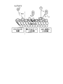
- FIG. 9 is a diagram schematically illustrating an example of the flow of energy in the unignited state and the transient state.
- the placement area 18a is divided into a central portion (Center) near the center of the placement region 18a, a peripheral portion (Middle) surrounding the central portion, and a periphery surrounding the peripheral portion and near the edge of the placement region 18a.
- Center central portion
- Middle peripheral portion
- periphery surrounding the peripheral portion and near the edge of the placement region 18a.
- Edge three zones of an edge portion
- the heat input amount at the center (Center) of the mounting region 18a is "large” and the peripheral portion (Middle).
- the central portion (Center) receives heat of “100” from the plasma and transmits heat of “60” to the heater HT.
- heat of “80” is input from the plasma, and heat of “40” is transmitted to the heater HT.
- heat of “40” is input from the plasma, and heat of “20” is transmitted to the heater HT.
- FIG. 10 is a diagram showing an example of changes in the temperature of the wafer W and the power supplied to the heater HT.
- FIG. 10A shows a change in the temperature of the wafer W in the center portion (Center), the peripheral portion (Middle), and the edge portion (Edge).
- (B) of FIG. 10 illustrates a change in power supply to the heater HT at the center (Center), the periphery (Middle), and the edge (Edge).
- the waveform of the supplied power also changes depending on the amount of heat input.
- the power input to the heater HT in each zone in the unignited state and the transient state is measured, and the heat input amount of each zone is obtained by performing the fitting of the equation (1) using the measurement result for each sone. be able to. Then, the plasma density distribution can be obtained from the heat input amount of each zone. That is, the plasma processing apparatus 10 according to the embodiment can detect the state of the plasma without disposing a sensor in the processing chamber 12.
- the heater control unit 102a controls the temperature of each heater HT.
- the heater control unit 102a outputs control data instructing the power supply to each heater HT to the heater power supply HP, and controls the power supply from the heater power supply HP to each heater HT, thereby controlling each heater HT. Control the temperature of the
- a target set temperature of each heater HT is set in the heater control unit 102a.
- the target temperature of the target wafer W is set as the set temperature of the heater HT in each of the divided regions of the mounting region 18a.
- the target temperature is, for example, a temperature at which the accuracy of the plasma etching on the wafer W is the best.
- the heater control unit 102a controls the power supplied to each heater HT so that each heater HT has a set temperature during the plasma processing. For example, the heater control unit 102a compares, for each divided region, the temperature of each divided region of the mounting region 18a indicated by the temperature data input to the external interface 101, with the set temperature of the divided region. Then, the heater control unit 102a specifies a divided region whose temperature is lower than the set temperature and a divided region whose temperature is higher than the set temperature. The heater control unit 102a outputs, to the heater power supply HP, control data for increasing the supply power to the divided region having a lower temperature than the set temperature and decreasing the supply power for the divided region having a higher temperature than the set temperature.
- the measuring unit 102b measures the power supplied to each heater HT using the power supplied to each heater HT indicated by the power data input to the external interface 101. For example, the measurement unit 102b controls the power supplied to each heater HT by the heater control unit 102a so that the temperature of each heater HT is constant, and supplies the unfired heater HT that does not ignite plasma to the heater HT. Measure the supplied power. In addition, the measurement unit 102b measures the power supplied to each heater HT in a transient state from the time when the plasma is ignited to the time when the fluctuation in the power supplied to each heater HT is stabilized.
- the measurement unit 102b does not ignite the plasma before the start of the plasma processing.
- the power supply to each heater HT in the state is measured.
- the measurement unit 102b measures the power supplied to each heater HT in a transient state from the time when the plasma is ignited to the time when the fluctuation in the power supplied to each heater HT is stabilized.
- the power supplied to each heater HT in the unfired state may be at least one measured by each heater HT, and may be measured a plurality of times and the average value may be used as the power supplied in the unfired state.
- the supply power to each heater HT in the transient state may be measured twice or more.
- the measurement timing for measuring the supplied power is preferably a timing at which the supplied power tends to decrease.
- the measurement timing is preferably separated by a predetermined period or more.
- the measuring unit 102b measures the power supplied to each heater HT at a predetermined cycle (for example, 0.1 second cycle) during the plasma processing. Thereby, a large number of power supplies to each heater HT in the transient state are measured.
- the measuring unit 102b measures the power supplied to each heater HT in the unignited state and the transient state in a predetermined cycle. For example, when the wafer W is replaced and the replaced wafer W is mounted on the mounting table 16 and the plasma processing is performed, the measurement unit 102b supplies the unfired state and the transient state to each heater HT each time. Measure the power. Note that, for example, the parameter calculation unit 102c may measure the power supply to each heater HT in the unignited state and the transient state for each plasma process.
- the parameter calculation unit 102c calculates a heat input amount and a thermal resistance using a calculation model for calculating a supply power in a transient state using the heat input amount from the plasma and the thermal resistance between the wafer W and the heater HT as parameters for each heater HT. I do.
- the parameter calculation unit 102c performs fitting on the calculation model using the supplied power in the unignited state and the transient state measured by the measurement unit 102b, and calculates the heat input amount and the thermal resistance.
- the parameter calculation unit 102c obtains the heater power Ph_Off in the unignited state for each elapsed time t for each heater HT.
- the parameter calculation unit 102c obtains the transient heater power Ph (t) for each elapsed time t for each heater HT.
- the parameter calculation unit 102c divides each of the obtained heater power Ph (t) and the heater power Ph_Off by an area of each heater HT, thereby obtaining a value per unit area of the unignited state for each elapsed time t.
- the calorific value q h_Off from the heater HT and the calorific value q h (t) from the heater HT per unit area in the transient state for each elapsed time t are determined.
- the parameter calculation unit 102c uses the above equations (1) to (11) as a calculation model, and for each heater HT, the calorific value q h (t) from the heater HT per unit area for each elapsed time t, and Then, the heat quantity q h_Off from the heater HT per unit area is fitted to calculate the heat flux q p_on and the heat resistance R th ⁇ A that minimize the error.
- the parameter calculation unit 102c calculates the heat flux q p_on and the thermal resistance R th ⁇ A in a predetermined cycle using the measured supply power in the unignited state and the transient state. For example, each time the wafer W is replaced, the parameter calculation unit 102c uses the supply power of the unignited state and the transient state measured while the wafer W is mounted on the mounting table 16 to determine the heat flux q p_on , And the thermal resistance R th ⁇ A are calculated. Note that, for example, the parameter calculation unit 102c may calculate the heat flux q p_on and the thermal resistance R th ⁇ A using the supplied power in the unignited state and the transient state for each plasma process.
- the output unit 102d controls output of various information.
- the output unit 102d outputs information based on the heat flux q p_on calculated by the parameter calculation unit 102c in a predetermined cycle.
- the output unit 102d outputs information indicating the plasma density distribution to the user interface 103 based on the heat flux q p_on for each heater HT calculated by the parameter calculation unit 102c.
- the output unit 102d outputs to the user interface 103 information indicating the plasma density distribution when the plasma processing is performed on the wafer W.
- the output unit 102d may output information indicating the plasma density distribution to an external device as data.
- FIG. 11A is a diagram illustrating an example of output of information indicating a plasma density distribution.
- the heat flux q p_on of the divided region is displayed in a pattern for each divided region of the mounting region 18a provided with the heater HT.
- FIG. 11B is a diagram illustrating an example of output of information indicating a plasma density distribution.
- the heat flux q p_on of the center part, the peripheral part (Middle), and the edge part (Edge) is shown.
- an abnormality may occur in the state of the plasma in some cases.
- the characteristics of the inside of the processing container 12 may be changed due to the large consumption of the electrostatic chuck 18 or the adhesion of a deposit, and the plasma may be in an abnormal state that is not suitable for the plasma processing. .
- the abnormal wafer W is loaded into the plasma processing apparatus 10.
- the alert unit 102e issues an alert based on the heat input amount calculated in a predetermined cycle by the parameter calculation unit 102c or a change in the heat input amount. For example, the alert unit 102e gives an alert when the heat flux q p_on calculated by the parameter calculating unit 102c in a predetermined cycle is out of a predetermined allowable range. The alert unit 102e gives an alert when the heat flux q p_on calculated by the parameter calculation unit 102c in a predetermined cycle has changed by a predetermined allowable value or more.
- the alert may be of any type as long as an abnormality can be notified to a process manager, a manager of the plasma processing apparatus 10, or the like. For example, the alert unit 102e displays a message that informs the user interface 103 of the abnormality.
- the plasma processing apparatus 10 can notify the occurrence of the abnormality when the characteristics in the processing container 12 or the state of the plasma becomes abnormal due to the loading of the abnormal wafer W or the like.
- the changing unit 102f changes the control parameters of the plasma processing based on the information indicating the plasma density distribution so that the plasma processing on the wafer W is equalized.
- FIG. 12 is a diagram schematically illustrating plasma etching.
- the example of FIG. 12 is a model of a state where the surface of the organic film is plasma-etched with O 2 gas.
- the surface of the organic film is etched by a synergistic effect of adsorption of O radicals, desorption by thermal energy, and desorption by ion collision.
- the etching rate (E / R) of the plasma etching can be expressed by the following equation (14).
- n c is a value indicating the material of the film to be etched.
- ⁇ radical is the supply amount of radical.
- s is the probability of adsorption to the surface.
- K d is the thermal reaction rate.
- ⁇ ion is the amount of incident ions.
- E i is the ion energy.
- k is the reaction probability of ionic desorption.
- the “K d ” part of the equation (14) represents the departure due to thermal energy.
- “KE i ⁇ ⁇ ion ” represents departure due to ion collision.
- the “s ⁇ ⁇ radical ” part indicates the surface adsorption of the radical.
- the plasma concentration distribution affects the desorption due to the ion collision, and the portion of “kE i ⁇ ⁇ ion ” in equation (14) changes depending on the plasma concentration.
- the etching rate also changes depending on the “K d ” portion and the “s ⁇ ⁇ radical ” portion. Therefore, the etching rate can be equalized by changing the “K d ” portion and the “s ⁇ ⁇ radical ” portion according to the plasma density distribution.
- the changing unit 102f controls the plasma processing control parameters affecting the “K d ” part and the “s ⁇ ⁇ radical ” part based on the information indicating the plasma density distribution so that the plasma processing on the wafer W is equalized. To change.
- the portion “K d ” changes depending on the temperature of the wafer W, for example. Further, the portion of “s ⁇ ⁇ radical " changes depending on the concentration of the gas to be turned into plasma.
- the change unit 102f changes the target temperature of the temperature of the wafer W for each divided region of the mounting region 18a based on the information indicating the plasma density distribution. For example, the changing unit 102f changes the target temperature in a divided region having a high plasma density such that departure due to thermal energy is reduced. For example, the changing unit 102f changes the target temperature to be lower. Further, the changing unit 102f changes the target temperature such that departure due to thermal energy increases in a divided region having a low plasma density. For example, the changing unit 102f changes the target temperature to be higher.
- the changing unit 102f performs the division of the upper electrode 30 based on the information indicating the plasma density distribution. Each time, the concentration of the gas to be discharged may be changed. For example, the changing unit 102f changes the gas concentration in the divided region having a high plasma density to be low. The changing unit 102f changes the gas concentration in the divided region having a low plasma density to be high. The changing unit 102f may change the target temperature of the temperature of the wafer W for each divided region and change the concentration of the gas to be discharged for each divided region of the upper electrode 30.
- the set temperature calculation unit 102g calculates, for each heater HT, the set temperature of the heater HT at which the wafer W reaches the target temperature, using the calculated heat input and thermal resistance. For example, the set temperature calculation unit 102g substitutes the calculated heat flux q p_on and the calculated thermal resistance R th ⁇ A for each heater HT into equations (5), (6), and (12). Then, the set temperature calculation unit 102g calculates, for each heater HT, a 1 , a 2 , a 3 , ⁇ 1 , ⁇ 2 , ⁇ 1 , and ⁇ 2 shown in Expressions (5) to (11). (12) the temperature T W from the wafer W to calculate the temperature T h of the heater HT as the target temperature.
- the set temperature calculating section 102g is the elapsed time t as a large predetermined value to the extent that can be regarded as a steady state, calculates the temperature T h of the heater HT to the temperature T W of the wafer W becomes the target temperature.
- Temperature T h of the heater HT to be calculated is the temperature of the heater HT to the temperature of the wafer W becomes the target temperature.
- the temperature T h of the heater HT to the temperature of the wafer W becomes the target temperature may be determined from equation (13).
- the setting temperature calculation unit 102g from equation (12) may calculate the temperature T W of the wafer W at a temperature T h of the following as the current of the heater HT.
- the set temperature calculating section 102g is at a temperature T h of the current of the heater HT, calculates the temperature T W of the wafer W when the elapsed time t was large predetermined value to the extent that can be regarded as a steady state.
- the set temperature calculation unit 102g calculates a difference ⁇ T W between the calculated temperature T W and the target temperature.
- the setting temperature calculation unit 102g has the temperature was subtracted of the difference [Delta] T W from the temperature T h of the current of the heater HT, the temperature of the wafer W may calculate the temperature of the heater HT as the target temperature.
- the set temperature calculation unit 102g corrects the set temperature of each heater HT of the heater control unit 102a to the temperature of the heater HT at which the temperature of the wafer W becomes the target temperature.
- the set temperature calculation unit 102g calculates the temperature of the heater HT at which the temperature of the wafer W reaches the target temperature in a predetermined cycle, and corrects the set temperature of each heater HT. For example, each time the wafer W is replaced, the set temperature calculation unit 102g calculates the temperature of the heater HT at which the temperature of the wafer W becomes the target temperature, and corrects the set temperature of each heater HT. For example, the set temperature calculation unit 102g may calculate the temperature of the heater HT at which the temperature of the wafer W becomes the target temperature and correct the set temperature of each heater HT for each plasma process.
- the plasma processing apparatus 10 can accurately control the temperature of the wafer W during the plasma processing to the target temperature.
- FIG. 13 is a flowchart illustrating an example of a process flow of plasma state detection and plasma state control according to the embodiment. This processing is executed at a predetermined timing, for example, at a timing when the plasma processing is started.
- the heater control unit 102a controls the power supplied to each heater HT so that each heater HT reaches the set temperature (step S10).
- the measuring unit 102b controls the power supply to each heater HT so that the temperature of each heater HT becomes a fixed set temperature by the heater control unit 102a. Is measured (step S11).
- the parameter calculation unit 102c calculates, for each heater HT, the heat generated from the heater HT per unit area obtained by dividing the measured supply power in the non-ignition state and the transient state by the area of the heater HT for the calculation model.
- the amount of heat input and the thermal resistance are calculated by performing fitting using the amount (step S12).
- the parameter calculation unit 102c uses the above equations (1) to (11) as a calculation model, and generates the heat value q h (t) from the heater HT per unit area for each elapsed time t for each heater HT.
- the heat value q h_Off from the heater HT per unit area is fitted to calculate the heat flux q p_on and the heat resistance R th ⁇ A that minimize the error.
- the output unit 102d outputs information based on the heat input amount calculated by the parameter calculation unit 102c (Step S13). For example, the output unit 102d outputs information indicating the plasma density distribution to the user interface 103 based on the heat flux q p_on for each heater HT calculated by the parameter calculation unit 102c.
- the changing unit 102f changes the control parameters of the plasma processing based on the information indicating the plasma density distribution so that the plasma processing on the wafer W is equalized (step S14). For example, the changing unit 102f changes the target temperature of the temperature of the wafer W for each divided region of the mounting region 18a based on the information indicating the plasma density distribution.
- the set temperature calculation unit 102g calculates, for each heater HT, the set temperature of the heater HT at which the wafer W reaches the target temperature using the calculated heat input amount and thermal resistance (step S15). For example, the set temperature calculation unit 102g substitutes the calculated heat flux q p_on and the calculated thermal resistance R th ⁇ A for each heater HT into equations (5), (6), and (12). Then, the set temperature calculation unit 102g calculates the wafer from equation (12) using a 1 , a 2 , a 3 , ⁇ 1 , ⁇ 2 , ⁇ 1 , and ⁇ 2 shown in equations (5) to (11). temperature T W of W to calculate the temperature T h of the heater HT as a target temperature. The temperature T h of the heater HT to the temperature of the wafer W becomes the target temperature may be determined from equation (13).
- the set temperature calculation unit 102g corrects the set temperature of each heater HT of the heater control unit 102a to the set temperature of the heater HT at which the temperature of the wafer W becomes the target temperature (step S16), and ends the process.
- the plasma processing apparatus 10 includes the mounting table 16, the heater control unit 102a, the measurement unit 102b, the parameter calculation unit 102c, and the output unit 102d.
- the mounting table 16 is provided with a heater HT capable of adjusting the temperature of the mounting surface on which the wafer W is mounted.
- the heater control unit 102a controls power supplied to the heater HT so that the heater HT has a set temperature.
- the measuring unit 102b controls the electric power supplied to the heater HT by the heater control unit 102a so that the temperature of the heater HT becomes constant, and a non-ignited state in which the plasma is not ignited and a heater HT after the plasma is ignited.
- the parameter calculation unit 102c includes the amount of heat input from the plasma as a parameter, and performs fitting using a supply model in the unignited state and the transition state measured by the measurement unit 102b with respect to a calculation model for calculating the supply state in the transition state. To calculate the heat input.
- the output unit 102d outputs information based on the heat input amount calculated by the parameter calculation unit 102c. Thereby, the plasma processing apparatus 10 can detect the state of plasma without disposing a sensor in the processing chamber 12.
- the heater HT is individually provided for each of the divided regions of the mounting surface of the mounting table 16.
- the heater control unit 102a controls the power supply for each heater HT so that the heater HT provided for each region has a set temperature set for each region.
- the measurement unit 102b controls the supply power so that the temperature is constant for each heater HT by the heater control unit 102a, and measures the supply power in the non-ignition state and the transition state for each heater HT.
- the parameter calculation unit 102c performs fitting using the supply power in the non-ignition state and the transient state measured by the measurement unit 102b on the calculation model for each heater HT, and calculates the heat input amount for each heater HT. .
- the output unit 102d outputs information indicating the plasma density distribution based on the heat input amount for each heater HT calculated by the parameter calculation unit 102c.
- the plasma processing apparatus 10 can provide information indicating the plasma density distribution during the plasma processing without disposing a sensor in the processing chamber 12.
- the plasma processing apparatus 10 further includes a changing unit 102f.
- the changing unit 102f changes the control parameters of the plasma processing based on the plasma density distribution so that the plasma processing on the wafer W is equalized. Thereby, the plasma processing apparatus 10 can equalize the plasma processing on the wafer W.
- the plasma processing apparatus 10 further includes an alert unit 102e.
- the alert unit 102e issues an alert based on the information output by the output unit 102d or a change in the information.
- the plasma processing apparatus 10 can perform an alert when an abnormality occurs in the state of the plasma.
- the case where the plasma processing is performed on the semiconductor wafer as the object to be processed has been described as an example.
- the object may be any object as long as the temperature affects the progress of the plasma processing.
- the object to be processed may be a glass substrate or the like.
- the plasma processing may be any processing using plasma.
- the plasma treatment chemical vapor deposition (CVD), atomic layer deposition (ALD), ashing, plasma doping, plasma annealing, and the like can be given.
- the plasma processing apparatus 10 has the base 20 connected to the first high-frequency power supply HFS for plasma generation and the second high-frequency power supply LFS for bias power, but is not limited to this.
- the first high-frequency power supply HFS for plasma generation may be connected to the upper electrode 30 via the matching unit MU.
- the plasma processing apparatus 10 is a capacitively coupled parallel plate plasma processing apparatus.
- the plasma processing apparatus 10 can be applied to any plasma processing apparatus.
- the plasma processing apparatus 10 may be any type of plasma processing apparatus such as an inductively coupled plasma processing apparatus or a plasma processing apparatus that excites a gas with a surface wave such as a microwave.
- the changing unit 102f changes the target temperature of the wafer W for each divided region of the mounting region 18a based on the information indicating the plasma density distribution
- the changing unit 102f outputs the information indicating the plasma density distribution.
- the plasma density may be changed for each division of the plasma generation. Note that, for example, in the case of a capacitively coupled parallel plate plasma processing apparatus, the upper electrode 30 is divided for each divided region and the upper electrode 30 is divided for each divided upper electrode.
- the case where the heater HT is provided in each of the divided areas obtained by dividing the mounting area 18a of the mounting table 16 has been described as an example, but the invention is not limited to this.
- One heater HT is provided on the entire mounting area 18a of the mounting table 16, the power supplied to the heater HT in the unignited state and the transient state is measured, and the measurement result is fitted to the calculation model, The heat input may be calculated. Since the calculated heat input is the heat input of the entire plasma, the state of the entire plasma can be detected from the calculated heat input.
- FIG. 14 is a plan view illustrating an example of division of the mounting surface of the mounting table according to the embodiment.
- the mounting area 18a of the mounting table 16 may be divided into a lattice shape, and a heater HT may be provided in each of the divided areas.
- the amount of heat input can be detected for each of the grid-shaped divided regions, and the plasma density distribution can be obtained in more detail.
- Reference Signs List 10 plasma processing device 16 mounting table 18 electrostatic chuck 18a mounting area 20 base 100 control unit 102 process controller 102a heater control unit 102b measurement unit 102c parameter calculation unit 102d output unit 102e alert unit 102f change unit 102g set temperature calculation unit HP Heater power supply HT Heater PD Power detector TD Temperature measuring device W Wafer
Landscapes
- Engineering & Computer Science (AREA)
- Physics & Mathematics (AREA)
- Plasma & Fusion (AREA)
- Chemical & Material Sciences (AREA)
- Analytical Chemistry (AREA)
- General Physics & Mathematics (AREA)
- Automation & Control Theory (AREA)
- Manufacturing & Machinery (AREA)
- Emergency Management (AREA)
- Business, Economics & Management (AREA)
- Remote Sensing (AREA)
- Spectroscopy & Molecular Physics (AREA)
- Drying Of Semiconductors (AREA)
- Chemical Vapour Deposition (AREA)
- Plasma Technology (AREA)
- Container, Conveyance, Adherence, Positioning, Of Wafer (AREA)
Priority Applications (6)
| Application Number | Priority Date | Filing Date | Title |
|---|---|---|---|
| US16/978,134 US11935731B2 (en) | 2018-06-29 | 2019-06-17 | Plasma processing apparatus, plasma state detection method, and plasma state detection program |
| CN201980013656.8A CN111801990B (zh) | 2018-06-29 | 2019-06-17 | 等离子体处理装置、等离子体状态检测方法以及等离子体状态检测程序 |
| KR1020247025479A KR20240122911A (ko) | 2018-06-29 | 2019-06-17 | 플라스마 처리 장치, 플라스마 상태 검출 방법 및 플라스마 상태 검출 프로그램 |
| CN202311155125.7A CN117238742A (zh) | 2018-06-29 | 2019-06-17 | 等离子体处理装置、等离子体状态检测方法以及程序 |
| KR1020207025491A KR102690560B1 (ko) | 2018-06-29 | 2019-06-17 | 플라스마 처리 장치, 플라스마 상태 검출 방법 및 플라스마 상태 검출 프로그램 |
| US18/442,022 US20240186125A1 (en) | 2018-06-29 | 2024-02-14 | Plasma processing apparatus, plasma state detection method, and plasma state detection program |
Applications Claiming Priority (6)
| Application Number | Priority Date | Filing Date | Title |
|---|---|---|---|
| JP2018124896 | 2018-06-29 | ||
| JP2018-124896 | 2018-06-29 | ||
| JP2019032013 | 2019-02-25 | ||
| JP2019-032013 | 2019-02-25 | ||
| JP2019-099609 | 2019-05-28 | ||
| JP2019099609A JP7202972B2 (ja) | 2018-06-29 | 2019-05-28 | プラズマ処理装置、プラズマ状態検出方法およびプラズマ状態検出プログラム |
Related Child Applications (2)
| Application Number | Title | Priority Date | Filing Date |
|---|---|---|---|
| US16/978,134 A-371-Of-International US11935731B2 (en) | 2018-06-29 | 2019-06-17 | Plasma processing apparatus, plasma state detection method, and plasma state detection program |
| US18/442,022 Continuation US20240186125A1 (en) | 2018-06-29 | 2024-02-14 | Plasma processing apparatus, plasma state detection method, and plasma state detection program |
Publications (1)
| Publication Number | Publication Date |
|---|---|
| WO2020004091A1 true WO2020004091A1 (ja) | 2020-01-02 |
Family
ID=68985637
Family Applications (1)
| Application Number | Title | Priority Date | Filing Date |
|---|---|---|---|
| PCT/JP2019/023793 Ceased WO2020004091A1 (ja) | 2018-06-29 | 2019-06-17 | プラズマ処理装置、プラズマ状態検出方法およびプラズマ状態検出プログラム |
Country Status (6)
| Country | Link |
|---|---|
| US (1) | US20240186125A1 (https=) |
| JP (1) | JP7527342B2 (https=) |
| KR (1) | KR20240122911A (https=) |
| CN (1) | CN117238742A (https=) |
| TW (2) | TWI819012B (https=) |
| WO (1) | WO2020004091A1 (https=) |
Cited By (1)
| Publication number | Priority date | Publication date | Assignee | Title |
|---|---|---|---|---|
| CN113889392A (zh) * | 2020-07-02 | 2022-01-04 | 东京毅力科创株式会社 | 等离子体处理装置 |
Citations (6)
| Publication number | Priority date | Publication date | Assignee | Title |
|---|---|---|---|---|
| JP2002009064A (ja) * | 2000-06-21 | 2002-01-11 | Hitachi Ltd | 試料の処理装置及び試料の処理方法 |
| JP2004247526A (ja) * | 2003-02-14 | 2004-09-02 | Hitachi High-Technologies Corp | プラズマ処理装置及び方法 |
| JP2010199107A (ja) * | 2009-02-23 | 2010-09-09 | Mitsubishi Heavy Ind Ltd | プラズマ処理装置の基板支持台 |
| JP2015092580A (ja) * | 2014-11-28 | 2015-05-14 | 株式会社日立ハイテクノロジーズ | 試料の温度を制御する温度制御装置、試料を載置する試料台及びこれらを備えたプラズマ処理装置 |
| JP2017005128A (ja) * | 2015-06-11 | 2017-01-05 | 東京エレクトロン株式会社 | 温度制御方法及びプラズマ処理装置 |
| JP2019091880A (ja) * | 2017-11-16 | 2019-06-13 | 東京エレクトロン株式会社 | プラズマ処理装置、温度制御方法および温度制御プログラム |
Family Cites Families (20)
| Publication number | Priority date | Publication date | Assignee | Title |
|---|---|---|---|---|
| JP2003197609A (ja) * | 2001-12-27 | 2003-07-11 | Tokyo Electron Ltd | プラズマ処理装置の監視方法及びプラズマ処理装置 |
| JP5183058B2 (ja) * | 2006-07-20 | 2013-04-17 | アプライド マテリアルズ インコーポレイテッド | 急速温度勾配コントロールによる基板処理 |
| JP5203612B2 (ja) * | 2007-01-17 | 2013-06-05 | 株式会社日立ハイテクノロジーズ | プラズマ処理装置 |
| KR100978886B1 (ko) * | 2007-02-13 | 2010-08-31 | 가부시키가이샤 히다치 하이테크놀로지즈 | 플라즈마처리방법 및 플라즈마처리장치 |
| JP2009087790A (ja) | 2007-09-29 | 2009-04-23 | Tokyo Electron Ltd | 電子密度測定装置及び電子密度測定方法並びに記憶媒体 |
| JP2009194032A (ja) | 2008-02-12 | 2009-08-27 | Tokyo Electron Ltd | プラズマ測定方法及びプラズマ測定装置並びに記憶媒体 |
| JP5433171B2 (ja) * | 2008-06-16 | 2014-03-05 | 株式会社日立ハイテクノロジーズ | 試料温度の制御方法 |
| JP5059792B2 (ja) * | 2009-01-26 | 2012-10-31 | 東京エレクトロン株式会社 | プラズマ処理装置 |
| KR101644673B1 (ko) * | 2009-12-15 | 2016-08-01 | 램 리써치 코포레이션 | Cd 균일성을 향상시키기 위한 기판 온도의 조절 |
| JP6023787B2 (ja) | 2011-03-28 | 2016-11-09 | 東京エレクトロン株式会社 | イオンエネルギーアナライザ、イオンエネルギーアナライザを有する診断用ウエハ |
| US9263240B2 (en) * | 2011-11-22 | 2016-02-16 | Lam Research Corporation | Dual zone temperature control of upper electrodes |
| US10049948B2 (en) * | 2012-11-30 | 2018-08-14 | Lam Research Corporation | Power switching system for ESC with array of thermal control elements |
| JP6030994B2 (ja) * | 2013-05-15 | 2016-11-24 | 東京エレクトロン株式会社 | プラズマエッチング装置及びプラズマエッチング方法 |
| JP6180924B2 (ja) * | 2013-12-26 | 2017-08-16 | 東京エレクトロン株式会社 | 熱流束測定方法、基板処理システム及び熱流束測定用部材 |
| US10141166B2 (en) * | 2014-08-15 | 2018-11-27 | Applied Materials, Inc. | Method of real time in-situ chamber condition monitoring using sensors and RF communication |
| JP6361495B2 (ja) * | 2014-12-22 | 2018-07-25 | 東京エレクトロン株式会社 | 熱処理装置 |
| JP6452449B2 (ja) * | 2015-01-06 | 2019-01-16 | 東京エレクトロン株式会社 | 載置台及び基板処理装置 |
| JP6570894B2 (ja) * | 2015-06-24 | 2019-09-04 | 東京エレクトロン株式会社 | 温度制御方法 |
| US10522377B2 (en) * | 2016-07-01 | 2019-12-31 | Lam Research Corporation | System and method for substrate support feed-forward temperature control based on RF power |
| US11236422B2 (en) * | 2017-11-17 | 2022-02-01 | Lam Research Corporation | Multi zone substrate support for ALD film property correction and tunability |
-
2019
- 2019-06-17 WO PCT/JP2019/023793 patent/WO2020004091A1/ja not_active Ceased
- 2019-06-17 CN CN202311155125.7A patent/CN117238742A/zh active Pending
- 2019-06-17 KR KR1020247025479A patent/KR20240122911A/ko active Pending
- 2019-06-27 TW TW108122530A patent/TWI819012B/zh active
- 2019-06-27 TW TW112135383A patent/TWI882440B/zh active
-
2022
- 2022-12-26 JP JP2022207737A patent/JP7527342B2/ja active Active
-
2024
- 2024-02-14 US US18/442,022 patent/US20240186125A1/en active Pending
Patent Citations (6)
| Publication number | Priority date | Publication date | Assignee | Title |
|---|---|---|---|---|
| JP2002009064A (ja) * | 2000-06-21 | 2002-01-11 | Hitachi Ltd | 試料の処理装置及び試料の処理方法 |
| JP2004247526A (ja) * | 2003-02-14 | 2004-09-02 | Hitachi High-Technologies Corp | プラズマ処理装置及び方法 |
| JP2010199107A (ja) * | 2009-02-23 | 2010-09-09 | Mitsubishi Heavy Ind Ltd | プラズマ処理装置の基板支持台 |
| JP2015092580A (ja) * | 2014-11-28 | 2015-05-14 | 株式会社日立ハイテクノロジーズ | 試料の温度を制御する温度制御装置、試料を載置する試料台及びこれらを備えたプラズマ処理装置 |
| JP2017005128A (ja) * | 2015-06-11 | 2017-01-05 | 東京エレクトロン株式会社 | 温度制御方法及びプラズマ処理装置 |
| JP2019091880A (ja) * | 2017-11-16 | 2019-06-13 | 東京エレクトロン株式会社 | プラズマ処理装置、温度制御方法および温度制御プログラム |
Cited By (1)
| Publication number | Priority date | Publication date | Assignee | Title |
|---|---|---|---|---|
| CN113889392A (zh) * | 2020-07-02 | 2022-01-04 | 东京毅力科创株式会社 | 等离子体处理装置 |
Also Published As
| Publication number | Publication date |
|---|---|
| TWI882440B (zh) | 2025-05-01 |
| CN117238742A (zh) | 2023-12-15 |
| TW202418346A (zh) | 2024-05-01 |
| TWI819012B (zh) | 2023-10-21 |
| KR20240122911A (ko) | 2024-08-13 |
| JP7527342B2 (ja) | 2024-08-02 |
| JP2023033331A (ja) | 2023-03-10 |
| TW202015094A (zh) | 2020-04-16 |
| US20240186125A1 (en) | 2024-06-06 |
Similar Documents
| Publication | Publication Date | Title |
|---|---|---|
| CN111933508B (zh) | 等离子体处理装置、温度控制方法以及记录介质 | |
| JP7313509B2 (ja) | プラズマ処理装置、温度制御方法および温度制御プログラム | |
| JP7068971B2 (ja) | プラズマ処理装置、温度制御方法および温度制御プログラム | |
| JP7202972B2 (ja) | プラズマ処理装置、プラズマ状態検出方法およびプラズマ状態検出プログラム | |
| JP2023099617A (ja) | プラズマ処理装置、監視方法および監視プログラム | |
| TW202029258A (zh) | 電漿處理裝置、計算方法及計算程式 | |
| JP7214562B2 (ja) | プラズマ処理装置、算出方法および算出プログラム | |
| JP7527342B2 (ja) | プラズマ処理装置、プラズマ状態検出方法およびプラズマ状態検出プログラム |
Legal Events
| Date | Code | Title | Description |
|---|---|---|---|
| 121 | Ep: the epo has been informed by wipo that ep was designated in this application |
Ref document number: 19824789 Country of ref document: EP Kind code of ref document: A1 |
|
| NENP | Non-entry into the national phase |
Ref country code: DE |
|
| 122 | Ep: pct application non-entry in european phase |
Ref document number: 19824789 Country of ref document: EP Kind code of ref document: A1 |