WO2020003359A1 - 光学式マーク読取装置及びこれを備えた電子機器製造装置 - Google Patents
光学式マーク読取装置及びこれを備えた電子機器製造装置 Download PDFInfo
- Publication number
- WO2020003359A1 WO2020003359A1 PCT/JP2018/024058 JP2018024058W WO2020003359A1 WO 2020003359 A1 WO2020003359 A1 WO 2020003359A1 JP 2018024058 W JP2018024058 W JP 2018024058W WO 2020003359 A1 WO2020003359 A1 WO 2020003359A1
- Authority
- WO
- WIPO (PCT)
- Prior art keywords
- mark
- reading
- imaging
- angle
- imaging device
- Prior art date
- Legal status (The legal status is an assumption and is not a legal conclusion. Google has not performed a legal analysis and makes no representation as to the accuracy of the status listed.)
- Ceased
Links
Images


Classifications
-
- G—PHYSICS
- G06—COMPUTING OR CALCULATING; COUNTING
- G06K—GRAPHICAL DATA READING; PRESENTATION OF DATA; RECORD CARRIERS; HANDLING RECORD CARRIERS
- G06K7/00—Methods or arrangements for sensing record carriers, e.g. for reading patterns
- G06K7/10—Methods or arrangements for sensing record carriers, e.g. for reading patterns by electromagnetic radiation, e.g. optical sensing; by corpuscular radiation
-
- H—ELECTRICITY
- H05—ELECTRIC TECHNIQUES NOT OTHERWISE PROVIDED FOR
- H05K—PRINTED CIRCUITS; CASINGS OR CONSTRUCTIONAL DETAILS OF ELECTRIC APPARATUS; MANUFACTURE OF ASSEMBLAGES OF ELECTRICAL COMPONENTS
- H05K13/00—Apparatus or processes specially adapted for manufacturing or adjusting assemblages of electric components
- H05K13/08—Monitoring manufacture of assemblages
Definitions
- the technology disclosed in this specification relates to an optical mark reading device and an electronic device manufacturing apparatus including the same.
- components that make up an electronic device may be marked with an optically readable mark for traceability.
- the mark attached to the component is read at a manufacturing facility that manufactures electronic devices.
- a reading device is used for capturing the image of the mark and recognizing information held in the mark from the captured image.
- Patent Document 1 Japanese Patent Application Laid-Open No. 2005-165802 discloses an example of an optical mark reading device.
- the optical mark reading device of Patent Document 1 is configured to be able to move the position of the imaging unit provided in the imaging device.
- the focal length of the imaging device is adjusted by moving the position of the imaging unit.
- the accuracy of reading the mark is improved by adjusting the focal length.
- the imaging angle formed by the mark installation surface with the mark and the optical axis of the imaging device does not change. Therefore, for example, when the mark printing state is poor and the mark is distorted, it may be difficult to improve the mark reading accuracy only by adjusting the focal length.
- the present specification provides a new and useful technique capable of improving the reading accuracy of an optical mark.
- the optical mark reading device includes an imaging device that captures a mark, a reading unit that performs a reading process that reads information from an image captured by the imaging device, and a position adjustment device that adjusts the position of the imaging device with respect to the mark. And a control unit for controlling the position adjusting device.
- the position adjustment device is configured to be able to adjust an angle between the mark installation surface and the optical axis of the imaging device.
- the control unit is configured to be able to execute a positioning process of positioning the photographing device at a preset position with respect to the mark by driving the position adjusting device. Further, the control unit is configured to, when the reading unit fails to read the mark from the image captured by the imaging device positioned at the set position, use the position adjustment device to determine an imaging angle between the mark installation surface and the optical axis of the imaging device. It is configured to be able to execute an angle adjustment process for adjusting.
- the optical mark reading device includes a position adjusting device configured to be able to adjust an imaging angle formed between the mark installation surface and the optical axis of the imaging device. Therefore, the position adjustment device can adjust the imaging angle between the mark installation surface and the optical axis of the imaging device. Therefore, for example, even when the mark provided on the mark installation surface is distorted, the reading probability of the mark can be improved by adjusting the imaging angle.
- FIG. 1 is a schematic diagram illustrating a configuration of an electronic device manufacturing apparatus 100 according to an embodiment.
- FIG. 2 is a schematic diagram showing a positional relationship between the optical mark reader and the substrate when the optical mark reader reads a mark provided on a substrate.
- 5 is a flowchart showing a procedure for reading an optical mark.
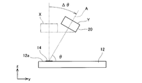
- FIG. 4 is a diagram illustrating an angle adjustment process of the optical mark reading device 10.
- the control unit when performing the angle adjustment process, may adjust the imaging angle to a preset angle irrespective of the state of the image for which the reading of the mark has failed. . According to such a configuration, it is only necessary to adjust the imaging angle to a preset angle, so that it is not necessary to analyze an image for which mark reading has failed, and the configuration of the control unit can be simplified. When the reading of the mark fails, the reading of the mark is often successful by finely adjusting the imaging angle within a predetermined angle range. Therefore, even if the image in which the reading of the mark has failed is not analyzed, the reading probability of the mark does not change significantly.
- the imaging device may capture the mark at predetermined time intervals while the imaging angle is being adjusted by the angle adjustment processing.
- the reading unit may execute a reading process on each of the images captured by the imaging device at predetermined time intervals.
- the control unit may end the angle adjustment processing when the reading unit succeeds in reading the mark during the execution of the angle adjustment processing. According to such a configuration, the imaging and reading processing of the mark is performed while adjusting the imaging angle until the reading of the mark is successful.
- the optical mark reading device when the mark is successfully read, stores relative position data that defines a relative position and an imaging angle between the component and the imaging device when the reading is successful.
- a storage unit may be further provided.
- the control unit may adjust the imaging angle based on the relative position data stored in the storage unit in the angle adjustment processing. If the attributes related to the manufacturing history of the marked parts (for example, manufacturing lots and manufacturing lines) are of the same type, the states of the marks attached to the parts (for example, the characteristics of how the marks are distorted) should be similar. There are many. Therefore, by performing the angle adjustment processing based on the relative position data when the mark has been successfully read, the time required for reading the mark can be reduced.
- a data analysis unit that derives the reading probability of the mark of the relative position data from the statistical result of the relative position data in the storage unit may be further provided.
- the control unit may adjust the imaging angle in descending order of the reading probability of the relative position data. As a result, the time required for reading the mark can be further reduced.
- the position adjustment device may include a lens that can be arranged on the optical axis of the imaging device, and an actuator that adjusts the position of the lens with respect to the optical axis of the imaging device.
- the imaging angle may be adjusted by the actuator adjusting the position of the lens. Since only the position of the lens is adjusted by the actuator, the movable portion can be made smaller, and the device can be made smaller.
- the position adjustment device may be an articulated robot.
- the position adjusting device may adjust the image capturing angle by adjusting the attitude of the image capturing device with respect to the mark installation surface.
- the mark may be a two-dimensional code.
- an electronic device manufacturing apparatus reads an assembling device that assembles components that constitute an electronic device and an optical mark that is attached to a mark installation surface of the components that constitute the electronic device. And the above-mentioned optical mark reader.
- the electronic device manufacturing apparatus 100 is a component mounter that is installed on a manufacturing line for manufacturing a substrate 12 (an example of an electronic device) provided with electronic components and mounts the electronic components on the substrate 12. As shown in FIG. 2, a plurality of electronic components are mounted on the substrate 12. A mark installation surface 12a is provided at a predetermined position on the upper surface (xy plane) of the substrate 12, and an optical mark 14 is provided on the mark installation surface 12a.
- the mark 14 is a matrix type two-dimensional code, and holds information (for example, a serial number) for specifying the substrate 12.
- the electronic device manufacturing apparatus 100 specifies the substrate 12 and stores the work performed on the substrate 12.
- a two-dimensional code such as a QR code (registered trademark) or a data matrix can be adopted.
- the electronic device manufacturing apparatus 100 includes an assembling apparatus 50 and a transport apparatus 60.
- the assembly device 50 mounts components supplied from the component supply feeder at predetermined positions on the board 12.
- the assembling apparatus 50 includes, for example, a head provided with nozzles and an xy robot mechanism that drives the head in the xy directions.
- the components supplied from the component feeder are sucked by the nozzles, and the head is positioned at a predetermined position with respect to the substrate 12, whereby the components sucked by the nozzles are mounted on the substrate 12.
- the transfer device 60 carries the substrate 12 into and out of the electronic device manufacturing apparatus 100.
- the transport device 60 When the transport device 60 carries the substrate 12 to the component mounting position in the electronic device manufacturing apparatus 100, the components are mounted on the substrate 12 by the assembling device 50, and the mark 14 by the optical mark reading device 10 described later is used. Is read.
- the transport device 60 includes, for example, a pair of belt conveyors 62, a supporting device (not shown) attached to the belt conveyor 62 and supporting the substrate 12 from below, and a driving device (not shown) for driving the belt conveyor 62. be able to.
- the electronic device manufacturing apparatus 100 includes the optical mark reading device 10.
- the optical mark reading device 10 includes an imaging device 20, a position adjustment device 30, and a control device 40.
- the image capturing device 20 is a device that captures an image of the mark 14, and may use the image capturing device 20 provided in a known two-dimensional code reader.
- the imaging device 20 can be configured by, for example, an illuminator that illuminates the mark 14, a camera that captures the mark 14, and a lens that is arranged between the camera and the mark 14.
- the imaging device 20 is attached to a tip of a support shaft 34 (shown in FIG. 2), and is arranged so as to be able to image the mark 14 attached to the mark installation surface 12 a of the substrate 12 from above the substrate 12.
- the position adjustment device 30 is a device that adjusts the position of the imaging device 20 with respect to the mark 14.
- the position adjustment device 30 includes an xy movement mechanism that moves the imaging device 20 in the xy directions (see FIG. 2). By driving the xy movement mechanism of the position adjustment device 30, the imaging device 20 can be moved to a predetermined position with respect to the mark 14. In the position adjustment by the xy movement mechanism of the position adjustment device 30, the imaging device 20 moves parallel to the mark installation surface 12a.
- the position adjusting device 30 further rotates the imaging device 20 around the axis (x-axis a1) of the support shaft 34, and the imaging device 20 around the y-axis a2.
- a second rotation mechanism is provided.
- the imaging device 20 rotates around the x-axis a1, and the imaging angle ⁇ between the mark installation surface 12a and the optical axis A of the imaging device 20 is adjusted. That is, as shown in FIG. 4, the imaging device 20 rotates in the yz plane, and the imaging angle ⁇ with respect to the mark installation surface 12a changes. Therefore, by driving the xy movement mechanism and the first rotation mechanism, the mark 14 can be imaged by the imaging device 20 (the state shown in FIG. 4).
- the imaging device 20 is rotated around the x axis (a1 in FIG. The distortion can be corrected.
- the imaging device 20 rotates around the y-axis (a2 in FIG. 2), the imaging device 20 rotates in the xz plane, and the mark is set.
- the imaging angle ⁇ with respect to the surface 12a changes. Therefore, for example, when the mark 14 is distorted in the x direction and the lengths of both sides of the mark 14 extending in the y direction are different, the image pickup device 20 is rotated around the y axis (a2 in FIG. Fourteen distortions can be corrected.
- a mobile robot having a plurality of degrees of freedom is used for the position adjustment device 30.
- the driving of the xy movement mechanism, the first rotation mechanism, and the second rotation mechanism of the position adjustment device 30 is controlled by the control device 40. That is, the position adjustment device 30 and the control device 40 are connected by the cable 32 (shown in FIG. 2), and the position adjustment device 30 is controlled by a control signal transmitted from the control device 40.
- Control device 40 is a CPU. ROM. It is constituted by a computer having a RAM.
- the control device 40 includes a control unit 42, a reading unit 44, and a storage unit 46, and various functions are provided by executing a program installed in advance.
- the position adjusting device 30 is driven to position the mark 14 at a predetermined position (imaging angle) with respect to the mark 14, and the position adjusting device 30 is driven to move the mark installation surface 12 a and the imaging device 20. It functions as the control unit 42 that adjusts the imaging angle with the optical axis A.
- the control device 40 functions as a reading unit 44 that executes a reading process of reading information from an image captured by the imaging device 20.
- the control device 40 functions as a storage unit 46 that stores the relative position data defining the relative position and the imaging angle between the substrate 12 and the imaging device 20 when the reading is successful.
- step S12 a positioning process of the imaging device 20 with respect to the mark 14 is performed.
- the control unit 42 of the control device 40 drives the xy movement mechanism of the position adjustment device 30 to position the imaging device 20 at a predetermined imaging position X. That is, the mark 14 is attached to a predetermined position on the upper surface of the substrate 12 and is known, and the position where the substrate 12 is positioned in the electronic device manufacturing apparatus 100 (that is, the component mounting position) is also known. . Therefore, the control device 40 positions the imaging device 20 such that the imaging device 20 faces the mark 14 provided on the substrate 12.
- the position information of the imaging position X at which the imaging device 20 is positioned is stored in the storage unit 46 of the control device 40.
- step S14 the control device 40 captures an image of the mark 14 using the imaging device 20.
- step S16 the control device 40 executes a process of reading information from the image of the mark 14 imaged in step S14.
- the reading process in step S16 can be a reading process executed by a known two-dimensional code reader.
- step S18 the control device 40 determines whether the reading process by the reading unit 44 has been successful. That is, when the imaging device 20 is positioned with respect to the mark 14 in step S12, the imaging angle ⁇ formed by the mark installation surface 12a and the optical axis A of the imaging device 20 is orthogonal. For this reason, when the printing state of the mark 14 is good, the reading of the mark 14 succeeds, but the printing state of the mark 14 is poor, for example, when the mark 14 attached to the mark installation surface 12a is distorted. In some cases, the mark 14 cannot be read. For this reason, in the present embodiment, it is determined whether the reading of the mark 14 has been successful in step S18. If the reading unit 44 has failed in reading, the process proceeds to step S20. If the reading unit 44 has succeeded in reading, the process proceeds to step S22.
- step S20 the control unit 42 of the control device 40 executes an angle adjustment process of the imaging device 20.
- the control unit 42 drives the xy movement mechanism and the first rotation mechanism of the position adjustment device 30 and sets a predetermined imaging position X (an imaging position that was previously imaged) from a predetermined imaging position X.
- the position of the imaging device 20 is adjusted to the imaging position Y (the adjusted imaging position). Accordingly, the imaging angle ⁇ between the mark installation surface 12a of the substrate 12 and the optical axis A of the imaging device 20 changes by ⁇ .
- the imaging position Y for positioning the imaging device 20 is stored in the storage unit 46 of the control device 40 in advance.
- step S20 is executed irrespective of the state of the image for which the reading of the mark 14 has failed. That is, the image capturing apparatus 20 is moved to the predetermined image capturing position Y without performing processing such as analyzing the image in which the reading of the mark 14 has failed and identifying the cause of the failure. Therefore, there is no need to provide a program for analyzing the captured image, and it is not necessary to improve the performance of the mark 14 reading program.
- step S14 When the imaging device 20 is positioned at the predetermined imaging position Y in step S20, the process moves to step S14, and these steps are repeatedly executed until steps S16 and S18 and reading of the mark 14 succeed. Accordingly, the imaging device 20 captures the mark 14 while changing the capturing angle ⁇ , and performs a reading process on the captured image. When the reading of the mark 14 fails, the reading of the mark 14 is often successful by finely adjusting the imaging angle ⁇ . Therefore, the mark 14 can be read successfully by repeating the steps S14 to S20.
- step S22 the relative position data between the substrate 12 (the mark setting surface 12a) and the imaging device 20 is stored in the storage unit 46 of the control device 40.
- the control device 40 changes the position of the imaging device 20 (the position of the xy movement mechanism, the first rotation mechanism, and the second rotation mechanism) when the reading of the mark 14 is successful, with respect to the substrate 12.
- the data is stored in the storage unit 46 as relative position data. Note that the position data stored in the storage unit 46 can be used as the predetermined imaging position X in step S12 when reading the mark 14 attached to the substrate 12 to be subsequently manufactured.
- the processing from step S14 is performed after the angle adjustment processing of the imaging device 20 is performed in step S20.
- the present invention is not limited to this.
- the processing of steps S16 and S18 may be performed during the execution of.
- the reading unit 44 succeeds in reading the mark 14
- the angle adjustment process that is being performed may be ended. That is, even while the imaging device 20 is moving toward the predetermined imaging position Y based on the trajectory data, the imaging device 20 captures the mark 14 at a predetermined time interval programmed in advance and performs a reading process on the captured image. Execute As a result, the time required for reading the mark 14 can be reduced.
- the control unit 42 performs the positioning processing in step S12 or the angle processing in step S20 based on the relative position data defining the relative position and the imaging angle ⁇ between the substrate 12 and the imaging device 20 when the reading of the mark 14 is successful. Adjustment processing may be performed. As a result, the time required for reading the mark 14 can be reduced.
- the control device 40 of the optical mark reading device 10 may further include a data analysis unit 48.
- the data analysis unit 48 derives the reading probability of the mark 14 of the relative position data from the statistical result of the relative position data in the storage unit 46.
- the control unit 42 may adjust the imaging angle ⁇ in descending order of the reading probability of the relative position data. As a result, the time required for reading the mark 14 can be further reduced.
- the electronic device manufacturing apparatus 100 is a component mounter that mounts electronic components on the substrate 12, the technology disclosed in this specification accommodates, for example, the substrate 12 in addition to the component mounter.
- the present invention can also be applied to a device for attaching a cover to an opening of a casing to be mounted.
- a two-dimensional code is attached to the surface of the cover or the casing, and the attached two-dimensional code is read by the optical mark reading device 10.
- the mark 14 read by the optical mark reading device 10 is a two-dimensional code.
- the present invention is not limited to this. For example, a one-dimensional code may be used.
- the mark 14 may be printed directly on the substrate 12 by a printer, or a seal or the like with the mark 14 may be attached.
- the position of the imaging device 20 is adjusted in a state where the position of the substrate 12 is fixed.
- the present invention is not limited to such an embodiment.
- the imaging angle ⁇ may be adjusted by fixing the position of the imaging device 20 and adjusting the position of the substrate 12.
- the imaging angle ⁇ may be adjusted by adjusting the positions of both the substrate 12 and the imaging device 20.
- an articulated robot may be used as the position adjustment device 30 that adjusts the position of the imaging device 20.
- the imaging device 20 can be positioned at various positions and postures, and the reading probability of the mark 14 can be improved.
- the adjustment of the imaging angle ⁇ is performed by moving a lens (not shown) arranged on the optical axis A of the imaging device 20 and a position of the lens in a plane orthogonal to the optical axis A. This may be performed by an actuator (not shown). Since it is only necessary to move the lens in a plane perpendicular to the optical axis A, it is possible to suppress an increase in the size of the optical mark reader 10.
- Optical mark reading device 12 Substrate 12a: Mark installation surface 14: Mark 20: Imaging device 30: Position adjustment device 32: Cable 34: Support shaft 40: Control device 42: Control unit 44: Reading unit 46: Storage unit 48: Data analyzer 50: Assembly device 60: Transport device 100: Electronic equipment manufacturing device A: Optical axis
Landscapes
- Engineering & Computer Science (AREA)
- Physics & Mathematics (AREA)
- Toxicology (AREA)
- Artificial Intelligence (AREA)
- Manufacturing & Machinery (AREA)
- Health & Medical Sciences (AREA)
- Electromagnetism (AREA)
- General Health & Medical Sciences (AREA)
- Operations Research (AREA)
- Microelectronics & Electronic Packaging (AREA)
- Computer Vision & Pattern Recognition (AREA)
- General Physics & Mathematics (AREA)
- Theoretical Computer Science (AREA)
- Length Measuring Devices By Optical Means (AREA)
- Supply And Installment Of Electrical Components (AREA)
- Lens Barrels (AREA)
Abstract
本明細書が開示する光学式マーク読取装置は、マークを撮像する撮像装置と、撮像装置によって撮像した画像から情報を読み取る読取処理を実行する読取部と、マークに対して撮像装置の位置を調整する位置調整装置と、位置調整装置を制御する制御部とを備える。位置調整装置は、マーク設置面と撮像装置の光軸とがなす角度を調整可能に構成されている。制御部は、位置調整装置を駆動することによって、マークに対して撮影装置を予め設定された設定位置に位置決めする位置決め処理と、設定位置に位置決めされた撮像装置によって撮像された画像から読取部がマークの読み取りに失敗した場合に、位置調整装置によってマーク設置面と撮像装置の光軸とのなす撮像角度を調整する角度調整処理を実行可能に構成されている。
Description
本明細書に開示する技術は、光学式マーク読取装置及びこれを備えた電子機器製造装置に関する。
一般に、電子機器を構成する部品に対して、トレーサビリティのために光学的に読み取り可能なマークが付されることがある。部品に付されたマークは、電子機器を製造する製造設備において読み取られる。マークの読み取りには、マークを撮像し、その撮像画像からマークに保持された情報を認識するための読取装置が用いられる。特許文献1(特開2005-165802号公報)には、光学式マーク読取装置の一例が開示されている。
特許文献1の光学式マーク読取装置では、撮像装置に設けられた結像部の位置を移動可能に構成されている。結像部の位置を移動することにより、撮像装置の焦点距離を調整する。マークの読み取りに失敗した場合には、焦点距離を調整することによって、マークの読み取り精度の向上を図っている。しかしながら、特許文献1の技術では、焦点距離を調整するだけであるため、マークが付されたマーク設置面と撮像装置の光軸とがなす撮像角度は変化しない。従って、例えばマークの印字状態が悪く、マークに歪みを生じているような場合には、焦点距離を調整しただけではマークの読み取り精度を向上させることが難しい場合がある。本明細書では、光学式マークの読み取り精度が向上し得る、新規で有用な技術を提供する。
本明細書は、電子機器を製造する製造設備に配置され、該製造設備において電子機器を構成する部品のマーク設置面に付された光学式のマークを読み取る読取装置を開示する。この光学式マーク読取装置は、マークを撮像する撮像装置と、撮像装置によって撮像した画像から情報を読み取る読取処理を実行する読取部と、マークに対して撮像装置の位置を調整する位置調整装置と、位置調整装置を制御する制御部とを備える。位置調整装置は、マーク設置面と撮像装置の光軸とがなす角度を調整可能に構成されている。制御部は、位置調整装置を駆動することによって、マークに対して撮影装置を予め設定された設定位置に位置決めする位置決め処理を実行可能に構成されている。また制御部は、設定位置に位置決めされた撮像装置によって撮像された画像から読取部がマークの読み取りに失敗した場合に、位置調整装置によってマーク設置面と撮像装置の光軸とのなす撮像角度を調整する角度調整処理を実行可能に構成されている。
上記の光学式マーク読取装置は、マーク設置面と撮像装置の光軸とがなす撮像角度を調整可能に構成された位置調整装置を備えている。そのため、位置調整装置によって、マーク設置面と撮像装置の光軸とのなす撮像角度を調整することができる。従って、例えばマーク設置面に付されたマークが歪みを生じているような場合にも、撮像角度を調整することで、マークの読み取り確率を向上することができる。
本技術の一実施形態では、制御部は、角度調整処理を実行する際は、マークの読み取りに失敗した画像の状態とは関係なく、撮像角度を予め設定されている角度に調整してもよい。このような構成によると、撮像角度を予め設定されている角度に調整するだけであるため、マークの読み取りに失敗した画像を解析する必要はなく、制御部の構成を簡易化することができる。なお、マークの読み取りに失敗した場合、撮像角度を所定の角度範囲内で微調整することでマークの読み取りに成功することが多い。このため、マークの読み取りに失敗した画像を解析しなくても、マークの読み取り確率は大きく変化しない。
本技術の一実施形態では、撮像装置は、角度調整処理によって撮像角度が調整されている間、所定の時間間隔でマークを撮像してもよい。読取部は、撮像装置で所定の時間間隔で撮像される画像のそれぞれに対して読取処理を実行してもよい。制御部は、角度調整処理の実行中に読取部でマークの読み取りに成功した場合に、角度調整処理を終了してもよい。このような構成によると、マークの読み取りに成功するまで、撮像角度を調整しながらマークの撮像及び読取処理が実行される。
本技術の一実施形態では、光学式マーク読取装置は、マークの読み取りに成功した場合に、読み取りに成功したときの部品と撮像装置との相対位置及び撮像角度を規定する相対位置データを記憶する記憶部をさらに備えていてもよい。制御部は、角度調整処理において、記憶部に記憶されている相対位置データに基づいて撮像角度を調整してもよい。マークが付された部品の製造履歴に係る属性(例えば、製造ロットや製造ライン)が同種である場合、部品に付されたマークの状態(例えばマークの歪み方の特徴)も類似していることが多い。そのため、マークの読み取りに成功したときの相対位置データに基づいて角度調整処理を実施することで、マークの読み取りに必要な時間を短縮することができる。
上記に加えて、又は代えて、記憶部の相対位置データの統計結果から、相対位置データのマークの読み取り確率を導出するデータ解析部をさらに備えていてもよい。制御部は、角度調整処理において、相対位置データの読み取り確率の高い順に撮像角度を調整してもよい。これにより、マークの読み取りに必要な時間をさらに短縮することができる。
本技術の一実施形態では、位置調整装置は、撮像装置の光軸上に配置可能なレンズと、撮像装置の光軸に対して前記レンズの位置を調整するアクチュエータとを備えていてもよい。アクチュエータがレンズの位置を調整することで、撮像角度を調整してもよい。アクチュエータでレンズの位置を調整するだけであるため、可動部を小さくでき、装置を小型化することができる。
本技術の一実施形態では、位置調整装置は、多関節型ロボットであってもよい。当該位置調整装置がマーク設置面に対して撮像装置の姿勢を調整することで、撮像角度を調整してもよい。
本技術の一実施形態では、マークは二次元コードであってもよい。
本技術の一実施形態では、電子機器製造装置が、電子機器を構成する部品の組付けを行う組付け装置と、電子機器を構成する部品のマーク設置面に付された光学式のマークを読み取る、上記光学式マーク読取装置とを備えていてもよい。
図面を参照して、本実施例の電子機器製造装置100について説明する。本実施例の電子機器製造装置100は、電子部品を備えた基板12(電子機器の一例)を製造する製造ラインに設置され、基板12に電子部品を実装する部品実装機である。図2に示すように、基板12には複数の電子部品が実装される。基板12の上面(xy平面)の予め設定された位置にはマーク設置面12aが設けられており、マーク設置面12aに光学式のマーク14が付されている。マーク14は、マトリクス型の二次元コードであり、基板12を特定するための情報(例えば、製造番号等)を保持している。電子機器製造装置100は、基板12のマーク14を読み取ることで、基板12を特定すると共に基板12に対して行った作業を記憶するようになっている。マーク14には、例えばQRコード(登録商標)又はデータマトリックス等の二次元コードを採用することができる。
図1に示すように、電子機器製造装置100は、組立装置50及び搬送装置60を備える。組立装置50は、部品供給フィーダから供給される部品を基板12の予め定められた位置に実装する。組立装置50は、例えば、ノズルが設けられたヘッドと、ヘッドをxy方向に駆動するxyロボット機構によって構成される。部品フィーダから供給される部品をノズルによって吸着し、ヘッドを基板12に対して所定の位置に位置決めすることで、ノズルに吸着した部品を基板12に実装する。搬送装置60は、基板12の電子機器製造装置100への搬入及び電子機器製造装置100からの搬出を行う。搬送装置60が基板12を電子機器製造装置100内の部品実装位置に搬入すると、基板12に対して組立装置50による部品の実装が行われ、また、後述する光学式マーク読取装置10によるマーク14の読み取りが行われる。搬送装置60は、例えば一対のベルトコンベア62と、ベルトコンベア62に取り付けられると共に基板12を下方から支持する支持装置(不図示)と、ベルトコンベア62を駆動する駆動装置(不図示)により構成することができる。
上記したように、電子機器製造装置100は、光学式マーク読取装置10を備える。光学式マーク読取装置10は、撮像装置20、位置調整装置30、及び制御装置40を備える。撮像装置20は、マーク14を撮像する装置であり、公知の二次元コードリーダに装備される撮像装置20を用いることができる。撮像装置20は、例えば、マーク14を照明する照明器と、マーク14を撮影するカメラと、カメラとマーク14の間に配置されるレンズによって構成することができる。撮像装置20は、支持シャフト34(図2に図示)の先端に取り付けられており、基板12のマーク設置面12aに付されたマーク14を基板12の上方から撮像可能に配置されている。
位置調整装置30は、マーク14に対して撮像装置20の位置を調整する装置である。位置調整装置30は、撮像装置20をxy方向に移動させるxy移動機構を備えている(図2参照)。位置調整装置30のxy移動機構を駆動することで、マーク14に対して所定の位置に撮像装置20を移動させることができる。位置調整装置30のxy移動機構による位置調整では、撮像装置20はマーク設置面12aに対して平行に移動する。
図2に示すように、位置調整装置30は、さらに、撮像装置20を支持シャフト34の軸線(x軸a1)周りに回転させる第1回転機構と、撮像装置20をy軸a2周りに回転させる第2回転機構を備えている。位置調整装置30の第1回転機構を駆動することで、撮像装置20がx軸a1周りに回転し、マーク設置面12aと撮像装置20の光軸Aとがなす撮像角度θが調整される。すなわち、図4に示すように、撮像装置20はy-z平面内において回転し、マーク設置面12aに対する撮像角度θが変化する。従って、xy移動機構及び第1回転機構を駆動することで、撮像装置20によってマーク14を撮像することができる(図4に示す状態)。例えば、マーク14がy方向に歪んで、マーク14のx方向に伸びる両辺の長さが異なる場合は、撮像装置20をx軸(図2中のa1)周りに回転させることで、マーク14の歪みを修正することができる。また、位置調整装置30の第2回転機構を駆動することで、撮像装置20がy軸(図2中のa2)周りに回転し、撮像装置20はx-z平面内において回転し、マーク設置面12aに対する撮像角度θが変化する。従って、例えば、マーク14がx方向に歪んで、マーク14のy方向に伸びる両辺の長さが異なる場合は、撮像装置20をy軸(図2中のa2)周りに回転させることで、マーク14の歪みを修正することができる。上述した説明から明らかなように、位置調整装置30には、複数の自由度を有する移動ロボットが用いられている。
なお、位置調整装置30のxy移動機構、第1回転機構及び第2回転機構の駆動は、制御装置40によって制御される。すなわち、位置調整装置30と制御装置40は、ケーブル32(図2に図示)によって接続され、制御装置40から送信される制御信号によって位置調整装置30は制御される。
制御装置40は、CPU.ROM.RAMを備えたコンピュータによって構成される。制御装置40は、制御部42、読取部44及び記憶部46を備えており、予めインストールされたプログラムを実行することで様々な機能が付与される。一例ではあるが、位置調整装置30を駆動して、マーク14に対して所定の位置(撮像角度)に位置決めする、及び、位置調整装置30を駆動して、マーク設置面12aと撮像装置20の光軸Aとのなす撮像角度を調整する制御部42として機能する。制御装置40は、撮像装置20によって撮像した画像から情報を読み取る読取処理を実行する読取部44として機能する。制御装置40は、読み取りに成功したときの基板12と撮像装置20との相対位置及び撮像角度を規定する相対位置データを記憶する記憶部46として機能する。
図3を参照して、光学式マーク読取装置10を用いて、基板12に付されたマーク14を読み取る手順について説明する。先ず、ステップS12では、マーク14に対する撮像装置20の位置決め処理を実行する。具体的には、制御装置40の制御部42は、位置調整装置30のxy移動機構を駆動し、撮像装置20を所定の撮像位置Xに位置決めする。すなわち、マーク14は基板12の上面の予め設定された位置に付されていて既知であり、また、電子機器製造装置100内で基板12を位置決めした位置(すなわち、部品実装位置)も既知である。このため、制御装置40は、撮像装置20が基板12に付されたマーク14と対向するように、撮像装置20を位置決めする。なお、撮像装置20を位置決めする撮像位置Xの位置情報は、制御装置40の記憶部46に記憶されている。
次いで、ステップS14では、制御装置40は、撮像装置20によってマーク14を撮像する。マーク14を撮像すると、ステップS16で、制御装置40は、ステップS14で撮像したマーク14の撮像画像から情報を読み取る処理を実行する。ステップS16の読み取り処理は、公知の二次元コードリーダで実行される読み取り処理とすることができる。
ステップS18では、制御装置40は、読取部44による読み取り処理が成功したか否かを判定する。すなわち、ステップS12によって撮像装置20がマーク14に対して位置決めされた状態では、マーク設置面12aと撮像装置20の光軸Aとがなす撮像角度θは直交している。このため、マーク14の印字状態が良い場合にはマーク14の読み取りに成功するが、マーク14の印字状態が悪く、例えば、マーク設置面12aに付されたマーク14に歪みが生じているような場合には、マーク14の読み取りができないときがある。このため、本実施例では、ステップS18においてマーク14の読み取りに成功したか否かを判定する。読取部44が読み取りを失敗した場合には、ステップS20へと移動する。読取部44が読み取りを成功した場合は、ステップS22へと移動する。
ステップS20では、制御装置40の制御部42が、撮像装置20の角度調整処理を実行する。例えば、図4に示すように、制御部42が、位置調整装置30のxy移動機構と第1回転機構を駆動し、所定の撮像位置X(前に撮像した撮像位置)から、予め定められた撮像位置Y(調整後の撮像位置)へと、撮像装置20の位置調整をさせる。これによって、基板12のマーク設置面12aと撮像装置20の光軸Aとの撮像角度θがΔθ変化する。なお、撮像装置20を位置決めする撮像位置Yは、制御装置40の記憶部46において予め記憶されている。従って、ステップS20の処理は、マーク14の読み取りに失敗した画像の状態とは関係なく実行される。すなわち、マーク14の読み取りに失敗した画像を解析して失敗の原因を特定する等の処理は行われず、撮像装置20を予め定められた撮像位置Yに移動させる。このため、撮影した画像を解析するプログラムを装備する必要はなく、また、マーク14の読み取りプログラムの性能を上げる必要も無い。
ステップS20で所定の撮像位置Yに撮像装置20を位置決めすると、ステップS14に移動し、ステップS16、S18と、マーク14の読み取りが成功するまで、これらのステップを繰り返し実行する。これによって、撮像装置20は、撮像角度θを変更しながらマーク14を撮像すると共に、撮像した画像に対して読み取り処理を実行する。マーク14の読み取りに失敗した場合、撮像角度θを微調整することでマーク14の読み取りに成功することが多い。このため、ステップS14~S20のステップを繰返すことで、マーク14の読み取りに成功することができる。
ステップS22では、制御装置40の記憶部46に、基板12(マーク設置面12a)と撮像装置20との相対位置データを記憶する。具体的には、制御装置40は、マーク14の読み取りに成功したときの撮像装置20の位置(xy移動機構、第1回転機構、第2回転機構の位置)を、基板12に対する撮像装置20の相対位置データとして、記憶部46において記憶する。なお、記憶部46に記憶された位置データは、その後に生産される基板12に付されたマーク14を読み取る際に、ステップS12の所定の撮像位置Xとして用いることができる。
以上の一連のステップにより、光学式マーク読取装置10を用いて、基板12に付されたマーク14の読み取りは完了する。
上述した実施例では、ステップS20で撮像装置20の角度調整処理を実行した後に、ステップS14からの処理を実行しているが、これに限定されず、制御部42が、ステップS20の角度調整処理を実行中にステップS16、S18の処理を行ってもよい。そして、読取部44でマーク14の読み取りに成功した場合に、実行中の角度調整処理を終了するように構成されていてもよい。すなわち、撮像装置20が軌道データに基づいて所定の撮像位置Yに向かって移動中も、撮像装置20は予めプログラムされた所定の時間間隔でマーク14を撮像し、撮像した画像に対して読み取り処理を実行する。これにより、マーク14の読み取りに必要な時間を短縮することができる。
なお、部品(基板12など)の製造履歴に係る属性(例えば、製造ロットや製造ライン)が同種である場合、部品に付されたマーク14の状態(例えばマーク14の歪み方の特徴)が類似していることが多い。従って、制御部42は、マーク14の読み取りが成功したときの基板12と撮像装置20との相対位置及び撮像角度θを規定する相対位置データに基づいて、ステップS12の位置決め処理又はステップS20の角度調整処理を実施してもよい。これにより、マーク14の読み取りに必要な時間を短縮することができる。このような場合において、光学式マーク読取装置10の制御装置40が、データ解析部48をさらに備えていてもよい。データ解析部48は記憶部46の相対位置データの統計結果から、相対位置データのマーク14の読み取り確率を導出する。制御部42は、角度調整処理において、相対位置データの前記読み取り確率の高い順に撮像角度θを調整してもよい。これにより、マーク14の読み取りに必要な時間をさらに短縮することができる。
本実施例の電子機器製造装置100は、基板12に電子部品を実装する部品実装機であったが、本明細書に開示の技術は、部品実装機の他にも、例えば、基板12を収容するケーシングの開口部にカバーを取り付ける装置にも適用することができる。この場合、カバーやケーシングの表面に二次元コードが付され、その付された二次元コードが光学式マーク読取装置10により読み取られる。また、本実施例では、光学式マーク読取装置10により読み取られるマーク14が二次元コードであったが、これに限られず、例えば、一次元コードを用いてもよい。また、マーク14は、プリンタによって基板12に直接的に印刷されていてもよいし、マーク14が付されたシール等が貼付されていてもよい。
本実施例の角度調整処理では、基板12の位置が固定された状態で、撮像装置20の位置を調整したが、このような実施態様に限られない。例えば、撮像装置20の位置を固定し、基板12の位置を調整することで、撮像角度θを調整してもよい。あるいは、基板12及び撮像装置20の両者の位置を調整することで、撮像角度θを調整してもよい。
本明細書に記載の技術において、撮像装置20の位置を調整する位置調整装置30として、多関節型のロボットを用いてもよい。撮像装置20の位置調整に多関節型のロボットを用いることで、撮像装置20を多様な位置及び姿勢に位置決めすることができ、マーク14の読み取り確率を向上することができる。
本明細書に記載の技術において、撮像角度θの調整は、撮像装置20の光軸A上に配置されたレンズ(不図示)と、レンズの位置を光軸Aに直交する平面内において移動させるアクチュエータ(不図示)によって行ってもよい。レンズを光軸Aに直交する平面内において移動させるだけでよいため、光学式マーク読取装置10が大型化することを抑制することができる。
以上、いくつかの具体例を詳細に説明したが、これらは例示に過ぎず、請求の範囲を限定するものではない。請求の範囲に記載の技術には、以上に例示した具体例を様々に変形、変更したものが含まれる。本明細書又は図面に説明した技術要素は、単独であるいは各種の組合せによって技術的有用性を発揮するものである。
10:光学式マーク読取装置
12:基板
12a:マーク設置面
14:マーク
20:撮像装置
30:位置調整装置
32:ケーブル
34:支持シャフト
40:制御装置
42:制御部
44:読取部
46:記憶部
48:データ解析部
50:組立装置
60:搬送装置
100:電子機器製造装置
A:光軸
12:基板
12a:マーク設置面
14:マーク
20:撮像装置
30:位置調整装置
32:ケーブル
34:支持シャフト
40:制御装置
42:制御部
44:読取部
46:記憶部
48:データ解析部
50:組立装置
60:搬送装置
100:電子機器製造装置
A:光軸
Claims (9)
- 電子機器を製造する製造設備に配置され、前記製造設備において前記電子機器を構成する部品のマーク設置面に付された光学式のマークを読み取る読取装置であり、
前記マークを撮像する撮像装置と、
前記撮像装置によって撮像した画像から情報を読み取る読取処理を実行する読取部と、
前記マークに対して前記撮像装置の位置を調整する位置調整装置と、
前記位置調整装置を制御する制御部と、を備えており、
前記位置調整装置は、前記マーク設置面と前記撮像装置の光軸とがなす角度を調整可能に構成されており、
前記制御部は、
前記位置調整装置を駆動することによって、前記マークに対して前記撮像装置を予め設定された設定位置に位置決めする位置決め処理と、
前記設定位置に位置決めされた前記撮像装置によって撮像された画像から前記読取部が前記マークの読み取りに失敗した場合に、前記位置調整装置によって前記マーク設置面と前記撮像装置の光軸とがなす撮像角度を調整する角度調整処理と、
を実行可能に構成されている、光学式マーク読取装置。 - 前記制御部は、前記角度調整処理を実行する際は、前記マークの読み取りに失敗した画像の状態とは関係なく、前記撮像角度を予め設定されている角度に調整する、請求項1に記載の光学式マーク読取装置。
- 前記撮像装置は、前記角度調整処理によって前記撮像角度が調整されている間、所定の時間間隔で前記マークを撮像し、
前記読取部は、前記撮像装置で所定の時間間隔で撮像される画像のそれぞれに対して前記読取処理を実行し、
前記制御部は、前記角度調整処理の実行中に前記読取部で前記マークの読み取りに成功した場合に、前記角度調整処理を終了する、請求項1又は2に記載の光学式マーク読取装置。 - 前記マークの読み取りに成功した場合に、読み取りに成功したときの前記部品と前記撮像装置との相対位置及び撮像角度を規定する相対位置データを記憶する記憶部と、をさらに備えており、
前記制御部は、前記角度調整処理において、前記記憶部に記憶されている前記相対位置データに基づいて前記撮像角度を調整する、請求項3に記載の光学式マーク読取装置。 - 前記記憶部の前記相対位置データの統計結果から、前記相対位置データのマークの読み取り確率を導出するデータ解析部をさらに備え、
前記制御部は、前記角度調整処理において、前記相対位置データの前記読み取り確率の高い順に前記撮像角度を調整する、請求項4に記載の光学式マーク読取装置。 - 前記位置調整装置は、前記撮像装置の光軸上に配置可能なレンズと、前記撮像装置の光軸に対して前記レンズの位置を調整するアクチュエータと、を備えており、
前記アクチュエータが前記レンズの位置を調整することで、前記撮像角度を調整する、請求項1から5のいずれか一項に記載の光学式マーク読取装置。 - 前記位置調整装置は、多関節型ロボットであり、
前記位置調整装置が前記マーク設置面に対して前記撮像装置の姿勢を調整することで、前記撮像角度を調整する、請求項1から5のいずれか一項に記載の光学式マーク読取装置。 - 前記マークは二次元コードである、請求項1から7のいずれか一項に記載の光学式マーク読取装置。
- 電子機器を構成する部品の組付けを行う組付け装置と、
前記電子機器を構成する部品のマーク設置面に付された光学式のマークを読み取る請求項1から8のいずれか一項に記載の読取装置と、
を備える、電子機器製造装置。
Priority Applications (3)
| Application Number | Priority Date | Filing Date | Title |
|---|---|---|---|
| JP2020526739A JP7035186B2 (ja) | 2018-06-25 | 2018-06-25 | 光学式マーク読取装置及びこれを備えた電子機器製造装置 |
| PCT/JP2018/024058 WO2020003359A1 (ja) | 2018-06-25 | 2018-06-25 | 光学式マーク読取装置及びこれを備えた電子機器製造装置 |
| CN201880094892.2A CN112313659B (zh) | 2018-06-25 | 2018-06-25 | 光学式标记读取装置及具备其的电子设备制造装置 |
Applications Claiming Priority (1)
| Application Number | Priority Date | Filing Date | Title |
|---|---|---|---|
| PCT/JP2018/024058 WO2020003359A1 (ja) | 2018-06-25 | 2018-06-25 | 光学式マーク読取装置及びこれを備えた電子機器製造装置 |
Publications (1)
| Publication Number | Publication Date |
|---|---|
| WO2020003359A1 true WO2020003359A1 (ja) | 2020-01-02 |
Family
ID=68986187
Family Applications (1)
| Application Number | Title | Priority Date | Filing Date |
|---|---|---|---|
| PCT/JP2018/024058 Ceased WO2020003359A1 (ja) | 2018-06-25 | 2018-06-25 | 光学式マーク読取装置及びこれを備えた電子機器製造装置 |
Country Status (3)
| Country | Link |
|---|---|
| JP (1) | JP7035186B2 (ja) |
| CN (1) | CN112313659B (ja) |
| WO (1) | WO2020003359A1 (ja) |
Cited By (2)
| Publication number | Priority date | Publication date | Assignee | Title |
|---|---|---|---|---|
| JP2022172669A (ja) * | 2021-05-06 | 2022-11-17 | Sbs東芝ロジスティクス株式会社 | 検品台 |
| WO2023188610A1 (ja) * | 2022-03-29 | 2023-10-05 | 株式会社日立ハイテク | 検査体読取装置および検査体読取方法 |
Citations (5)
| Publication number | Priority date | Publication date | Assignee | Title |
|---|---|---|---|---|
| JPH087022A (ja) * | 1994-06-22 | 1996-01-12 | Kawasaki Steel Corp | 形鋼用マーク読取装置 |
| JP2000099621A (ja) * | 1998-09-04 | 2000-04-07 | Sick Ag | バ―コ―ドリ―ダ―駆動方法 |
| JP2004355402A (ja) * | 2003-05-29 | 2004-12-16 | Ishida Co Ltd | ラベル情報読取装置 |
| JP2006292989A (ja) * | 2005-04-11 | 2006-10-26 | Sony Corp | 光記録媒体、再生装置、再生方法 |
| JP2016033788A (ja) * | 2014-07-31 | 2016-03-10 | 株式会社キーエンス | 光学的情報読取装置、光学的情報読取方法およびプログラム |
Family Cites Families (7)
| Publication number | Priority date | Publication date | Assignee | Title |
|---|---|---|---|---|
| US20030019938A1 (en) * | 1990-09-10 | 2003-01-30 | Metrologic Instruments, Inc. | Counter-top scanner with bump protection mechanism and scan angle adjustment mechanism |
| US5834749A (en) * | 1994-08-30 | 1998-11-10 | Durbin; Dennis A. | Optical image capture system for reading targets at oblique angles |
| JP2006099261A (ja) * | 2004-09-28 | 2006-04-13 | Brother Ind Ltd | ラベル作成装置、プログラム及び記録媒体 |
| US7726574B2 (en) * | 2007-09-18 | 2010-06-01 | Ncr Corporation | Method, device and system for scanning optical codes |
| JP2011107277A (ja) * | 2009-11-13 | 2011-06-02 | Ricoh Co Ltd | 位置角度調整装置、位置角度調整方法、光学装置、光学装置の製造方法、光走査装置及び画像形成装置 |
| CN106803050B (zh) * | 2016-12-09 | 2019-10-18 | 北京农业信息技术研究中心 | 一种条形码读取装置及其使用方法 |
| CN107632602A (zh) * | 2017-09-01 | 2018-01-26 | 上海斐讯数据通信技术有限公司 | Agv小车运行轨道纠偏方法及系统、地标二维码获取装置 |
-
2018
- 2018-06-25 WO PCT/JP2018/024058 patent/WO2020003359A1/ja not_active Ceased
- 2018-06-25 CN CN201880094892.2A patent/CN112313659B/zh active Active
- 2018-06-25 JP JP2020526739A patent/JP7035186B2/ja active Active
Patent Citations (5)
| Publication number | Priority date | Publication date | Assignee | Title |
|---|---|---|---|---|
| JPH087022A (ja) * | 1994-06-22 | 1996-01-12 | Kawasaki Steel Corp | 形鋼用マーク読取装置 |
| JP2000099621A (ja) * | 1998-09-04 | 2000-04-07 | Sick Ag | バ―コ―ドリ―ダ―駆動方法 |
| JP2004355402A (ja) * | 2003-05-29 | 2004-12-16 | Ishida Co Ltd | ラベル情報読取装置 |
| JP2006292989A (ja) * | 2005-04-11 | 2006-10-26 | Sony Corp | 光記録媒体、再生装置、再生方法 |
| JP2016033788A (ja) * | 2014-07-31 | 2016-03-10 | 株式会社キーエンス | 光学的情報読取装置、光学的情報読取方法およびプログラム |
Cited By (6)
| Publication number | Priority date | Publication date | Assignee | Title |
|---|---|---|---|---|
| JP2022172669A (ja) * | 2021-05-06 | 2022-11-17 | Sbs東芝ロジスティクス株式会社 | 検品台 |
| JP7636262B2 (ja) | 2021-05-06 | 2025-02-26 | Sbs東芝ロジスティクス株式会社 | 検品台 |
| WO2023188610A1 (ja) * | 2022-03-29 | 2023-10-05 | 株式会社日立ハイテク | 検査体読取装置および検査体読取方法 |
| JP2023146550A (ja) * | 2022-03-29 | 2023-10-12 | 株式会社日立ハイテク | 検査体読取装置および検査体読取方法 |
| JP7725410B2 (ja) | 2022-03-29 | 2025-08-19 | 株式会社日立ハイテク | 検査体読取装置および検査体読取方法 |
| US12626080B2 (en) | 2022-03-29 | 2026-05-12 | Hitachi High-Tech Corporation | Test sample reading device and test sample reading method |
Also Published As
| Publication number | Publication date |
|---|---|
| CN112313659A (zh) | 2021-02-02 |
| CN112313659B (zh) | 2023-08-15 |
| JPWO2020003359A1 (ja) | 2021-02-15 |
| JP7035186B2 (ja) | 2022-03-14 |
Similar Documents
| Publication | Publication Date | Title |
|---|---|---|
| JP6787612B2 (ja) | 第1物体を第2物体に対して位置決めする装置及び方法 | |
| JP3744251B2 (ja) | 電子部品実装方法 | |
| KR20060116826A (ko) | 영상취득장치를 구비한 픽업 배치장치 | |
| JPH118497A (ja) | 電子部品実装方法及び装置 | |
| JP6557867B2 (ja) | 電子機器組立装置 | |
| WO2015136669A1 (ja) | 画像処理装置および基板生産システム | |
| JP6500247B2 (ja) | 電子機器組立方法 | |
| JP7035186B2 (ja) | 光学式マーク読取装置及びこれを備えた電子機器製造装置 | |
| JP4648964B2 (ja) | マーク認識システム、マーク認識方法および表面実装機 | |
| JPWO2020178887A1 (ja) | 作業機 | |
| JP4932684B2 (ja) | 処理機および基板生産ライン | |
| KR100275829B1 (ko) | 부품장착장치 | |
| JP4122170B2 (ja) | 部品実装方法及び部品実装装置 | |
| JP2021133467A (ja) | モバイルマニピュレータ、モバイルマニピュレータの制御方法、制御プログラム | |
| JP2017195229A (ja) | プリント板の自動組み立ての歩留りを向上する自動組立システム及び自動組立方法 | |
| JP6990309B2 (ja) | 表面実装機 | |
| JP6861335B2 (ja) | 部品実装装置および部品実装方法 | |
| KR100942461B1 (ko) | 기판 이송 로봇의 자동 티칭 장치를 구비하는 반도체 제조 설비 및 그의 티칭 방법 | |
| JP5047772B2 (ja) | 実装基板製造方法 | |
| CN108353536B (zh) | 对基板作业机及插入方法 | |
| CN111601015B (zh) | 加工装置、加工系统、存储介质及加工方法 | |
| JP2008159890A (ja) | マークの位置認識方法および位置認識装置、位置認識プログラム、部品実装装置 | |
| JP4937857B2 (ja) | 電子部品の実装装置及び実装方法 | |
| JP4220288B2 (ja) | 電子部品装着方法及び電子部品装着装置 | |
| TWI923367B (zh) | 壓接裝置及顯示用面板之製造方法 |
Legal Events
| Date | Code | Title | Description |
|---|---|---|---|
| 121 | Ep: the epo has been informed by wipo that ep was designated in this application |
Ref document number: 18924675 Country of ref document: EP Kind code of ref document: A1 |
|
| ENP | Entry into the national phase |
Ref document number: 2020526739 Country of ref document: JP Kind code of ref document: A |
|
| NENP | Non-entry into the national phase |
Ref country code: DE |
|
| 122 | Ep: pct application non-entry in european phase |
Ref document number: 18924675 Country of ref document: EP Kind code of ref document: A1 |