WO2019245034A1 - 測距装置 - Google Patents
測距装置 Download PDFInfo
- Publication number
- WO2019245034A1 WO2019245034A1 PCT/JP2019/024745 JP2019024745W WO2019245034A1 WO 2019245034 A1 WO2019245034 A1 WO 2019245034A1 JP 2019024745 W JP2019024745 W JP 2019024745W WO 2019245034 A1 WO2019245034 A1 WO 2019245034A1
- Authority
- WO
- WIPO (PCT)
- Prior art keywords
- spad
- potential
- detection
- monitoring
- distance measuring
- Prior art date
- Legal status (The legal status is an assumption and is not a legal conclusion. Google has not performed a legal analysis and makes no representation as to the accuracy of the status listed.)
- Ceased
Links
Images


Classifications
-
- H—ELECTRICITY
- H04—ELECTRIC COMMUNICATION TECHNIQUE
- H04N—PICTORIAL COMMUNICATION, e.g. TELEVISION
- H04N25/00—Circuitry of solid-state image sensors [SSIS]; Control thereof
- H04N25/70—SSIS architectures; Circuits associated therewith
- H04N25/76—Addressed sensors, e.g. MOS or CMOS sensors
- H04N25/77—Pixel circuitry, e.g. memories, A/D converters, pixel amplifiers, shared circuits or shared components
- H04N25/772—Pixel circuitry, e.g. memories, A/D converters, pixel amplifiers, shared circuits or shared components comprising A/D, V/T, V/F, I/T or I/F converters
- H04N25/773—Pixel circuitry, e.g. memories, A/D converters, pixel amplifiers, shared circuits or shared components comprising A/D, V/T, V/F, I/T or I/F converters comprising photon counting circuits, e.g. single photon detection [SPD] or single photon avalanche diodes [SPAD]
-
- G—PHYSICS
- G01—MEASURING; TESTING
- G01C—MEASURING DISTANCES, LEVELS OR BEARINGS; SURVEYING; NAVIGATION; GYROSCOPIC INSTRUMENTS; PHOTOGRAMMETRY OR VIDEOGRAMMETRY
- G01C3/00—Measuring distances in line of sight; Optical rangefinders
- G01C3/02—Details
- G01C3/06—Use of electric means to obtain final indication
-
- G—PHYSICS
- G01—MEASURING; TESTING
- G01S—RADIO DIRECTION-FINDING; RADIO NAVIGATION; DETERMINING DISTANCE OR VELOCITY BY USE OF RADIO WAVES; LOCATING OR PRESENCE-DETECTING BY USE OF THE REFLECTION OR RERADIATION OF RADIO WAVES; ANALOGOUS ARRANGEMENTS USING OTHER WAVES
- G01S7/00—Details of systems according to groups G01S13/00, G01S15/00, G01S17/00
- G01S7/48—Details of systems according to groups G01S13/00, G01S15/00, G01S17/00 of systems according to group G01S17/00
- G01S7/483—Details of pulse systems
- G01S7/486—Receivers
-
- G—PHYSICS
- G01—MEASURING; TESTING
- G01S—RADIO DIRECTION-FINDING; RADIO NAVIGATION; DETERMINING DISTANCE OR VELOCITY BY USE OF RADIO WAVES; LOCATING OR PRESENCE-DETECTING BY USE OF THE REFLECTION OR RERADIATION OF RADIO WAVES; ANALOGOUS ARRANGEMENTS USING OTHER WAVES
- G01S7/00—Details of systems according to groups G01S13/00, G01S15/00, G01S17/00
- G01S7/48—Details of systems according to groups G01S13/00, G01S15/00, G01S17/00 of systems according to group G01S17/00
- G01S7/497—Means for monitoring or calibrating
-
- H—ELECTRICITY
- H10—SEMICONDUCTOR DEVICES; ELECTRIC SOLID-STATE DEVICES NOT OTHERWISE PROVIDED FOR
- H10F—INORGANIC SEMICONDUCTOR DEVICES SENSITIVE TO INFRARED RADIATION, LIGHT, ELECTROMAGNETIC RADIATION OF SHORTER WAVELENGTH OR CORPUSCULAR RADIATION
- H10F30/00—Individual radiation-sensitive semiconductor devices in which radiation controls the flow of current through the devices, e.g. photodetectors
- H10F30/20—Individual radiation-sensitive semiconductor devices in which radiation controls the flow of current through the devices, e.g. photodetectors the devices having potential barriers, e.g. phototransistors
- H10F30/21—Individual radiation-sensitive semiconductor devices in which radiation controls the flow of current through the devices, e.g. photodetectors the devices having potential barriers, e.g. phototransistors the devices being sensitive to infrared, visible or ultraviolet radiation
- H10F30/22—Individual radiation-sensitive semiconductor devices in which radiation controls the flow of current through the devices, e.g. photodetectors the devices having potential barriers, e.g. phototransistors the devices being sensitive to infrared, visible or ultraviolet radiation the devices having only one potential barrier, e.g. photodiodes
- H10F30/225—Individual radiation-sensitive semiconductor devices in which radiation controls the flow of current through the devices, e.g. photodetectors the devices having potential barriers, e.g. phototransistors the devices being sensitive to infrared, visible or ultraviolet radiation the devices having only one potential barrier, e.g. photodiodes the potential barrier working in avalanche mode, e.g. avalanche photodiodes
Definitions
- the present disclosure relates to a distance measuring device that measures a distance from an emission of a signal light for distance measurement to a time at which the signal light is reflected upon the object, thereby measuring a distance to the object.
- This type of distance measuring device usually emits a signal light from a light emitting unit that emits signal light for distance measurement, a photodetector that detects reflected light that has been reflected by the signal light hitting an object, and a light emitting unit. Thereafter, the distance measuring unit measures the time until the reflected light is detected by the photodetector.
- SPAD is an abbreviation for Single Photon Avalanche Diode, and is an avalanche photodiode (APD) that operates in Geiger mode.
- APD avalanche photodiode
- SPADs have higher light receiving sensitivity than general photodiodes (PDs) and APDs. Therefore, in the distance measuring device proposed above, reflected light is more accurately reflected by using SPADs as photodetectors. Detection is performed to ensure distance measurement accuracy.
- the detection sensitivity of APD and SPAD greatly changes according to the temperature.
- Patent Document 2 in a photodetector using an APD, in order to perform temperature compensation of the APD, the temperature characteristic of the current amplification factor is substantially the same as that of the APD, and a reverse biased reference is used. It has been proposed to make use of a bonding structure.
- the photodetector described in Patent Document 2 uses a transistor having a junction for current injection for injecting a reference current into the junction for reference, and uses the APD and the reference so as to maintain the amplification factor of the reference current at a predetermined value.
- the multiplication factor of the APD is controlled by controlling the voltage applied to the bonding structure.
- JP 2017-75906 A Japanese Patent No. 5211095
- Patent Document 1 cannot be applied to an APD operating in a Kaiger mode, that is, a photodetector provided with a SPAD, as an element for photodetection. , Was found.
- the reverse bias voltage is set to a voltage value higher than the breakdown voltage. Since the SPAD breaks down in response to the incidence of photons, the photodetector using the SPAD is configured to output a pulse signal having a predetermined pulse width when the SPAD breaks down.
- One aspect of the present disclosure is a distance measurement device configured to detect a signal light for distance measurement using a photodetector including a SPAD, by temperature-compensating the sensitivity of detection of photons by the SPAD, It is desirable to suppress fluctuation in distance measurement accuracy due to temperature.
- the distance measuring apparatus includes a light emitting unit that emits a signal light for distance measurement, a photodetector that detects the signal light, and a distance measuring unit.
- the distance measuring unit emits the signal light from the light emitting unit, measures the time until the emitted signal light is reflected by the object and detected by the photodetector, and based on the measured time, , Calculate the distance to the object.
- the photodetector also includes a detection unit, a monitoring SPAD, a current source, and a driving unit.
- the detection unit includes a detection SPAD, which is an avalanche photodiode operable in Geiger mode, and a quenching element connected in series to the detection SPAD.
- the quenching element is used to stop the detection SPAD from breaking down due to the incidence of photons and causing Geiger discharge.
- the detection unit outputs, as a detection signal, a change in potential at a connection point between the detection SPAD and the quenching element, which occurs when the detection SPAD is broken down by the incidence of photons.
- the monitor SPAD is a SPAD having the same characteristics as the SPAD constituting the detection unit, operates in a Geiger mode when a constant current is supplied from a current source, and generates a breakdown voltage at both ends. This breakdown voltage changes in accordance with the temperature of the monitoring SPAD, and for example, increases as the temperature increases.
- the driving unit is configured to control the series circuit of the detection SPAD and the quenching element in the detection unit based on the potential at both ends of the monitoring SPAD or the potential on the current source side of the monitoring SPAD. Set the potential at both ends of.
- the drive unit obtains the potential at both ends of the monitoring SPAD or the current source side as a parameter representing the breakdown voltage of the detection SPAD, and sets the potential at both ends of the series circuit of the detection SPAD and the quenching element. I do.
- the reverse bias voltage applied to the detection SPAD via the quenching element is set to a voltage corresponding to the breakdown voltage of the monitoring SPAD and applied to a series circuit of the quenching element and the detection SPAD. can do.
- the voltage applied to the series circuit is applied to the detection SPAD as a reverse bias voltage for photon detection until a photon enters the detection SPAD and a current flows through the quenching element.
- the photodetector of the present disclosure as in the case where the reverse bias voltage is set to a constant voltage, the excess voltage obtained by subtracting the breakdown voltage from the reverse bias voltage changes according to the temperature of the detection SPAD. Can be suppressed.
- the photodetector of the present disclosure it is possible to suppress a change in the detection sensitivity of the detection SPAD due to a change in the excess voltage due to a temperature change. That is, according to the photodetector of the present disclosure, the detection sensitivity of the detection SPAD is temperature-compensated, and the light detection can be performed at a desired detection sensitivity without being affected by the temperature change of the detection SPAD. Become.
- the ranging device of the present disclosure it is possible to suppress the variation in the ranging accuracy due to the change in the detection sensitivity of the detection SPAD constituting the photodetector, and to stabilize the ranging accuracy. Can be.
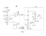
- FIG. 1 is a block diagram illustrating a configuration of an entire distance measuring apparatus according to an embodiment.
- FIG. 2 is a block diagram illustrating a configuration of a photodetector according to the first embodiment. It is a block diagram showing the structure of the photodetector of a 2nd embodiment. It is a block diagram showing the composition of the photodetector of a 3rd embodiment.
- FIG. 5 is a circuit diagram illustrating a configuration of a sample and hold circuit illustrated in FIG. 4. It is a block diagram showing the composition of the photodetector of a 4th embodiment. It is a block diagram showing the structure of the photodetector of a 5th embodiment. It is a block diagram showing the structure of the photodetector of a 6th embodiment.
- FIG. 8 is an explanatory diagram illustrating characteristics of the buffer circuit illustrated in FIGS.
- FIG. 9 is an explanatory diagram illustrating characteristics of the buffer circuit illustrated in FIGS.
- the distance measuring apparatus 100 is mounted on a vehicle, for example, and measures a distance to an obstacle around the vehicle. As shown in FIG. 1, a photodetector 1 and a light emitting unit 80 and a distance measuring unit 90.
- the light emitting section 80 emits signal light for distance measurement to the outside of the vehicle, and includes, for example, a light emitting diode that generates a laser beam as a light emitting element.
- the light emitting unit 80 causes the light emitting diode to emit light in response to the drive signal VLD input from the distance measuring unit 90, and emits a laser beam as a signal light in a predetermined direction via a predetermined optical system such as a lens. .
- the distance measuring section 90 includes a distance calculating section 92 and a time measuring section 94.
- Each of these units is configured by an electric circuit including a timer circuit, an arithmetic circuit, and the like.
- the distance calculation unit 92 outputs the drive signal VLD to the light emitting unit 80 at a predetermined distance measurement timing, and causes the light emitting unit 80 to emit signal light.
- the distance calculation unit 92 When the signal light is emitted from the light emitting unit 80, the distance calculation unit 92 outputs the drive signal V ON to the photodetector 1 after a predetermined delay time has elapsed, thereby activating the photodetector 1 and causing the signal light to start. Is started.
- the reason why the detection operation of the photodetector 1 is started after the elapse of the predetermined delay time is that the signal light emitted from the light emitting unit 80 is reflected directly or within the distance measuring device 100 to the photodetector 1. This is to prevent the detection signal from being output from the photodetector 1 when the light enters.
- Time measuring unit 94 measures a transmission pulse P S of the light emitting unit 80 is entered when emitted from the signal light, the time difference between the detection pulse P R that is input when the light detector 1 detects a signal light I do. That is, the time measuring unit 94 measures the time from when the signal light is emitted from the light emitting unit 80 until the signal light is reflected by the object to be measured and detected by the photodetector 1.
- the distance calculation unit 92 calculates the distance from the distance measurement device 100 to the object based on the time measured by the time measurement unit 94, and outputs the calculation result to another vehicle-mounted device such as a driving support device.
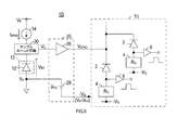
- the photodetector 1 is provided with a detection unit 10 having a plurality of SPADs 2 as detection SPADs.
- the input path of the detection pulse P R to the distance measuring unit 90 when the number of pulse signals output simultaneously from each SPAD2 detection unit 10 reaches a preset threshold or more, the signal light is detected and it determined to be, and outputs a detection pulse P R, the determination unit 70 is provided.
- the photodetector 1 includes a plurality of photodetectors 1A as illustrated in FIGS. 2 to 4 and FIGS. Since these photodetectors 1A to 1J will be described in the following description.
- the photodetector 1 ⁇ / b> A of the first embodiment includes a detection unit 10 having a plurality of SPADs 2 as detection SPADs, and a monitor having the same configuration and similar characteristics as the SPADs 2 in the detection unit 10. And a SPAD 12 for use.
- the SPAD 2 and the monitoring SPAD 12 are APDs that can operate in the Geiger mode as described above, and in the detection unit 10, the quenching elements 4 are connected to the cathodes of the plurality of SPADs 2, respectively.
- the quenching element 4 generates a voltage drop by a current flowing when a photon is incident on the SPAD 2 and the SPAD 2 is broken down, and stops the Geiger discharge of the SPAD 2.
- the quenching element 4 may be an element having a predetermined resistance value RQ , and may be configured by a resistance element that is a general passive element, or may be configured by an active element such as a transistor. Alternatively, in the present embodiment, an FET is used as shown by a dotted arrow in FIG.
- the quenching element 4 the input or stop of the driving signal V ON, the FET capable of switching conduction or interruption of the current path of the SPAD2 utilized .
- the quenching element 4 does not necessarily need to be configured by an FET to switch the operation or stop of the detection unit 10, and the quenching element 4 may be configured by a switching element other than the FET.
- a switching element may be provided in the power supply path to the detection unit 10 to switch on or off the power supply path to the detection unit 10 so as to switch the operation or stop of the detection unit 10.
- the pulse converter 6 is for outputting a pulse signal having a predetermined pulse width as a detection signal when a photon is incident on the corresponding SPAD 2.
- a current flows through the quenching element 4, the potential of the connection point is reduced.
- a digital pulse which becomes "1" when it is lowered is generated.
- each SPAD 2 depends on the temperature.
- the detection sensitivity changes.
- the photodetector 1A of the present embodiment based on the breakdown voltage V BD of the monitoring SPAD12 placed under the same environment and the detection unit 10, the reverse bias voltage applied to each SPAD2 in the detection unit 10 It is configured to be set.
- the photodetector 1A are both ends of a series circuit of a current source 14 supplies current to the monitor SPAD12, potential V A across the monitor SPAD12, based on V C, each SPAD2 and quenching element 4 And a drive unit 20 for setting each of the potentials.
- potential V A represents the potential of the anode of the monitor SPAD12
- potential V C represents the potential of the cathode of the monitor SPAD12.
- the current source 14 operates the monitor SPAD 12 in the Geiger mode by supplying a constant current I SPAD to the monitor SPAD 12 in the opposite direction, and supplies current to the anode of the monitor SPAD 12 and the monitor SPAD 12. It is provided between the negative electrode of the path. The cathode of the monitoring SPAD 12 is connected to the positive side of the current path.
- the monitoring SPAD 12 In order to supply a constant current I SPAD to the monitoring SPAD 12 via the current source 14, it is necessary to break down the monitoring SPAD 12 .
- light is generally incident on the monitoring SPAD 12.
- the monitoring SPAD 12 is provided with a light-shielding film 13 for preventing light from entering.
- the driving unit 20 determines the potentials of the anodes of the respective SPADs 2 and the detecting SPADs 2 of the quenching elements 4. Sets the potential on the opposite side.
- the driver 20, a first potential setting section of the present disclosure, the anode potential V A of the monitoring SPAD12, as a negative potential -V SPAD reverse bias voltage, a buffer circuit for applying to the anode of each SPAD2 22 are provided.
- the driver 20 as a second potential setting section of the present disclosure, the voltage source 24 to increase the cathode potential V C of the monitoring SPAD12 predetermined excess voltage V EX is provided. Then, the output from the voltage source 24, a positive potential V Q of the reverse bias voltage is applied to the opposite side of the SPAD2 of each quenching element 4 in the detection portion 10.
- the excess voltage V EX changes depending on the temperature of the SPAD2, as in the case where the reverse bias voltage applied to each SPAD2 in the detection unit 10 is constant. , The change of the photon detection sensitivity by the SPAD2 can be suppressed.
- the detection sensitivity of each SPAD 2 in the detection unit 10 is temperature-compensated, and the photodetection is performed at a desired detection sensitivity without being affected by the temperature change of each SPAD 2. Will be able to do it.
- the photodetector 1B according to the second embodiment includes a detection unit 10 having a plurality of SPADs 2 as detection SPADs, similar to the photodetector 1A according to the first embodiment. And a monitoring SPAD 12 having the same configuration and the same characteristics as the SPAD 2 of FIG.
- the quenching element 4 is connected to the anode of each SPAD 2 in the detection unit 10, and the pulse conversion unit 6 is connected to the connection point between each SPAD 2 and the quenching element 4. I have.
- the pulse converter 6 generates a digital pulse that becomes “1” when a photon enters the corresponding SPAD 2 and breaks down, and the potential at the connection point between the SPAD 2 and the quenching element 4 rises. .
- the photodetector 1B of the present embodiment also has a current source 14 for supplying a current to the monitoring SPAD 12 and each SPAD2 in the detection unit 10 and a quenching element, similarly to the photodetector 1A of the first embodiment. 4 is provided with a drive unit 20 for setting the potentials at both ends of the series circuit.
- the current source 14 is provided between the cathode of the monitoring SPAD 12 and the positive electrode of the current path to the monitoring SPAD 12, and the anode of the monitoring SPAD 12 is connected to the negative electrode of the current path.
- the light-shielding film 13 is provided on the monitoring SPAD 12 as in the photodetector 1A of the first embodiment.
- the driver 20 a third potential setting section of the present disclosure, the cathode potential V C of the monitoring SPAD12, a positive potential V SPAD reverse bias voltage, a buffer circuit for applying to the cathode of each SPAD2 26 are provided.
- a voltage source 28 to reduce the anode potential V A of the monitoring SPAD12 predetermined excess voltage V EX is provided. Then, the output from the voltage source 28 is applied as a negative potential ⁇ V Q of the reverse bias voltage to the opposite side of each quenching element 4 in the detection unit 10 from the SPAD 2.
- both ends of the series circuit of the respective SPAD2 and quenching element 4 in the detection portion 10 the breakdown voltage V BD of the monitoring SPAD12 A reverse bias voltage to which a predetermined excess voltage V EX is added is applied.
- the detection sensitivity of each SPAD2 in the detecting unit 10 is temperature compensated, and the influence of the temperature change of each SPAD2 is reduced.
- Light detection can be performed with a desired detection sensitivity without receiving light. For this reason, even if the distance measuring device 100 is configured using the photodetector 1B of the present embodiment, the distance measuring accuracy of the distance measuring device 100 can be stabilized.
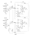
- the basic configuration of the photodetector 1C of the third embodiment is the same as that of the photodetector 1A of the first embodiment. The difference from the first embodiment is that, as shown in FIG. The point is that a sample and hold circuit 30 is provided at a connection portion with the current source 14.
- Sample-and-hold circuit 30 is temporarily conducting the cause of the current path to monitor SPAD12 including a current source 14, and holds the anode potential V A of the monitoring SPAD12, the retained potential V A, the driving unit 20 Is output to the buffer circuit 22.
- the sample-and-hold circuit 30 sets an energizing path between the anode of the monitoring SPAD 12 and the current source 14 and an output path of the potential VA from the energizing path to the buffer circuit 22.
- the switches 32 and 34 are semiconductor switches that can be turned on / off by inputting a switching signal from outside.
- a capacitor 36 connected to the anode of the monitoring SPAD and holding the anode potential VA when the switch 34 is on is provided on the output path of the potential VA from the switch 34 to the buffer circuit 22. Has been.
- the sample-and-hold circuit 30 turns on the switches 32 and 34 and applies a constant current I SPAD to the monitoring SPAD 12 in the opposite direction, thereby increasing the potential VA corresponding to the breakdown voltage of the monitoring SPAD 12. , And the capacitor 36.
- the switches 32 and 34 are periodically turned on, and the potential V of the anode when the monitoring SPAD 12 is broken down. A is held.
- the temperature of each SPAD 2 of the detection unit 10 can be compensated for by using the current source 14 without continuously flowing the constant current I SPAD to the monitoring SPAD 12 . It is possible to prevent the SPAD 12 from being deteriorated due to long-term continuous energization. For this reason, even if the distance measuring device 100 is configured using the photodetector 1C of the present embodiment, the distance measuring accuracy of the distance measuring device 100 can be stabilized.
- the basic configuration of the photodetector 1D of the fourth embodiment is the same as that of the photodetector 1B of the second embodiment. The difference from the second embodiment is that, as shown in FIG. The point is that a sample and hold circuit 30 is provided at a connection portion with the current source 14.
- This sample and hold circuit 30 is configured similarly to the sample and hold circuit 30 of the third embodiment shown in FIG.
- the sample hold circuit 30 is holding the cathode potential V C of the monitoring SPAD12, it outputs the potential V C, the buffer circuit 26 of the driving unit 20 Will be able to
- the photodetector 1E of the fifth embodiment has the same basic configuration as the photodetector 1A of the first embodiment, and differs from the first embodiment in that, as shown in FIG. Is divided into two groups 10a and 10b.
- the two groups 10a and 10b of the detection unit 10 are provided with a plurality of SPADs 2 and a quenching element 4 and a pulse conversion unit 6 connected to each SPAD 2, respectively.
- the groups 10a and 10b of the detection unit 10 are divided according to the arrangement positions of the SPADs 2 in the detection unit 10 so that, for example, adjacent SPADs 2 belong to the same group.
- the currents respectively connected to the two monitoring SPADs 12a, 12b and the anodes of the monitoring SPADs 12a, 12b correspond to the groups 10a, 10b of the detecting unit 10, respectively.
- Sources 14a, 14b are provided.
- the drive unit 20 applies the potentials V Aa and V Ab of the anodes of the monitoring SPADs 12a and 12b to the anodes of the SPADs 2 of the groups 10a and 10b, respectively, as the negative potential ⁇ V SPAD of the reverse bias voltage.
- Buffer circuits 22a and 22b are provided.
- the drive unit 20 is provided with a common voltage source 24 for each of the groups 10a and 10b. This is because the cathodes of the monitoring SPADs 12a and 12b are both connected to the positive electrode of the current supply path to the monitoring SPADs 12a and 12b, and the potentials V Ca and V Cb of the cathodes of the monitoring SPADs 12a and 12b are the same. That's why.
- a reverse bias voltage corresponding to the breakdown voltage of the monitoring SPADs 12a and 12b corresponding to the groups 10a and 10b is applied to the SPADs 2 of the groups 10a and 10b in the detection unit 10.
- the photodetector 1F according to the sixth embodiment has the same basic configuration as the photodetector 1B according to the second embodiment, and differs from the first embodiment only in the same manner as the fifth embodiment. Is divided into two groups 10a and 10b.
- the two groups 10a and 10b of the detection unit 10 are provided with a plurality of SPADs 2 and a quenching element 4 and a pulse conversion unit 6 connected to each SPAD 2, respectively.
- the currents connected to the two monitoring SPADs 12a, 12b and the cathodes of the monitoring SPADs 12a, 12b respectively correspond to the groups 10a, 10b of the detecting unit 10.
- Sources 14a, 14b are provided.
- the drive unit 20 applies the potentials V Ca and V Cb of the cathodes of the monitoring SPADs 12a and 12b to the cathodes of the SPADs 2 of the groups 10a and 10b as positive potentials V SPAD of reverse bias voltages, respectively.
- Buffer circuits 26a and 26b are provided.
- the drive unit 20 is provided with a common voltage source 28 for each of the groups 10a and 10b. Then, the SPAD2 of each group 10a, 10b quenching element 4 on the opposite side, the output from the voltage source 28 is applied as a negative potential -V Q of the bias voltage.
- the breakdown voltages of the monitoring SPADs 12a and 12b corresponding to the SPAD2 of each group 10a and 10b in the detection unit 10 are provided. Is applied.
- the photodetector 1G according to the seventh embodiment has the same basic configuration as the photodetector 1A according to the first embodiment.
- the difference from the first embodiment is that the driving unit 20 includes a first potential setting unit.
- the difference is that a potential setting section 40 for setting the potential -V SPAD applied to the anode of SPAD2 by calculation is provided.
- the potential setting unit 40 includes an A / D converter (hereinafter, ADC) 42, a microcomputer (hereinafter, MCU) 44 as an arithmetic unit, and a D / A converter (hereinafter, DAC) 46. I have.
- ADC A / D converter
- MCU microcomputer
- DAC D / A converter
- ADC42 is the anode potential V A of the monitoring SPAD12 converted A / D, the potential input to MCU44, MCU44 is that based on the digital data of the input voltage V A, is applied to the anode of each SPAD2 - Calculate V SPAD .
- This calculation estimates the temperature of the monitoring SPAD12 from the anode potential V A of the monitoring SPAD12, required to set the reverse bias voltage applied to each SPAD2 in accordance with the estimated temperature, the conversion map Is used.
- This conversion map absorbs the difference between the temperature characteristics of the breakdown voltage of the monitoring SPAD 12 and the temperature characteristics of the breakdown voltage of each SPAD 2, and calculates the potential ⁇ V SPAD applied to the anode of each SPAD 2 . It is set in advance so that it can be set appropriately.
- the calculation result of the potential ⁇ V SPAD calculated by the MCU 44 is input to the DAC 46, and the potential ⁇ V SPAD corresponding to the calculation result is applied from the DAC 46 to the anode of each SPAD 2 .
- each SPAD 2 is temperature-compensated and Can be prevented from changing due to temperature. Therefore, even when the distance measuring device 100 is configured using the photodetector 1G of the present embodiment, the distance measuring accuracy of the distance measuring device 100 can be stabilized.
- the drive unit 20 as a second potential setting section, than the cathode potential V C of the monitor SPAD12
- a voltage source 24 for setting a potential higher by the excess voltage V EX is provided.
- the potential setting section 40 can arbitrarily set the potential ⁇ V SPAD of the anode of each SPAD 2 in the detection section 10, and thus, for example, the potential V Q applied to the quenching element 4 of the detection section 10. and it may be set to the cathode the same potential V C of the monitoring SPAD12.
- the photodetector 1H according to the eighth embodiment has the same basic configuration as the photodetector 1B according to the second embodiment.
- the difference from the second embodiment is that the drive unit 20 includes a third potential setting unit.
- the difference is that a potential setting unit 50 for setting the potential V SPAD applied to the cathode of the SPAD 2 by calculation is provided.
- the potential setting unit 50 includes an ADC 52, an MCU 54 as a calculation unit, and a DAC 56, like the potential setting unit 40 of the seventh embodiment.
- ADC52 is the cathode potential V C of the monitoring SPAD12 converted A / D, input to MCU 54, MCU 54, based on the digital data of the input voltage V C, the potential V applied to the cathode of each SPAD2 Calculate SPAD .
- This calculation estimates the temperature of the monitoring SPAD12 from the cathode potential V C of the monitoring SPAD12, required to set the reverse bias voltage applied to each SPAD2 in accordance with the estimated temperature, the conversion map Is used.
- This conversion map absorbs the difference between the temperature characteristics of the breakdown voltage of the monitoring SPAD 12 and the temperature characteristics of the breakdown voltage of each SPAD 2, and makes the potential V SPAD applied to the cathode of each SPAD 2 more appropriate. Is set in advance so that it can be set to.
- the calculation result of the potential V SPAD calculated by the MCU 44 is input to the DAC 56, and the DAC 56 applies a potential V SPAD corresponding to the calculation result to the cathode of each SPAD 2 .
- each SPAD 2 is temperature-compensated and the photon is compensated. Can be prevented from changing due to temperature. Therefore, even when the distance measuring device 100 is configured using the photodetector 1H of the present embodiment, the distance measuring accuracy of the distance measuring device 100 can be stabilized.
- the drive unit 20 as a fourth potential setting section, the anode of the monitoring SPAD12 potential V A A voltage source 24 for setting a potential lower by the excess voltage V EX than the voltage source 24 is provided.
- the potential setting unit 50 can arbitrarily set the potential V SPAD of the cathode of each SPAD 2 in the detection unit 10. Therefore, for example, the potential ⁇ V Q applied to the quenching element 4 of the detection unit 10. and it may be set to the cathode the same potential V C of the monitoring SPAD12.
- the photodetector 1I according to the ninth embodiment has the same basic configuration as the photodetector 1G according to the seventh embodiment.
- the difference from the seventh embodiment is that the potential setting unit 40 uses the SPAD2, the quenching element 4, The positive and negative potentials V Q and ⁇ V SPAD applied to both ends of the series circuit are set by calculation.
- the potential setting section 40 of the present embodiment includes a ADC 42, and MCU48, a DAC 46, MCU48, based on the anode potential V A of the monitor SPAD12 input from ADC 42, The positive / negative potentials V Q and ⁇ V SPAD are calculated.
- the calculation result of the potential ⁇ V SPAD calculated by the MCU 48 is input to the DAC 46, and the potential ⁇ V SPAD corresponding to the calculation result is applied from the DAC 46 to the anode of each SPAD 2 .
- the drive unit 20 instead of the voltage source 24, D / A converter (DAC) 49 is provided, the operation result of the computed potential V Q at MCU48 is input to the DAC 49. Then, DAC 49 is the potential V Q corresponding to the operation result is applied to the opposite side of the SPAD2 quenching element 4.
- DAC D / A converter
- the photodetector 1I of the present embodiment similarly to the photodetector 1G of the seventh embodiment, the temperature characteristics of the monitoring SPAD 12 and the temperature characteristics of each SPAD2 in the detection unit 10 are different. Even so, each SPAD 2 can be temperature compensated. Therefore, even when the distance measuring device 100 is configured using the photodetector 1I of the present embodiment, the distance measuring accuracy of the distance measuring device 100 can be stabilized.
- the photodetector 1J according to the tenth embodiment has the same basic configuration as the photodetector 1H according to the eighth embodiment.
- the difference from the eighth embodiment is that the potential setting unit 50 uses the SPAD2, the quenching element 4, Is to set the positive and negative potentials V SPAD , ⁇ V Q applied to both ends of the series circuit by calculation.
- the calculation result of the potential V SPAD calculated by the MCU 48 is input to the DAC 56, and the DAC 56 applies a potential V SPAD corresponding to the calculation result to the cathode of each SPAD 2 .
- the drive unit 20 instead of the voltage source 28, D / A converter (DAC) 59 is provided, the operation result of the computed potential -V Q at MCU58 is input to the DAC 49. Then, the DAC 49 applies the potential ⁇ V Q corresponding to the calculation result to the opposite side of the quenching element 4 from the SPAD 2.
- DAC D / A converter
- the temperature characteristic of the monitoring SPAD 12 and the temperature characteristic of each SPAD2 in the detection unit 10 are different. Even so, each SPAD 2 can be temperature compensated. Therefore, even when the distance measuring device 100 is configured using the photodetector 1J of the present embodiment, the distance measuring accuracy of the distance measuring device 100 can be stabilized.
- MCU58 as an arithmetic unit, based on the potential of the cathode V C of the monitoring SPAD12, positive and negative potentials V SPAD, since setting the -V Q, the reverse bias voltage Can be simplified.
- the photodetector 1A of the first embodiment shown in FIG. 2 and the photodetectors 1C and 1E of the third and fifth embodiments, which are modifications thereof, are connected to the anode of the SPAD2 in the detection unit 10 with a monitor.
- a buffer circuit 22 for applying the potential VA of the anode of the SPAD 12 is provided.
- the buffer circuit is generally constituted by an amplifier circuit having an amplification factor of “1”, and the potential of the output terminal matches the potential of the input terminal.
- the buffer circuit 22 if configured by an amplifier circuit amplification factor "1", to the anode of SPAD2 in the detection unit 10, the anode potential V A of the monitoring SPAD12, reverse bias
- the voltage can be applied as a negative potential -V SPAD .
- the SPAD2 in the detection unit 10 always becomes a reverse bias voltage is applied greater than the breakdown voltage V BD of the monitoring SPAD12.
- the buffer circuit 22 changes the anode potential V of the monitoring SPAD 12 when the breakdown voltage V BD is equal to the threshold voltage V BDth.
- A may be configured to be output.
- the breakdown voltage V BD of the monitoring SPAD 12 is equal to or higher than the threshold voltage V BDth , the negative potential ⁇ V SPAD of the reverse bias voltage is set, and the breakdown voltage V BD is set to the threshold voltage V BDth .
- the anode of the monitor SPAD12 of potential V a of the time can be fixed to
- the negative potential ⁇ V SPAD of the reverse bias voltage becomes too low due to the temperature change, and the reverse bias voltage applied to the SPAD 2 in the detection unit 10 becomes an overvoltage, and the SPAD 2 becomes Deterioration can be suppressed.
- the breakdown voltage V BD of the monitoring SPAD12 is lower than the threshold voltage V BDth is similar to the above embodiments, the anode potential V A of the monitoring SPAD12, outputs a negative potential -V SPAD reverse bias voltage Thus, the temperature of the SPAD 2 can be compensated.
- the buffer circuit 26 has the amplification factor “1”.
- An amplifier circuit may be used, or a circuit having the characteristics shown in FIG.
- the buffer circuit 26 sets the potential of the cathode of the monitoring SPAD 12 when the breakdown voltage V BD is equal to the threshold voltage V BDth. it may be configured to output a V C.
- the cathode of the monitoring SPAD12 of can be fixed to the potential V C.
- the positive potential V SPAD of the reverse bias voltage becomes too high due to the temperature change, and the reverse bias voltage applied to the SPAD 2 in the detection unit 10 becomes an overvoltage, and the SPAD 2 is deteriorated. Can be suppressed.
- the cathode of the monitoring SPAD12 potential V C when the breakdown voltage V BD of the monitoring SPAD12 is lower than the threshold voltage V BDth is similar to the above embodiment, the cathode of the monitoring SPAD12 potential V C, and outputs a positive potential V SPAD reverse bias voltage
- SPAD2 can be temperature compensated.
- the buffer circuits 22 and 26 are set so that the amplification factor is “1” and the breakdown voltage V BD of the monitoring SPAD 12 is equal to the threshold value.
- An amplifier circuit that saturates when the voltage becomes higher than the voltage VBDth may be used.
- the buffer circuits 22 and 26 have an amplification circuit having an amplification factor of “1” and an output from the amplification circuit is equal to or higher than the potential when the breakdown voltage V BD of the monitoring SPAD 12 is equal to the threshold voltage V BDth.
- a holding circuit for holding the output at that potential may be used.
- the detection unit 10 is described as being provided with a plurality of SPADs 2.
- the configuration described above may be employed.
- the light-shielding film 13 for preventing light from being incident on the monitor SPAD 12 has been described.
- the light-shielding film 13 is not necessarily provided. Light may be prevented from entering.
- a plurality of functions of one component in the above embodiment may be realized by a plurality of components, or one function of one component may be realized by a plurality of components.
- a plurality of functions of a plurality of components may be realized by one component, or one function realized by a plurality of components may be realized by one component.
- a part of the configuration of the above embodiment may be omitted.
- at least a part of the configuration of the above-described embodiment may be added to or replaced with the configuration of another above-described embodiment.
Landscapes
- Engineering & Computer Science (AREA)
- Physics & Mathematics (AREA)
- General Physics & Mathematics (AREA)
- Radar, Positioning & Navigation (AREA)
- Remote Sensing (AREA)
- Computer Networks & Wireless Communication (AREA)
- Multimedia (AREA)
- Signal Processing (AREA)
- Electromagnetism (AREA)
- Measurement Of Optical Distance (AREA)
- Optical Radar Systems And Details Thereof (AREA)
- Light Receiving Elements (AREA)
Applications Claiming Priority (2)
| Application Number | Priority Date | Filing Date | Title |
|---|---|---|---|
| JP2018118821A JP6835042B2 (ja) | 2018-06-22 | 2018-06-22 | 測距装置 |
| JP2018-118821 | 2018-06-22 |
Publications (1)
| Publication Number | Publication Date |
|---|---|
| WO2019245034A1 true WO2019245034A1 (ja) | 2019-12-26 |
Family
ID=68984067
Family Applications (1)
| Application Number | Title | Priority Date | Filing Date |
|---|---|---|---|
| PCT/JP2019/024745 Ceased WO2019245034A1 (ja) | 2018-06-22 | 2019-06-21 | 測距装置 |
Country Status (2)
| Country | Link |
|---|---|
| JP (1) | JP6835042B2 (https=) |
| WO (1) | WO2019245034A1 (https=) |
Families Citing this family (1)
| Publication number | Priority date | Publication date | Assignee | Title |
|---|---|---|---|---|
| WO2025263207A1 (ja) * | 2024-06-18 | 2025-12-26 | ソニーセミコンダクタソリューションズ株式会社 | 電圧検出回路および光検出装置 |
Citations (8)
| Publication number | Priority date | Publication date | Assignee | Title |
|---|---|---|---|---|
| JP2012519843A (ja) * | 2009-03-06 | 2012-08-30 | コーニンクレッカ フィリップス エレクトロニクス エヌ ヴィ | 単一光子カウンタのための高度な温度報償及び制御回路 |
| JP2013016638A (ja) * | 2011-07-04 | 2013-01-24 | Hamamatsu Photonics Kk | フォトダイオードアレイモジュール |
| US20140231630A1 (en) * | 2013-02-18 | 2014-08-21 | Stmicroelectronics (Research & Development) Limited | Method and apparatus for image sensor calibration |
| JP2014216531A (ja) * | 2013-04-26 | 2014-11-17 | 株式会社東芝 | 光検出装置、放射線検出装置、放射線分析装置及び光検出方法 |
| JP2015078953A (ja) * | 2013-10-18 | 2015-04-23 | 株式会社デンソー | レーダ装置 |
| JP2016061729A (ja) * | 2014-09-19 | 2016-04-25 | 株式会社東芝 | 光子検出素子、光子検出装置、及び放射線分析装置 |
| CN105988497A (zh) * | 2015-01-30 | 2016-10-05 | 财团法人工业技术研究院 | 单光子雪崩光电二极管的超额偏压控制系统与方法 |
| WO2017180277A1 (en) * | 2016-04-15 | 2017-10-19 | Qualcomm Incorporated | Active area selection for lidar receivers |
-
2018
- 2018-06-22 JP JP2018118821A patent/JP6835042B2/ja active Active
-
2019
- 2019-06-21 WO PCT/JP2019/024745 patent/WO2019245034A1/ja not_active Ceased
Patent Citations (8)
| Publication number | Priority date | Publication date | Assignee | Title |
|---|---|---|---|---|
| JP2012519843A (ja) * | 2009-03-06 | 2012-08-30 | コーニンクレッカ フィリップス エレクトロニクス エヌ ヴィ | 単一光子カウンタのための高度な温度報償及び制御回路 |
| JP2013016638A (ja) * | 2011-07-04 | 2013-01-24 | Hamamatsu Photonics Kk | フォトダイオードアレイモジュール |
| US20140231630A1 (en) * | 2013-02-18 | 2014-08-21 | Stmicroelectronics (Research & Development) Limited | Method and apparatus for image sensor calibration |
| JP2014216531A (ja) * | 2013-04-26 | 2014-11-17 | 株式会社東芝 | 光検出装置、放射線検出装置、放射線分析装置及び光検出方法 |
| JP2015078953A (ja) * | 2013-10-18 | 2015-04-23 | 株式会社デンソー | レーダ装置 |
| JP2016061729A (ja) * | 2014-09-19 | 2016-04-25 | 株式会社東芝 | 光子検出素子、光子検出装置、及び放射線分析装置 |
| CN105988497A (zh) * | 2015-01-30 | 2016-10-05 | 财团法人工业技术研究院 | 单光子雪崩光电二极管的超额偏压控制系统与方法 |
| WO2017180277A1 (en) * | 2016-04-15 | 2017-10-19 | Qualcomm Incorporated | Active area selection for lidar receivers |
Also Published As
| Publication number | Publication date |
|---|---|
| JP6835042B2 (ja) | 2021-02-24 |
| JP2019219345A (ja) | 2019-12-26 |
Similar Documents
| Publication | Publication Date | Title |
|---|---|---|
| US11296241B2 (en) | Light detector having monitoring single photon avalanche diode (SPAD) | |
| CN110462847B (zh) | 光检测器 | |
| US7907061B2 (en) | Proximity sensors and methods for sensing proximity | |
| US8207488B2 (en) | Photodetector circuit | |
| JP5644294B2 (ja) | 光検出器 | |
| WO2019194039A1 (ja) | 光測距装置 | |
| JP2016225453A (ja) | 光センサ | |
| JP6643270B2 (ja) | 光検出器 | |
| JP6835042B2 (ja) | 測距装置 | |
| JP2001024272A (ja) | 半導体レーザの劣化判定回路 | |
| US20070098027A1 (en) | Light-emitting element driver | |
| JP6969504B2 (ja) | 測距装置 | |
| CN210141940U (zh) | 单光子探测器及其高压快速调节电路 | |
| JP6614684B2 (ja) | 電磁波検出装置 | |
| US11199439B2 (en) | Photodetector device and optical encoder device | |
| JP7853871B2 (ja) | 光センサ | |
| TW202139600A (zh) | 峰值偵測器電路及用於評估第一輸入電壓之峰值的方法 | |
| JP3930621B2 (ja) | 測距モジュール | |
| US11194026B2 (en) | Light detection device | |
| WO2025141966A1 (ja) | 光検出器および光検出装置 | |
| KR20240037091A (ko) | 포토 다이오드의 방전 상태를 모니터링하는 전자 장치 및 이의 제어 방법 | |
| JP2019219345A5 (https=) | ||
| JPS63289978A (ja) | 半導体レ−ザ−劣化検出回路 | |
| WO2023037611A1 (ja) | 駆動装置、駆動方法及び発光装置 | |
| KR20240037092A (ko) | 포토 다이오드의 방전을 제어하는 전자 장치 및 이의 제어 방법 |
Legal Events
| Date | Code | Title | Description |
|---|---|---|---|
| 121 | Ep: the epo has been informed by wipo that ep was designated in this application |
Ref document number: 19822093 Country of ref document: EP Kind code of ref document: A1 |
|
| NENP | Non-entry into the national phase |
Ref country code: DE |
|
| 122 | Ep: pct application non-entry in european phase |
Ref document number: 19822093 Country of ref document: EP Kind code of ref document: A1 |