WO2019245034A1 - Distance measuring device - Google Patents
Distance measuring device Download PDFInfo
- Publication number
- WO2019245034A1 WO2019245034A1 PCT/JP2019/024745 JP2019024745W WO2019245034A1 WO 2019245034 A1 WO2019245034 A1 WO 2019245034A1 JP 2019024745 W JP2019024745 W JP 2019024745W WO 2019245034 A1 WO2019245034 A1 WO 2019245034A1
- Authority
- WO
- WIPO (PCT)
- Prior art keywords
- spad
- potential
- detection
- monitoring
- distance measuring
- Prior art date
Links
- 238000001514 detection method Methods 0.000 claims abstract description 146
- 238000012544 monitoring process Methods 0.000 claims abstract description 110
- 238000010791 quenching Methods 0.000 claims abstract description 52
- 230000000171 quenching effect Effects 0.000 claims abstract description 51
- 230000015556 catabolic process Effects 0.000 claims description 42
- 238000005259 measurement Methods 0.000 claims description 13
- 230000035945 sensitivity Effects 0.000 description 18
- 238000010586 diagram Methods 0.000 description 14
- 230000003321 amplification Effects 0.000 description 10
- 238000006243 chemical reaction Methods 0.000 description 10
- 238000003199 nucleic acid amplification method Methods 0.000 description 10
- 230000003287 optical effect Effects 0.000 description 7
- 239000000203 mixture Substances 0.000 description 4
- 239000003990 capacitor Substances 0.000 description 3
- 238000012986 modification Methods 0.000 description 3
- 230000004048 modification Effects 0.000 description 3
- 238000000098 azimuthal photoelectron diffraction Methods 0.000 description 2
- 238000000034 method Methods 0.000 description 2
- 230000003213 activating effect Effects 0.000 description 1
- 230000005540 biological transmission Effects 0.000 description 1
- 230000000903 blocking effect Effects 0.000 description 1
- 230000006866 deterioration Effects 0.000 description 1
- 238000002347 injection Methods 0.000 description 1
- 239000007924 injection Substances 0.000 description 1
- 230000007774 longterm Effects 0.000 description 1
- 230000000717 retained effect Effects 0.000 description 1
- 239000004065 semiconductor Substances 0.000 description 1
Images


Classifications
-
- G—PHYSICS
- G01—MEASURING; TESTING
- G01C—MEASURING DISTANCES, LEVELS OR BEARINGS; SURVEYING; NAVIGATION; GYROSCOPIC INSTRUMENTS; PHOTOGRAMMETRY OR VIDEOGRAMMETRY
- G01C3/00—Measuring distances in line of sight; Optical rangefinders
- G01C3/02—Details
- G01C3/06—Use of electric means to obtain final indication
-
- G—PHYSICS
- G01—MEASURING; TESTING
- G01S—RADIO DIRECTION-FINDING; RADIO NAVIGATION; DETERMINING DISTANCE OR VELOCITY BY USE OF RADIO WAVES; LOCATING OR PRESENCE-DETECTING BY USE OF THE REFLECTION OR RERADIATION OF RADIO WAVES; ANALOGOUS ARRANGEMENTS USING OTHER WAVES
- G01S7/00—Details of systems according to groups G01S13/00, G01S15/00, G01S17/00
- G01S7/48—Details of systems according to groups G01S13/00, G01S15/00, G01S17/00 of systems according to group G01S17/00
- G01S7/483—Details of pulse systems
- G01S7/486—Receivers
-
- G—PHYSICS
- G01—MEASURING; TESTING
- G01S—RADIO DIRECTION-FINDING; RADIO NAVIGATION; DETERMINING DISTANCE OR VELOCITY BY USE OF RADIO WAVES; LOCATING OR PRESENCE-DETECTING BY USE OF THE REFLECTION OR RERADIATION OF RADIO WAVES; ANALOGOUS ARRANGEMENTS USING OTHER WAVES
- G01S7/00—Details of systems according to groups G01S13/00, G01S15/00, G01S17/00
- G01S7/48—Details of systems according to groups G01S13/00, G01S15/00, G01S17/00 of systems according to group G01S17/00
- G01S7/497—Means for monitoring or calibrating
-
- H—ELECTRICITY
- H01—ELECTRIC ELEMENTS
- H01L—SEMICONDUCTOR DEVICES NOT COVERED BY CLASS H10
- H01L31/00—Semiconductor devices sensitive to infrared radiation, light, electromagnetic radiation of shorter wavelength or corpuscular radiation and specially adapted either for the conversion of the energy of such radiation into electrical energy or for the control of electrical energy by such radiation; Processes or apparatus specially adapted for the manufacture or treatment thereof or of parts thereof; Details thereof
- H01L31/08—Semiconductor devices sensitive to infrared radiation, light, electromagnetic radiation of shorter wavelength or corpuscular radiation and specially adapted either for the conversion of the energy of such radiation into electrical energy or for the control of electrical energy by such radiation; Processes or apparatus specially adapted for the manufacture or treatment thereof or of parts thereof; Details thereof in which radiation controls flow of current through the device, e.g. photoresistors
- H01L31/10—Semiconductor devices sensitive to infrared radiation, light, electromagnetic radiation of shorter wavelength or corpuscular radiation and specially adapted either for the conversion of the energy of such radiation into electrical energy or for the control of electrical energy by such radiation; Processes or apparatus specially adapted for the manufacture or treatment thereof or of parts thereof; Details thereof in which radiation controls flow of current through the device, e.g. photoresistors characterised by at least one potential-jump barrier or surface barrier, e.g. phototransistors
- H01L31/101—Devices sensitive to infrared, visible or ultraviolet radiation
- H01L31/102—Devices sensitive to infrared, visible or ultraviolet radiation characterised by only one potential barrier or surface barrier
- H01L31/107—Devices sensitive to infrared, visible or ultraviolet radiation characterised by only one potential barrier or surface barrier the potential barrier working in avalanche mode, e.g. avalanche photodiode
Definitions
- the present disclosure relates to a distance measuring device that measures a distance from an emission of a signal light for distance measurement to a time at which the signal light is reflected upon the object, thereby measuring a distance to the object.
- This type of distance measuring device usually emits a signal light from a light emitting unit that emits signal light for distance measurement, a photodetector that detects reflected light that has been reflected by the signal light hitting an object, and a light emitting unit. Thereafter, the distance measuring unit measures the time until the reflected light is detected by the photodetector.
- SPAD is an abbreviation for Single Photon Avalanche Diode, and is an avalanche photodiode (APD) that operates in Geiger mode.
- APD avalanche photodiode
- SPADs have higher light receiving sensitivity than general photodiodes (PDs) and APDs. Therefore, in the distance measuring device proposed above, reflected light is more accurately reflected by using SPADs as photodetectors. Detection is performed to ensure distance measurement accuracy.
- the detection sensitivity of APD and SPAD greatly changes according to the temperature.
- Patent Document 2 in a photodetector using an APD, in order to perform temperature compensation of the APD, the temperature characteristic of the current amplification factor is substantially the same as that of the APD, and a reverse biased reference is used. It has been proposed to make use of a bonding structure.
- the photodetector described in Patent Document 2 uses a transistor having a junction for current injection for injecting a reference current into the junction for reference, and uses the APD and the reference so as to maintain the amplification factor of the reference current at a predetermined value.
- the multiplication factor of the APD is controlled by controlling the voltage applied to the bonding structure.
- JP 2017-75906 A Japanese Patent No. 5211095
- Patent Document 1 cannot be applied to an APD operating in a Kaiger mode, that is, a photodetector provided with a SPAD, as an element for photodetection. , Was found.
- the reverse bias voltage is set to a voltage value higher than the breakdown voltage. Since the SPAD breaks down in response to the incidence of photons, the photodetector using the SPAD is configured to output a pulse signal having a predetermined pulse width when the SPAD breaks down.
- One aspect of the present disclosure is a distance measurement device configured to detect a signal light for distance measurement using a photodetector including a SPAD, by temperature-compensating the sensitivity of detection of photons by the SPAD, It is desirable to suppress fluctuation in distance measurement accuracy due to temperature.
- the distance measuring apparatus includes a light emitting unit that emits a signal light for distance measurement, a photodetector that detects the signal light, and a distance measuring unit.
- the distance measuring unit emits the signal light from the light emitting unit, measures the time until the emitted signal light is reflected by the object and detected by the photodetector, and based on the measured time, , Calculate the distance to the object.
- the photodetector also includes a detection unit, a monitoring SPAD, a current source, and a driving unit.
- the detection unit includes a detection SPAD, which is an avalanche photodiode operable in Geiger mode, and a quenching element connected in series to the detection SPAD.
- the quenching element is used to stop the detection SPAD from breaking down due to the incidence of photons and causing Geiger discharge.
- the detection unit outputs, as a detection signal, a change in potential at a connection point between the detection SPAD and the quenching element, which occurs when the detection SPAD is broken down by the incidence of photons.
- the monitor SPAD is a SPAD having the same characteristics as the SPAD constituting the detection unit, operates in a Geiger mode when a constant current is supplied from a current source, and generates a breakdown voltage at both ends. This breakdown voltage changes in accordance with the temperature of the monitoring SPAD, and for example, increases as the temperature increases.
- the driving unit is configured to control the series circuit of the detection SPAD and the quenching element in the detection unit based on the potential at both ends of the monitoring SPAD or the potential on the current source side of the monitoring SPAD. Set the potential at both ends of.
- the drive unit obtains the potential at both ends of the monitoring SPAD or the current source side as a parameter representing the breakdown voltage of the detection SPAD, and sets the potential at both ends of the series circuit of the detection SPAD and the quenching element. I do.
- the reverse bias voltage applied to the detection SPAD via the quenching element is set to a voltage corresponding to the breakdown voltage of the monitoring SPAD and applied to a series circuit of the quenching element and the detection SPAD. can do.
- the voltage applied to the series circuit is applied to the detection SPAD as a reverse bias voltage for photon detection until a photon enters the detection SPAD and a current flows through the quenching element.
- the photodetector of the present disclosure as in the case where the reverse bias voltage is set to a constant voltage, the excess voltage obtained by subtracting the breakdown voltage from the reverse bias voltage changes according to the temperature of the detection SPAD. Can be suppressed.
- the photodetector of the present disclosure it is possible to suppress a change in the detection sensitivity of the detection SPAD due to a change in the excess voltage due to a temperature change. That is, according to the photodetector of the present disclosure, the detection sensitivity of the detection SPAD is temperature-compensated, and the light detection can be performed at a desired detection sensitivity without being affected by the temperature change of the detection SPAD. Become.
- the ranging device of the present disclosure it is possible to suppress the variation in the ranging accuracy due to the change in the detection sensitivity of the detection SPAD constituting the photodetector, and to stabilize the ranging accuracy. Can be.
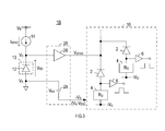
- FIG. 1 is a block diagram illustrating a configuration of an entire distance measuring apparatus according to an embodiment.
- FIG. 2 is a block diagram illustrating a configuration of a photodetector according to the first embodiment. It is a block diagram showing the structure of the photodetector of a 2nd embodiment. It is a block diagram showing the composition of the photodetector of a 3rd embodiment.
- FIG. 5 is a circuit diagram illustrating a configuration of a sample and hold circuit illustrated in FIG. 4. It is a block diagram showing the composition of the photodetector of a 4th embodiment. It is a block diagram showing the structure of the photodetector of a 5th embodiment. It is a block diagram showing the structure of the photodetector of a 6th embodiment.
- FIG. 8 is an explanatory diagram illustrating characteristics of the buffer circuit illustrated in FIGS.
- FIG. 9 is an explanatory diagram illustrating characteristics of the buffer circuit illustrated in FIGS.
- the distance measuring apparatus 100 is mounted on a vehicle, for example, and measures a distance to an obstacle around the vehicle. As shown in FIG. 1, a photodetector 1 and a light emitting unit 80 and a distance measuring unit 90.
- the light emitting section 80 emits signal light for distance measurement to the outside of the vehicle, and includes, for example, a light emitting diode that generates a laser beam as a light emitting element.
- the light emitting unit 80 causes the light emitting diode to emit light in response to the drive signal VLD input from the distance measuring unit 90, and emits a laser beam as a signal light in a predetermined direction via a predetermined optical system such as a lens. .
- the distance measuring section 90 includes a distance calculating section 92 and a time measuring section 94.
- Each of these units is configured by an electric circuit including a timer circuit, an arithmetic circuit, and the like.
- the distance calculation unit 92 outputs the drive signal VLD to the light emitting unit 80 at a predetermined distance measurement timing, and causes the light emitting unit 80 to emit signal light.
- the distance calculation unit 92 When the signal light is emitted from the light emitting unit 80, the distance calculation unit 92 outputs the drive signal V ON to the photodetector 1 after a predetermined delay time has elapsed, thereby activating the photodetector 1 and causing the signal light to start. Is started.
- the reason why the detection operation of the photodetector 1 is started after the elapse of the predetermined delay time is that the signal light emitted from the light emitting unit 80 is reflected directly or within the distance measuring device 100 to the photodetector 1. This is to prevent the detection signal from being output from the photodetector 1 when the light enters.
- Time measuring unit 94 measures a transmission pulse P S of the light emitting unit 80 is entered when emitted from the signal light, the time difference between the detection pulse P R that is input when the light detector 1 detects a signal light I do. That is, the time measuring unit 94 measures the time from when the signal light is emitted from the light emitting unit 80 until the signal light is reflected by the object to be measured and detected by the photodetector 1.
- the distance calculation unit 92 calculates the distance from the distance measurement device 100 to the object based on the time measured by the time measurement unit 94, and outputs the calculation result to another vehicle-mounted device such as a driving support device.
- the photodetector 1 is provided with a detection unit 10 having a plurality of SPADs 2 as detection SPADs.
- the input path of the detection pulse P R to the distance measuring unit 90 when the number of pulse signals output simultaneously from each SPAD2 detection unit 10 reaches a preset threshold or more, the signal light is detected and it determined to be, and outputs a detection pulse P R, the determination unit 70 is provided.
- the photodetector 1 includes a plurality of photodetectors 1A as illustrated in FIGS. 2 to 4 and FIGS. Since these photodetectors 1A to 1J will be described in the following description.
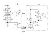
- the photodetector 1 ⁇ / b> A of the first embodiment includes a detection unit 10 having a plurality of SPADs 2 as detection SPADs, and a monitor having the same configuration and similar characteristics as the SPADs 2 in the detection unit 10. And a SPAD 12 for use.
- the SPAD 2 and the monitoring SPAD 12 are APDs that can operate in the Geiger mode as described above, and in the detection unit 10, the quenching elements 4 are connected to the cathodes of the plurality of SPADs 2, respectively.
- the quenching element 4 generates a voltage drop by a current flowing when a photon is incident on the SPAD 2 and the SPAD 2 is broken down, and stops the Geiger discharge of the SPAD 2.
- the quenching element 4 may be an element having a predetermined resistance value RQ , and may be configured by a resistance element that is a general passive element, or may be configured by an active element such as a transistor. Alternatively, in the present embodiment, an FET is used as shown by a dotted arrow in FIG.
- the quenching element 4 the input or stop of the driving signal V ON, the FET capable of switching conduction or interruption of the current path of the SPAD2 utilized .
- the quenching element 4 does not necessarily need to be configured by an FET to switch the operation or stop of the detection unit 10, and the quenching element 4 may be configured by a switching element other than the FET.
- a switching element may be provided in the power supply path to the detection unit 10 to switch on or off the power supply path to the detection unit 10 so as to switch the operation or stop of the detection unit 10.
- the pulse converter 6 is for outputting a pulse signal having a predetermined pulse width as a detection signal when a photon is incident on the corresponding SPAD 2.
- a current flows through the quenching element 4, the potential of the connection point is reduced.
- a digital pulse which becomes "1" when it is lowered is generated.
- each SPAD 2 depends on the temperature.
- the detection sensitivity changes.
- the photodetector 1A of the present embodiment based on the breakdown voltage V BD of the monitoring SPAD12 placed under the same environment and the detection unit 10, the reverse bias voltage applied to each SPAD2 in the detection unit 10 It is configured to be set.
- the photodetector 1A are both ends of a series circuit of a current source 14 supplies current to the monitor SPAD12, potential V A across the monitor SPAD12, based on V C, each SPAD2 and quenching element 4 And a drive unit 20 for setting each of the potentials.
- potential V A represents the potential of the anode of the monitor SPAD12
- potential V C represents the potential of the cathode of the monitor SPAD12.
- the current source 14 operates the monitor SPAD 12 in the Geiger mode by supplying a constant current I SPAD to the monitor SPAD 12 in the opposite direction, and supplies current to the anode of the monitor SPAD 12 and the monitor SPAD 12. It is provided between the negative electrode of the path. The cathode of the monitoring SPAD 12 is connected to the positive side of the current path.
- the monitoring SPAD 12 In order to supply a constant current I SPAD to the monitoring SPAD 12 via the current source 14, it is necessary to break down the monitoring SPAD 12 .
- light is generally incident on the monitoring SPAD 12.
- the monitoring SPAD 12 is provided with a light-shielding film 13 for preventing light from entering.
- the driving unit 20 determines the potentials of the anodes of the respective SPADs 2 and the detecting SPADs 2 of the quenching elements 4. Sets the potential on the opposite side.
- the driver 20, a first potential setting section of the present disclosure, the anode potential V A of the monitoring SPAD12, as a negative potential -V SPAD reverse bias voltage, a buffer circuit for applying to the anode of each SPAD2 22 are provided.
- the driver 20 as a second potential setting section of the present disclosure, the voltage source 24 to increase the cathode potential V C of the monitoring SPAD12 predetermined excess voltage V EX is provided. Then, the output from the voltage source 24, a positive potential V Q of the reverse bias voltage is applied to the opposite side of the SPAD2 of each quenching element 4 in the detection portion 10.
- the excess voltage V EX changes depending on the temperature of the SPAD2, as in the case where the reverse bias voltage applied to each SPAD2 in the detection unit 10 is constant. , The change of the photon detection sensitivity by the SPAD2 can be suppressed.
- the detection sensitivity of each SPAD 2 in the detection unit 10 is temperature-compensated, and the photodetection is performed at a desired detection sensitivity without being affected by the temperature change of each SPAD 2. Will be able to do it.
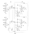
- the photodetector 1B according to the second embodiment includes a detection unit 10 having a plurality of SPADs 2 as detection SPADs, similar to the photodetector 1A according to the first embodiment. And a monitoring SPAD 12 having the same configuration and the same characteristics as the SPAD 2 of FIG.
- the quenching element 4 is connected to the anode of each SPAD 2 in the detection unit 10, and the pulse conversion unit 6 is connected to the connection point between each SPAD 2 and the quenching element 4. I have.
- the pulse converter 6 generates a digital pulse that becomes “1” when a photon enters the corresponding SPAD 2 and breaks down, and the potential at the connection point between the SPAD 2 and the quenching element 4 rises. .
- the photodetector 1B of the present embodiment also has a current source 14 for supplying a current to the monitoring SPAD 12 and each SPAD2 in the detection unit 10 and a quenching element, similarly to the photodetector 1A of the first embodiment. 4 is provided with a drive unit 20 for setting the potentials at both ends of the series circuit.
- the current source 14 is provided between the cathode of the monitoring SPAD 12 and the positive electrode of the current path to the monitoring SPAD 12, and the anode of the monitoring SPAD 12 is connected to the negative electrode of the current path.
- the light-shielding film 13 is provided on the monitoring SPAD 12 as in the photodetector 1A of the first embodiment.
- the driver 20 a third potential setting section of the present disclosure, the cathode potential V C of the monitoring SPAD12, a positive potential V SPAD reverse bias voltage, a buffer circuit for applying to the cathode of each SPAD2 26 are provided.
- a voltage source 28 to reduce the anode potential V A of the monitoring SPAD12 predetermined excess voltage V EX is provided. Then, the output from the voltage source 28 is applied as a negative potential ⁇ V Q of the reverse bias voltage to the opposite side of each quenching element 4 in the detection unit 10 from the SPAD 2.
- both ends of the series circuit of the respective SPAD2 and quenching element 4 in the detection portion 10 the breakdown voltage V BD of the monitoring SPAD12 A reverse bias voltage to which a predetermined excess voltage V EX is added is applied.
- the detection sensitivity of each SPAD2 in the detecting unit 10 is temperature compensated, and the influence of the temperature change of each SPAD2 is reduced.
- Light detection can be performed with a desired detection sensitivity without receiving light. For this reason, even if the distance measuring device 100 is configured using the photodetector 1B of the present embodiment, the distance measuring accuracy of the distance measuring device 100 can be stabilized.
- the basic configuration of the photodetector 1C of the third embodiment is the same as that of the photodetector 1A of the first embodiment. The difference from the first embodiment is that, as shown in FIG. The point is that a sample and hold circuit 30 is provided at a connection portion with the current source 14.
- Sample-and-hold circuit 30 is temporarily conducting the cause of the current path to monitor SPAD12 including a current source 14, and holds the anode potential V A of the monitoring SPAD12, the retained potential V A, the driving unit 20 Is output to the buffer circuit 22.
- the sample-and-hold circuit 30 sets an energizing path between the anode of the monitoring SPAD 12 and the current source 14 and an output path of the potential VA from the energizing path to the buffer circuit 22.
- the switches 32 and 34 are semiconductor switches that can be turned on / off by inputting a switching signal from outside.
- a capacitor 36 connected to the anode of the monitoring SPAD and holding the anode potential VA when the switch 34 is on is provided on the output path of the potential VA from the switch 34 to the buffer circuit 22. Has been.
- the sample-and-hold circuit 30 turns on the switches 32 and 34 and applies a constant current I SPAD to the monitoring SPAD 12 in the opposite direction, thereby increasing the potential VA corresponding to the breakdown voltage of the monitoring SPAD 12. , And the capacitor 36.
- the switches 32 and 34 are periodically turned on, and the potential V of the anode when the monitoring SPAD 12 is broken down. A is held.
- the temperature of each SPAD 2 of the detection unit 10 can be compensated for by using the current source 14 without continuously flowing the constant current I SPAD to the monitoring SPAD 12 . It is possible to prevent the SPAD 12 from being deteriorated due to long-term continuous energization. For this reason, even if the distance measuring device 100 is configured using the photodetector 1C of the present embodiment, the distance measuring accuracy of the distance measuring device 100 can be stabilized.
- the basic configuration of the photodetector 1D of the fourth embodiment is the same as that of the photodetector 1B of the second embodiment. The difference from the second embodiment is that, as shown in FIG. The point is that a sample and hold circuit 30 is provided at a connection portion with the current source 14.
- This sample and hold circuit 30 is configured similarly to the sample and hold circuit 30 of the third embodiment shown in FIG.
- the sample hold circuit 30 is holding the cathode potential V C of the monitoring SPAD12, it outputs the potential V C, the buffer circuit 26 of the driving unit 20 Will be able to
- the photodetector 1E of the fifth embodiment has the same basic configuration as the photodetector 1A of the first embodiment, and differs from the first embodiment in that, as shown in FIG. Is divided into two groups 10a and 10b.
- the two groups 10a and 10b of the detection unit 10 are provided with a plurality of SPADs 2 and a quenching element 4 and a pulse conversion unit 6 connected to each SPAD 2, respectively.
- the groups 10a and 10b of the detection unit 10 are divided according to the arrangement positions of the SPADs 2 in the detection unit 10 so that, for example, adjacent SPADs 2 belong to the same group.
- the currents respectively connected to the two monitoring SPADs 12a, 12b and the anodes of the monitoring SPADs 12a, 12b correspond to the groups 10a, 10b of the detecting unit 10, respectively.
- Sources 14a, 14b are provided.
- the drive unit 20 applies the potentials V Aa and V Ab of the anodes of the monitoring SPADs 12a and 12b to the anodes of the SPADs 2 of the groups 10a and 10b, respectively, as the negative potential ⁇ V SPAD of the reverse bias voltage.
- Buffer circuits 22a and 22b are provided.
- the drive unit 20 is provided with a common voltage source 24 for each of the groups 10a and 10b. This is because the cathodes of the monitoring SPADs 12a and 12b are both connected to the positive electrode of the current supply path to the monitoring SPADs 12a and 12b, and the potentials V Ca and V Cb of the cathodes of the monitoring SPADs 12a and 12b are the same. That's why.
- a reverse bias voltage corresponding to the breakdown voltage of the monitoring SPADs 12a and 12b corresponding to the groups 10a and 10b is applied to the SPADs 2 of the groups 10a and 10b in the detection unit 10.
- the photodetector 1F according to the sixth embodiment has the same basic configuration as the photodetector 1B according to the second embodiment, and differs from the first embodiment only in the same manner as the fifth embodiment. Is divided into two groups 10a and 10b.
- the two groups 10a and 10b of the detection unit 10 are provided with a plurality of SPADs 2 and a quenching element 4 and a pulse conversion unit 6 connected to each SPAD 2, respectively.
- the currents connected to the two monitoring SPADs 12a, 12b and the cathodes of the monitoring SPADs 12a, 12b respectively correspond to the groups 10a, 10b of the detecting unit 10.
- Sources 14a, 14b are provided.
- the drive unit 20 applies the potentials V Ca and V Cb of the cathodes of the monitoring SPADs 12a and 12b to the cathodes of the SPADs 2 of the groups 10a and 10b as positive potentials V SPAD of reverse bias voltages, respectively.
- Buffer circuits 26a and 26b are provided.
- the drive unit 20 is provided with a common voltage source 28 for each of the groups 10a and 10b. Then, the SPAD2 of each group 10a, 10b quenching element 4 on the opposite side, the output from the voltage source 28 is applied as a negative potential -V Q of the bias voltage.
- the breakdown voltages of the monitoring SPADs 12a and 12b corresponding to the SPAD2 of each group 10a and 10b in the detection unit 10 are provided. Is applied.
- the photodetector 1G according to the seventh embodiment has the same basic configuration as the photodetector 1A according to the first embodiment.
- the difference from the first embodiment is that the driving unit 20 includes a first potential setting unit.
- the difference is that a potential setting section 40 for setting the potential -V SPAD applied to the anode of SPAD2 by calculation is provided.
- the potential setting unit 40 includes an A / D converter (hereinafter, ADC) 42, a microcomputer (hereinafter, MCU) 44 as an arithmetic unit, and a D / A converter (hereinafter, DAC) 46. I have.
- ADC A / D converter
- MCU microcomputer
- DAC D / A converter
- ADC42 is the anode potential V A of the monitoring SPAD12 converted A / D, the potential input to MCU44, MCU44 is that based on the digital data of the input voltage V A, is applied to the anode of each SPAD2 - Calculate V SPAD .
- This calculation estimates the temperature of the monitoring SPAD12 from the anode potential V A of the monitoring SPAD12, required to set the reverse bias voltage applied to each SPAD2 in accordance with the estimated temperature, the conversion map Is used.
- This conversion map absorbs the difference between the temperature characteristics of the breakdown voltage of the monitoring SPAD 12 and the temperature characteristics of the breakdown voltage of each SPAD 2, and calculates the potential ⁇ V SPAD applied to the anode of each SPAD 2 . It is set in advance so that it can be set appropriately.
- the calculation result of the potential ⁇ V SPAD calculated by the MCU 44 is input to the DAC 46, and the potential ⁇ V SPAD corresponding to the calculation result is applied from the DAC 46 to the anode of each SPAD 2 .
- each SPAD 2 is temperature-compensated and Can be prevented from changing due to temperature. Therefore, even when the distance measuring device 100 is configured using the photodetector 1G of the present embodiment, the distance measuring accuracy of the distance measuring device 100 can be stabilized.
- the drive unit 20 as a second potential setting section, than the cathode potential V C of the monitor SPAD12
- a voltage source 24 for setting a potential higher by the excess voltage V EX is provided.
- the potential setting section 40 can arbitrarily set the potential ⁇ V SPAD of the anode of each SPAD 2 in the detection section 10, and thus, for example, the potential V Q applied to the quenching element 4 of the detection section 10. and it may be set to the cathode the same potential V C of the monitoring SPAD12.
- the photodetector 1H according to the eighth embodiment has the same basic configuration as the photodetector 1B according to the second embodiment.
- the difference from the second embodiment is that the drive unit 20 includes a third potential setting unit.
- the difference is that a potential setting unit 50 for setting the potential V SPAD applied to the cathode of the SPAD 2 by calculation is provided.
- the potential setting unit 50 includes an ADC 52, an MCU 54 as a calculation unit, and a DAC 56, like the potential setting unit 40 of the seventh embodiment.
- ADC52 is the cathode potential V C of the monitoring SPAD12 converted A / D, input to MCU 54, MCU 54, based on the digital data of the input voltage V C, the potential V applied to the cathode of each SPAD2 Calculate SPAD .
- This calculation estimates the temperature of the monitoring SPAD12 from the cathode potential V C of the monitoring SPAD12, required to set the reverse bias voltage applied to each SPAD2 in accordance with the estimated temperature, the conversion map Is used.
- This conversion map absorbs the difference between the temperature characteristics of the breakdown voltage of the monitoring SPAD 12 and the temperature characteristics of the breakdown voltage of each SPAD 2, and makes the potential V SPAD applied to the cathode of each SPAD 2 more appropriate. Is set in advance so that it can be set to.
- the calculation result of the potential V SPAD calculated by the MCU 44 is input to the DAC 56, and the DAC 56 applies a potential V SPAD corresponding to the calculation result to the cathode of each SPAD 2 .
- each SPAD 2 is temperature-compensated and the photon is compensated. Can be prevented from changing due to temperature. Therefore, even when the distance measuring device 100 is configured using the photodetector 1H of the present embodiment, the distance measuring accuracy of the distance measuring device 100 can be stabilized.
- the drive unit 20 as a fourth potential setting section, the anode of the monitoring SPAD12 potential V A A voltage source 24 for setting a potential lower by the excess voltage V EX than the voltage source 24 is provided.
- the potential setting unit 50 can arbitrarily set the potential V SPAD of the cathode of each SPAD 2 in the detection unit 10. Therefore, for example, the potential ⁇ V Q applied to the quenching element 4 of the detection unit 10. and it may be set to the cathode the same potential V C of the monitoring SPAD12.
- the photodetector 1I according to the ninth embodiment has the same basic configuration as the photodetector 1G according to the seventh embodiment.
- the difference from the seventh embodiment is that the potential setting unit 40 uses the SPAD2, the quenching element 4, The positive and negative potentials V Q and ⁇ V SPAD applied to both ends of the series circuit are set by calculation.
- the potential setting section 40 of the present embodiment includes a ADC 42, and MCU48, a DAC 46, MCU48, based on the anode potential V A of the monitor SPAD12 input from ADC 42, The positive / negative potentials V Q and ⁇ V SPAD are calculated.
- the calculation result of the potential ⁇ V SPAD calculated by the MCU 48 is input to the DAC 46, and the potential ⁇ V SPAD corresponding to the calculation result is applied from the DAC 46 to the anode of each SPAD 2 .
- the drive unit 20 instead of the voltage source 24, D / A converter (DAC) 49 is provided, the operation result of the computed potential V Q at MCU48 is input to the DAC 49. Then, DAC 49 is the potential V Q corresponding to the operation result is applied to the opposite side of the SPAD2 quenching element 4.
- DAC D / A converter
- the photodetector 1I of the present embodiment similarly to the photodetector 1G of the seventh embodiment, the temperature characteristics of the monitoring SPAD 12 and the temperature characteristics of each SPAD2 in the detection unit 10 are different. Even so, each SPAD 2 can be temperature compensated. Therefore, even when the distance measuring device 100 is configured using the photodetector 1I of the present embodiment, the distance measuring accuracy of the distance measuring device 100 can be stabilized.
- the photodetector 1J according to the tenth embodiment has the same basic configuration as the photodetector 1H according to the eighth embodiment.
- the difference from the eighth embodiment is that the potential setting unit 50 uses the SPAD2, the quenching element 4, Is to set the positive and negative potentials V SPAD , ⁇ V Q applied to both ends of the series circuit by calculation.
- the calculation result of the potential V SPAD calculated by the MCU 48 is input to the DAC 56, and the DAC 56 applies a potential V SPAD corresponding to the calculation result to the cathode of each SPAD 2 .
- the drive unit 20 instead of the voltage source 28, D / A converter (DAC) 59 is provided, the operation result of the computed potential -V Q at MCU58 is input to the DAC 49. Then, the DAC 49 applies the potential ⁇ V Q corresponding to the calculation result to the opposite side of the quenching element 4 from the SPAD 2.
- DAC D / A converter
- the temperature characteristic of the monitoring SPAD 12 and the temperature characteristic of each SPAD2 in the detection unit 10 are different. Even so, each SPAD 2 can be temperature compensated. Therefore, even when the distance measuring device 100 is configured using the photodetector 1J of the present embodiment, the distance measuring accuracy of the distance measuring device 100 can be stabilized.
- MCU58 as an arithmetic unit, based on the potential of the cathode V C of the monitoring SPAD12, positive and negative potentials V SPAD, since setting the -V Q, the reverse bias voltage Can be simplified.
- the photodetector 1A of the first embodiment shown in FIG. 2 and the photodetectors 1C and 1E of the third and fifth embodiments, which are modifications thereof, are connected to the anode of the SPAD2 in the detection unit 10 with a monitor.
- a buffer circuit 22 for applying the potential VA of the anode of the SPAD 12 is provided.
- the buffer circuit is generally constituted by an amplifier circuit having an amplification factor of “1”, and the potential of the output terminal matches the potential of the input terminal.
- the buffer circuit 22 if configured by an amplifier circuit amplification factor "1", to the anode of SPAD2 in the detection unit 10, the anode potential V A of the monitoring SPAD12, reverse bias
- the voltage can be applied as a negative potential -V SPAD .
- the SPAD2 in the detection unit 10 always becomes a reverse bias voltage is applied greater than the breakdown voltage V BD of the monitoring SPAD12.
- the buffer circuit 22 changes the anode potential V of the monitoring SPAD 12 when the breakdown voltage V BD is equal to the threshold voltage V BDth.
- A may be configured to be output.
- the breakdown voltage V BD of the monitoring SPAD 12 is equal to or higher than the threshold voltage V BDth , the negative potential ⁇ V SPAD of the reverse bias voltage is set, and the breakdown voltage V BD is set to the threshold voltage V BDth .
- the anode of the monitor SPAD12 of potential V a of the time can be fixed to
- the negative potential ⁇ V SPAD of the reverse bias voltage becomes too low due to the temperature change, and the reverse bias voltage applied to the SPAD 2 in the detection unit 10 becomes an overvoltage, and the SPAD 2 becomes Deterioration can be suppressed.
- the breakdown voltage V BD of the monitoring SPAD12 is lower than the threshold voltage V BDth is similar to the above embodiments, the anode potential V A of the monitoring SPAD12, outputs a negative potential -V SPAD reverse bias voltage Thus, the temperature of the SPAD 2 can be compensated.
- the buffer circuit 26 has the amplification factor “1”.
- An amplifier circuit may be used, or a circuit having the characteristics shown in FIG.
- the buffer circuit 26 sets the potential of the cathode of the monitoring SPAD 12 when the breakdown voltage V BD is equal to the threshold voltage V BDth. it may be configured to output a V C.
- the cathode of the monitoring SPAD12 of can be fixed to the potential V C.
- the positive potential V SPAD of the reverse bias voltage becomes too high due to the temperature change, and the reverse bias voltage applied to the SPAD 2 in the detection unit 10 becomes an overvoltage, and the SPAD 2 is deteriorated. Can be suppressed.
- the cathode of the monitoring SPAD12 potential V C when the breakdown voltage V BD of the monitoring SPAD12 is lower than the threshold voltage V BDth is similar to the above embodiment, the cathode of the monitoring SPAD12 potential V C, and outputs a positive potential V SPAD reverse bias voltage
- SPAD2 can be temperature compensated.
- the buffer circuits 22 and 26 are set so that the amplification factor is “1” and the breakdown voltage V BD of the monitoring SPAD 12 is equal to the threshold value.
- An amplifier circuit that saturates when the voltage becomes higher than the voltage VBDth may be used.
- the buffer circuits 22 and 26 have an amplification circuit having an amplification factor of “1” and an output from the amplification circuit is equal to or higher than the potential when the breakdown voltage V BD of the monitoring SPAD 12 is equal to the threshold voltage V BDth.
- a holding circuit for holding the output at that potential may be used.
- the detection unit 10 is described as being provided with a plurality of SPADs 2.
- the configuration described above may be employed.
- the light-shielding film 13 for preventing light from being incident on the monitor SPAD 12 has been described.
- the light-shielding film 13 is not necessarily provided. Light may be prevented from entering.
- a plurality of functions of one component in the above embodiment may be realized by a plurality of components, or one function of one component may be realized by a plurality of components.
- a plurality of functions of a plurality of components may be realized by one component, or one function realized by a plurality of components may be realized by one component.
- a part of the configuration of the above embodiment may be omitted.
- at least a part of the configuration of the above-described embodiment may be added to or replaced with the configuration of another above-described embodiment.
Abstract
In a distance measuring device provided with a light emitting unit 80, a light detector 1, and a distance measuring unit 90, the light detector is provided with: a detecting unit 10 which is provided with a detection SPAD 2, and a quenching element 4 connected in series therewith, and which outputs a photon detection signal from a point of connection between the detection SPAD 2 and the quenching element 4; a monitoring SPAD 12 having the same characteristics as the detection SPAD; a current source 14 which supplies a constant current to the monitoring SPAD to drive the same in a Geiger mode; and a drive unit 20 which sets and applies an electric potential between the two ends of a series circuit comprising the detection SPAD and the quenching element, on the basis of electric potentials at both ends of the monitoring SPAD or the electric potential on the current source side thereof.
Description
本国際出願は、2018年6月22日に日本国特許庁に出願された日本国特許出願第2018-118821号に基づく優先権を主張するものであり、日本国特許出願第2018-118821号の全内容を本国際出願に参照により援用する。
This international application claims priority based on Japanese Patent Application No. 2018-118821 filed with the Japan Patent Office on June 22, 2018, and claims the priority of Japanese Patent Application No. 2018-118821. The entire contents are incorporated by reference into this international application.
本開示は、測距用の信号光を出射してから、信号光が物体に当たって反射してくるまでの時間を計測することで、物体までの距離を測定する測距装置に関する。
開 示 The present disclosure relates to a distance measuring device that measures a distance from an emission of a signal light for distance measurement to a time at which the signal light is reflected upon the object, thereby measuring a distance to the object.
この種の測距装置は、通常、測距用の信号光を出射する発光部と、信号光が物体に当たって反射してきた反射光を検出する光検出器と、発光部から信号光を出射させ、その後光検出器にて反射光が検出されるまでの時間を計測する測距部とにより構成される。
This type of distance measuring device usually emits a signal light from a light emitting unit that emits signal light for distance measurement, a photodetector that detects reflected light that has been reflected by the signal light hitting an object, and a light emitting unit. Thereafter, the distance measuring unit measures the time until the reflected light is detected by the photodetector.
また、この種の測距装置を、例えば、走行中の車両と周囲の物体との距離を計測するのに利用する場合には、特許文献1に記載のように、発光部にレーザ光を出射するレーザーダイオードにて構成し、光検出器にSPADを用いることが提案されている。
When this type of distance measuring device is used, for example, to measure the distance between a running vehicle and surrounding objects, a laser beam is emitted to a light emitting unit as described in Patent Document 1. It has been proposed to use a SPAD for a photodetector.
なお、SPADは、Single Photon Avalanche Diode の略であり、ガイガーモードで動作するアバランシェフォトダイオード(APD)である。
SPAD is an abbreviation for Single Photon Avalanche Diode, and is an avalanche photodiode (APD) that operates in Geiger mode.
SPADは、一般的なフォトダイオード(PD)やAPDに比べて、高い受光感度を有することから、上記提案の測距装置では、光検出器にSPADを利用することで、反射光をより精度よく検出して、測距精度を確保するようにしている。
SPADs have higher light receiving sensitivity than general photodiodes (PDs) and APDs. Therefore, in the distance measuring device proposed above, reflected light is more accurately reflected by using SPADs as photodetectors. Detection is performed to ensure distance measurement accuracy.
ところで、APDやSPADは、温度に応じて検出感度が大きく変化する。
By the way, the detection sensitivity of APD and SPAD greatly changes according to the temperature.
そこで、特許文献2に開示されているように、APDを利用する光検出器においては、APDの温度補償を行うために、電流増幅率の温度特性がAPDと略同じで、逆バイアスされた参照用接合構造を利用することが提案されている。
Therefore, as disclosed in Patent Document 2, in a photodetector using an APD, in order to perform temperature compensation of the APD, the temperature characteristic of the current amplification factor is substantially the same as that of the APD, and a reverse biased reference is used. It has been proposed to make use of a bonding structure.
つまり、特許文献2に記載の光検出器は、参照用接合構造に参照電流を注入する電流注入用接合構造を有するトランジスタを利用し、参照電流の増幅率を所定値に保つようにAPDと参照用接合構造に印加する電圧を制御することで、APDの増倍率を制御する。
That is, the photodetector described in Patent Document 2 uses a transistor having a junction for current injection for injecting a reference current into the junction for reference, and uses the APD and the reference so as to maintain the amplification factor of the reference current at a predetermined value. The multiplication factor of the APD is controlled by controlling the voltage applied to the bonding structure.
特許文献2に記載された光検出器では、APDの増倍率を制御することでAPDを温度補償制御することから、APDにブレイクダウン電圧未満の逆バイアス電圧を印加して動作させるリニアモードでは有効である。
In the photodetector described in Patent Document 2, since the APD is temperature-compensated and controlled by controlling the multiplication factor of the APD, it is effective in the linear mode in which the APD is operated by applying a reverse bias voltage less than the breakdown voltage to the APD. It is.
しかし、発明者の詳細な検討の結果、引用文献1に開示された技術は、光検出用の素子として、カイガーモードで動作するAPD、つまりSPADを備えた光検出器に適用することができない、という課題が見出された。
However, as a result of a detailed study by the inventor, the technique disclosed in Patent Document 1 cannot be applied to an APD operating in a Kaiger mode, that is, a photodetector provided with a SPAD, as an element for photodetection. , Was found.
つまり、SPADにおいては、逆バイアス電圧がブレイクダウン電圧よりも高い電圧値に設定される。そして、SPADはフォトンの入射に応答すると、ブレイクダウンするため、SPADを利用する光検出器は、SPADがブレイクダウンしたときに所定パルス幅のパルス信号が出力されるよう構成される。
In other words, in SPAD, the reverse bias voltage is set to a voltage value higher than the breakdown voltage. Since the SPAD breaks down in response to the incidence of photons, the photodetector using the SPAD is configured to output a pulse signal having a predetermined pulse width when the SPAD breaks down.
従って、SPADを利用する光検出器の出力は「1」か「0」であり、この種の光検出器では、増倍率を制御する概念はない。このため、特許文献1に開示された技術を利用して、SPADによる検出感度を温度補償することは困難である。
Therefore, the output of the photodetector using SPAD is "1" or "0", and there is no concept of controlling the multiplication factor in this type of photodetector. For this reason, it is difficult to temperature-compensate the detection sensitivity by SPAD using the technique disclosed in Patent Document 1.
本開示の一局面は、SPADを備えた光検出器を利用して測距用の信号光を検出するように構成された測距装置において、SPADによるフォトンの検出感度を温度補償することで、測距精度が温度によって変動するのを抑制することが望ましい。
One aspect of the present disclosure is a distance measurement device configured to detect a signal light for distance measurement using a photodetector including a SPAD, by temperature-compensating the sensitivity of detection of photons by the SPAD, It is desirable to suppress fluctuation in distance measurement accuracy due to temperature.
本開示の一局面の測距装置は、測距用の信号光を出射する発光部と、信号光を検出する光検出器と、測距部とを備える。
The distance measuring apparatus according to an aspect of the present disclosure includes a light emitting unit that emits a signal light for distance measurement, a photodetector that detects the signal light, and a distance measuring unit.
そして、測距部は、発光部から信号光を出射させると共に、その出射させた信号光が物体で反射して光検出器にて検出されるまでの時間を計測し、その計測した時間に基づき、物体までの距離を算出する。
Then, the distance measuring unit emits the signal light from the light emitting unit, measures the time until the emitted signal light is reflected by the object and detected by the photodetector, and based on the measured time, , Calculate the distance to the object.
また、光検出器は、検出部と、モニタ用SPADと、電流源と、駆動部とを備える。
The photodetector also includes a detection unit, a monitoring SPAD, a current source, and a driving unit.
検出部は、ガイガーモードで動作可能なアバランシェフォトダイオードである検出用SPADと、検出用SPADに直列接続されたクエンチング素子と、を備える。クエンチング素子は、フォトンの入射により検出用SPADがブレイクダウンしてガイガー放電するのを停止させるためのものである。
The detection unit includes a detection SPAD, which is an avalanche photodiode operable in Geiger mode, and a quenching element connected in series to the detection SPAD. The quenching element is used to stop the detection SPAD from breaking down due to the incidence of photons and causing Geiger discharge.
そして、検出部は、フォトンの入射によって検出用SPADがブレイクダウンしたときに生じる、検出用SPADとクエンチング素子との接続点の電位の変化を、検出信号として出力する。
{Circle around (4)} The detection unit outputs, as a detection signal, a change in potential at a connection point between the detection SPAD and the quenching element, which occurs when the detection SPAD is broken down by the incidence of photons.
モニタ用SPADは、検出部を構成するSPADと同様の特性を有するSPADであり、電流源から定電流が供給されることによってガイガーモードで動作し、その両端にブレイクダウン電圧が発生する。このブレイクダウン電圧は、モニタ用SPADの温度に応じて変化し、例えば、温度が高いほど高くなる。
The monitor SPAD is a SPAD having the same characteristics as the SPAD constituting the detection unit, operates in a Geiger mode when a constant current is supplied from a current source, and generates a breakdown voltage at both ends. This breakdown voltage changes in accordance with the temperature of the monitoring SPAD, and for example, increases as the temperature increases.
そこで、本開示の光検出器では、駆動部が、モニタ用SPADの両端の電位、若しくは、モニタ用SPADの電流源側の電位に基づき、検出部における検出用SPADとクエンチング素子との直列回路の両端の電位を設定する。
Therefore, in the photodetector of the present disclosure, the driving unit is configured to control the series circuit of the detection SPAD and the quenching element in the detection unit based on the potential at both ends of the monitoring SPAD or the potential on the current source side of the monitoring SPAD. Set the potential at both ends of.
つまり、駆動部は、モニタ用SPADの両端若しくは電流源側の電位を、検出用SPADのブレイクダウン電圧を表すパラメータとして取得し、検出用SPADとクエンチング素子との直列回路の両端の電位を設定する。
That is, the drive unit obtains the potential at both ends of the monitoring SPAD or the current source side as a parameter representing the breakdown voltage of the detection SPAD, and sets the potential at both ends of the series circuit of the detection SPAD and the quenching element. I do.
このため、クエンチング素子を介して検出用SPADに印加される逆バイアス電圧を、モニタ用SPADのブレイクダウン電圧に対応した電圧に設定して、クエンチング素子と検出用SPADとの直列回路に印加することができる。
Therefore, the reverse bias voltage applied to the detection SPAD via the quenching element is set to a voltage corresponding to the breakdown voltage of the monitoring SPAD and applied to a series circuit of the quenching element and the detection SPAD. can do.
つまり、直列回路に印加される電圧は、検出用SPADにフォトンが入射してクエンチング素子に電流が流れるまでは、検出用SPADにフォトン検出用の逆バイアス電圧として印加されることになる。
That is, the voltage applied to the series circuit is applied to the detection SPAD as a reverse bias voltage for photon detection until a photon enters the detection SPAD and a current flows through the quenching element.
そして、この逆バイアス電圧は、検出用SPADと特性が同じモニタ用SPADの温度に応じて変化することから、検出用SPADには、検出用SPADのブレイクダウン電圧に対応した逆バイアス電圧を印加することができる。
Since the reverse bias voltage changes according to the temperature of the monitor SPAD having the same characteristics as the detection SPAD, a reverse bias voltage corresponding to the breakdown voltage of the detection SPAD is applied to the detection SPAD. be able to.
よって、本開示の光検出器によれば、逆バイアス電圧を一定電圧にしたときのように、逆バイアス電圧からブレイクダウン電圧を減じた余剰電圧であるエクセス電圧が、検出用SPADの温度により変化するのを抑制できる。
Therefore, according to the photodetector of the present disclosure, as in the case where the reverse bias voltage is set to a constant voltage, the excess voltage obtained by subtracting the breakdown voltage from the reverse bias voltage changes according to the temperature of the detection SPAD. Can be suppressed.
このため、本開示の光検出器によれば、温度変化に伴うエクセス電圧の変化によって、検出用SPADの検出感度が変化するのを抑制できる。つまり、本開示の光検出器によれば、検出用SPADの検出感度を温度補償し、検出用SPADの温度変化の影響を受けることなく、所望の検出感度で光検出を行うことができるようになる。
Therefore, according to the photodetector of the present disclosure, it is possible to suppress a change in the detection sensitivity of the detection SPAD due to a change in the excess voltage due to a temperature change. That is, according to the photodetector of the present disclosure, the detection sensitivity of the detection SPAD is temperature-compensated, and the light detection can be performed at a desired detection sensitivity without being affected by the temperature change of the detection SPAD. Become.
よって、本開示の測距装置によれば、光検出器を構成する検出用SPADの検出感度の変化によって、測距精度が変動するのを抑制することができ、測距精度を安定化させることができる。
Therefore, according to the ranging device of the present disclosure, it is possible to suppress the variation in the ranging accuracy due to the change in the detection sensitivity of the detection SPAD constituting the photodetector, and to stabilize the ranging accuracy. Can be.
以下に本開示の実施形態を図面と共に説明する。
Hereinafter, embodiments of the present disclosure will be described with reference to the drawings.
本実施形態の測距装置100は、例えば、車両に搭載されて、車両周囲の障害物までの距離を測定するためのものであり、図1に示すように、光検出器1と、発光部80と、測距部90とを備える。
The distance measuring apparatus 100 according to the present embodiment is mounted on a vehicle, for example, and measures a distance to an obstacle around the vehicle. As shown in FIG. 1, a photodetector 1 and a light emitting unit 80 and a distance measuring unit 90.
発光部80は、車両外部に向けて測距用の信号光を出射するためのものであり、発光素子として、例えば、レーザ光を発生する発光ダイオードを備える。そして、発光部80は、測距部90から入力される駆動信号VLDにより発光ダイオードを発光させ、レンズ等の所定の光学系を介して、所定方向に、信号光であるレーザービームを出射する。
The light emitting section 80 emits signal light for distance measurement to the outside of the vehicle, and includes, for example, a light emitting diode that generates a laser beam as a light emitting element. The light emitting unit 80 causes the light emitting diode to emit light in response to the drive signal VLD input from the distance measuring unit 90, and emits a laser beam as a signal light in a predetermined direction via a predetermined optical system such as a lens. .
次に、測距部90は、距離演算部92と時間計測部94とを備える。なお、これら各部はタイマ回路や演算回路等を含む電気回路にて構成される。
Next, the distance measuring section 90 includes a distance calculating section 92 and a time measuring section 94. Each of these units is configured by an electric circuit including a timer circuit, an arithmetic circuit, and the like.
距離演算部92は、所定の測距タイミングで、発光部80に駆動信号VLDを出力して、発光部80から信号光を出射させる。
The distance calculation unit 92 outputs the drive signal VLD to the light emitting unit 80 at a predetermined distance measurement timing, and causes the light emitting unit 80 to emit signal light.
また、距離演算部92は、発光部80から信号光を出射させると、所定の遅延時間経過後に光検出器1に駆動信号VONを出力することで、光検出器1を起動し、信号光の検出動作を開始させる。
When the signal light is emitted from the light emitting unit 80, the distance calculation unit 92 outputs the drive signal V ON to the photodetector 1 after a predetermined delay time has elapsed, thereby activating the photodetector 1 and causing the signal light to start. Is started.
なお、このように所定の遅延時間経過後に光検出器1の検出動作を開始させるのは、発光部80から出射した信号光が、直接若しくは測距装置100内で反射して光検出器1に入射した際に、光検出器1から検出信号が出力されるのを抑制するためである。
The reason why the detection operation of the photodetector 1 is started after the elapse of the predetermined delay time is that the signal light emitted from the light emitting unit 80 is reflected directly or within the distance measuring device 100 to the photodetector 1. This is to prevent the detection signal from being output from the photodetector 1 when the light enters.
時間計測部94は、発光部80が信号光を出射したときに入力される送信パルスPSと、光検出器1が信号光を検出した際に入力される検出パルスPRとの時間差を計測する。つまり、時間計測部94は、発光部80から信号光が出射されてから、その信号光が測定対象となる物体で反射して光検出器1で検出されるまでの時間を計測する。
Time measuring unit 94 measures a transmission pulse P S of the light emitting unit 80 is entered when emitted from the signal light, the time difference between the detection pulse P R that is input when the light detector 1 detects a signal light I do. That is, the time measuring unit 94 measures the time from when the signal light is emitted from the light emitting unit 80 until the signal light is reflected by the object to be measured and detected by the photodetector 1.
そして、距離演算部92は、時間計測部94による計測時間に基づき、測距装置100から物体までの距離を算出し、算出結果を、運転支援装置等の他の車載装置に出力する。
(4) The distance calculation unit 92 calculates the distance from the distance measurement device 100 to the object based on the time measured by the time measurement unit 94, and outputs the calculation result to another vehicle-mounted device such as a driving support device.
次に、光検出器1には、図2~図4、図6~図12に示すように、検出用SPADとして複数のSPAD2を備えた検出部10が備えられている。
Next, as shown in FIGS. 2 to 4 and FIGS. 6 to 12, the photodetector 1 is provided with a detection unit 10 having a plurality of SPADs 2 as detection SPADs.
このため、光検出器1に信号光が入射すると、検出部10を構成する複数のSPAD2が同時に応答して、各SPAD2からパルス信号が出力される。
Therefore, when signal light is incident on the photodetector 1, a plurality of SPADs 2 constituting the detecting unit 10 respond simultaneously, and a pulse signal is output from each SPAD 2.
そこで、測距部90への検出パルスPRの入力経路には、検出部10の各SPAD2から同時に出力されたパルス信号の数が予め設定された閾値以上となったときに、信号光が検出されたと判定して、検出パルスPRを出力する、判定部70が設けられている。
Therefore, the input path of the detection pulse P R to the distance measuring unit 90, when the number of pulse signals output simultaneously from each SPAD2 detection unit 10 reaches a preset threshold or more, the signal light is detected and it determined to be, and outputs a detection pulse P R, the determination unit 70 is provided.
次に、光検出器1について説明する。
Next, the photodetector 1 will be described.
なお、本実施形態の測距装置100の全体構成は上記の通りであるが、光検出器1としては、図2~図4、図6~図12に例示するように複数の光検出器1A~1Jを挙げることができるので、以下の説明では、これら各光検出器1A~1Jについて説明する。
[第1実施形態]
図2に示すように、第1実施形態の光検出器1Aは、検出用SPADとして、複数のSPAD2を備えた検出部10と、検出部10内のSPAD2と同一構成で同様の特性を有するモニタ用SPAD12とを備える。 Although the overall configuration of thedistance measuring apparatus 100 of the present embodiment is as described above, the photodetector 1 includes a plurality of photodetectors 1A as illustrated in FIGS. 2 to 4 and FIGS. Since these photodetectors 1A to 1J will be described in the following description.
[First Embodiment]
As shown in FIG. 2, thephotodetector 1 </ b> A of the first embodiment includes a detection unit 10 having a plurality of SPADs 2 as detection SPADs, and a monitor having the same configuration and similar characteristics as the SPADs 2 in the detection unit 10. And a SPAD 12 for use.
[第1実施形態]
図2に示すように、第1実施形態の光検出器1Aは、検出用SPADとして、複数のSPAD2を備えた検出部10と、検出部10内のSPAD2と同一構成で同様の特性を有するモニタ用SPAD12とを備える。 Although the overall configuration of the
[First Embodiment]
As shown in FIG. 2, the
SPAD2及びモニタ用SPAD12は、上述したようにガイガーモードで動作可能なAPDであり、検出部10においては、複数のSPAD2のカソードに、それぞれ、クエンチング素子4が接続されている。
The SPAD 2 and the monitoring SPAD 12 are APDs that can operate in the Geiger mode as described above, and in the detection unit 10, the quenching elements 4 are connected to the cathodes of the plurality of SPADs 2, respectively.
クエンチング素子4は、SPAD2にフォトンが入射してSPAD2がブレイクダウンしたときに流れる電流により電圧降下を発生して、SPAD2のガイガー放電を停止させるものである。
The quenching element 4 generates a voltage drop by a current flowing when a photon is incident on the SPAD 2 and the SPAD 2 is broken down, and stops the Geiger discharge of the SPAD 2.
なお、クエンチング素子4は、所定の抵抗値RQ を有する素子であればよく、一般的な受動素子である抵抗素子にて構成してもよいし、トランジスタのような能動素子で構成してもよいが、本実施形態では、図2に点線矢印で示すように、FETが利用される。
Note that the quenching element 4 may be an element having a predetermined resistance value RQ , and may be configured by a resistance element that is a general passive element, or may be configured by an active element such as a transistor. Alternatively, in the present embodiment, an FET is used as shown by a dotted arrow in FIG.
これは、FETのゲートに駆動信号VONを入力して、FETをオンさせることで、SPAD2への通電経路をFETのオン抵抗で導通させて、検出部10を動作させ、駆動信号VONの入力を停止することで、検出部10の動作を停止できるようにするためである。
This is because the drive signal V ON is input to the gate of the FET, the FET is turned on, the conduction path to SPAD2 is made conductive by the ON resistance of the FET, the detection unit 10 is operated, and the drive signal V ON is This is because the operation of the detection unit 10 can be stopped by stopping the input.
そして、後述する他の光検出器1B~1Jにおいても、クエンチング素子4には、駆動信号VONの入力又は停止によって、SPAD2への通電経路の導通又は遮断を切り替え可能なFETが利用される。
Then, in other photodetectors 1B ~ 1 J to be described later, the quenching element 4, the input or stop of the driving signal V ON, the FET capable of switching conduction or interruption of the current path of the SPAD2 utilized .
但し、検出部10の動作又は停止を切り換えるには、必ずしもクエンチング素子4をFETにて構成する必要はなく、クエンチング素子4をFET以外のスイッチング素子にて構成してもよい。
However, the quenching element 4 does not necessarily need to be configured by an FET to switch the operation or stop of the detection unit 10, and the quenching element 4 may be configured by a switching element other than the FET.
また、検出部10への電源供給経路にスイッチング素子を設けて、検出部10への電源供給経路を導通又は遮断させることで、検出部10の動作又は停止を切り換えるようにしてもよい。
Alternatively, a switching element may be provided in the power supply path to the detection unit 10 to switch on or off the power supply path to the detection unit 10 so as to switch the operation or stop of the detection unit 10.
次に、各SPAD2とクエンチング素子4との接続点には、それぞれ、SPAD2がブレイクダウンしてクエンチング素子4に電流が流れることにより生じる電位の変化をパルス信号に変換して出力する、パルス変換部6が接続されている。
Next, at a connection point between each SPAD 2 and the quenching element 4, a change in potential caused by the current flowing through the quenching element 4 due to the breakdown of the SPAD 2 is converted into a pulse signal and output. The conversion unit 6 is connected.
パルス変換部6は、対応するSPAD2にフォトンが入射した際に、検出信号として、所定パルス幅のパルス信号を出力するためのものであり、クエンチング素子4に電流が流れて接続点の電位が低下したときに「1」となるデジタルパルスを発生する。
The pulse converter 6 is for outputting a pulse signal having a predetermined pulse width as a detection signal when a photon is incident on the corresponding SPAD 2. When a current flows through the quenching element 4, the potential of the connection point is reduced. A digital pulse which becomes "1" when it is lowered is generated.
ところで、検出部10を動作させるには、各SPAD2に、ブレイクダウン電圧よりも大きい逆バイアス電圧VSPADを印加する必要があるが、逆バイアス電圧VSPADを一定にしていると、温度によって各SPAD2の検出感度が変化してしまう。
By the way, in order to operate the detection unit 10, it is necessary to apply a reverse bias voltage V SPAD larger than the breakdown voltage to each SPAD 2 , but if the reverse bias voltage V SPAD is kept constant, each SPAD 2 depends on the temperature. The detection sensitivity changes.
これは、SPAD2のブレイクダウン電圧は、温度に応じて変化するため、逆バイアス電圧VSPADを一定にしていると、逆バイアス電圧VSPADからブレイクダウン電圧を減じた余剰電圧であるエクセス電圧が温度に応じて変化するからである。
This is because the breakdown voltage of the SPAD2 changes according to the temperature. Therefore, when the reverse bias voltage V SPAD is fixed, the excess voltage, which is the surplus voltage obtained by subtracting the breakdown voltage from the reverse bias voltage V SPAD, becomes the temperature. It is because it changes according to.
このため、本実施形態の光検出器1Aは、検出部10と同様の環境下に置かれるモニタ用SPAD12のブレイクダウン電圧VBDに基づき、検出部10内の各SPAD2に印加する逆バイアス電圧を設定するように構成されている。
Therefore, the photodetector 1A of the present embodiment, based on the breakdown voltage V BD of the monitoring SPAD12 placed under the same environment and the detection unit 10, the reverse bias voltage applied to each SPAD2 in the detection unit 10 It is configured to be set.
つまり、光検出器1Aには、モニタ用SPAD12に電流を供給する電流源14と、モニタ用SPAD12の両端の電位VA 、VC に基づき、各SPAD2とクエンチング素子4との直列回路の両端の電位をそれぞれ設定する駆動部20と、が備えられている。
That is, the photodetector 1A are both ends of a series circuit of a current source 14 supplies current to the monitor SPAD12, potential V A across the monitor SPAD12, based on V C, each SPAD2 and quenching element 4 And a drive unit 20 for setting each of the potentials.
ここで、電位VA はモニタ用SPAD12のアノードの電位を表し、電位VC はモニタ用SPAD12のカソードの電位を表している。
Here, the potential V A represents the potential of the anode of the monitor SPAD12, potential V C represents the potential of the cathode of the monitor SPAD12.
電流源14は、モニタ用SPAD12に対し、逆方向に一定電流ISPADを流すことで、モニタ用SPAD12をガイガーモードで動作させるためのものであり、モニタ用SPAD12のアノードとモニタ用SPAD12への通電経路の負極との間に設けられている。そして、モニタ用SPAD12のカソードは、その通電経路の正極側に接続されている。
The current source 14 operates the monitor SPAD 12 in the Geiger mode by supplying a constant current I SPAD to the monitor SPAD 12 in the opposite direction, and supplies current to the anode of the monitor SPAD 12 and the monitor SPAD 12. It is provided between the negative electrode of the path. The cathode of the monitoring SPAD 12 is connected to the positive side of the current path.
なお、電流源14を介してモニタ用SPAD12に一定電流ISPADを流すには、モニタ用SPAD12をブレイクダウンさせる必要がある。そして、そのためには、モニタ用SPAD12に光を入射させるのが一般的であるが、本実施形態では、モニタ用SPAD12に、光が入射するのを阻止する遮光膜13が設けられている。
In order to supply a constant current I SPAD to the monitoring SPAD 12 via the current source 14, it is necessary to break down the monitoring SPAD 12 . For this purpose, light is generally incident on the monitoring SPAD 12. In this embodiment, the monitoring SPAD 12 is provided with a light-shielding film 13 for preventing light from entering.
これは、モニタ用SPAD12に遮光膜13を設けても、モニタ用SPAD12はノイズによってブレイクダウンするためである。そして、このように遮光膜13を設けることで、ブレイクダウン電圧VBDがモニタ用SPAD12に入射する光の影響を受けて変化するのを抑制できる。
This is because even if the light shielding film 13 is provided on the monitoring SPAD 12, the monitoring SPAD 12 is broken down by noise. By providing the light-shielding film 13 in this way, it is possible to suppress the breakdown voltage VBD from changing due to the influence of light incident on the monitoring SPAD 12.
次に、本実施形態では、検出部10において、各SPAD2のカソードにクエンチング素子4が接続されているため、駆動部20は、各SPAD2のアノードの電位とクエンチング素子4の検出用SPAD2とは反対側の電位をそれぞれ設定する。
Next, in the present embodiment, since the quenching elements 4 are connected to the cathodes of the respective SPADs 2 in the detecting unit 10, the driving unit 20 determines the potentials of the anodes of the respective SPADs 2 and the detecting SPADs 2 of the quenching elements 4. Sets the potential on the opposite side.
つまり、駆動部20には、本開示の第1電位設定部として、モニタ用SPAD12のアノードの電位VA を、逆バイアス電圧の負の電位-VSPADとして、各SPAD2のアノードに印加するバッファ回路22が設けられている。
That is, the driver 20, a first potential setting section of the present disclosure, the anode potential V A of the monitoring SPAD12, as a negative potential -V SPAD reverse bias voltage, a buffer circuit for applying to the anode of each SPAD2 22 are provided.
また、駆動部20には、本開示の第2電位設定部として、モニタ用SPAD12のカソードの電位VC を所定のエクセス電圧VEXだけ上昇させる電圧源24が設けられている。そして、この電圧源24からの出力は、逆バイアス電圧の正の電位VQ として、検出部10内の各クエンチング素子4のSPAD2とは反対側に印加される。
Further, the driver 20, as a second potential setting section of the present disclosure, the voltage source 24 to increase the cathode potential V C of the monitoring SPAD12 predetermined excess voltage V EX is provided. Then, the output from the voltage source 24, a positive potential V Q of the reverse bias voltage is applied to the opposite side of the SPAD2 of each quenching element 4 in the detection portion 10.
従って、検出部10内の各SPAD2とクエンチング素子4との直列回路の両端には、モニタ用SPAD12のブレイクダウン電圧VBDに所定のエクセス電圧VEXを加えた逆バイアス電圧が印加されることになる。
Therefore, a reverse bias voltage obtained by adding a predetermined excess voltage V EX to the breakdown voltage V BD of the monitoring SPAD 12 is applied to both ends of the series circuit of each SPAD 2 and the quenching element 4 in the detection unit 10. become.
このため、本実施形態の光検出器1Aによれば、検出部10内の各SPAD2に印加する逆バイアス電圧を一定電圧にしたときのように、エクセス電圧VEXがSPAD2の温度により変化して、SPAD2によるフォトンの検出感度が変化するのを抑制できる。
For this reason, according to the photodetector 1A of the present embodiment, the excess voltage V EX changes depending on the temperature of the SPAD2, as in the case where the reverse bias voltage applied to each SPAD2 in the detection unit 10 is constant. , The change of the photon detection sensitivity by the SPAD2 can be suppressed.
よって、本実施形態の光検出器1Aによれば、検出部10内の各SPAD2の検出感度を温度補償して、各SPAD2の温度変化の影響を受けることなく、所望の検出感度で光検出を行うことができるようになる。
Therefore, according to the photodetector 1A of the present embodiment, the detection sensitivity of each SPAD 2 in the detection unit 10 is temperature-compensated, and the photodetection is performed at a desired detection sensitivity without being affected by the temperature change of each SPAD 2. Will be able to do it.
従って、本実施形態の光検出器1Aを用いて、図1に示す測距装置100を構成すれば、 検出部10を構成するSPAD2の検出感度の変化によって、測距精度が変動するのを抑制することができ、測距精度を安定化させることができるようになる。
[第2実施形態]
図3に示すように、第2実施形態の光検出器1Bは、第1実施形態の光検出器1Aと同様、検出用SPADとして、複数のSPAD2を備えた検出部10と、検出部10内のSPAD2と同一構成で同様の特性を有するモニタ用SPAD12とを備える。 Therefore, if thedistance measuring device 100 shown in FIG. 1 is configured by using the photodetector 1A of the present embodiment, a change in the distance measuring accuracy due to a change in the detection sensitivity of the SPAD 2 forming the detecting unit 10 is suppressed. The distance measurement accuracy can be stabilized.
[Second embodiment]
As shown in FIG. 3, thephotodetector 1B according to the second embodiment includes a detection unit 10 having a plurality of SPADs 2 as detection SPADs, similar to the photodetector 1A according to the first embodiment. And a monitoring SPAD 12 having the same configuration and the same characteristics as the SPAD 2 of FIG.
[第2実施形態]
図3に示すように、第2実施形態の光検出器1Bは、第1実施形態の光検出器1Aと同様、検出用SPADとして、複数のSPAD2を備えた検出部10と、検出部10内のSPAD2と同一構成で同様の特性を有するモニタ用SPAD12とを備える。 Therefore, if the
[Second embodiment]
As shown in FIG. 3, the
本実施形態では、検出部10において、クエンチング素子4が、各SPAD2のアノードに、それぞれ接続されており、各SPAD2とクエンチング素子4との接続点に、パルス変換部6がそれぞれ接続されている。
In the present embodiment, the quenching element 4 is connected to the anode of each SPAD 2 in the detection unit 10, and the pulse conversion unit 6 is connected to the connection point between each SPAD 2 and the quenching element 4. I have.
そして、パルス変換部6は、対応するSPAD2にフォトンが入射して、ブレイクダウンし、SPAD2とクエンチング素子4との接続点の電位が上昇したときに、「1」となるデジタルパルスを発生する。
Then, the pulse converter 6 generates a digital pulse that becomes “1” when a photon enters the corresponding SPAD 2 and breaks down, and the potential at the connection point between the SPAD 2 and the quenching element 4 rises. .
また、本実施形態の光検出器1Bにも、第1実施形態の光検出器1Aと同様、モニタ用SPAD12に電流を供給する電流源14、及び、検出部10内の各SPAD2とクエンチング素子4との直列回路の両端の電位をそれぞれ設定する駆動部20が備えられている。
The photodetector 1B of the present embodiment also has a current source 14 for supplying a current to the monitoring SPAD 12 and each SPAD2 in the detection unit 10 and a quenching element, similarly to the photodetector 1A of the first embodiment. 4 is provided with a drive unit 20 for setting the potentials at both ends of the series circuit.
そして、電流源14は、モニタ用SPAD12のカソードとモニタ用SPAD12への通電経路の正極との間に設けられており、モニタ用SPAD12のアノードは、その通電経路の負極側に接続されている。なお、モニタ用SPAD12には、第1実施形態の光検出器1Aと同様、遮光膜13が設けられている。
The current source 14 is provided between the cathode of the monitoring SPAD 12 and the positive electrode of the current path to the monitoring SPAD 12, and the anode of the monitoring SPAD 12 is connected to the negative electrode of the current path. The light-shielding film 13 is provided on the monitoring SPAD 12 as in the photodetector 1A of the first embodiment.
次に、駆動部20には、本開示の第3電位設定部として、モニタ用SPAD12のカソードの電位VC を、逆バイアス電圧の正の電位VSPADとして、各SPAD2のカソードに印加するバッファ回路26が設けられている。
Then, the driver 20, a third potential setting section of the present disclosure, the cathode potential V C of the monitoring SPAD12, a positive potential V SPAD reverse bias voltage, a buffer circuit for applying to the cathode of each SPAD2 26 are provided.
また、駆動部20には、本開示の第4電位設定部として、モニタ用SPAD12のアノードの電位VA を所定のエクセス電圧VEXだけ低下させる電圧源28が設けられている。そして、この電圧源28からの出力は、逆バイアス電圧の負の電位-VQ として、検出部10内の各クエンチング素子4のSPAD2とは反対側に印加される。
Further, the driver 20, as a fourth potential setting section of the present disclosure, a voltage source 28 to reduce the anode potential V A of the monitoring SPAD12 predetermined excess voltage V EX is provided. Then, the output from the voltage source 28 is applied as a negative potential −V Q of the reverse bias voltage to the opposite side of each quenching element 4 in the detection unit 10 from the SPAD 2.
従って、本実施形態の光検出器1Bにおいても、第1実施形態と同様、検出部10内の各SPAD2とクエンチング素子4との直列回路の両端に、モニタ用SPAD12のブレイクダウン電圧VBDに所定のエクセス電圧VEXを加えた逆バイアス電圧が印加される。
Accordingly, in the optical detector 1B of the present embodiment, similarly to the first embodiment, both ends of the series circuit of the respective SPAD2 and quenching element 4 in the detection portion 10, the breakdown voltage V BD of the monitoring SPAD12 A reverse bias voltage to which a predetermined excess voltage V EX is added is applied.
よって、本実施形態の光検出器1Bによれば、第1実施形態の光検出器1Aと同様、検出部10内の各SPAD2の検出感度を温度補償して、各SPAD2の温度変化の影響を受けることなく、所望の検出感度で光検出を行うことができるようになる。このため、本実施形態の光検出器1Bを用いて測距装置100を構成しても、測距装置100の測距精度を安定化させることができる。
[第3実施形態]
第3実施形態の光検出器1Cは、基本構成は第1実施形態の光検出器1Aと同様であり、第1実施形態と異なる点は、図4に示すように、モニタ用SPAD12のアノードと電流源14との接続部分にサンプルホールド回路30が設けられている点である。 Therefore, according to thephotodetector 1B of the present embodiment, similarly to the photodetector 1A of the first embodiment, the detection sensitivity of each SPAD2 in the detecting unit 10 is temperature compensated, and the influence of the temperature change of each SPAD2 is reduced. Light detection can be performed with a desired detection sensitivity without receiving light. For this reason, even if the distance measuring device 100 is configured using the photodetector 1B of the present embodiment, the distance measuring accuracy of the distance measuring device 100 can be stabilized.
[Third embodiment]
The basic configuration of thephotodetector 1C of the third embodiment is the same as that of the photodetector 1A of the first embodiment. The difference from the first embodiment is that, as shown in FIG. The point is that a sample and hold circuit 30 is provided at a connection portion with the current source 14.
[第3実施形態]
第3実施形態の光検出器1Cは、基本構成は第1実施形態の光検出器1Aと同様であり、第1実施形態と異なる点は、図4に示すように、モニタ用SPAD12のアノードと電流源14との接続部分にサンプルホールド回路30が設けられている点である。 Therefore, according to the
[Third embodiment]
The basic configuration of the
そこで、本実施形態では、第1実施形態と同様の構成については、図面に同一符号を付与することで詳細な説明は省略し、第1実施形態との相違点について説明する。
Therefore, in the present embodiment, the same components as those in the first embodiment will be denoted by the same reference numerals in the drawings and will not be described in detail, and differences from the first embodiment will be described.
サンプルホールド回路30は、電流源14を含むモニタ用SPAD12への通電経路を一時的に導通させて、モニタ用SPAD12のアノードの電位VA を保持し、その保持した電位VA を、駆動部20のバッファ回路22に出力するよう構成されている。
Sample-and-hold circuit 30 is temporarily conducting the cause of the current path to monitor SPAD12 including a current source 14, and holds the anode potential V A of the monitoring SPAD12, the retained potential V A, the driving unit 20 Is output to the buffer circuit 22.
つまり、サンプルホールド回路30は、図5に例示するように、モニタ用SPAD12のアノードと電流源14との間の通電経路、及び、この通電経路からバッファ回路22への電位VA の出力経路を、それぞれ導通・遮断させるスイッチ32、34を備える。
That is, as illustrated in FIG. 5, the sample-and-hold circuit 30 sets an energizing path between the anode of the monitoring SPAD 12 and the current source 14 and an output path of the potential VA from the energizing path to the buffer circuit 22. , And switches 32 and 34 for conducting and blocking, respectively.
なお、スイッチ32、34は、外部から切替信号を入力することによりオン・オフさせることのできる半導体スイッチである。
The switches 32 and 34 are semiconductor switches that can be turned on / off by inputting a switching signal from outside.
そして、スイッチ34からバッファ回路22への電位VA の出力経路には、スイッチ34がオン状態にあるとき、モニタ用SPADのアノードに接続されて、アノードの電位VA を保持するコンデンサ36が設けられている。
A capacitor 36 connected to the anode of the monitoring SPAD and holding the anode potential VA when the switch 34 is on is provided on the output path of the potential VA from the switch 34 to the buffer circuit 22. Has been.
このため、サンプルホールド回路30は、スイッチ32、34をオン状態にして、モニタ用SPAD12に対し逆方向に一定電流ISPADを流すことで、モニタ用SPAD12のブレイクダウン電圧に対応した電位VA を、コンデンサ36に保持させることができる。
For this reason, the sample-and-hold circuit 30 turns on the switches 32 and 34 and applies a constant current I SPAD to the monitoring SPAD 12 in the opposite direction, thereby increasing the potential VA corresponding to the breakdown voltage of the monitoring SPAD 12. , And the capacitor 36.
そして、その後は、スイッチ32、34をオフ状態にしても、コンデンサ36には電位VA が保持されることから、バッファ回路22には、その電位VA を継続して出力することができる。
After that, even when the switches 32 and 34 are turned off, the potential VA is held in the capacitor 36, so that the potential VA can be continuously output to the buffer circuit 22.
そこで、本実施形態では、スイッチ32、34に周期的に変化する切り替え信号を入力することで、各スイッチ32、34を周期的にオンさせ、モニタ用SPAD12がブレイクダウンしたときのアノードの電位VA を保持させる。
Therefore, in the present embodiment, by inputting a periodically changing switching signal to the switches 32 and 34, the switches 32 and 34 are periodically turned on, and the potential V of the anode when the monitoring SPAD 12 is broken down. A is held.
従って、本実施形態によれば、電流源14を利用して、モニタ用SPAD12に一定電流ISPADを流し続けることなく、検出部10の各SPAD2を温度補償することができるようになり、モニタ用SPAD12が長期間の連続通電により劣化するのを抑制できる。このため、本実施形態の光検出器1Cを用いて測距装置100を構成しても、測距装置100の測距精度を安定化させることができる。
[第4実施形態]
第4実施形態の光検出器1Dは、基本構成は第2実施形態の光検出器1Bと同様であり、第2実施形態と異なる点は、図6に示すように、モニタ用SPAD12のカソードと電流源14との接続部分にサンプルホールド回路30が設けられている点である。 Therefore, according to the present embodiment, the temperature of each SPAD 2 of thedetection unit 10 can be compensated for by using the current source 14 without continuously flowing the constant current I SPAD to the monitoring SPAD 12 . It is possible to prevent the SPAD 12 from being deteriorated due to long-term continuous energization. For this reason, even if the distance measuring device 100 is configured using the photodetector 1C of the present embodiment, the distance measuring accuracy of the distance measuring device 100 can be stabilized.
[Fourth embodiment]
The basic configuration of thephotodetector 1D of the fourth embodiment is the same as that of the photodetector 1B of the second embodiment. The difference from the second embodiment is that, as shown in FIG. The point is that a sample and hold circuit 30 is provided at a connection portion with the current source 14.
[第4実施形態]
第4実施形態の光検出器1Dは、基本構成は第2実施形態の光検出器1Bと同様であり、第2実施形態と異なる点は、図6に示すように、モニタ用SPAD12のカソードと電流源14との接続部分にサンプルホールド回路30が設けられている点である。 Therefore, according to the present embodiment, the temperature of each SPAD 2 of the
[Fourth embodiment]
The basic configuration of the
このサンプルホールド回路30は、図5に示した第3実施形態のサンプルホールド回路30と同様に構成されている。
This sample and hold circuit 30 is configured similarly to the sample and hold circuit 30 of the third embodiment shown in FIG.
従って、サンプルホールド回路30に切替信号を入力することにより、サンプルホールド回路30にモニタ用SPAD12のカソードの電位VC を保持させ、その電位VC を、駆動部20のバッファ回路26に出力することができるようになる。
Therefore, by inputting a switching signal to the sample hold circuit 30, the sample hold circuit 30 is holding the cathode potential V C of the monitoring SPAD12, it outputs the potential V C, the buffer circuit 26 of the driving unit 20 Will be able to
よって、本実施形態の光検出器1Dにおいても、第3実施形態の光検出器1Cと同様、モニタ用SPAD12に一定電流ISPADを流し続けることなく、検出部10の各SPAD2を温度補償することができるようになる。このため、本実施形態の光検出器1Dを用いて測距装置100を構成しても、測距装置100の測距精度を安定化させることができる。
[第5実施形態]
第5実施形態の光検出器1Eは、基本構成は第1実施形態の光検出器1Aと同様であり、第1実施形態と異なる点は、図7に示すように、検出部10内の複数のSPAD2が2つのグループ10a、10bに分けられている点である。 Therefore, in theoptical detector 1D of the present embodiment, similarly to the photodetector 1C of the third embodiment, without the monitor SPAD12 continues to flow a constant current I SPAD, to temperature compensation of each SPAD2 detection unit 10 Will be able to For this reason, even if the distance measuring device 100 is configured using the photodetector 1D of the present embodiment, the distance measuring accuracy of the distance measuring device 100 can be stabilized.
[Fifth Embodiment]
Thephotodetector 1E of the fifth embodiment has the same basic configuration as the photodetector 1A of the first embodiment, and differs from the first embodiment in that, as shown in FIG. Is divided into two groups 10a and 10b.
[第5実施形態]
第5実施形態の光検出器1Eは、基本構成は第1実施形態の光検出器1Aと同様であり、第1実施形態と異なる点は、図7に示すように、検出部10内の複数のSPAD2が2つのグループ10a、10bに分けられている点である。 Therefore, in the
[Fifth Embodiment]
The
そこで、本実施形態では、第1実施形態と同様の構成については、図面に同一符号を付与することで詳細な説明は省略し、第1実施形態との相違点について説明する。
Therefore, in the present embodiment, the same components as those in the first embodiment will be denoted by the same reference numerals in the drawings and will not be described in detail, and differences from the first embodiment will be described.
図7に示すように、検出部10の2つのグループ10a、10bには、それぞれ、複数のSPAD2と各SPAD2に接続されるクエンチング素子4及びパルス変換部6が設けられている。
As shown in FIG. 7, the two groups 10a and 10b of the detection unit 10 are provided with a plurality of SPADs 2 and a quenching element 4 and a pulse conversion unit 6 connected to each SPAD 2, respectively.
なお、検出部10の各グループ10a、10bは、例えば、近接するSPAD2同士が同一グループに属するように、検出部10内でのSPAD2の配置位置によって分けられている。
The groups 10a and 10b of the detection unit 10 are divided according to the arrangement positions of the SPADs 2 in the detection unit 10 so that, for example, adjacent SPADs 2 belong to the same group.
また、本実施形態の光検出器1Eには、検出部10の各グループ10a、10bに対応して、2つのモニタ用SPAD12a、12bと、各モニタ用SPAD12a、12bのアノードにそれぞれ接続される電流源14a、14bと、が備えられている。
Further, in the photodetector 1E of the present embodiment, the currents respectively connected to the two monitoring SPADs 12a, 12b and the anodes of the monitoring SPADs 12a, 12b correspond to the groups 10a, 10b of the detecting unit 10, respectively. Sources 14a, 14b are provided.
そして、駆動部20には、モニタ用SPAD12a、12bのアノードの電位VAa、VAbを、それぞれ、逆バイアス電圧の負の電位-VSPADとして、各グループ10a、10bの各SPAD2のアノードに印加する、バッファ回路22a、22bが設けられている。
The drive unit 20 applies the potentials V Aa and V Ab of the anodes of the monitoring SPADs 12a and 12b to the anodes of the SPADs 2 of the groups 10a and 10b, respectively, as the negative potential −V SPAD of the reverse bias voltage. Buffer circuits 22a and 22b are provided.
また、駆動部20には、各グループ10a、10b共通の電圧源24が設けられている。これは、モニタ用SPAD12a、12bのカソードは、共に、モニタ用SPAD12a、12bへの通電経路の正極に接続されており、モニタ用SPAD12a、12bのカソードの電位VCa、VCbは同電位であるためである。
The drive unit 20 is provided with a common voltage source 24 for each of the groups 10a and 10b. This is because the cathodes of the monitoring SPADs 12a and 12b are both connected to the positive electrode of the current supply path to the monitoring SPADs 12a and 12b, and the potentials V Ca and V Cb of the cathodes of the monitoring SPADs 12a and 12b are the same. That's why.
そして、各グループ10a、10bのクエンチング素子4のSPAD2とは反対側には、電圧源24からの出力が、逆バイアス電圧の正の電位VQ として印加される。
Then, the SPAD2 of each group 10a, 10b quenching element 4 on the opposite side, the output from the voltage source 24 is applied as a positive potential V Q of the reverse bias voltage.
この結果、検出部10内の各グループ10a、10bのSPAD2には、各グループ10a、10bに対応するモニタ用SPAD12a、12bのブレイクダウン電圧に対応した逆バイアス電圧が印加されることになる。
As a result, a reverse bias voltage corresponding to the breakdown voltage of the monitoring SPADs 12a and 12b corresponding to the groups 10a and 10b is applied to the SPADs 2 of the groups 10a and 10b in the detection unit 10.
従って、本実施形態のように、検出部10内の複数のSPAD2をグループ分けしても、各グループ10a、10bに対応するモニタ用SPAD12a、12bを利用することで、各グループ10a、10bのSPAD2を温度補償することができるようになる。このため、本実施形態の光検出器1Eを用いて測距装置100を構成しても、測距装置100の測距精度を安定化させることができる。
[第6実施形態]
第6実施形態の光検出器1Fは、基本構成は第2実施形態の光検出器1Bと同様であり、第1実施形態と異なる点は、第5実施形態と同様、検出部10内の複数のSPAD2が2つのグループ10a、10bに分けられている点である。 Therefore, even if a plurality ofSPADs 2 in the detection unit 10 are grouped as in the present embodiment, the SPADs 2a and 12b for the groups 10a and 10b are used by using the monitoring SPADs 12a and 12b corresponding to the groups 10a and 10b. Can be temperature compensated. Therefore, even when the distance measuring device 100 is configured using the photodetector 1E of the present embodiment, the distance measuring accuracy of the distance measuring device 100 can be stabilized.
[Sixth embodiment]
Thephotodetector 1F according to the sixth embodiment has the same basic configuration as the photodetector 1B according to the second embodiment, and differs from the first embodiment only in the same manner as the fifth embodiment. Is divided into two groups 10a and 10b.
[第6実施形態]
第6実施形態の光検出器1Fは、基本構成は第2実施形態の光検出器1Bと同様であり、第1実施形態と異なる点は、第5実施形態と同様、検出部10内の複数のSPAD2が2つのグループ10a、10bに分けられている点である。 Therefore, even if a plurality of
[Sixth embodiment]
The
すなわち、図8に示すように、検出部10の2つのグループ10a、10bには、それぞれ、複数のSPAD2と各SPAD2に接続されるクエンチング素子4及びパルス変換部6が設けられている。
That is, as shown in FIG. 8, the two groups 10a and 10b of the detection unit 10 are provided with a plurality of SPADs 2 and a quenching element 4 and a pulse conversion unit 6 connected to each SPAD 2, respectively.
また、本実施形態の光検出器1Fには、検出部10の各グループ10a、10bに対応して、2つのモニタ用SPAD12a、12bと、各モニタ用SPAD12a、12bのカソードにそれぞれ接続される電流源14a、14bと、が備えられている。
Further, in the photodetector 1F of the present embodiment, the currents connected to the two monitoring SPADs 12a, 12b and the cathodes of the monitoring SPADs 12a, 12b respectively correspond to the groups 10a, 10b of the detecting unit 10. Sources 14a, 14b are provided.
そして、駆動部20には、モニタ用SPAD12a、12bのカソードの電位VCa、VCbを、それぞれ、逆バイアス電圧の正の電位VSPADとして、各グループ10a、10bのSPAD2のカソードに印加する、バッファ回路26a、26bが設けられている。
Then, the drive unit 20 applies the potentials V Ca and V Cb of the cathodes of the monitoring SPADs 12a and 12b to the cathodes of the SPADs 2 of the groups 10a and 10b as positive potentials V SPAD of reverse bias voltages, respectively. Buffer circuits 26a and 26b are provided.
また、駆動部20には、各グループ10a、10b共通の電圧源28が設けられている。そして、各グループ10a、10bのクエンチング素子4のSPAD2とは反対側には、電圧源28からの出力が、バイアス電圧の負の電位-VQ として印加される。
The drive unit 20 is provided with a common voltage source 28 for each of the groups 10a and 10b. Then, the SPAD2 of each group 10a, 10b quenching element 4 on the opposite side, the output from the voltage source 28 is applied as a negative potential -V Q of the bias voltage.
従って、本実施形態の光検出器1Fにおいても、第5実施形態の光検出器1Eと同様、検出部10内の各グループ10a、10bのSPAD2に、対応するモニタ用SPAD12a、12bのブレイクダウン電圧に対応した逆バイアス電圧が印加されることになる。
Therefore, in the photodetector 1F of the present embodiment, similarly to the photodetector 1E of the fifth embodiment, the breakdown voltages of the monitoring SPADs 12a and 12b corresponding to the SPAD2 of each group 10a and 10b in the detection unit 10 are provided. Is applied.
よって、本実施形態の光検出器1Fにおいても、検出部10内の各グループ10a、10bのSPAD2を温度補償することができる。このため、本実施形態の光検出器1Fを用いて測距装置100を構成しても、測距装置100の測距精度を安定化させることができる。
[第7実施形態]
第7実施形態の光検出器1Gは、基本構成は第1実施形態の光検出器1Aと同様であり、第1実施形態と異なる点は、駆動部20に、第1電位設定部として、各SPAD2のアノードに印加する電位-VSPADを演算により設定する電位設定部40を設けた点である。 Therefore, also in thephotodetector 1F of the present embodiment, the temperature of the SPAD 2 of each group 10a and 10b in the detection unit 10 can be compensated. Therefore, even when the distance measuring device 100 is configured using the photodetector 1F of the present embodiment, the distance measuring accuracy of the distance measuring device 100 can be stabilized.
[Seventh embodiment]
Thephotodetector 1G according to the seventh embodiment has the same basic configuration as the photodetector 1A according to the first embodiment. The difference from the first embodiment is that the driving unit 20 includes a first potential setting unit. The difference is that a potential setting section 40 for setting the potential -V SPAD applied to the anode of SPAD2 by calculation is provided.
[第7実施形態]
第7実施形態の光検出器1Gは、基本構成は第1実施形態の光検出器1Aと同様であり、第1実施形態と異なる点は、駆動部20に、第1電位設定部として、各SPAD2のアノードに印加する電位-VSPADを演算により設定する電位設定部40を設けた点である。 Therefore, also in the
[Seventh embodiment]
The
図9に示すように、電位設定部40は、A/Dコンバータ(以下ADC)42と、演算部としてのマイコン(以下MCU)44と、D/Aコンバータ(以下DAC)46とにより構成されている。
As shown in FIG. 9, the potential setting unit 40 includes an A / D converter (hereinafter, ADC) 42, a microcomputer (hereinafter, MCU) 44 as an arithmetic unit, and a D / A converter (hereinafter, DAC) 46. I have.
ADC42は、モニタ用SPAD12のアノードの電位VA をA/D変換して、MCU44に入力し、MCU44は、その入力された電位VA のデジタルデータに基づき、各SPAD2のアノードに印加する電位-VSPADを演算する。
ADC42 is the anode potential V A of the monitoring SPAD12 converted A / D, the potential input to MCU44, MCU44 is that based on the digital data of the input voltage V A, is applied to the anode of each SPAD2 - Calculate V SPAD .
この演算には、モニタ用SPAD12のアノードの電位VA からモニタ用SPAD12の温度を推定して、その推定した温度に応じて各SPAD2に印加する逆バイアス電圧を設定するのに要する、変換用マップが用いられる。
This calculation estimates the temperature of the monitoring SPAD12 from the anode potential V A of the monitoring SPAD12, required to set the reverse bias voltage applied to each SPAD2 in accordance with the estimated temperature, the conversion map Is used.
この変換用マップは、モニタ用SPAD12のブレイクダウン電圧の温度特性と、各SPAD2のブレイクダウン電圧の温度特性との特性のずれを吸収して、各SPAD2のアノードに印加する電位-VSPADをより適正に設定できるように、予め設定されている。
This conversion map absorbs the difference between the temperature characteristics of the breakdown voltage of the monitoring SPAD 12 and the temperature characteristics of the breakdown voltage of each SPAD 2, and calculates the potential −V SPAD applied to the anode of each SPAD 2 . It is set in advance so that it can be set appropriately.
そして、MCU44にて演算された電位-VSPADの演算結果は、DAC46に入力され、DAC46から各SPAD2のアノードへ、その演算結果に対応した電位-VSPADが印加される。
The calculation result of the potential −V SPAD calculated by the MCU 44 is input to the DAC 46, and the potential −V SPAD corresponding to the calculation result is applied from the DAC 46 to the anode of each SPAD 2 .
従って、本実施形態の光検出器1Gによれば、モニタ用SPAD12の温度特性と、検出部10内の各SPAD2の温度特性とが異なる場合であっても、各SPAD2を温度補償して、フォトンの検出感度が温度により変化するのを抑制できる。このため、本実施形態の光検出器1Gを用いて測距装置100を構成しても、測距装置100の測距精度を安定化させることができる。
Therefore, according to the photodetector 1G of the present embodiment, even if the temperature characteristic of the monitoring SPAD 12 and the temperature characteristic of each SPAD 2 in the detection unit 10 are different, each SPAD 2 is temperature-compensated and Can be prevented from changing due to temperature. Therefore, even when the distance measuring device 100 is configured using the photodetector 1G of the present embodiment, the distance measuring accuracy of the distance measuring device 100 can be stabilized.
なお、図9に示すように、本実施形態の光検出器1Gにおいては、第1実施形態と同様、駆動部20に、第2電位設定部として、モニタ用SPAD12のカソードの電位VC よりもエクセス電圧VEXだけ高い電位を設定する電圧源24が設けられている。
As shown in FIG. 9, in the optical detector 1G of the present embodiment, similarly to the first embodiment, the drive unit 20, as a second potential setting section, than the cathode potential V C of the monitor SPAD12 A voltage source 24 for setting a potential higher by the excess voltage V EX is provided.
しかし、本実施形態では、電位設定部40により、検出部10内の各SPAD2のアノードの電位-VSPADを任意に設定できるので、例えば、検出部10のクエンチング素子4に印加する電位VQ を、モニタ用SPAD12のカソードと同電位VC に設定するようにしてもよい。
However, in the present embodiment, the potential setting section 40 can arbitrarily set the potential −V SPAD of the anode of each SPAD 2 in the detection section 10, and thus, for example, the potential V Q applied to the quenching element 4 of the detection section 10. and it may be set to the cathode the same potential V C of the monitoring SPAD12.
つまり、このようにしても、検出部10の各SPAD2には、その温度に対応した逆バイアス電圧を印加し、エクセス電圧VEXが変化することにより、フォトンの検出感度が変化するのを抑制できる。
[第8実施形態]
第8実施形態の光検出器1Hは、基本構成は第2実施形態の光検出器1Bと同様であり、第2実施形態と異なる点は、駆動部20に、第3電位設定部として、各SPAD2のカソードに印加する電位VSPADを演算により設定する電位設定部50を設けた点である。 That is, even in this case, the reverse bias voltage corresponding to the temperature is applied to eachSPAD 2 of the detection unit 10, and the change in the excess voltage V EX can suppress the change in the photon detection sensitivity. .
[Eighth Embodiment]
Thephotodetector 1H according to the eighth embodiment has the same basic configuration as the photodetector 1B according to the second embodiment. The difference from the second embodiment is that the drive unit 20 includes a third potential setting unit. The difference is that a potential setting unit 50 for setting the potential V SPAD applied to the cathode of the SPAD 2 by calculation is provided.
[第8実施形態]
第8実施形態の光検出器1Hは、基本構成は第2実施形態の光検出器1Bと同様であり、第2実施形態と異なる点は、駆動部20に、第3電位設定部として、各SPAD2のカソードに印加する電位VSPADを演算により設定する電位設定部50を設けた点である。 That is, even in this case, the reverse bias voltage corresponding to the temperature is applied to each
[Eighth Embodiment]
The
図10に示すように、電位設定部50は、第7実施形態の電位設定部40と同様、ADC52と、演算部としてのMCU54と、DAC56とにより構成されている。
As shown in FIG. 10, the potential setting unit 50 includes an ADC 52, an MCU 54 as a calculation unit, and a DAC 56, like the potential setting unit 40 of the seventh embodiment.
ADC52は、モニタ用SPAD12のカソードの電位VC をA/D変換して、MCU54に入力し、MCU54は、その入力された電位VC のデジタルデータに基づき、各SPAD2のカソードに印加する電位VSPADを演算する。
ADC52 is the cathode potential V C of the monitoring SPAD12 converted A / D, input to MCU 54, MCU 54, based on the digital data of the input voltage V C, the potential V applied to the cathode of each SPAD2 Calculate SPAD .
この演算には、モニタ用SPAD12のカソードの電位VC からモニタ用SPAD12の温度を推定して、その推定した温度に応じて各SPAD2に印加する逆バイアス電圧を設定するのに要する、変換用マップが用いられる。
This calculation estimates the temperature of the monitoring SPAD12 from the cathode potential V C of the monitoring SPAD12, required to set the reverse bias voltage applied to each SPAD2 in accordance with the estimated temperature, the conversion map Is used.
この変換用マップは、モニタ用SPAD12のブレイクダウン電圧の温度特性と、各SPAD2のブレイクダウン電圧の温度特性との特性のずれを吸収して、各SPAD2のカソードに印加する電位VSPADをより適正に設定できるように、予め設定されている。
This conversion map absorbs the difference between the temperature characteristics of the breakdown voltage of the monitoring SPAD 12 and the temperature characteristics of the breakdown voltage of each SPAD 2, and makes the potential V SPAD applied to the cathode of each SPAD 2 more appropriate. Is set in advance so that it can be set to.
そして、MCU44にて演算された電位VSPADの演算結果は、DAC56に入力され、DAC56から各SPAD2のカソードへ、その演算結果に対応した電位VSPADが印加される。
The calculation result of the potential V SPAD calculated by the MCU 44 is input to the DAC 56, and the DAC 56 applies a potential V SPAD corresponding to the calculation result to the cathode of each SPAD 2 .
従って、本実施形態の光検出器1Hによれば、モニタ用SPAD12の温度特性と、検出部10内の各SPAD2の温度特性とが異なる場合であっても、各SPAD2を温度補償して、フォトンの検出感度が温度により変化するのを抑制できる。このため、本実施形態の光検出器1Hを用いて測距装置100を構成しても、測距装置100の測距精度を安定化させることができる。
Therefore, according to the photodetector 1H of the present embodiment, even when the temperature characteristics of the monitoring SPAD 12 and the temperature characteristics of each SPAD 2 in the detection unit 10 are different, each SPAD 2 is temperature-compensated and the photon is compensated. Can be prevented from changing due to temperature. Therefore, even when the distance measuring device 100 is configured using the photodetector 1H of the present embodiment, the distance measuring accuracy of the distance measuring device 100 can be stabilized.
なお、図10に示すように、本実施形態の光検出器1Hにおいては、第1実施形態と同様、駆動部20に、第4電位設定部として、モニタ用SPAD12のアノードの電位VA
よりもエクセス電圧VEXだけ低い電位を設定する電圧源24が設けられている。 As shown in FIG. 10, in theoptical detector 1H of the present embodiment, similarly to the first embodiment, the drive unit 20, as a fourth potential setting section, the anode of the monitoring SPAD12 potential V A
Avoltage source 24 for setting a potential lower by the excess voltage V EX than the voltage source 24 is provided.
よりもエクセス電圧VEXだけ低い電位を設定する電圧源24が設けられている。 As shown in FIG. 10, in the
A
しかし、本実施形態では、電位設定部50により、検出部10内の各SPAD2のカソードの電位VSPADを任意に設定できるので、例えば、検出部10のクエンチング素子4に印加する電位-VQ を、モニタ用SPAD12のカソードと同電位VC に設定するようにしてもよい。
However, in the present embodiment, the potential setting unit 50 can arbitrarily set the potential V SPAD of the cathode of each SPAD 2 in the detection unit 10. Therefore, for example, the potential −V Q applied to the quenching element 4 of the detection unit 10. and it may be set to the cathode the same potential V C of the monitoring SPAD12.
つまり、このようにしても、検出部10の各SPAD2には、その温度に対応した逆バイアス電圧を印加し、エクセス電圧VEXが変化することにより、フォトンの検出感度が変化するのを抑制できる。
[第9実施形態]
第9実施形態の光検出器1Iは、基本構成は第7実施形態の光検出器1Gと同様であり、第7実施形態と異なる点は、電位設定部40が、SPAD2とクエンチング素子4との直列回路の両端に印加する正・負の電位VQ 、-VSPADを、演算により設定する点である。 That is, even in this case, the reverse bias voltage corresponding to the temperature is applied to eachSPAD 2 of the detection unit 10, and the change in the excess voltage V EX can suppress the change in the photon detection sensitivity. .
[Ninth embodiment]
The photodetector 1I according to the ninth embodiment has the same basic configuration as thephotodetector 1G according to the seventh embodiment. The difference from the seventh embodiment is that the potential setting unit 40 uses the SPAD2, the quenching element 4, The positive and negative potentials V Q and −V SPAD applied to both ends of the series circuit are set by calculation.
[第9実施形態]
第9実施形態の光検出器1Iは、基本構成は第7実施形態の光検出器1Gと同様であり、第7実施形態と異なる点は、電位設定部40が、SPAD2とクエンチング素子4との直列回路の両端に印加する正・負の電位VQ 、-VSPADを、演算により設定する点である。 That is, even in this case, the reverse bias voltage corresponding to the temperature is applied to each
[Ninth embodiment]
The photodetector 1I according to the ninth embodiment has the same basic configuration as the
すなわち、図11に示すように、本実施形態の電位設定部40は、ADC42と、MCU48と、DAC46とを備え、MCU48が、ADC42から入力されるモニタ用SPAD12のアノードの電位VA に基づき、正・負の電位VQ 、-VSPADを演算する。
That is, as shown in FIG. 11, the potential setting section 40 of the present embodiment includes a ADC 42, and MCU48, a DAC 46, MCU48, based on the anode potential V A of the monitor SPAD12 input from ADC 42, The positive / negative potentials V Q and −V SPAD are calculated.
なお、この演算には、モニタ用SPAD12のアノードの電位VA から温度を推定して、SPAD2の温度に対応した電位VQ 、-VSPADを求めることができるように予め設定された変換用マップが用いられる。
Note that this operation, to estimate the temperature from the anode potential V A of the monitoring SPAD12, potential V Q corresponding to the temperature of SPAD2, preset conversion map to be able to determine the -V SPAD Is used.
そして、MCU48にて演算された電位-VSPADの演算結果は、DAC46に入力され、DAC46から各SPAD2のアノードへ、その演算結果に対応した電位-VSPADが印加される。
The calculation result of the potential −V SPAD calculated by the MCU 48 is input to the DAC 46, and the potential −V SPAD corresponding to the calculation result is applied from the DAC 46 to the anode of each SPAD 2 .
また、駆動部20には、電圧源24に代えて、D/Aコンバータ(DAC)49が設けられており、MCU48にて演算された電位VQ の演算結果は、DAC49に入力される。そして、DAC49は、その演算結果に対応した電位VQ を、クエンチング素子4のSPAD2とは反対側に印加する。
Also, the drive unit 20, instead of the voltage source 24, D / A converter (DAC) 49 is provided, the operation result of the computed potential V Q at MCU48 is input to the DAC 49. Then, DAC 49 is the potential V Q corresponding to the operation result is applied to the opposite side of the SPAD2 quenching element 4.
従って、本実施形態の光検出器1Iによれば、第7実施形態の光検出器1Gと同様、モニタ用SPAD12の温度特性と、検出部10内の各SPAD2の温度特性とが異なる場合であっても、各SPAD2を温度補償することができる。このため、本実施形態の光検出器1Iを用いて測距装置100を構成しても、測距装置100の測距精度を安定化させることができる。
Therefore, according to the photodetector 1I of the present embodiment, similarly to the photodetector 1G of the seventh embodiment, the temperature characteristics of the monitoring SPAD 12 and the temperature characteristics of each SPAD2 in the detection unit 10 are different. Even so, each SPAD 2 can be temperature compensated. Therefore, even when the distance measuring device 100 is configured using the photodetector 1I of the present embodiment, the distance measuring accuracy of the distance measuring device 100 can be stabilized.
また、本実施形態の光検出器1Iにおいては、演算部としてのMCU48が、モニタ用SPAD12のアノードの電位VA に基づき、正負の電位VQ 、-VSPADを設定することから、逆バイアス電圧を設定するための回路構成を簡単にすることができる。
[第10実施形態]
第10実施形態の光検出器1Jは、基本構成は第8実施形態の光検出器1Hと同様であり、第8実施形態と異なる点は、電位設定部50が、SPAD2とクエンチング素子4との直列回路の両端に印加する正・負の電位VSPAD、-VQを演算により設定する点である。 Further, in the optical detector 1I of the present embodiment, MCU48 as an arithmetic unit, based on the anode potential V A of the monitoring SPAD12, positive and negative electric potential V Q, since setting the -V SPAD, the reverse bias voltage Can be simplified.
[Tenth embodiment]
Thephotodetector 1J according to the tenth embodiment has the same basic configuration as the photodetector 1H according to the eighth embodiment. The difference from the eighth embodiment is that the potential setting unit 50 uses the SPAD2, the quenching element 4, Is to set the positive and negative potentials V SPAD , −V Q applied to both ends of the series circuit by calculation.
[第10実施形態]
第10実施形態の光検出器1Jは、基本構成は第8実施形態の光検出器1Hと同様であり、第8実施形態と異なる点は、電位設定部50が、SPAD2とクエンチング素子4との直列回路の両端に印加する正・負の電位VSPAD、-VQを演算により設定する点である。 Further, in the optical detector 1I of the present embodiment, MCU48 as an arithmetic unit, based on the anode potential V A of the monitoring SPAD12, positive and negative electric potential V Q, since setting the -V SPAD, the reverse bias voltage Can be simplified.
[Tenth embodiment]
The
すなわち、図12に示すように、本実施形態の電位設定部50は、ADC52と、MCU58と、DAC56とを備え、MCU58が、ADC52から入力されるモニタ用SPAD12のカソードの電位VC に基づき、正・負の電位VSPAD、-VQ を演算する。
That is, as shown in FIG. 12, the potential setting section 50 of the present embodiment, the ADC 52, and MCU58, a DAC 56, MCU58, based on the potential of the cathode V C of the monitor SPAD12 input from ADC 52, The positive and negative potentials V SPAD and -V Q are calculated.
なお、この演算には、モニタ用SPAD12のカソードの電位VA から温度を推定して、SPAD12の温度に対応した電位VSPAD、-VQ を求めることができるように予め設定された変換用マップが用いられる。
Note that this operation, to estimate the temperature from the cathode potential V A of the monitoring SPAD12, potential V SPAD corresponding to the temperature of SPAD12, preset conversion map to be able to determine the -V Q Is used.
そして、MCU48にて演算された電位VSPADの演算結果は、DAC56に入力され、DAC56から各SPAD2のカソードへ、その演算結果に対応した電位VSPADが印加される。
The calculation result of the potential V SPAD calculated by the MCU 48 is input to the DAC 56, and the DAC 56 applies a potential V SPAD corresponding to the calculation result to the cathode of each SPAD 2 .
また、駆動部20には、電圧源28に代えて、D/Aコンバータ(DAC)59が設けられており、MCU58にて演算された電位-VQ の演算結果は、DAC49に入力される。そして、DAC49は、その演算結果に対応した電位-VQ を、クエンチング素子4のSPAD2とは反対側に印加する。
Also, the drive unit 20, instead of the voltage source 28, D / A converter (DAC) 59 is provided, the operation result of the computed potential -V Q at MCU58 is input to the DAC 49. Then, the DAC 49 applies the potential −V Q corresponding to the calculation result to the opposite side of the quenching element 4 from the SPAD 2.
従って、本実施形態の光検出器1Jによれば、第8実施形態の光検出器1Hと同様、モニタ用SPAD12の温度特性と、検出部10内の各SPAD2の温度特性とが異なる場合であっても、各SPAD2を温度補償することができる。このため、本実施形態の光検出器1Jを用いて測距装置100を構成しても、測距装置100の測距精度を安定化させることができる。
Therefore, according to the photodetector 1J of the present embodiment, similarly to the photodetector 1H of the eighth embodiment, the temperature characteristic of the monitoring SPAD 12 and the temperature characteristic of each SPAD2 in the detection unit 10 are different. Even so, each SPAD 2 can be temperature compensated. Therefore, even when the distance measuring device 100 is configured using the photodetector 1J of the present embodiment, the distance measuring accuracy of the distance measuring device 100 can be stabilized.
また、本実施形態の光検出器1Jにおいては、演算部としてのMCU58が、モニタ用SPAD12のカソードの電位VC に基づき、正負の電位VSPAD、-VQ を設定することから、逆バイアス電圧を設定するための回路構成を簡単にすることができる。
Further, in the optical detector 1J of the present embodiment, MCU58 as an arithmetic unit, based on the potential of the cathode V C of the monitoring SPAD12, positive and negative potentials V SPAD, since setting the -V Q, the reverse bias voltage Can be simplified.
以上、本開示を実施するための形態について説明したが、本開示は上述の実施形態に限定されることなく、種々変形して実施することができる。
The embodiments for implementing the present disclosure have been described above, but the present disclosure is not limited to the above-described embodiments, and can be implemented with various modifications.
例えば、図2に示した第1実施形態の光検出器1A及びその変形例である第3、第5実施形態の光検出器1C及び1Eには、検出部10内のSPAD2のアノードに、モニタ用SPAD12のアノードの電位VA を印加する、バッファ回路22が備えられている。
For example, the photodetector 1A of the first embodiment shown in FIG. 2 and the photodetectors 1C and 1E of the third and fifth embodiments, which are modifications thereof, are connected to the anode of the SPAD2 in the detection unit 10 with a monitor. A buffer circuit 22 for applying the potential VA of the anode of the SPAD 12 is provided.
バッファ回路は、一般に、増幅率「1」の増幅回路にて構成され、出力端子の電位は入力端子の電位と一致する。
The buffer circuit is generally constituted by an amplifier circuit having an amplification factor of “1”, and the potential of the output terminal matches the potential of the input terminal.
このため、上記実施形態において、バッファ回路22を、増幅率「1」の増幅回路にて構成すれば、検出部10内のSPAD2のアノードに、モニタ用SPAD12のアノードの電位VA を、逆バイアス電圧の負の電位-VSPADとして印加することができる。
Therefore, in the above embodiment, the buffer circuit 22, if configured by an amplifier circuit amplification factor "1", to the anode of SPAD2 in the detection unit 10, the anode potential V A of the monitoring SPAD12, reverse bias The voltage can be applied as a negative potential -V SPAD .
しかし、このようにすると、検出部10内のSPAD2には、常に、モニタ用SPAD12のブレイクダウン電圧VBDよりも大きい逆バイアス電圧が印加されることになる。
However, in this case, the SPAD2 in the detection unit 10 always becomes a reverse bias voltage is applied greater than the breakdown voltage V BD of the monitoring SPAD12.
このため、温度変化によってモニタ用SPAD12のブレイクダウン電圧VBDが上昇しすぎると、検出部10内のSPAD2に印加される逆バイアス電圧が過電圧となり、SPAD2が劣化することが考えられる。
Therefore, when the breakdown voltage V BD of the monitoring SPAD12 by temperature change becomes too high, the reverse bias voltage applied to SPAD2 in the detection portion 10 becomes an overvoltage, it is considered that SPAD2 deteriorates.
そこで、バッファ回路22は、図13に示すように、ブレイクダウン電圧VBDが閾値電圧VBDth以上になると、ブレイクダウン電圧VBDが閾値電圧VBDthであるときのモニタ用SPAD12のアノードの電位VA を出力するよう構成してもよい。
Therefore, as shown in FIG. 13, when the breakdown voltage V BD becomes equal to or higher than the threshold voltage V BDth , the buffer circuit 22 changes the anode potential V of the monitoring SPAD 12 when the breakdown voltage V BD is equal to the threshold voltage V BDth. A may be configured to be output.
このようにすれば、モニタ用SPAD12のブレイクダウン電圧VBDが閾値電圧VBDth以上であるときに、逆バイアス電圧の負の電位-VSPADを、ブレイクダウン電圧VBDが閾値電圧VBDthであるときのモニタ用SPAD12のアノードの電位VA
に固定できる。 In this manner, when the breakdown voltage V BD of the monitoring SPAD 12 is equal to or higher than the threshold voltage V BDth , the negative potential −V SPAD of the reverse bias voltage is set, and the breakdown voltage V BD is set to the threshold voltage V BDth . the anode of the monitor SPAD12 of potential V a of the time
Can be fixed to
従って、図13に点線で示すように、温度変化によって逆バイアス電圧の負の電位-VSPADが低くなりすぎ、検出部10内のSPAD2に印加される逆バイアス電圧が過電圧になって、SPAD2が劣化するのを抑制できる。
Therefore, as shown by the dotted line in FIG. 13, the negative potential −V SPAD of the reverse bias voltage becomes too low due to the temperature change, and the reverse bias voltage applied to the SPAD 2 in the detection unit 10 becomes an overvoltage, and the SPAD 2 becomes Deterioration can be suppressed.
また、モニタ用SPAD12のブレイクダウン電圧VBDが閾値電圧VBDthよりも低いときには、上記実施形態と同様、モニタ用SPAD12のアノードの電位VA を、逆バイアス電圧の負の電位-VSPADとして出力して、SPAD2を温度補償することができる。
Also, when the breakdown voltage V BD of the monitoring SPAD12 is lower than the threshold voltage V BDth is similar to the above embodiments, the anode potential V A of the monitoring SPAD12, outputs a negative potential -V SPAD reverse bias voltage Thus, the temperature of the SPAD 2 can be compensated.
一方、図3に示した第2実施形態の光検出器1B及びその変形例である第4、第6実施形態の光検出器1D及び1Fにおいても、バッファ回路26は、増幅率「1」の増幅回路にて構成してもよく、図14に示す特性を有する回路構成にしてもよい。
On the other hand, also in the photodetector 1B of the second embodiment shown in FIG. 3 and the photodetectors 1D and 1F of the fourth and sixth embodiments which are modifications thereof, the buffer circuit 26 has the amplification factor “1”. An amplifier circuit may be used, or a circuit having the characteristics shown in FIG.
つまり、バッファ回路26を増幅率「1」の増幅回路にて構成すれば、検出部10内のSPAD2のカソードに、モニタ用SPAD12のカソードの電位VC を、逆バイアス電圧の正の電位VSPADとして印加することができる。
That is, by forming the buffer circuit 26 at the amplifier circuit amplification factor "1", to the cathode of SPAD2 in the detection unit 10, the cathode potential V C of the monitor SPAD12, the reverse bias voltage positive potential V SPAD Can be applied.
しかし、このようにすると、温度変化によってモニタ用SPAD12のブレイクダウン電圧VBDが上昇したときに、検出部10内のSPAD2に印加される逆バイアス電圧が過電圧となり、SPAD2が劣化することが考えられる。
However, in this case, when the breakdown voltage V BD of the monitoring SPAD12 by temperature change is increased, the reverse bias voltage applied to SPAD2 in the detection portion 10 becomes an overvoltage, it is considered that SPAD2 deteriorates .
このため、バッファ回路26は、図14に示すように、ブレイクダウン電圧VBDが閾値電圧VBDth以上になると、ブレイクダウン電圧VBDが閾値電圧VBDthであるときのモニタ用SPAD12のカソードの電位VC を出力するよう構成してもよい。
Therefore, as shown in FIG. 14, when the breakdown voltage V BD becomes equal to or higher than the threshold voltage V BDth , the buffer circuit 26 sets the potential of the cathode of the monitoring SPAD 12 when the breakdown voltage V BD is equal to the threshold voltage V BDth. it may be configured to output a V C.
このようにすれば、モニタ用SPAD12のブレイクダウン電圧VBDが閾値電圧VBDth以上であるときに、逆バイアス電圧の正の電位VSPADを、ブレイクダウン電圧VBDが閾値電圧VBDthであるときのモニタ用SPAD12のカソードの電位VC に固定できる。
In this way, when the breakdown voltage V BD of the monitoring SPAD 12 is equal to or higher than the threshold voltage V BDth , the positive potential V SPAD of the reverse bias voltage is changed to the value when the breakdown voltage V BD is equal to the threshold voltage V BDth. the cathode of the monitoring SPAD12 of can be fixed to the potential V C.
従って、図14に点線で示すように、温度変化によって逆バイアス電圧の正の電位VSPADが高くなりすぎ、検出部10内のSPAD2に印加される逆バイアス電圧が過電圧になって、SPAD2が劣化するのを抑制できる。
Therefore, as shown by the dotted line in FIG. 14, the positive potential V SPAD of the reverse bias voltage becomes too high due to the temperature change, and the reverse bias voltage applied to the SPAD 2 in the detection unit 10 becomes an overvoltage, and the SPAD 2 is deteriorated. Can be suppressed.
また、モニタ用SPAD12のブレイクダウン電圧VBDが閾値電圧VBDthよりも低いときには、上記実施形態と同様、モニタ用SPAD12のカソードの電位VC を、逆バイアス電圧の正の電位VSPADとして出力して、SPAD2を温度補償することができる。
Also, when the breakdown voltage V BD of the monitoring SPAD12 is lower than the threshold voltage V BDth is similar to the above embodiment, the cathode of the monitoring SPAD12 potential V C, and outputs a positive potential V SPAD reverse bias voltage Thus, SPAD2 can be temperature compensated.
なお、バッファ回路22、26を、図13、14に示す特性で動作させるには、例えば、バッファ回路22、26を、増幅率が「1」で、モニタ用SPAD12のブレイクダウン電圧VBDが閾値電圧VBDth以上となると飽和する、増幅回路にて構成してもよい。
In order to operate the buffer circuits 22 and 26 with the characteristics shown in FIGS. 13 and 14, for example, the buffer circuits 22 and 26 are set so that the amplification factor is “1” and the breakdown voltage V BD of the monitoring SPAD 12 is equal to the threshold value. An amplifier circuit that saturates when the voltage becomes higher than the voltage VBDth may be used.
また、例えば、バッファ回路22、26は、増幅率が「1」の増幅回路と、この増幅回路からの出力が、モニタ用SPAD12のブレイクダウン電圧VBDが閾値電圧VBDthであるときの電位以上になると、出力をその電位に保持する保持回路と、で構成してもよい。
Further, for example, the buffer circuits 22 and 26 have an amplification circuit having an amplification factor of “1” and an output from the amplification circuit is equal to or higher than the potential when the breakdown voltage V BD of the monitoring SPAD 12 is equal to the threshold voltage V BDth. , A holding circuit for holding the output at that potential may be used.
次に、上記各実施形態では、検出部10には、複数のSPAD2が設けられるものとして説明したが、検出部10に一つのSPAD2が設けられる場合であっても、上記のように構成することで、検出部10の検出感度が温度によって変化するのを抑制できる。
Next, in each of the above-described embodiments, the detection unit 10 is described as being provided with a plurality of SPADs 2. However, even when the detection unit 10 is provided with one SPAD 2, the configuration described above may be employed. Thus, it is possible to suppress the detection sensitivity of the detection unit 10 from changing with temperature.
また、上記各実施形態では、モニタ用SPAD12に、光が入射するのを阻止する遮光膜13が設けられるものとして説明したが、必ずしも遮光膜13を設ける必要はなく、例えば、モニタ用PAD12の配置によって光が入射するのを抑制するようにしてもよい。
In each of the above embodiments, the light-shielding film 13 for preventing light from being incident on the monitor SPAD 12 has been described. However, the light-shielding film 13 is not necessarily provided. Light may be prevented from entering.
また、上記実施形態における1つの構成要素が有する複数の機能を、複数の構成要素によって実現したり、1つの構成要素が有する1つの機能を、複数の構成要素によって実現したりしてもよい。また、複数の構成要素が有する複数の機能を、1つの構成要素によって実現したり、複数の構成要素によって実現される1つの機能を、1つの構成要素によって実現したりしてもよい。また、上記実施形態の構成の一部を省略してもよい。また、上記実施形態の構成の少なくとも一部を、他の上記実施形態の構成に対して付加又は置換してもよい。
In addition, a plurality of functions of one component in the above embodiment may be realized by a plurality of components, or one function of one component may be realized by a plurality of components. Also, a plurality of functions of a plurality of components may be realized by one component, or one function realized by a plurality of components may be realized by one component. Further, a part of the configuration of the above embodiment may be omitted. Further, at least a part of the configuration of the above-described embodiment may be added to or replaced with the configuration of another above-described embodiment.
Claims (14)
- 測距用の信号光を出射する発光部(80)と、
前記信号光を検出する光検出器(1,1A~1J)と、
前記発光部から前記信号光を出射させると共に、該出射させた前記信号光が物体で反射して前記光検出器にて検出されるまでの時間を計測し、該計測した時間に基づき前記物体までの距離を算出するよう構成された測距部(90)と、
を備え、
前記光検出器は、
ガイガーモードで動作可能なアバランシェフォトダイオードである検出用SPAD(2)と、該検出用SPADに直列接続され、フォトンの入射により前記検出用SPADがブレイクダウンしてガイガー放電するのを停止させるクエンチング素子(4)とを備え、前記検出用SPADと前記クエンチング素子との接続点から前記フォトンの検出信号を出力するように構成された検出部(10)と、
前記検出用SPADと同様の特性を有するモニタ用SPAD(12)と、
前記モニタ用SPADに定電流を供給してガイガーモードで動作させる電流源(14)と、
前記モニタ用SPADの両端の電位、若しくは、前記モニタ用SPADの前記電流源側の電位に基づき、前記検出部における前記検出用SPADと前記クエンチング素子との直列回路の両端の電位をそれぞれ設定して、前記直列回路に印加する駆動部(20)と、
を備えている、測距装置。 A light emitting unit (80) for emitting signal light for distance measurement;
A photodetector (1, 1A to 1J) for detecting the signal light;
Emitting the signal light from the light emitting unit, measuring the time until the emitted signal light is reflected by the object and detected by the photodetector, and based on the measured time, the object A distance measuring unit (90) configured to calculate the distance of
With
The light detector,
A detection SPAD (2), which is an avalanche photodiode operable in a Geiger mode, and quenching, which is connected in series with the detection SPAD and stops the detection SPAD from being broken down by the incidence of photons and causing Geiger discharge. A detection unit (10) comprising an element (4), and configured to output a detection signal of the photon from a connection point between the detection SPAD and the quenching element;
A monitoring SPAD (12) having the same characteristics as the detection SPAD;
A current source (14) for supplying a constant current to the monitor SPAD and operating in the Geiger mode;
Based on the potential at both ends of the monitoring SPAD or the potential at the current source side of the monitoring SPAD, the potential at both ends of a series circuit of the detection SPAD and the quenching element in the detection unit is set. A driving unit (20) for applying the voltage to the series circuit;
A distance measuring device comprising: - 前記光検出器において、
前記検出部における前記直列回路は、前記検出用SPADのカソードに前記クエンチング素子を接続することにより構成されており、
前記駆動部は、
前記モニタ用SPADのアノードの電位に基づき、前記検出用SPADのアノードの電位を設定する第1電位設定部(22,40)と、
前記モニタ用SPADのカソードの電位に基づき、前記クエンチング素子の前記検出用SPADとは反対側の電位を設定する第2電位設定部(24)と、
を備えた、請求項1に記載の測距装置。 In the photodetector,
The series circuit in the detection unit is configured by connecting the quenching element to the cathode of the detection SPAD,
The driving unit includes:
A first potential setting unit (22, 40) for setting the potential of the anode of the detection SPAD based on the potential of the anode of the monitoring SPAD;
A second potential setting unit (24) that sets a potential on the opposite side of the detection SPAD of the quenching element based on a cathode potential of the monitoring SPAD;
The distance measuring apparatus according to claim 1, comprising: - 前記第1電位設定部は、前記モニタ用SPADのアノードの電位を前記検出用SPADのアノードに印加するバッファ回路にて構成され、
前記第2電位設定部は、前記モニタ用SPADのカソードの電位を所定のエクセス電圧だけ上昇させて、前記クエンチング素子の前記検出用SPADとは反対側に印加する電圧源にて構成されている、請求項2に記載の測距装置。 The first potential setting unit includes a buffer circuit that applies a potential of the anode of the monitoring SPAD to the anode of the detection SPAD,
The second potential setting unit is configured by a voltage source that raises the potential of the cathode of the monitoring SPAD by a predetermined excess voltage and applies the voltage to the opposite side of the quenching element from the detection SPAD. The distance measuring apparatus according to claim 2. - 前記バッファ回路は、前記モニタ用SPADのブレイクダウン電圧が閾値電圧よりも低いときに前記モニタ用SPADのアノードの電位を出力し、前記ブレイクダウン電圧が前記閾値電圧以上であるときには、前記ブレイクダウン電圧が前記閾値電圧であるときの前記モニタ用SPADのアノードの電位を出力するよう構成されている、請求項3に記載の測距装置。 The buffer circuit outputs an anode potential of the monitoring SPAD when a breakdown voltage of the monitoring SPAD is lower than a threshold voltage, and outputs the anode voltage when the breakdown voltage is equal to or higher than the threshold voltage. 4. The distance measuring apparatus according to claim 3, wherein the distance measuring apparatus is configured to output the potential of the anode of the monitoring SPAD when is the threshold voltage.
- 前記第1電位設定部は、前記モニタ用SPADのアノードの電位に基づき、前記検出用SPADのアノードに印加する電位を演算する演算部(44)を備えている、請求項2に記載の測距装置。 The distance measuring device according to claim 2, wherein the first potential setting unit includes a calculation unit (44) that calculates a potential applied to the anode of the detection SPAD based on a potential of the anode of the monitoring SPAD. apparatus.
- 前記光検出器において、
前記検出部における前記直列回路は、前記検出用SPADのカソードに前記クエンチング素子を接続することにより構成されており、
前記駆動部は、前記モニタ用SPADのアノードの電位に基づき、前記直列回路の両端に印加する電位をそれぞれ演算する演算部(48)を備えている、請求項1に記載の測距装置。 In the photodetector,
The series circuit in the detection unit is configured by connecting the quenching element to the cathode of the detection SPAD,
2. The distance measuring device according to claim 1, wherein the driving unit includes an operation unit (48) that calculates an electric potential applied to both ends of the series circuit based on an electric potential of an anode of the monitoring SPAD. - 前記検出部において、前記直列回路は、前記検出用SPADのアノードに前記クエンチング素子を接続することにより構成されており、
前記駆動部は、
前記モニタ用SPADのカソードの電位に基づき、前記検出用SPADのカソードの電位を設定する第3電位設定部(26,50)と、
前記モニタ用SPADのアノードの電位に基づき、前記クエンチング素子の前記検出用SPADとは反対側の電位を設定する第4電位設定部(28)と、
を備えた、請求項1に記載の測距装置。 In the detection unit, the series circuit is configured by connecting the quenching element to the anode of the detection SPAD,
The driving unit includes:
A third potential setting unit (26, 50) for setting a cathode potential of the detection SPAD based on a cathode potential of the monitoring SPAD;
A fourth potential setting unit (28) that sets a potential on the opposite side of the quench element from the detection SPAD based on an anode potential of the monitoring SPAD;
The distance measuring apparatus according to claim 1, comprising: - 前記第3電位設定部は、前記モニタ用SPADのカソードの電位を前記検出用SPADのカソードに印加するバッファ回路(26)にて構成され、
前記第4電位設定部は、前記モニタ用SPADのアノードの電位を所定のエクセス電圧だけ低下させて、前記クエンチング素子の前記検出用SPADとは反対側に印加する電圧源(28)にて構成されている、請求項7に記載の測距装置。 The third potential setting unit includes a buffer circuit (26) that applies a cathode potential of the monitor SPAD to a cathode of the detection SPAD,
The fourth potential setting unit includes a voltage source (28) for reducing the potential of the anode of the monitoring SPAD by a predetermined excess voltage and applying the voltage to the opposite side of the quenching element from the detection SPAD. The distance measuring apparatus according to claim 7, wherein the distance is measured. - 前記バッファ回路は、前記モニタ用SPADのブレイクダウン電圧が閾値電圧よりも低いときに前記モニタ用SPADのカソードの電位を出力し、前記ブレイクダウン電圧が前記閾値電圧以上であるときには、前記ブレイクダウン電圧が前記閾値電圧であるときの前記モニタ用SPADのカソードの電位を出力するよう構成されている、請求項8に記載の測距装置。 The buffer circuit outputs a cathode potential of the monitoring SPAD when a breakdown voltage of the monitoring SPAD is lower than a threshold voltage, and outputs the cathode voltage when the breakdown voltage is equal to or higher than the threshold voltage. 9. The distance measuring apparatus according to claim 8, wherein the distance measuring apparatus is configured to output a potential of a cathode of the monitoring SPAD when is the threshold voltage.
- 前記第3電位設定部は、前記モニタ用SPADのカソードの電位に基づき、前記検出用SPADのカソードに印加する電位を演算する演算部(54)を備えている、請求項7に記載の測距装置。 The distance measuring device according to claim 7, wherein the third potential setting unit includes a calculation unit (54) that calculates a potential applied to a cathode of the detection SPAD based on a cathode potential of the monitoring SPAD. apparatus.
- 前記検出部において、前記直列回路は、前記検出用SPADのアノードに前記クエンチング素子を接続することにより構成されており、
前記駆動部は、前記モニタ用SPADのカソードの電位に基づき、前記直列回路の両端に印加する電位をそれぞれ演算する演算部(58)を備えている、請求項1に記載の測距装置。 In the detection unit, the series circuit is configured by connecting the quenching element to the anode of the detection SPAD,
2. The distance measuring device according to claim 1, wherein the drive unit includes a calculation unit (58) that calculates a potential applied to both ends of the series circuit based on a cathode potential of the monitoring SPAD. 3. - 前記モニタ用SPADは、遮光され、ノイズによりブレイクダウンするよう構成されている、請求項1~請求項11の何れか1項に記載の測距装置。 The distance measuring apparatus according to any one of claims 1 to 11, wherein the monitoring SPAD is configured to be shielded from light and to be broken down by noise.
- 前記電流源により形成される前記モニタ用SPADへの通電経路を導通させて、前記モニタ用SPADと前記電流源との間の電位を保持し、前記検出部に出力するサンプルホールド回路(30)、
を備えている、請求項1~請求項12の何れか1項に記載の測距装置。 A sample-and-hold circuit (30) that conducts an energization path to the monitoring SPAD formed by the current source, holds a potential between the monitoring SPAD and the current source, and outputs the potential to the detection unit;
The distance measuring apparatus according to any one of claims 1 to 12, further comprising: - 前記検出部は、前記検出信号を出力するための前記直列回路を複数備え、
前記モニタ用SPAD、及び、前記電流源は、前記検出部内の複数の前記直列回路を複数にグループ分けしたグループ毎に設けられ、
前記駆動部は、前記複数の直列回路の両端に印加する電位を、前記グループ毎に、前記モニタ用SPADの両端もしくは一端の電位に基づき設定するよう構成されている、請求項1~請求項13の何れか1項に記載の測距装置。 The detection unit includes a plurality of the series circuits for outputting the detection signal,
The monitoring SPAD and the current source are provided for each group in which the plurality of series circuits in the detection unit are divided into a plurality of groups,
14. The driving unit according to claim 1, wherein the driving unit is configured to set a potential applied to both ends of the plurality of series circuits for each group based on a potential at both ends or one end of the monitoring SPAD. The distance measuring device according to any one of claims 1 to 7.
Applications Claiming Priority (2)
| Application Number | Priority Date | Filing Date | Title |
|---|---|---|---|
| JP2018118821A JP6835042B2 (en) | 2018-06-22 | 2018-06-22 | Distance measuring device |
| JP2018-118821 | 2018-06-22 |
Publications (1)
| Publication Number | Publication Date |
|---|---|
| WO2019245034A1 true WO2019245034A1 (en) | 2019-12-26 |
Family
ID=68984067
Family Applications (1)
| Application Number | Title | Priority Date | Filing Date |
|---|---|---|---|
| PCT/JP2019/024745 WO2019245034A1 (en) | 2018-06-22 | 2019-06-21 | Distance measuring device |
Country Status (2)
| Country | Link |
|---|---|
| JP (1) | JP6835042B2 (en) |
| WO (1) | WO2019245034A1 (en) |
Citations (8)
| Publication number | Priority date | Publication date | Assignee | Title |
|---|---|---|---|---|
| JP2012519843A (en) * | 2009-03-06 | 2012-08-30 | コーニンクレッカ フィリップス エレクトロニクス エヌ ヴィ | Advanced temperature compensation and control circuit for single photon counter |
| JP2013016638A (en) * | 2011-07-04 | 2013-01-24 | Hamamatsu Photonics Kk | Photodiode array module |
| US20140231630A1 (en) * | 2013-02-18 | 2014-08-21 | Stmicroelectronics (Research & Development) Limited | Method and apparatus for image sensor calibration |
| JP2014216531A (en) * | 2013-04-26 | 2014-11-17 | 株式会社東芝 | Photodetector, radiation detector, radiation analyzer and photodetection method |
| JP2015078953A (en) * | 2013-10-18 | 2015-04-23 | 株式会社デンソー | Radar system |
| JP2016061729A (en) * | 2014-09-19 | 2016-04-25 | 株式会社東芝 | Photon detection element, photon detection device and radiation analysis device |
| CN105988497A (en) * | 2015-01-30 | 2016-10-05 | 财团法人工业技术研究院 | Excess bias control system and method for single photon avalanche photodiode |
| WO2017180277A1 (en) * | 2016-04-15 | 2017-10-19 | Qualcomm Incorporated | Active area selection for lidar receivers |
-
2018
- 2018-06-22 JP JP2018118821A patent/JP6835042B2/en active Active
-
2019
- 2019-06-21 WO PCT/JP2019/024745 patent/WO2019245034A1/en active Application Filing
Patent Citations (8)
| Publication number | Priority date | Publication date | Assignee | Title |
|---|---|---|---|---|
| JP2012519843A (en) * | 2009-03-06 | 2012-08-30 | コーニンクレッカ フィリップス エレクトロニクス エヌ ヴィ | Advanced temperature compensation and control circuit for single photon counter |
| JP2013016638A (en) * | 2011-07-04 | 2013-01-24 | Hamamatsu Photonics Kk | Photodiode array module |
| US20140231630A1 (en) * | 2013-02-18 | 2014-08-21 | Stmicroelectronics (Research & Development) Limited | Method and apparatus for image sensor calibration |
| JP2014216531A (en) * | 2013-04-26 | 2014-11-17 | 株式会社東芝 | Photodetector, radiation detector, radiation analyzer and photodetection method |
| JP2015078953A (en) * | 2013-10-18 | 2015-04-23 | 株式会社デンソー | Radar system |
| JP2016061729A (en) * | 2014-09-19 | 2016-04-25 | 株式会社東芝 | Photon detection element, photon detection device and radiation analysis device |
| CN105988497A (en) * | 2015-01-30 | 2016-10-05 | 财团法人工业技术研究院 | Excess bias control system and method for single photon avalanche photodiode |
| WO2017180277A1 (en) * | 2016-04-15 | 2017-10-19 | Qualcomm Incorporated | Active area selection for lidar receivers |
Also Published As
| Publication number | Publication date |
|---|---|
| JP6835042B2 (en) | 2021-02-24 |
| JP2019219345A (en) | 2019-12-26 |
Similar Documents
| Publication | Publication Date | Title |
|---|---|---|
| US11296241B2 (en) | Light detector having monitoring single photon avalanche diode (SPAD) | |
| CN110462847B (en) | Light detector | |
| US7907061B2 (en) | Proximity sensors and methods for sensing proximity | |
| US7763838B2 (en) | Photodetecting circuit having adder for photodetection | |
| JP5644294B2 (en) | Photodetector | |
| CN110651199B (en) | Photodetector and portable electronic device | |
| US20070098027A1 (en) | Light-emitting element driver | |
| JP2016225453A (en) | Photosensor | |
| WO2019245034A1 (en) | Distance measuring device | |
| JP2018040656A (en) | Distance measuring device | |
| CN108204859B (en) | Photoelectric detection circuit and photoelectric detection device | |
| JP6643270B2 (en) | Photo detector | |
| JPH0347020B2 (en) | ||
| JP2001024272A (en) | Deterioration judging circuit of semiconductor laser | |
| JP6969504B2 (en) | Distance measuring device | |
| US11199439B2 (en) | Photodetector device and optical encoder device | |
| JP6614684B2 (en) | Electromagnetic wave detection device | |
| JP3930621B2 (en) | Ranging module | |
| WO2023037611A1 (en) | Drive device, drive method, and light-emitting device | |
| US20210318417A1 (en) | Light detection device | |
| KR20240037091A (en) | Electronic device monitoring discharge state of photo diode and method of controlling for the same | |
| JP2024035722A (en) | light sensor | |
| JPS63289978A (en) | Circuit for laser detecting deterioration of semiconductor laser | |
| TW202139600A (en) | Peak-detector circuit and method for evaluating a peak of a first input voltage | |
| JPH07106672A (en) | Bias current supply circuit |
Legal Events
| Date | Code | Title | Description |
|---|---|---|---|
| 121 | Ep: the epo has been informed by wipo that ep was designated in this application |
Ref document number: 19822093 Country of ref document: EP Kind code of ref document: A1 |
|
| NENP | Non-entry into the national phase |
Ref country code: DE |
|
| 122 | Ep: pct application non-entry in european phase |
Ref document number: 19822093 Country of ref document: EP Kind code of ref document: A1 |