WO2019176309A1 - 画像処理装置、画像処理方法及び画像処理システム - Google Patents
画像処理装置、画像処理方法及び画像処理システム Download PDFInfo
- Publication number
- WO2019176309A1 WO2019176309A1 PCT/JP2019/002080 JP2019002080W WO2019176309A1 WO 2019176309 A1 WO2019176309 A1 WO 2019176309A1 JP 2019002080 W JP2019002080 W JP 2019002080W WO 2019176309 A1 WO2019176309 A1 WO 2019176309A1
- Authority
- WO
- WIPO (PCT)
- Prior art keywords
- adcs
- adc
- pixel
- image sensor
- shutter operation
- Prior art date
- Legal status (The legal status is an assumption and is not a legal conclusion. Google has not performed a legal analysis and makes no representation as to the accuracy of the status listed.)
- Ceased
Links
Images

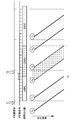

Classifications
-
- H—ELECTRICITY
- H04—ELECTRIC COMMUNICATION TECHNIQUE
- H04N—PICTORIAL COMMUNICATION, e.g. TELEVISION
- H04N25/00—Circuitry of solid-state image sensors [SSIS]; Control thereof
- H04N25/40—Extracting pixel data from image sensors by controlling scanning circuits, e.g. by modifying the number of pixels sampled or to be sampled
- H04N25/46—Extracting pixel data from image sensors by controlling scanning circuits, e.g. by modifying the number of pixels sampled or to be sampled by combining or binning pixels
-
- H—ELECTRICITY
- H04—ELECTRIC COMMUNICATION TECHNIQUE
- H04N—PICTORIAL COMMUNICATION, e.g. TELEVISION
- H04N25/00—Circuitry of solid-state image sensors [SSIS]; Control thereof
- H04N25/40—Extracting pixel data from image sensors by controlling scanning circuits, e.g. by modifying the number of pixels sampled or to be sampled
- H04N25/44—Extracting pixel data from image sensors by controlling scanning circuits, e.g. by modifying the number of pixels sampled or to be sampled by partially reading an SSIS array
- H04N25/441—Extracting pixel data from image sensors by controlling scanning circuits, e.g. by modifying the number of pixels sampled or to be sampled by partially reading an SSIS array by reading contiguous pixels from selected rows or columns of the array, e.g. interlaced scanning
-
- H—ELECTRICITY
- H04—ELECTRIC COMMUNICATION TECHNIQUE
- H04N—PICTORIAL COMMUNICATION, e.g. TELEVISION
- H04N23/00—Cameras or camera modules comprising electronic image sensors; Control thereof
- H04N23/60—Control of cameras or camera modules
-
- H—ELECTRICITY
- H04—ELECTRIC COMMUNICATION TECHNIQUE
- H04N—PICTORIAL COMMUNICATION, e.g. TELEVISION
- H04N25/00—Circuitry of solid-state image sensors [SSIS]; Control thereof
- H04N25/40—Extracting pixel data from image sensors by controlling scanning circuits, e.g. by modifying the number of pixels sampled or to be sampled
- H04N25/42—Extracting pixel data from image sensors by controlling scanning circuits, e.g. by modifying the number of pixels sampled or to be sampled by switching between different modes of operation using different resolutions or aspect ratios, e.g. switching between interlaced and non-interlaced mode
-
- H—ELECTRICITY
- H04—ELECTRIC COMMUNICATION TECHNIQUE
- H04N—PICTORIAL COMMUNICATION, e.g. TELEVISION
- H04N25/00—Circuitry of solid-state image sensors [SSIS]; Control thereof
- H04N25/70—SSIS architectures; Circuits associated therewith
- H04N25/76—Addressed sensors, e.g. MOS or CMOS sensors
- H04N25/78—Readout circuits for addressed sensors, e.g. output amplifiers or A/D converters
-
- H—ELECTRICITY
- H04—ELECTRIC COMMUNICATION TECHNIQUE
- H04N—PICTORIAL COMMUNICATION, e.g. TELEVISION
- H04N25/00—Circuitry of solid-state image sensors [SSIS]; Control thereof
- H04N25/70—SSIS architectures; Circuits associated therewith
- H04N25/79—Arrangements of circuitry being divided between different or multiple substrates, chips or circuit boards, e.g. stacked image sensors
Definitions
- the present disclosure relates to an image processing device, an image processing method, and an image processing system.
- Imaging devices are roughly classified into charge transfer type imaging devices typified by a CCD (Charge Coupled Device) image sensor and MOS type imaging devices typified by a CMOS (Complementary Metal Oxide Semiconductor) image sensor.
- CCD Charge Coupled Device
- MOS type imaging devices typified by a CMOS (Complementary Metal Oxide Semiconductor) image sensor.
- CMOS image sensor is mounted and used in mobile products such as a mobile phone including a smartphone and a camera.
- Patent Document 1 discloses a technique related to image processing provided with a plurality of ADCs that read signals from each pixel and convert the read pixel signals from an analog format to a digital format.
- ADC Analog-to-Digital Converter
- the power consumption is large, and the technology that uses ADC that converts the pixel signal of each pixel read out at high speed and high resolution reduces the power consumption by reducing the speed and resolution.
- the operation time is maximized by switching the operation from the shutter operation to the ADC that performs pixel signal conversion according to the use case. Realizes high speed and high image quality.
- Patent Document 2 discloses a method of correcting a storage time and outputting a signal when the storage time in one frame is not constant. Further, in Patent Document 3, a shutter operation and a read operation are performed, and in the process of converting the read pixel signal by the ADC, the horizontal synchronization signal is partially thinned to align the inclination of the shutter operation and the read operation. A technique is disclosed.
- a selection unit that selects the number of used ADCs that is the number of ADCs to be used among a plurality of ADCs, and a product of the number of used ADCs and the decimation rate is kept constant, and the number of used ADCs and An image processing apparatus is provided in which the thinning rate is switched.
- a shutter operation for sweeping away the accumulated pixel signals and a read operation for reading the pixel signals are performed for each frame of the captured image, and before the shutter operation is performed, the number of used ADCs and A first register and a second register which are parameter information used in the first ADC mode and the second ADC mode having different decimation rates may be set.
- the first register and the second register are set before a vertical synchronization signal given before the shutter operation that is a target of switching between the first ADC mode and the second ADC mode is started. May be.
- the processor converts the pixel signal read from the image sensor from an analog format to a digital format by a plurality of ADCs, and the pixel thinning rate in reading the pixel signal from the image sensor. Selecting a used ADC number that is the number of ADCs to be used among the plurality of ADCs, and maintaining the product of the used ADC number and the thinning-out rate in a constant state. An image processing method is provided in which the number and the thinning rate are switched.
- the computer further includes an ADC unit including a plurality of ADCs that convert a pixel signal read from the image sensor from an analog format to a digital format, and pixel thinning in reading the pixel signal from the image sensor.
- a selection unit that selects the number of ADCs to be used among the plurality of ADCs based on the rate, and a product of the number of ADCs to be used and the thinning rate is constant.
- a program for switching the number of ADCs used and the thinning rate is provided.
- the power consumption changes according to the change in the number of ADCs to be used while keeping the slopes of the shutter operation and the reading operation constant. Therefore, power consumption can be suppressed.
- FIG. 1 is a block diagram illustrating a configuration of an imaging apparatus according to an embodiment of the present disclosure. It is a figure which shows arrangement
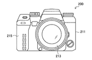
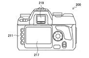
- FIGS. 1A and 1B are diagrams illustrating a digital camera to which the technology of the present disclosure is applied.
- the digital camera 200 is observed by a user at the time of photographing, a main body (camera body) 211, an interchangeable lens unit 213, a grip portion 215 held by the user at the time of photographing, a monitor portion 217 for displaying various information.
- EVF Electronic View Finder
- 1A is an external view of the digital camera 200 viewed from the front (that is, the subject side)
- FIG. 1B is an external view of the digital camera 200 viewed from the back (that is, the photographer side).
- the technique of the present disclosure can be used when, for example, the digital camera 200 captures an image and the captured image displayed on the monitor unit 217 can be prevented from being interrupted.
- CMOS image sensor (1.2. CMOS image sensor) First, the mechanism of a CMOS image sensor mounted on an imaging apparatus such as the digital camera 200 will be described.
- the image sensor is provided with a plurality of pixels.
- the electric charge accumulated in each pixel is read, and the read pixel signals are converted from an analog format to a digital format by a plurality of ADCs.
- Digital pixel signals output from the plurality of ADCs are formed as captured images by performing image processing.
- the captured image obtained here is displayed on the monitor unit 217 of the digital camera 200, for example, so that the user can confirm the captured image.
- a shutter operation for sweeping out the electric charge accumulated in each pixel which is a photoelectric conversion element and a reading operation for reading out a pixel signal accumulated in each pixel are performed.
- the time from the shutter operation to the readout operation is the time for which charges are accumulated in the pixel, and this time is called accumulation time.
- the pixel signal read from the image sensor is converted from an analog format to a digital format by a plurality of ADCs, and a digital format pixel signal is output for image processing.
- FIG. 2 is a diagram illustrating a timing chart in which the shutter operation S and the read operation R of the image sensor according to the comparative example of the technology of the present disclosure are performed.
- the interval of the horizontal synchronization signal is a signal related to the horizontal operation that is output at a predetermined interval.
- the vertical synchronization signal is a signal related to a vertical operation that is output at a predetermined interval.
- drive A and drive B two states in which the shutter operation and the reading operation are different in speed are referred to as drive A and drive B.
- drive A the interval of horizontal synchronization signals is narrower than that of drive B, and in drive B, the interval of horizontal synchronization signals is wider than that of drive A. That is, the time required to read out the pixel signals for one frame is shorter for drive A and longer for drive B.
- the shutter operation S 1 and the read operation R 1 corresponds to the drive A, until completion of the operation start, is kept constant intervals have the same inclination.
- the accumulation time of each pixel is the same up to the read operation R 1 from the shutter operation S 1 the inclination of the shutter operation and the read operation in this manner keeps a certain distance in the same It shows that there is.
- the vertical synchronizing signal at predetermined intervals is output, a timing C 1 of the drive is switched.
- the drive A is switched to the drive B.
- the reading operation R 2 reads the pixel signal at the reading speed of the driving B.
- the shutter operation S 2 corresponding to the read operation R 2 during the shutter operation S 2, are switched to the drive B from the drive A. Therefore, the inclination of the shutter operation S 2 has varied from the start to the end of the shutter operation.
- the accumulation time from the shutter operation to the reading operation is not constant throughout one frame. In this way, a frame whose accumulation time is not constant is an invalid frame and is a frame that is not used for displaying a captured image.
- timing C 2 the output further next vertical synchronizing signal, a timing C 2 to drive is switched.
- Timing C 2 the opportunity, I switched to driving A from the drive B.
- shutter operation S 3 Although from shutter operation start to the timing C 2 operates at a speed of the shutter operation in the drive B, the timing C2 to the machine, the drive A Operates at the shutter operating speed.
- the read operation R 3 reading starts, the read operation R 3 in the reading speed in the drive A is performed.
- the inclination of the shutter operation S 3 and the read operation R 3 may be not constant, within the image of one frame, the frame is caused accumulation time is not constant.
- a frame in which the accumulation time is not constant within one frame is an invalid frame and is a frame that is not used for displaying a captured image, as in the case of switching from driving A to driving B described above.
- the inventor has conducted earnest research on a technique that can maintain a constant inclination of the shutter operation and the readout operation even when switching between driving.
- a shutter operation and a read operation are performed, and the read pixel signal is converted from an analog format to a digital format by the ADC and output.
- the slope of the shutter operation and the readout operation is constant and the ADC is operated with low power consumption.
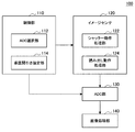
- FIG. 3 is a block diagram illustrating an example of each configuration of the imaging apparatus 100 to which the technology of the present disclosure is applied.
- the imaging apparatus 100 includes a control unit 110, an image sensor 120, an ADC unit 130, and an image processing unit 140.
- the image sensor 120 includes a shutter operation processing unit 122 and a read operation processing unit 124.
- the image sensor 120 has a function of receiving light at each pixel and reading out a pixel signal of each pixel. For example, in the image sensor 120, a plurality of pixels are arranged side by side in the horizontal direction and the vertical direction, and light of the subject for one frame of the captured image is received.
- the shutter operation processing unit 122 has a function of receiving the light of the subject in each pixel and sequentially sweeping away the accumulated charges. After the shutter operation processing unit 122 operates, charge accumulation is performed by newly receiving light of the subject in each pixel. In the shutter operation processing unit 122, a shutter operation is performed on each pixel arranged in a plurality in the horizontal direction and the vertical direction. This shutter operation starts from a pixel arranged on a horizontal line corresponding to the uppermost stage of one frame of the captured image, and is sequentially performed to the lowermost stage in the horizontal direction.
- the readout operation processing unit 124 has a function of reading out the electric charge accumulated in each pixel and outputting it to the ADC unit 130. Similar to the shutter operation, the readout operation is performed on each pixel arranged in a plurality in the horizontal direction and the vertical direction. The reading operation is started from pixels arranged on the horizontal line corresponding to the uppermost stage of one frame of the captured image, and sequentially performed to the lowermost stage in the horizontal direction.
- the ADC unit 130 has a function of converting the pixel signal read by the image sensor 120 from an analog format to a digital format and outputting the pixel signal to the image processing unit 140.
- the ADC unit includes a plurality of ADCs. The number of ADCs provided in the ADC unit 130 is not limited.
- the control unit 110 includes an ADC selection unit 112 and a vertical thinning designation unit 114.
- the control unit 110 has a function of controlling the image sensor 120 and the ADC unit 130.
- the control unit 110 may execute the above-described control by cooperation of software and hardware, for example.
- the control unit 110 may include a CPU (Central Processing Unit), a ROM (Read Only Memory), and a RAM (Random Access Memory) as hardware.
- a CPU Central Processing Unit
- ROM Read Only Memory
- RAM Random Access Memory
- the CPU functions as, for example, an arithmetic processing unit or a control unit, and controls the overall operation of each component or a part thereof based on various programs recorded in the ROM and RAM.
- the category of the technology according to the present disclosure includes a program that causes a computer including a CPU or the like to execute the functions described above, and a storage medium that stores the program.
- ROM is a means for storing programs read by the CPU, data used for calculations, and the like.
- RAM for example, a program read by the CPU, various parameters that change as appropriate when the program is executed, and the like are temporarily or permanently stored.
- the ADC selection unit 112 included in the control unit 110 has a function of selecting the number of ADCs to be used among a plurality of ADCs provided in the ADC unit 130. By selecting the number of ADCs to be used, it is possible to distinguish between ADCs that are used and ADCs that are not used. By providing an ADC that is not used, power consumption of the imaging apparatus 100 can be suppressed.
- the vertical thinning designation unit 114 has a function of designating a thinning rate for thinning pixel signals read from the image sensor in the vertical direction.
- the product of the thinning rate and the number of used ADCs is set so as to maintain a constant state. Therefore, the ADC selection unit 112 and the vertical thinning designation unit 114 cooperate to designate the thinning rate and select the number of ADCs to be used. Details of the vertical thinning will be described later.
- the vertical thinning operation means that a part of a horizontal line of pixels to be arranged is extracted and read, and the read pixel signal is converted from an analog format to a digital format using an ADC and output.
- a pixel horizontal line having a plurality of pixels in the horizontal direction pixel is an integer of 2 or more
- RGB pixel array Bayer array
- odd rows are arranged in GR rows and even rows are arranged in GB rows.
- the readout operation is sequentially performed on the n pixel horizontal lines, and when the readout operation to the nth pixel horizontal line is completed, the readout operation is performed in the vertical direction.
- the reading operation of the next row (n + 1) is performed in the horizontal direction.
- the read operation for the next frame can be sequentially performed on the pixel horizontal line of the nth row. Reading out all the rows in the vertical direction while reading out the pixel horizontal lines, converting the pixel signals, and outputting them can be called an all-pixel operation.
- the shutter operation is also sequentially performed in the same manner as the reading operation.
- the vertical thinning operation does not read out all the rows in the vertical direction, but reads out a portion of the rows arranged in the vertical direction and adds the pixel signals of the read rows.
- the pixel signal is read out as a pixel signal in an arbitrary row and the pixel signal is converted.
- a read operation is performed on two of the three rows of the GR rows arranged in odd rows, and the pixel signals are output and converted as pixel signals for one row.
- the read operation is performed on the even-numbered GB rows, and the read-out operation is performed on two rows among the three GB rows arranged in the even-numbered rows, and the pixel signals are output as one row and converted.
- the number written in the denominator indicates the thinning rate in the vertical direction. For example, in the case of a 1/6 vertical thinning operation, a read operation is performed on one of the six rows of the GR rows arranged in an odd row, and the pixel signal is converted by being output as a pixel signal for one row. Done.
- the vertical thinning operation By performing the vertical thinning operation in this way, the time required for reading and pixel signal conversion is reduced as compared with the all-pixel operation for reading all rows in the vertical direction.
- the pixel signal for one frame is read out and output to the ADC, and the time until the ADC converts the pixel signal from the analog format to the digital format is different. If this time is different, an invalid frame is generated. Therefore, it is required to make the time from the read operation to the conversion operation in the ADC constant.
- the time from reading to the conversion operation in the ADC can be changed by reducing the number of ADCs used from the number of ADCs used during all pixel operations.
- the conversion from readout to ADC is performed by specifying the vertical thinning rate (hereinafter referred to as the thinning rate) and selecting the number of ADCs to be used based on the thinning rate. It is required that the time until the operation is constant. Therefore, the generation of invalid frames can be prevented by switching the thinning rate and the number of used ADCs so that the product of the thinning rate and the number of used ADCs is constant.
- FIG. 4 is a diagram illustrating an example of the arrangement of ADCs.
- a connection unit, a plurality of ADCs, an output circuit, and a PAD are arranged on a unit substrate.
- the connection part has a pair of connection part in the center part.
- a plurality of ADCs are provided from the pair of connection portions toward both sides of the unit substrate in the direction in which the pair of connection portions are arranged.
- the plurality of ADCs include a first ADC on one side of the pair of connection portions and a second ADC on the other side, adjacent to the first ADC, adjacent to the third ADC, and adjacent to the second ADC.
- a fourth ADC is provided.
- output circuits and PADs are arranged at both ends of the unit substrate in a direction orthogonal to the direction in which the pair of connection parts are arranged.
- the ADC arrangement example shown in FIG. 4 shows a state where 12 ADCs are arranged on the unit substrate.
- an arrangement example in which a plurality of ADCs are twelve is shown, but the number of ADCs is not limited as long as it is two or more. Specifically, 2, 4, 8, 12, 16 ADCs may be arranged.
- an ADC to be used is selected from a plurality of ADCs based on the thinning rate.
- FIG. 4 shows the case where the number of ADCs to be used is 12 and the number of ADCs to be used is 2 among 12 ADCs.
- An unhatched ADC indicates an ADC that is selected as a use ADC, and a hatched ADC indicates an ADC that is not used. For example, in FIG. 4, when the number of ADCs to be used is two, the first ADC and the second ADC that are closest to the pair of connection portions are selected.
- pixels are not described, but the pixels may be provided on a unit substrate on which a plurality of ADCs are provided, or pixels are separately provided on a wafer. It may be laminated on the unit substrate. By separately providing pixels on the wafer, an increase in cost due to an increase in chips can be suppressed.
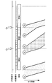
- FIG. 5 is a timing chart when the number of ADCs used is switched between 12 and 2.
- the relationship between the number of used ADCs and the thinning rate shown in FIG. 5 is that when the operation is performed at a thinning rate of 1/6, the number of used ADCs is 2, and when the operation is performed at a thinning rate of 1/1, the number of used ADCs. There are twelve.
- the slopes of the shutter operations s 1, s 2, and s 3 and the read-out operations r 1, r 2, and r 3 are made constant by changing the thinning rate and the number of ADCs to be used. That is, the slopes of the shutter operation s 1 and the readout operation r 1 and the shutter operation s 2 and the readout operation r 2 are constant. This is because the number of ADCs to be used is switched from 2 to 12 at timing e 1 when the thinning rate is switched from 1/6 to 1/1. In this manner, by switching the thinning rate and the number of ADCs to be used, power consumption can be suppressed throughout the entire frame, and the slopes of the shutter operation and the readout operation are constant.
- FIG. 5 is a diagram in which a description related to the setting for switching between the first ADC mode and the second ADC mode is added to FIG. 5.
- the vertical thinning is 1/6 vertical thinning in the first ADC mode
- the second ADC mode is 1/1 vertical thinning.
- the number of ADCs to be used is two, and in the second ADC mode, the number of ADCs to be used is twelve.
- the shutter operation s 1 corresponding to a period from a vertical synchronizing signal v 1 to a vertical synchronizing signal v 2 is performed from before the vertical synchronizing signal v 1, the vertical synchronizing signal v 1 the timing, shutter operation s 1 is ongoing.
- the read operation r 1 is performed after the vertical synchronization signal v 1 and sequentially starts after a predetermined accumulation time is completed from the shutter operation s 1 .
- the shutter operation s 2 and the readout operation r 2 correspond to the period from the next vertical synchronization signal v 2 to the vertical synchronization signal v 3 , and the shutter operation s 2 is performed before the vertical synchronization signal v 2. at the timing of the vertical synchronizing signal v 2, shuttering s 2 are ongoing.
- Read operation r 2 is performed after the vertical synchronizing signal v 2, after the lapse of the shutter operation s 2 a predetermined accumulation time is sequentially started.
- the number of ADC to be used is switched. Referring to FIG. 6, the number of ADCs used during the shutter operation s 2 is switched from 2 to 12.
- the shutter operation s 2 is performed in the second ADC mode over the previous period and the subsequent period of the vertical synchronization signal v 2 . Therefore, the inclination of the shutter operation s 2 is maintained constant. Since the shutter operation s 2 operates in the second ADC mode even in the previous period of the vertical synchronization signal v 2 , the technique of the present disclosure is used for the first ADC mode at the time of the vertical synchronization signal v 1. In addition to the first register that is parameter information, it is desirable to set a second register that is parameter information used in the second ADC mode.
- the number of ADCs used during the shutter operation s 3 is switched from 12 to 2.
- the shutter operation s 3 are over the previous period and the rear periods of the vertical synchronizing signal v 3, takes place in the second ADC mode. Therefore, the inclination of the shutter operation s 3 is maintained constant. Since the shutter operation s 3 operates in the first ADC mode even in the previous period of the vertical synchronization signal v 3 , the technique of the present disclosure is used for the second ADC mode at the time of the vertical synchronization signal v 2. In addition to the second register that is parameter information, it is desirable to set the first register that is parameter information used in the first ADC mode.
- the first register which is parameter information used in the first ADC mode is set.
- the first register is preferably set between the vertical synchronizing signal v 3 a switch to the first ADC mode is outputted after switching and timing e 2 made.
- the power consumption is reduced when the number of ADCs to be used decreases while the slope of the shutter operation and the readout operation is kept constant.
- Generation of invalid frames can be prevented while suppressing consumption.
- the imaging device is built in the digital camera, but the present technology is not limited to such an example.
- the present invention may be applied to smartphones and other electronic devices.
Landscapes
- Engineering & Computer Science (AREA)
- Multimedia (AREA)
- Signal Processing (AREA)
- Transforming Light Signals Into Electric Signals (AREA)
- Studio Devices (AREA)
Abstract
【課題】電力の消費を抑制しつつ、無効フレームの発生を防止する。 【解決手段】イメージセンサから読み出される画素信号をアナログ形式からデジタル形式に変換する複数のADCを備えるADC部と、前記イメージセンサからの前記画素信号の読出しにおける画素の間引き率に基づき、前記複数のADCのうちで使用するADCの数である使用ADC数を選択する選択部と、を含み、前記使用ADC数と前記間引き率との積が一定の状態を保って、前記使用ADC数及び前記間引き率が切り替わる、画像処理装置。
Description
本開示は、画像処理装置、画像処理方法及び画像処理システムに関する。
近年では、様々な種類の撮像装置が開発されている。撮像装置は、CCD(Charge Coupled Device)イメージセンサに代表される電荷転送型撮像装置と、CMOS(Complementary Metal Oxide Semiconductor)イメージセンサに代表されるMOS型撮像装置に大別される。そして、例えばCMOSイメージセンサは特に、スマートフォンを含む携帯電話、カメラ等のモバイル製品に搭載されて用いられている。
CMOSイメージセンサにおいては、ユーザの様々なユースケースに応じて、シャッター動作及び読み出し動作により読み出された各画素の信号をアナログ形式からデジタル形式に変換するADC(Analog-to-Digital Converter)の切り替え動作が行われる。特許文献1には、各画素から信号を読み出して、読み出した画素信号をアナログ形式からデジタル形式へ変換するADCが複数設けられた画像処理に関する技術が開示されている。例えば、CMOSイメージセンサの中には、消費電力が大きく、高速かつ高解像で読み出された各画素の画素信号を変換するADCを使用する技術、速度及び解像度を低下させて消費電力を低下して読み出された画素信号を変換するADCを使用する技術等がある。複数のADCを使用するスマートフォンを含む携帯電話、カメラ等のモバイル製品においては、これらのシャッター動作から画素信号の変換を行うADCまで動作をユースケースに応じて切り替えることにより、動作可能時間の最大化と高速及び高画質とを実現している。
しかしながら、ADC動作の切り替え時には、イメージセンサにおけるシャッター動作の傾き及び読み出し動作の傾きを一定に保てないことにより、各画素におけるシャッター動作から読出し動作開始までの画素による電荷の蓄積時間が、1つの撮像画像を形成する1フレーム内で一定ではなくなっていた。蓄積時間が一定ではないフレームは、無効フレームとされ、表示には使用されなかった。
このような無効フレームを発生させないように様々な技術が開発されている。例えば、異なる種類のADCの間で、シャッター動作及び読出し動作の傾きは異なるが、蓄積時間に制約を設けることで、1フレーム内の蓄積時間を一定とする方法が開示されている。
また、特許文献2には、1フレーム内の蓄積時間が一定でない場合に、蓄積時間を補正して、信号を出力する手法が開示されている。さらに、特許文献3には、シャッター動作及び読み出し動作が行われ、読み出された画素信号をADCにより変換する過程で、水平同期信号を一部間引くことにより、シャッター動作及び読出し動作の傾きを揃える手法が開示されている。
しかし、上記のような技術においては、蓄積時間に制約が生じたり、新たな補正機構が必要であったり、補正が不十分である場合に1フレーム内で段差が発生してしまったりしていた。また、特許文献3に開示の技術では、蓄積時間は保障されるものの、低消費電力を実現する上で、その効果は限定的であった。
上記事情に鑑みれば、電力の消費を抑制しつつ、無効フレームの発生を防止することが望ましい。
本開示によれば、イメージセンサから読み出される画素信号をアナログ形式からデジタル形式に変換する複数のADCを備えるADC部と、前記イメージセンサからの前記画素信号の読出しにおける画素の間引き率に基づき、前記複数のADCのうちで使用するADCの数である使用ADC数を選択する選択部と、を含み、前記使用ADC数と前記間引き率との積が一定の状態を保って、前記使用ADC数及び前記間引き率が切り替わる、画像処理装置が提供される。
前記イメージセンサでは、蓄積された画素信号を掃き捨てるシャッター動作と、前記画素信号を読み出す読み出し動作とが、撮像画像1フレーム毎に行われ、前記シャッター動作が行われる前に、前記使用ADC数及び前記間引き率が異なる第1のADCモード及び第2のADCモードに利用されるパラメータ情報である第1のレジスタ及び第2のレジスタが設定されてもよい。
前記第1のレジスタ及び前記第2のレジスタは、前記第1のADCモード及び前記第2のADCモードが切り替わる対象となる前記シャッター動作が開始する前に与えられた垂直同期信号よりも前に設定されてもよい。
また、本開示によれば、プロセッサが、イメージセンサから読み出される画素信号を複数のADCによりアナログ形式からデジタル形式に変換することと、前記イメージセンサからの前記画素信号の読出しにおける画素の間引き率に基づき、前記複数のADCのうちで使用するADCの数である使用ADC数を選択することと、を含み、前記使用ADC数と前記間引き率との積が一定の状態を保って、前記使用ADC数及び前記間引き率が切り替わる、画像処理方法が提供される。
また、本開示によれば、コンピュータを、イメージセンサから読み出される画素信号をアナログ形式からデジタル形式に変換する複数のADCを備えるADC部と、前記イメージセンサからの前記画素信号の読出しにおける画素の間引き率に基づき、前記複数のADCのうちで使用するADCの数である使用ADC数を選択する選択部と、として機能させ、さらに、前記使用ADC数と前記間引き率との積が一定の状態を保って、前記使用ADC数及び前記間引き率が切り替わるためのプログラムが提供される。
本開示によれば、使用するADC数と間引き率との積を一定とすることで、シャッター動作及び読み出し動作の傾きを一定としたまま、使用するADC数の変化に応じて消費電力が変化するため、電力の消費を抑制できる。
以上説明したように本開示によれば、電力の消費を抑制しつつ、無効フレームの発生を防止できる。
なお、上記の効果は必ずしも限定的なものではなく、上記の効果とともに、または上記の効果に代えて、本明細書に示されたいずれかの効果、または本明細書から把握され得る他の効果が奏されてもよい。
なお、上記の効果は必ずしも限定的なものではなく、上記の効果とともに、または上記の効果に代えて、本明細書に示されたいずれかの効果、または本明細書から把握され得る他の効果が奏されてもよい。
以下に添付図面を参照しながら、本開示の好適な実施の形態について詳細に説明する。なお、本明細書及び図面において、実質的に同一の機能構成を有する構成要素については、同一の符号を付することにより重複説明を省略する。
なお、説明は以下の順序で行うものとする。
1. 本開示の技術概要
1.1. 本開示の技術が適用され得る電子機器の一例
1.2. CMOSイメージセンサ
1.3. 本開示の技術に想到する背景
2. 本開示の技術が適用され得る撮像装置に関して
2.1. 機能及び構成
2.2. 垂直間引き率及び使用ADC数の関係
2.3. ADCの配置例
2.4. 動作流れ
1. 本開示の技術概要
1.1. 本開示の技術が適用され得る電子機器の一例
1.2. CMOSイメージセンサ
1.3. 本開示の技術に想到する背景
2. 本開示の技術が適用され得る撮像装置に関して
2.1. 機能及び構成
2.2. 垂直間引き率及び使用ADC数の関係
2.3. ADCの配置例
2.4. 動作流れ
(1.本開示の技術概要)
(1.1.本開示の技術が適用され得る電子機器の一例)
図1A及び図1Bを参照して、本開示の技術が適用される電子機器の一例を説明する。図1Aおよび図1Bは、本開示の技術が適用されたデジタルカメラを示した図である。デジタルカメラ200は、本体部(カメラボディ)211と、交換式のレンズユニット213と、撮影時にユーザによって把持されるグリップ部215と、各種情報を表示するモニタ部217と、撮影時にユーザによって観察されるスルー画を表示するEVF(Electronic View Finder)219と、を備える。なお、図1Aは、デジタルカメラ200を前方(すなわち、被写体側)から眺めた外観図であり、図1Bは、デジタルカメラ200を後方(すなわち、撮影者側)から眺めた外観図である。
(1.1.本開示の技術が適用され得る電子機器の一例)
図1A及び図1Bを参照して、本開示の技術が適用される電子機器の一例を説明する。図1Aおよび図1Bは、本開示の技術が適用されたデジタルカメラを示した図である。デジタルカメラ200は、本体部(カメラボディ)211と、交換式のレンズユニット213と、撮影時にユーザによって把持されるグリップ部215と、各種情報を表示するモニタ部217と、撮影時にユーザによって観察されるスルー画を表示するEVF(Electronic View Finder)219と、を備える。なお、図1Aは、デジタルカメラ200を前方(すなわち、被写体側)から眺めた外観図であり、図1Bは、デジタルカメラ200を後方(すなわち、撮影者側)から眺めた外観図である。
本開示の技術は、例えば、デジタルカメラ200において、撮像する際に使用され、モニタ部217にて表示される撮像画像が途切れることを防止できる。
(1.2.CMOSイメージセンサ)
まず、デジタルカメラ200のような撮像装置に搭載されるCMOSイメージセンサの機構に関して説明を行う。イメージセンサには、複数の画素が設けられている。イメージセンサでは、各画素に蓄積された電荷を読み出して、複数のADCで、読み出された画素信号をアナログ形式からデジタル形式に変換する。この複数のADCから出力されたデジタル形式の画素信号は、画像処理が施されることで撮像画像として形成される。ここで得られた撮像画像はデジタルカメラ200のモニタ部217にて、例えば表示されることで、ユーザが撮像画像を確認することができる。
まず、デジタルカメラ200のような撮像装置に搭載されるCMOSイメージセンサの機構に関して説明を行う。イメージセンサには、複数の画素が設けられている。イメージセンサでは、各画素に蓄積された電荷を読み出して、複数のADCで、読み出された画素信号をアナログ形式からデジタル形式に変換する。この複数のADCから出力されたデジタル形式の画素信号は、画像処理が施されることで撮像画像として形成される。ここで得られた撮像画像はデジタルカメラ200のモニタ部217にて、例えば表示されることで、ユーザが撮像画像を確認することができる。
イメージセンサ内では、具体的に、光電変換素子である各画素に蓄積されている電荷を掃き捨てるシャッター動作と、各画素に蓄積された画素信号を読み出す読出し動作が行われる。このシャッター動作から読み出し動作までが画素に電荷が蓄積される時間であり、この時間を蓄積時間と称す。その後、イメージセンサから読み出された画素信号は、複数のADCにより、アナログ形式からデジタル形式に変換され、デジタル形式の画素信号が出力されて、画像処理が行われる。
(1.3.本開示の技術に想到する背景)
本開示の技術背景に関して、図2を参照して説明を行う。図2は、本開示の技術の比較例にかかるイメージセンサのシャッター動作S及び読み出し動作Rが行われるタイミングチャートを示した図である。水平同期信号の間隔は、所定の間隔で出力される水平方向の動作に関する信号である。垂直同期信号は、所定の間隔で出力される垂直方向の動作に関する信号である。
本開示の技術背景に関して、図2を参照して説明を行う。図2は、本開示の技術の比較例にかかるイメージセンサのシャッター動作S及び読み出し動作Rが行われるタイミングチャートを示した図である。水平同期信号の間隔は、所定の間隔で出力される水平方向の動作に関する信号である。垂直同期信号は、所定の間隔で出力される垂直方向の動作に関する信号である。
例えば、シャッター動作及び読み出し動作の速度が異なる2つの状態を駆動A及び駆動Bとする。駆動Aでは、水平同期信号の間隔が駆動Bより狭く、駆動Bでは、水平同期信号の間隔が駆動Aよりも広い。つまり、1フレーム分の画素信号を読み出す際にかかる時間は、駆動Aの方が短く、駆動Bの方が長い。そして、駆動Aに対応するシャッター動作S1及び読み出し動作R1は、動作開始から終了まで、同一の傾きを有し一定の間隔を保っている。この様にシャッター動作及び読み出し動作の傾きが同一で一定の間隔を保つことは、画素配列の全ての水平ラインにおいて、シャッター動作S1からの読み出し動作R1までで各画素の蓄積時間が同じであることを示している。
図2では、所定の間隔で垂直同期信号が出力され、駆動が切り替わるタイミングC1を示している。タイミングC1を機に、駆動Aが駆動Bに切り替わる。例えば、このようにタイミングC1で駆動Aから駆動Bに切り替わると、読み出し動作R2は駆動Bの読み出し速度にて画素信号を読み出す。一方で、読み出し動作R2に対応するシャッター動作S2では、シャッター動作S2の途中で、駆動Aから駆動Bに切り替わっている。そのため、シャッター動作S2の傾きが、シャッター動作の開始から終了までで変化している。
つまり、タイミングC1の前後でシャッター動作S2が継続して行われており、タイミングC1で駆動Aから駆動Bに切り替わると、シャッター動作S2は、駆動Aにおけるシャッター動作の速度から、駆動Bにおけるシャッター動作の速度に変化する。よってシャッター動作から読み出し動作までの蓄積時間が、1フレームを通して一定ではなくなる。このように、蓄積時間が一定でないフレームは、無効フレームとされ、撮像画像の表示には使用されないフレームとなる。
次に、図2では、さらに次の垂直同期信号が出力され、駆動が切り替わるタイミングC2を示している。タイミングC2を機に、駆動Bから駆動Aに切り替わる。例えば、タイミングC2の前後ではシャッター動作S3が継続して行われている。タイミングC2で駆動Bから駆動Aに切り替わると、シャッター動作S3は、シャッター動作開始からタイミングC2までは駆動Bにおけるシャッター動作の速度にて動作するものの、タイミングC2を機に、駆動Aにおけるシャッター動作速度にて動作する。
一方で、タイミングC2で駆動Bから駆動Aに切り替わった後に、読み出しが始まる読み出し動作R3では、駆動Aにおける読み出し速度で読み出し動作R3が行われる。これより、シャッター動作S3及び読み出し動作R3の傾きは一定ではなくなり、1フレームの画像内で、蓄積時間が一定でないフレームが生じる。このように1フレーム内で蓄積時間が一定でないフレームは、上述した駆動Aから駆動Bに切り替わった時と同様に、無効フレームとされ、撮像画像の表示には使用されないフレームとなる。
そこで、発明者は、駆動間の切り替えを行っても、シャッター動作及び読み出し動作の傾きが一定とできる技術に関して、鋭意研究を行った。各駆動内では、シャッター動作及び読み出し動作が行われ、読み出された画素信号は、ADCにてアナログ形式からデジタル形式へ変換されて出力される。これより、ADCに着目してシャッター動作及び読み出し動作の傾きが一定であり、かつ低消費電力にてADCを動作させる技術を想到した。
(2.本開示の技術が適用され得る撮像装置に関して)
(2.1.機能及び構成)
図3を参照して、本開示の技術を適用した撮像装置100の機能及び構成を説明する。図3は、本開示の技術を適用した撮像装置100の各構成の一例をブロック図にて示した図である。撮像装置100は、制御部110、イメージセンサ120、ADC部130、及び画像処理部140を含む。
(2.1.機能及び構成)
図3を参照して、本開示の技術を適用した撮像装置100の機能及び構成を説明する。図3は、本開示の技術を適用した撮像装置100の各構成の一例をブロック図にて示した図である。撮像装置100は、制御部110、イメージセンサ120、ADC部130、及び画像処理部140を含む。
((イメージセンサ))
イメージセンサ120は、シャッター動作処理部122及び読み出し動作処理部124を含む。イメージセンサ120は、各画素にて受光を行い、各画素の画素信号の読み出しを行う機能を有する。例えば、イメージセンサ120では、水平方向及び垂直方向に複数の画素が並んで配置され、撮像画像1フレーム分の被写体の光を受光する。
イメージセンサ120は、シャッター動作処理部122及び読み出し動作処理部124を含む。イメージセンサ120は、各画素にて受光を行い、各画素の画素信号の読み出しを行う機能を有する。例えば、イメージセンサ120では、水平方向及び垂直方向に複数の画素が並んで配置され、撮像画像1フレーム分の被写体の光を受光する。
シャッター動作処理部122は、各画素において被写体の光を受光して蓄積された電荷を順次掃き捨てる機能を有する。シャッター動作処理部122が動作した後には、各画素において、新たに被写体の光の受光が行われることで電荷の蓄積が行われる。シャッター動作処理部122では、水平方向及び垂直方向に複数並んで配置される各画素に対して、シャッター動作が行われる。このシャッター動作は、撮像画像1フレームの最上段に対応する水平ラインに配置される画素から開始され、水平方向最下段まで順次行われる。
読み出し動作処理部124は、各画素において蓄積された電荷を読み出して、ADC部130に出力する機能を有する。読み出し動作は、シャッター動作と同様に、水平方向及び垂直方向に複数並んで配置される各画素に対して行われる。読み出し動作は、撮像画像1フレームの最上段に対応する水平ラインに配置される画素から開始され、水平方向最下段まで順次行われる。
((ADC部))
ADC部130は、イメージセンサ120にて読み出された画素信号をアナログ形式からデジタル形式に変換して、画素信号を画像処理部140に出力する機能を有する。ADC部は、複数のADCを備えている。ADC部130に備えられるADCの数は限定されない。
ADC部130は、イメージセンサ120にて読み出された画素信号をアナログ形式からデジタル形式に変換して、画素信号を画像処理部140に出力する機能を有する。ADC部は、複数のADCを備えている。ADC部130に備えられるADCの数は限定されない。
((制御部110))
制御部110は、ADC選択部112及び垂直間引き指定部114を含む。制御部110は、イメージセンサ120及びADC部130を制御する機能を有する。
制御部110は、ADC選択部112及び垂直間引き指定部114を含む。制御部110は、イメージセンサ120及びADC部130を制御する機能を有する。
制御部110は、例えば、ソフトウェアとハードウェアとの協働によって上述した制御を実行してもよい。例えば、制御部110は、ハードウェアとして、CPU(Central Processing Unit)と、ROM(Read Only Memory)と、RAM(Random Access Memory)と、を備えてもよい。
CPUは、例えば、演算処理装置または制御装置として機能し、ROM、RAMに記録された各種プログラムに基づいて各構成要素の動作全般またはその一部を制御する。なお、本開示に係る技術の範疇には、CPU等を含むコンピュータに上述した機能を実行させるプログラム、及び該プログラムを記憶させた記憶媒体も含まれるとする。
ROMは、CPUに読み込まれるプログラムや演算に用いるデータ等を格納する手段である。RAMには、例えば、CPUに読み込まれるプログラムや、そのプログラムを実行する際に適宜変化する各種パラメータ等が一時的または永続的に格納される。
制御部110に含まれるADC選択部112は、ADC部130に備えられる複数のADCの内で、使用するACDの数を選択する機能を有する。使用するADCの数を選択することにより、使用するADCと使用しないADCを分別することができる。使用しないADCを設けることにより、撮像装置100の電力消費を抑制することができる。
垂直間引き指定部114は、イメージセンサから読み出される画素信号を垂直方向に間引く間引き率を指定する機能を有する。ここで、間引き率と使用ADC数との積は一定の状態を保つように設定される。よって、ADC選択部112及び垂直間引き指定部114は協働して、間引き率を指定したり使用するADC数を選択したりする。垂直間引きの詳しくは、後述する。
(2.2.垂直間引き率及び使用ADC数の関係)
まず、垂直間引きに関して説明する。垂直間引き動作とは、配列される画素の水平ラインの一部を抽出して読み込んで、読み込まれた画素信号はADCを用いてアナログ形式からデジタル形式に変換されて出力されることをいう。例えば、R(赤)G(緑)B(青)のカラーコーディングの色フィルタを持つ各画素において、水平方向に複数の画素(画素は2以上の整数)を有した画素水平ラインが、垂直方向にn行配置されるRGB画素配列(ベイヤ―配列)の例を用いて説明する。
まず、垂直間引きに関して説明する。垂直間引き動作とは、配列される画素の水平ラインの一部を抽出して読み込んで、読み込まれた画素信号はADCを用いてアナログ形式からデジタル形式に変換されて出力されることをいう。例えば、R(赤)G(緑)B(青)のカラーコーディングの色フィルタを持つ各画素において、水平方向に複数の画素(画素は2以上の整数)を有した画素水平ラインが、垂直方向にn行配置されるRGB画素配列(ベイヤ―配列)の例を用いて説明する。
ベイヤ―配列では、奇数行がGR行、偶数行がGB行で並んで配置されている。このベイヤ―配列に対して、例えば、画素信号の読み出し動作は、画素水平ラインn行に対して順次読み出し動作が行われ、n行目の画素水平ラインへの読み出し動作が終了すると、垂直方向に次行である(n+1)行目の読み出し動作を水平方向に行う。例えば、垂直方向の全ての行に対して、読み出し動作が行われた後は、次のフレームにかかる読み出し動作が順次n行目の画素水平ラインへ行われ得る。画素水平ラインを読み出す中で、垂直方向に全ての行を読み出して画素信号の変換を行い、出力することを、全画素動作と呼ぶことができる。シャッター動作に関しても、読み出し動作と同様に順次行われる。
一方で、垂直間引き動作とは、垂直方向の全ての行に対して読み出しを行うのではなく、垂直方向に配置される行の一部を間引いて読み出しを行い、読み出した行の画素信号を加算して、任意の行の画素信号として読み出して、画素信号の変換が行われる動作である。例えば、2/3垂直間引きであれば、奇数行に並ぶGR行の3行のうち、2行に対して読み出し動作が行われ、1行分の画素信号として出力され画素信号の変換が行われる。偶数行のGB行においても同様に、読み出し動作を行い、偶数行に並ぶGB行の3行のうち、2行に対して読み出し動作を行い、1行分の画素信号として出力され画素信号の変換が行われる。分母に表記される数字が、垂直方向の間引き率を示す。例えば、1/6垂直間引き動作であれば、奇数行に並ぶGR行の6行のうち、1行に対して読み出し動作が行われ、1行分の画素信号として出力されて画素信号の変換が行われる。このように垂直間引き動作を行うことで、垂直方向に全ての行を読み出す全画素動作に比べて、読み出し及び画素信号の変換にかかる時間は低減される。
しかしながら、このように全画素動作と垂直間引き動作では、1フレーム分の画素信号を読み出してADCへ出力し、ADCが画素信号をアナログ形式からデジタル形式へ変換するまでの時間が異なる。この時間が異なれば、無効フレームが発生してしまうため、読み出し動作からADCにおける変換動作までの時間を一定とすることが求められる。
よって、垂直間引き動作を行う際には、使用するADC数を全画素動作時に使用するADC数から減少させることで、読み出しからADCにおける変換動作までの時間を変化させることができる。シャッター動作及び読み出し動作の傾きを一定とするには、垂直間引き率(以下間引き率と称す。)を指定して、間引き率に基づいて使用するADC数を選択することで、読み出しからADCにおける変換動作までの時間を一定とすることが求められる。よって、間引き率と使用ADC数との積が一定となるように、間引き率と使用ADC数が切り替わることで、無効フレームの発生を防止することができる。
(2.3.ADCの配置例)
ここで、図4を参照して、ADCの配置例の説明を行う。図4は、ADCの配置例の一例を示した図である。図4では、単位基板上に、接続部、複数のADC、出力回路及びPADが配置されている。接続部は、中心部に一対の接続部を有している。一対の接続部が配置される方向において、一対の接続部から一対の接続部が配置される方向の単位基板の両側に向かって、複数のADCが備えられている。複数のADCは、一対の接続部の片側に第1のADC、もう片側に第2のADCを備え、第1のADCには隣り合って第3のADC、第2のADCには隣り合って第4のADCが備えられている。また、一対の接続部が配置される方向と直交する方向には、単位基板の両端部に出力回路およびPADが配置されている。
ここで、図4を参照して、ADCの配置例の説明を行う。図4は、ADCの配置例の一例を示した図である。図4では、単位基板上に、接続部、複数のADC、出力回路及びPADが配置されている。接続部は、中心部に一対の接続部を有している。一対の接続部が配置される方向において、一対の接続部から一対の接続部が配置される方向の単位基板の両側に向かって、複数のADCが備えられている。複数のADCは、一対の接続部の片側に第1のADC、もう片側に第2のADCを備え、第1のADCには隣り合って第3のADC、第2のADCには隣り合って第4のADCが備えられている。また、一対の接続部が配置される方向と直交する方向には、単位基板の両端部に出力回路およびPADが配置されている。
図4に記載されるADC配置例では、12個のADCが単位基板上に配置される様子を示している。かかる例では、複数のADCが12個である配置例を示しているが、ADCの個数は、2以上であれば限定されない。具体的には、2、4、8、12、16個のADCが配置されていてもよい。
本開示の技術では、間引き率に基づいて、複数設けられたADCのうち使用するADCを選択する。図4では、12個配置されるADCの内、使用するADC数が12個の場合、及び使用するADC数が2個とした場合を示している。ハッチングされていないADCが使用ADCとして選択されたADCを示しており、ハッチングされたADCは、使用されないADCを示している。例えば、図4においては、使用するADC数が2個の場合には、一対の接続部に最も近い、第1のADC及び第2のADCが選択されている。
なお、図4に記載されるADC配置例では、画素の記載がされていないが、画素は複数のADCが設けられる単位基板上に画素が設けられてもよく、別途ウエハ上に画素が設けられ単位基板に積層化されてもよい。別途ウエハ上に画素が設けられることにより、チップの増大によるコスト増加等を抑制することができる。
(2.4.動作流れ)
次に、図5及び図6を参照して、使用されるADC数が12個から2個の間で切り替わる動作に関して説明を行う。図5は、使用されるADC数が12個から2個の間で切り替わる場合のタイミングチャートを示す図である。図5に示す使用ADC数及び間引き率の関係は、間引き率が1/6で動作を行う時には、使用ADC数は2個であり、間引き率が1/1で動作を行う時には、使用ADC数が12個である。
次に、図5及び図6を参照して、使用されるADC数が12個から2個の間で切り替わる動作に関して説明を行う。図5は、使用されるADC数が12個から2個の間で切り替わる場合のタイミングチャートを示す図である。図5に示す使用ADC数及び間引き率の関係は、間引き率が1/6で動作を行う時には、使用ADC数は2個であり、間引き率が1/1で動作を行う時には、使用ADC数が12個である。
図5において、間引き率及び使用するADC数が変更されることにより、シャッター動作s1、s2、s3及び読み止し動作r1、r2、r3の傾きが一定となっている。つまり、シャッター動作s1及び読み出し動作r1と、シャッター動作s2及び読み出し動作r2との傾きが一定である。これは、間引き率が1/6から間引き率が1/1で切り替えられる際に、使用するADCの数をタイミングe1にて2個から12個に切り替えることによる。このように、間引き率及び使用するADC数を切り替えることにより、全フレームを通して、電力消費を抑制することができる上、シャッター動作及び読み出し動作の傾きが一定となる。
図5に示すように、使用するADC数は、1フレームのシャッター動作が行われている間に切り替わる。この切り替えに関して、図6を参照して、シャッター動作中に使用するADC数を異ならせる場合を第1のADCモード及び第2のADCモードとして説明を行う。図6は、図5に対して、第1のADCモード及び第2のADCモードが切り替わる設定に関する記載を追加した図である。ここで、図5と同様に、垂直間引きは、第1のADCモードでは、1/6垂直間引きであり、第2のADCモードは、1/1垂直間引きである。また、第1のADCモードでは、使用するADC数が2個であり、第2のADCモードでは、使用するADC数が12個である。
まず、図6を参照すると、垂直同期信号v1から垂直同期信号v2までの期間に対応するシャッター動作s1は、垂直同期信号v1よりも前から行われており、垂直同期信号v1のタイミングでは、シャッター動作s1は継続中である。読み出し動作r1は、垂直同期信号v1よりも後に行われ、シャッター動作s1から所定の蓄積時間が完了した後に、順次開始する。
次の垂直同期信号v2から垂直同期信号v3までの期間にはシャッター動作s2及び読み出し動作r2が対応し、シャッター動作s2は、垂直同期信号v2よりも前から行われており、垂直同期信号v2のタイミングでは、シャッター動作s2は継続中である。読み出し動作r2は、垂直同期信号v2よりも後に行われ、シャッター動作s2から所定の蓄積時間が経過した後に、順次開始する。
本開示の技術では、シャッター動作s2が動作している最中に、使用するADC数が切り替わる。図6を参照すると、シャッター動作s2の動作最中に使用するADC数が2個から12個に切り替わっている。
ここで、シャッター動作s2は、垂直同期信号v2の前期間および後期間に亘り、第2のADCモードで行われる。このため、シャッター動作s2の傾きが一定に維持される。垂直同期信号v2の前期間においてもシャッター動作s2が第2のADCモードで動作するために、本開示の技術では、垂直同期信号v1の時点では、第1のADCモードに利用されるパラメータ情報である第1のレジスタに加え、第2のADCモードに利用されるパラメータ情報である第2のレジスタが設定されることが望ましい。
例えば、図6においては、シャッター動作s2が動作している最中に、使用するADC数が2個から12個へ切り替わっている。この切り替えは、シャッター動作s2が動作を開始する前に出力された垂直同期信号v1よりも前のタイミングc1にて、第1のレジスタおよび第2のレジスタが設定されることにより実現される。これにより、撮像装置100に不具合が生じずに撮像を行うことができる。
さらに、図6を参照すると、シャッター動作s3の動作最中に使用するADC数が12個から2個に切り替わっている。
ここで、シャッター動作s3は、垂直同期信号v3の前期間および後期間に亘り、第2のADCモードで行われる。このため、シャッター動作s3の傾きが一定に維持される。垂直同期信号v3の前期間においてもシャッター動作s3が第1のADCモードで動作するために、本開示の技術では、垂直同期信号v2の時点では、第2のADCモードに利用されるパラメータ情報である第2のレジスタに加え、第1のADCモードに利用されるパラメータ情報である第1のレジスタが設定されることが望ましい。
例えば、図6においては、シャッター動作s3が動作している最中に、使用するADC数が12個から2個へ切り替わっている。この切り替えは、シャッター動作s3が動作を開始する前に出力された垂直同期信号v2よりも前のタイミングc2にて、第2のレジスタおよび第1のレジスタが設定されることにより実現される。これにより、撮像装置100に不具合が生じずに撮像を行うことができる。
上記では、所定のシャッター動作の最中に、使用するADC数が切り替わる場合に関して説明を行ったが、所定のシャッター動作の最中に使用するADC数の切り替えは行われない場合に関して説明を行う。図6を参照すると、シャッター動作s3の動作最中に第2のADCモードから第1のADCモードに切り替えが行われ、切り替え後には第1のモードが継続する場合を示している。この時、シャッター動作s3の次に行われるシャッター動作では、第1のADCモードが継続している。
この場合には、切り替え後のシャッター動作が行われる前に、第1のADCモードに利用されるパラメータ情報である第1のレジスタが設定される。図6では、例えば第1のADCモードへの切り替えが行われたタイミングe2と切り替え後に出力される垂直同期信号v3との間で第1のレジスタが設定されることが好ましい。
上記のような構成を有して、使用するADC数と間引き率との積を一定とすることで、シャッター動作及び読み出し動作の傾きを一定としたまま、使用するADC数が減少するときには電力の消費を抑えつつ、無効フレームの発生を防止できる。無効フレームを防止することにより、撮像装置における撮影連射速度の低下が抑制されたり、ユーザが撮影したい瞬間を取り逃さずに撮像体験を行ったりすることができる。
以上、添付図面を参照しながら本開示の好適な実施形態について詳細に説明したが、本開示の技術的範囲はかかる例に限定されない。本開示の技術分野における通常の知識を有する者であれば、特許請求の範囲に記載された技術的思想の範疇内において、各種の変更例または修正例に想到し得ることは明らかであり、これらについても、当然に本開示の技術的範囲に属するものと了解される。
例えば、上記実施形態では、デジタルカメラに内蔵される撮像装置としたが、本技術はかかる例に限定されない。例えば、スマートフォン、その他電子機器等に適用されてもよい。
また、本明細書に記載された効果は、あくまで説明的または例示的なものであって限定的ではない。つまり、本開示に係る技術は、上記の効果とともに、または上記の効果に代えて、本明細書の記載から当業者には明らかな他の効果を奏しうる。
100 撮像装置
110 制御部
112 ADC選択部
114 垂直間引き指定部
120 イメージセンサ
122 シャッター動作処理部
124 読み出し動作処理部
130 ADC部
140 画像処理部
110 制御部
112 ADC選択部
114 垂直間引き指定部
120 イメージセンサ
122 シャッター動作処理部
124 読み出し動作処理部
130 ADC部
140 画像処理部
Claims (5)
- イメージセンサから読み出される画素信号をアナログ形式からデジタル形式に変換する複数のADCを備えるADC部と、
前記イメージセンサからの前記画素信号の読出しにおける画素の間引き率に基づき、前記複数のADCのうちで使用するADCの数である使用ADC数を選択する選択部と、を含み、
前記使用ADC数と前記間引き率との積が一定の状態を保って、前記使用ADC数及び前記間引き率が切り替わる、画像処理装置。 - 前記イメージセンサでは、蓄積された画素信号を掃き捨てるシャッター動作と、前記画素信号を読み出す読み出し動作とが、画像1フレーム毎に行われ、
前記シャッター動作が行われる前に、前記使用ADC数及び前記間引き率が異なる第1のADCモード及び第2のADCモードに利用されるパラメータ情報である第1のレジスタ及び第2のレジスタが設定される、請求項1に記載の画像処理装置。 - 前記第1のレジスタ及び前記第2のレジスタは、前記第1のADCモード及び前記第2のADCモードが切り替わる対象となる前記シャッター動作が開始する前に与えられた垂直同期信号よりも前に設定される、請求項2に記載の画像処理装置。
- プロセッサが、
イメージセンサから読み出される画素信号を複数のADCによりアナログ形式からデジタル形式に変換することと、
前記イメージセンサからの前記画素信号の読出しにおける画素の間引き率に基づき、前記複数のADCのうちで使用するADCの数である使用ADC数を選択することと、を含み、
前記使用ADC数と前記間引き率との積が一定の状態を保って、前記使用ADC数及び前記間引き率が切り替わる、画像処理方法。 - コンピュータを、
イメージセンサから読み出される画素信号をアナログ形式からデジタル形式に変換する複数のADCを備えるADC部と、
前記イメージセンサからの前記画素信号の読出しにおける画素の間引き率に基づき、前記複数のADCのうちで使用するADCの数である使用ADC数を選択する選択部と、として機能させ、
さらに、前記使用ADC数と前記間引き率との積が一定の状態を保って、前記使用ADC数及び前記間引き率が切り替わるためのプログラム。
Priority Applications (1)
| Application Number | Priority Date | Filing Date | Title |
|---|---|---|---|
| US16/978,379 US11212477B2 (en) | 2018-03-13 | 2019-01-23 | Image processing device, image processing method, and image processing system |
Applications Claiming Priority (2)
| Application Number | Priority Date | Filing Date | Title |
|---|---|---|---|
| JP2018-045331 | 2018-03-13 | ||
| JP2018045331A JP2019161438A (ja) | 2018-03-13 | 2018-03-13 | 画像処理装置、画像処理方法及び画像処理システム |
Publications (1)
| Publication Number | Publication Date |
|---|---|
| WO2019176309A1 true WO2019176309A1 (ja) | 2019-09-19 |
Family
ID=67907141
Family Applications (1)
| Application Number | Title | Priority Date | Filing Date |
|---|---|---|---|
| PCT/JP2019/002080 Ceased WO2019176309A1 (ja) | 2018-03-13 | 2019-01-23 | 画像処理装置、画像処理方法及び画像処理システム |
Country Status (3)
| Country | Link |
|---|---|
| US (1) | US11212477B2 (ja) |
| JP (1) | JP2019161438A (ja) |
| WO (1) | WO2019176309A1 (ja) |
Families Citing this family (1)
| Publication number | Priority date | Publication date | Assignee | Title |
|---|---|---|---|---|
| US12137293B2 (en) * | 2021-11-26 | 2024-11-05 | Samsung Electronics Co., Ltd. | Imaging system and method for improved image detection |
Citations (3)
| Publication number | Priority date | Publication date | Assignee | Title |
|---|---|---|---|---|
| JP2002252809A (ja) * | 2001-02-23 | 2002-09-06 | Sanyo Electric Co Ltd | パルス発生回路 |
| JP2010258828A (ja) * | 2009-04-24 | 2010-11-11 | Sony Corp | 固体撮像素子およびその駆動方法、並びにカメラシステム |
| US20140232932A1 (en) * | 2013-02-19 | 2014-08-21 | Microsoft Corporation | Energy-proportional image sensor |
Family Cites Families (5)
| Publication number | Priority date | Publication date | Assignee | Title |
|---|---|---|---|---|
| JP4692196B2 (ja) | 2005-10-04 | 2011-06-01 | ソニー株式会社 | 固体撮像装置、固体撮像装置の駆動方法および撮像装置 |
| JP2010130492A (ja) | 2008-11-28 | 2010-06-10 | Canon Inc | 撮像装置 |
| US8749656B2 (en) * | 2011-03-16 | 2014-06-10 | Analog Devices, Inc. | Apparatus and method for image decimation for image sensors |
| JP2012249134A (ja) * | 2011-05-30 | 2012-12-13 | Sony Corp | 固体撮像素子およびその駆動方法、カメラシステム |
| JP5862126B2 (ja) | 2011-09-06 | 2016-02-16 | ソニー株式会社 | 撮像素子および方法、並びに、撮像装置 |
-
2018
- 2018-03-13 JP JP2018045331A patent/JP2019161438A/ja active Pending
-
2019
- 2019-01-23 US US16/978,379 patent/US11212477B2/en active Active
- 2019-01-23 WO PCT/JP2019/002080 patent/WO2019176309A1/ja not_active Ceased
Patent Citations (3)
| Publication number | Priority date | Publication date | Assignee | Title |
|---|---|---|---|---|
| JP2002252809A (ja) * | 2001-02-23 | 2002-09-06 | Sanyo Electric Co Ltd | パルス発生回路 |
| JP2010258828A (ja) * | 2009-04-24 | 2010-11-11 | Sony Corp | 固体撮像素子およびその駆動方法、並びにカメラシステム |
| US20140232932A1 (en) * | 2013-02-19 | 2014-08-21 | Microsoft Corporation | Energy-proportional image sensor |
Also Published As
| Publication number | Publication date |
|---|---|
| JP2019161438A (ja) | 2019-09-19 |
| US11212477B2 (en) | 2021-12-28 |
| US20210044773A1 (en) | 2021-02-11 |
Similar Documents
| Publication | Publication Date | Title |
|---|---|---|
| JP6019692B2 (ja) | 撮像素子、撮像素子の制御方法、および、撮像装置 | |
| CN104869290B (zh) | 摄像元件、摄像装置 | |
| JP5207853B2 (ja) | 静止画像及び動画像撮像装置 | |
| JP4951440B2 (ja) | 撮像装置及び固体撮像素子の駆動方法 | |
| JP4208904B2 (ja) | 撮像装置及びその制御方法並びに撮像システム | |
| US11290648B2 (en) | Image capture apparatus and control method thereof | |
| JP4018727B2 (ja) | 撮像装置及びその制御方法及びプログラム及び記憶媒体 | |
| JP4616429B2 (ja) | 画像処理装置 | |
| JP4833213B2 (ja) | 撮像データ処理装置、撮像データ処理方法および撮像素子 | |
| JP5033711B2 (ja) | 撮像装置及び撮像装置の駆動方法 | |
| JP4317117B2 (ja) | 固体撮像装置および撮像方法 | |
| JP4458864B2 (ja) | 撮像装置及びその制御方法及びプログラム及び記憶媒体 | |
| JP4639406B2 (ja) | 撮像装置 | |
| JP5452269B2 (ja) | 撮像装置 | |
| WO2019176309A1 (ja) | 画像処理装置、画像処理方法及び画像処理システム | |
| JP2008187614A (ja) | 撮影装置 | |
| JP2023077932A (ja) | 電子機器及びその制御方法 | |
| JP2003060994A (ja) | 撮像装置及びカメラシステム | |
| WO2020203799A1 (ja) | 撮像素子、及び、撮像装置 | |
| JP2008131460A (ja) | ディジタルカメラ | |
| JP3965146B2 (ja) | 電子的撮像装置 | |
| JP2006246148A (ja) | 撮像装置 | |
| JP4055052B2 (ja) | デジタルカメラ | |
| JP2011139270A (ja) | 撮像装置及びプログラム | |
| JP2004153710A (ja) | 撮像装置の制御方法および撮像装置 |
Legal Events
| Date | Code | Title | Description |
|---|---|---|---|
| 121 | Ep: the epo has been informed by wipo that ep was designated in this application |
Ref document number: 19766819 Country of ref document: EP Kind code of ref document: A1 |
|
| NENP | Non-entry into the national phase |
Ref country code: DE |
|
| 122 | Ep: pct application non-entry in european phase |
Ref document number: 19766819 Country of ref document: EP Kind code of ref document: A1 |