WO2019167239A1 - 表示装置及び表示装置の製造方法 - Google Patents
表示装置及び表示装置の製造方法 Download PDFInfo
- Publication number
- WO2019167239A1 WO2019167239A1 PCT/JP2018/007870 JP2018007870W WO2019167239A1 WO 2019167239 A1 WO2019167239 A1 WO 2019167239A1 JP 2018007870 W JP2018007870 W JP 2018007870W WO 2019167239 A1 WO2019167239 A1 WO 2019167239A1
- Authority
- WO
- WIPO (PCT)
- Prior art keywords
- layer
- slit
- display device
- routing
- resin layer
- Prior art date
- Legal status (The legal status is an assumption and is not a legal conclusion. Google has not performed a legal analysis and makes no representation as to the accuracy of the status listed.)
- Ceased
Links
Images





Classifications
-
- H—ELECTRICITY
- H10—SEMICONDUCTOR DEVICES; ELECTRIC SOLID-STATE DEVICES NOT OTHERWISE PROVIDED FOR
- H10K—ORGANIC ELECTRIC SOLID-STATE DEVICES
- H10K59/00—Integrated devices, or assemblies of multiple devices, comprising at least one organic light-emitting element covered by group H10K50/00
- H10K59/10—OLED displays
- H10K59/12—Active-matrix OLED [AMOLED] displays
- H10K59/131—Interconnections, e.g. wiring lines or terminals
-
- G—PHYSICS
- G02—OPTICS
- G02F—OPTICAL DEVICES OR ARRANGEMENTS FOR THE CONTROL OF LIGHT BY MODIFICATION OF THE OPTICAL PROPERTIES OF THE MEDIA OF THE ELEMENTS INVOLVED THEREIN; NON-LINEAR OPTICS; FREQUENCY-CHANGING OF LIGHT; OPTICAL LOGIC ELEMENTS; OPTICAL ANALOGUE/DIGITAL CONVERTERS
- G02F1/00—Devices or arrangements for the control of the intensity, colour, phase, polarisation or direction of light arriving from an independent light source, e.g. switching, gating or modulating; Non-linear optics
- G02F1/01—Devices or arrangements for the control of the intensity, colour, phase, polarisation or direction of light arriving from an independent light source, e.g. switching, gating or modulating; Non-linear optics for the control of the intensity, phase, polarisation or colour
- G02F1/13—Devices or arrangements for the control of the intensity, colour, phase, polarisation or direction of light arriving from an independent light source, e.g. switching, gating or modulating; Non-linear optics for the control of the intensity, phase, polarisation or colour based on liquid crystals, e.g. single liquid crystal display cells
- G02F1/133—Constructional arrangements; Operation of liquid crystal cells; Circuit arrangements
- G02F1/1333—Constructional arrangements; Manufacturing methods
- G02F1/1345—Conductors connecting electrodes to cell terminals
-
- G—PHYSICS
- G09—EDUCATION; CRYPTOGRAPHY; DISPLAY; ADVERTISING; SEALS
- G09F—DISPLAYING; ADVERTISING; SIGNS; LABELS OR NAME-PLATES; SEALS
- G09F9/00—Indicating arrangements for variable information in which the information is built-up on a support by selection or combination of individual elements
-
- G—PHYSICS
- G09—EDUCATION; CRYPTOGRAPHY; DISPLAY; ADVERTISING; SEALS
- G09F—DISPLAYING; ADVERTISING; SIGNS; LABELS OR NAME-PLATES; SEALS
- G09F9/00—Indicating arrangements for variable information in which the information is built-up on a support by selection or combination of individual elements
- G09F9/30—Indicating arrangements for variable information in which the information is built-up on a support by selection or combination of individual elements in which the desired character or characters are formed by combining individual elements
-
- H—ELECTRICITY
- H05—ELECTRIC TECHNIQUES NOT OTHERWISE PROVIDED FOR
- H05B—ELECTRIC HEATING; ELECTRIC LIGHT SOURCES NOT OTHERWISE PROVIDED FOR; CIRCUIT ARRANGEMENTS FOR ELECTRIC LIGHT SOURCES, IN GENERAL
- H05B33/00—Electroluminescent light sources
- H05B33/02—Details
-
- H—ELECTRICITY
- H05—ELECTRIC TECHNIQUES NOT OTHERWISE PROVIDED FOR
- H05B—ELECTRIC HEATING; ELECTRIC LIGHT SOURCES NOT OTHERWISE PROVIDED FOR; CIRCUIT ARRANGEMENTS FOR ELECTRIC LIGHT SOURCES, IN GENERAL
- H05B33/00—Electroluminescent light sources
- H05B33/02—Details
- H05B33/06—Electrode terminals
-
- H—ELECTRICITY
- H05—ELECTRIC TECHNIQUES NOT OTHERWISE PROVIDED FOR
- H05B—ELECTRIC HEATING; ELECTRIC LIGHT SOURCES NOT OTHERWISE PROVIDED FOR; CIRCUIT ARRANGEMENTS FOR ELECTRIC LIGHT SOURCES, IN GENERAL
- H05B33/00—Electroluminescent light sources
- H05B33/12—Light sources with substantially two-dimensional [2D] radiating surfaces
- H05B33/22—Light sources with substantially two-dimensional [2D] radiating surfaces characterised by the chemical or physical composition or the arrangement of auxiliary dielectric or reflective layers
-
- H—ELECTRICITY
- H10—SEMICONDUCTOR DEVICES; ELECTRIC SOLID-STATE DEVICES NOT OTHERWISE PROVIDED FOR
- H10K—ORGANIC ELECTRIC SOLID-STATE DEVICES
- H10K71/00—Manufacture or treatment specially adapted for the organic devices covered by this subclass
-
- H—ELECTRICITY
- H10—SEMICONDUCTOR DEVICES; ELECTRIC SOLID-STATE DEVICES NOT OTHERWISE PROVIDED FOR
- H10K—ORGANIC ELECTRIC SOLID-STATE DEVICES
- H10K77/00—Constructional details of devices covered by this subclass and not covered by groups H10K10/80, H10K30/80, H10K50/80 or H10K59/80
- H10K77/10—Substrates, e.g. flexible substrates
- H10K77/111—Flexible substrates
-
- H—ELECTRICITY
- H10—SEMICONDUCTOR DEVICES; ELECTRIC SOLID-STATE DEVICES NOT OTHERWISE PROVIDED FOR
- H10K—ORGANIC ELECTRIC SOLID-STATE DEVICES
- H10K2102/00—Constructional details relating to the organic devices covered by this subclass
- H10K2102/301—Details of OLEDs
- H10K2102/311—Flexible OLED
-
- H—ELECTRICITY
- H10—SEMICONDUCTOR DEVICES; ELECTRIC SOLID-STATE DEVICES NOT OTHERWISE PROVIDED FOR
- H10K—ORGANIC ELECTRIC SOLID-STATE DEVICES
- H10K59/00—Integrated devices, or assemblies of multiple devices, comprising at least one organic light-emitting element covered by group H10K50/00
- H10K59/10—OLED displays
- H10K59/12—Active-matrix OLED [AMOLED] displays
- H10K59/1201—Manufacture or treatment
-
- H—ELECTRICITY
- H10—SEMICONDUCTOR DEVICES; ELECTRIC SOLID-STATE DEVICES NOT OTHERWISE PROVIDED FOR
- H10K—ORGANIC ELECTRIC SOLID-STATE DEVICES
- H10K71/00—Manufacture or treatment specially adapted for the organic devices covered by this subclass
- H10K71/40—Thermal treatment, e.g. annealing in the presence of a solvent vapour
-
- Y—GENERAL TAGGING OF NEW TECHNOLOGICAL DEVELOPMENTS; GENERAL TAGGING OF CROSS-SECTIONAL TECHNOLOGIES SPANNING OVER SEVERAL SECTIONS OF THE IPC; TECHNICAL SUBJECTS COVERED BY FORMER USPC CROSS-REFERENCE ART COLLECTIONS [XRACs] AND DIGESTS
- Y02—TECHNOLOGIES OR APPLICATIONS FOR MITIGATION OR ADAPTATION AGAINST CLIMATE CHANGE
- Y02E—REDUCTION OF GREENHOUSE GAS [GHG] EMISSIONS, RELATED TO ENERGY GENERATION, TRANSMISSION OR DISTRIBUTION
- Y02E10/00—Energy generation through renewable energy sources
- Y02E10/50—Photovoltaic [PV] energy
- Y02E10/549—Organic PV cells
-
- Y—GENERAL TAGGING OF NEW TECHNOLOGICAL DEVELOPMENTS; GENERAL TAGGING OF CROSS-SECTIONAL TECHNOLOGIES SPANNING OVER SEVERAL SECTIONS OF THE IPC; TECHNICAL SUBJECTS COVERED BY FORMER USPC CROSS-REFERENCE ART COLLECTIONS [XRACs] AND DIGESTS
- Y02—TECHNOLOGIES OR APPLICATIONS FOR MITIGATION OR ADAPTATION AGAINST CLIMATE CHANGE
- Y02P—CLIMATE CHANGE MITIGATION TECHNOLOGIES IN THE PRODUCTION OR PROCESSING OF GOODS
- Y02P70/00—Climate change mitigation technologies in the production process for final industrial or consumer products
- Y02P70/50—Manufacturing or production processes characterised by the final manufactured product
Definitions
- the present invention relates to a display device and a method for manufacturing the display device.
- Patent Document 1 discloses a display device including a terminal (pad) for supplying a signal from the outside.
- Japanese Published Patent Publication Japanese Patent Laid-Open No. 2014-232300 (published on December 11, 2014)
- the conventional display device disclosed in Patent Document 1 is a layer that covers a transistor element (TFT element) provided in the display device in order to form a terminal (pad) on a thick protective film.
- a terminal (pad) is formed using a layer for forming a pixel electrode (also referred to as a layer for forming an anode or a cathode) which is an upper layer than the protective film.
- the layer for forming the pixel electrode (layer for forming an anode or cathode) generally contains a conductive material such as ITO (Indium Tin Oxide) or IZO (Indium Zinc Oxide), the display Compared with a metal layer or the like for forming a source electrode and a drain electrode in a transistor element (TFT element) provided in the device, the strength is weak, and a layer for forming the pixel electrode (a layer for forming an anode or a cathode) is used.
- the terminal (pad) formed in this way there is a problem that the electronic circuit board is easily damaged when the electronic circuit board is mounted on the terminal.
- the present invention has been made in view of the above-described problems, and when mounting an electronic circuit board on a terminal, the terminal (pad) can be prevented from being damaged, and the electronic circuit board can be easily attached to the terminal. It is an object to provide a display device that can be mounted and a method for manufacturing the display device.
- a display device of the present invention includes a substrate, a display element constituting a display region provided on the substrate via a TFT layer, and a frame provided around the display region.
- a display device provided with an area and a terminal for inputting an external signal provided at an end of the frame area, wherein the TFT layer includes a first inorganic layer and a first inorganic layer from the substrate side. 1 metal layer, a second inorganic layer, a second metal layer, and a first resin layer.
- a signal from the terminal is transmitted.
- a routing wiring that is transmitted to the signal line in the display area is formed, the routing wiring is composed of the first metal layer, and the terminal is composed of the second metal layer exposed by the opening of the second resin layer, In the opening of the second resin layer, the lower layer is lower than the second resin layer.
- the convex portion formed of the third resin layer and the second metal layer are overlapped, and the routing wiring and the second metal layer are electrically connected by a contact hole formed in the second inorganic layer. It is characterized by being connected.
- the terminal includes the second metal layer exposed through the opening of the second resin layer, and the third resin layer that is lower than the second resin layer in the opening of the second resin layer. Since the formed convex portion and the second metal layer overlap each other, it is possible to prevent the terminal from being damaged when mounting the electronic circuit board on the terminal, and to easily attach the electronic circuit board to the terminal. A display device that can be mounted can be realized.
- a manufacturing method of a display device of the present invention is provided around a substrate, a display element constituting a display region provided on the substrate via a TFT layer, and the periphery of the display region.
- a method for manufacturing a display device comprising: a frame region that is provided; and a terminal that is provided at an end of the frame region and that inputs a signal from the outside.
- Forming the TFT layer including a step of forming a metal layer, a step of forming the second inorganic layer, a step of forming the second metal layer, and a step of forming the first resin layer, and a second resin A step of forming a layer and a step of forming a third resin layer.
- the first inorganic layer is formed on the substrate, and the first inorganic layer is formed.
- the metal layer the space between the display area and the terminal is formed.
- the routing wiring for transmitting the signal from the terminal to the signal line of the display region is formed on the first inorganic layer, and the second inorganic layer is formed.
- the step of forming the third resin layer after forming the second inorganic layer so as to cover the wiring forming a contact hole in a portion overlapping the routing wiring in the second inorganic layer, and forming the third resin layer
- the protrusion overlaps with the protrusion and is electrically connected to the routing wiring through the contact hole.
- an opening is formed at a position where the convex portion and the second metal layer overlap.
- the terminal includes the second metal layer exposed by the opening of the second resin layer, and the third resin layer that is lower than the second resin layer in the opening of the second resin layer. Since the formed convex portion and the second metal layer overlap each other, it is possible to prevent the terminal from being damaged when mounting the electronic circuit board on the terminal, and to easily attach the electronic circuit board to the terminal. A method for manufacturing a display device that can be mounted can be realized.
- a display device and a manufacturing method of the display device that can suppress the damage of the terminal when mounting the electronic circuit board on the terminal and can easily mount the electronic circuit board on the terminal. Can be provided.
- FIG. 1 is a plan view illustrating a configuration example of a flexible organic EL display device according to Embodiment 1.
- FIG. 3 is a cross-sectional view illustrating a configuration example of a display area of the flexible organic EL display device according to Embodiment 1.
- FIG. (A) is sectional drawing which shows A part of the flexible organic electroluminescence display of Embodiment 1 illustrated in FIG. 1
- (b) is a top view of the terminal vicinity of the flexible organic electroluminescence display of Embodiment 1.
- (C) is a cross-sectional view taken along the line AA ′ of the flexible organic EL display device of the first embodiment illustrated in (b), and (d) is the flexible film of the first embodiment illustrated in (b).
- FIG. 1 It is sectional drawing of the BB 'line
- A is a plan view of the vicinity of a terminal of the flexible organic EL display device of Embodiment 2
- (b) is a CC ′ line of the flexible organic EL display device of Embodiment 2 illustrated in (a).
- (c) is sectional drawing of the DD 'line of the flexible organic electroluminescent display apparatus of Embodiment 2 shown in figure (a).
- 6 is a plan view of the vicinity of a terminal of a flexible organic EL display device according to Embodiment 4.
- (A) is sectional drawing which shows a part of frame area of the flexible organic electroluminescence display of Embodiment 5, (b) is a top view vicinity of the 1st slit of the flexible organic electroluminescence display of Embodiment 5. It is. (A) is sectional drawing which shows a part of frame area of the flexible organic electroluminescence display of Embodiment 6, (b) is a top view vicinity of the 1st slit of the flexible organic electroluminescence display of Embodiment 6. It is. (A) is sectional drawing which shows a part of frame area of the flexible organic electroluminescence display of Embodiment 7, (b) is a top view vicinity of the 1st slit of the flexible organic electroluminescence display of Embodiment 7.
- FIG. 10C is a plan view of the vicinity of a terminal of a modified example of the flexible organic EL display device according to the eighth embodiment.
- FIGS. 1 to 10 Embodiments of the present invention will be described with reference to FIGS. 1 to 10 as follows.
- components having the same functions as those described in the specific embodiment may be denoted by the same reference numerals and description thereof may be omitted.
- an organic EL (Electroluminescence) element will be described as an example of a display element (optical element), but the present invention is not limited to this. Further, a reflective liquid crystal display element or the like whose transmittance is controlled and does not require a backlight may be used.
- the display element may be an optical element whose luminance and transmittance are controlled by current, and the organic element including an OLED (Organic Light Emitting Diode) is used as the current control optical element.
- OLED Organic Light Emitting Diode
- EL displays such as EL (Electro Luminescence) displays, inorganic EL displays equipped with inorganic light emitting diodes, and QLED displays equipped with QLEDs (Quantum dot light Emitting Diodes).
- Embodiment 1 the flexible organic EL display device 2 according to the first embodiment of the present invention will be described with reference to FIGS. 1 to 3.
- FIG. 1 is a plan view showing a configuration example of the flexible organic EL display device 2.
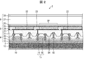
- FIG. 2 is a cross-sectional view showing a configuration example of the display area DA of the flexible organic EL display device 2.
- a resin layer 12 is formed on a translucent support substrate (for example, a mother glass substrate) that is peeled off and replaced with the lower surface film 10 (step S1).
- the barrier layer 3 is formed (step S2).
- the TFT layer 4 including the terminal TM and the wiring TW (see FIG. 1) is formed (step S3).
- the organic EL element layer 5 which is a light emitting element layer is formed as a display element (step S4).
- the sealing layer 6 is formed (step S5).
- a top film (not shown) is pasted on the sealing layer 6 (step S6).
- step S7 the resin layer 12 is irradiated with laser light through the support substrate to reduce the bonding force between the support substrate and the resin layer 12, and the support substrate is peeled from the resin layer 12 (step S7).
- This step is also referred to as a Laser Lift Off process (LLO process).
- LLO process Laser Lift Off process
- step S8 the lower surface film 10 is attached to the surface of the resin layer 12 from which the support substrate has been peeled off via an adhesive layer (not shown) (step S8).
- step S9 the laminate including the lower film 10, the resin layer 12, the barrier layer 3, the TFT layer 4, the organic EL element layer 5, the sealing layer 6 and the upper film is divided to obtain a plurality of pieces (step S9).
- an electronic circuit board for example, an IC chip
- ACF anisotropic conductive film
- step S10 edge folding (processing of bending 180 degrees with the folding slit CL shown in FIG. 1) is performed to obtain the flexible organic EL display device 2 (step S11).
- a disconnection inspection is performed, and if there is a disconnection, correction is performed (step S12).
- Examples of the material for the resin layer 12 include, but are not limited to, a polyimide resin, an epoxy resin, a polyamide resin, and the like.
- Examples of the material for the bottom film 10 include, but are not limited to, polyethylene terephthalate (PET).
- PET polyethylene terephthalate
- the barrier layer 3 is a layer that prevents moisture and impurities from reaching the TFT layer 4 and the organic EL element layer 5 when the flexible organic EL display device 2 is used.
- the barrier layer 3 is a silicon oxide film formed by CVD. , A silicon nitride film, a silicon oxynitride film, or a laminated film thereof.
- the TFT layer 4 is provided above the resin layer 12 and the barrier layer 3.
- the TFT layer 4 includes a semiconductor film 15, an inorganic insulating film 16 (gate insulating film) above the semiconductor film 15, a gate electrode GE above the inorganic insulating film 16, and an inorganic insulating film above the gate electrode GE.
- the TFT layer 4 includes, from the bottom film 10 (substrate) side, an inorganic insulating film 16 as a first inorganic layer, a gate electrode GE as a first metal layer, an inorganic insulating film 18 as a second inorganic layer, and / Or the inorganic insulating film 20, the source / drain wiring SH including the source / drain electrodes as the second metal layer and the terminal TM, and the planarizing film 21 as the first resin layer.
- a thin film transistor Tr (TFT) as an active element is configured to include the semiconductor film 15, the inorganic insulating film 16 (gate insulating film), the gate electrode GE, the inorganic insulating film 18, the inorganic insulating film 20, and the source / drain wiring SH.
- TFT thin film transistor Tr
- a common multiple layer inorganic film is formed at least in a partial region of the display area DA and the frame area NA, and the common multiple layer inorganic film includes: The barrier layer 3, the inorganic insulating film 16 (gate insulating film), the inorganic insulating film 18, and the inorganic insulating film 20 are included. That is, an inorganic laminate including the inorganic insulating film 16 as the first inorganic layer and the inorganic insulating film 18 and / or the inorganic insulating film 20 as the second inorganic layer in a part of the display area DA and the frame area NA. A film is formed.
- a frame area NA arranged outside the display area DA of the flexible organic EL display device 2 shown in FIG. 1 includes a terminal TM used for connection to an electronic circuit board such as an IC chip or FPC, a terminal TM and a display.
- a wiring TW that connects the signal lines in the area DA is formed.
- the terminal TM is provided at the end of the frame area NA.
- a signal input from the terminal TM is transmitted to a signal line (not shown) that is a wiring of the display area DA via the wiring TW.
- the semiconductor film 15 is made of, for example, low temperature polysilicon (LTPS) or an oxide semiconductor.
- LTPS low temperature polysilicon
- FIG. 2 the TFT having the semiconductor film 15 as a channel is shown as a top gate structure, but a bottom gate structure may be used (for example, when the TFT channel is an oxide semiconductor).
- the gate electrode GE, the capacitor electrode CE, the source / drain wiring SH, the wiring TW, and the terminal TM are, for example, aluminum (Al), tungsten (W), molybdenum (Mo), tantalum (Ta), chromium (Cr), titanium. It is composed of a single layer film or a laminated film of a metal containing at least one of (Ti) and copper (Cu).
- the inorganic insulating films 16, 18, and 20 can be formed of, for example, a silicon oxide (SiOx) film, a silicon nitride (SiNx) film, a silicon oxynitride film, or a laminated film thereof formed by a CVD method.
- the planarizing film (interlayer insulating film) 21 can be made of a photosensitive organic material that can be applied, such as polyimide resin or acrylic resin.
- the organic EL element layer 5 includes an anode 22 above the planarizing film 21, a bank 23 covering the edge of the anode 22, an EL (electroluminescence) layer 24 above the anode 22, and an upper layer than the EL layer 24. And each of the subpixels SP includes an island-shaped anode 22, an EL layer 24, and a cathode 25.
- the bank 23 (anode edge cover) 23 can be made of a photosensitive organic material that can be applied, such as polyimide resin or acrylic resin.
- the organic EL element layer 5 forms the display area DA and is provided in the upper layer of the TFT layer 4.
- the EL layer 24 is configured, for example, by laminating a hole injection layer, a hole transport layer, a light emitting layer, an electron transport layer, and an electron injection layer in order from the lower layer side.
- the light emitting layer is formed in an island shape for each subpixel by an evaporation method or an ink jet method, but the other layers may be a solid common layer.
- the structure which does not form one or more layers among a positive hole injection layer, a positive hole transport layer, an electron carrying layer, and an electron injection layer is also possible.
- the anode 22 is composed of, for example, a laminate of ITO (IndiumITOTin Oxide) and an alloy containing Ag, and has light reflectivity.
- the cathode 25 can be made of a light-transmitting conductive material such as ITO (Indium Tin Oxide) or IZO (Indium Zinc Oxide).
- the sealing layer 6 is translucent, and includes a first inorganic sealing film 26 that covers the cathode 25, an organic sealing film 27 that is formed above the first inorganic sealing film 26, and an organic sealing film 27. And a second inorganic sealing film 28 covering the surface.
- the sealing layer 6 covering the organic EL element layer 5 prevents penetration of foreign matters such as water and oxygen into the organic EL element layer 5.
- Each of the first inorganic sealing film 26 and the second inorganic sealing film 28 may be composed of, for example, a silicon oxide film, a silicon nitride film, a silicon oxynitride film, or a laminated film formed by CVD. it can.
- the organic sealing film 27 is a light-transmitting organic film that is thicker than the first inorganic sealing film 26 and the second inorganic sealing film 28, and is composed of a photosensitive organic material that can be applied such as polyimide resin or acrylic resin. can do.
- the present invention is not limited thereto.
- a flexible substrate having high heat resistance that can withstand the temperatures in the steps S1 to S5 described above is used as the substrate, it is not necessary to replace the substrate, and thus the above-described steps S7 and S8. Can be omitted.
- FIG. 3A is a cross-sectional view illustrating a portion A of the flexible organic EL display device 2 illustrated in FIG. 1, and FIG. 3B is a plan view of the vicinity of the terminal TM of the flexible organic EL display device 2.
- 3C is a cross-sectional view taken along the line AA ′ of the flexible organic EL display device 2 of the first embodiment illustrated in FIG. 3B
- FIG. 3D is a cross-sectional view of FIG.
- FIG. 2B is a cross-sectional view taken along line BB ′ of the flexible organic EL display device 2 according to the first embodiment illustrated in FIG.
- the flexible organic EL display device 2 includes a display layer DA including a TFT layer 4 including a thin film transistor Tr (TFT) and an organic EL element layer 5 on the resin layer 12 and the barrier layer 3 provided on the lower film 10 (see FIG. 2), and a frame area NA provided around the display area DA shown in FIG. 3A.
- TFT thin film transistor Tr
- FIG. 3A shows a partial area of the frame area NA provided around the display area DA.
- the partial area of the frame area NA includes a plurality of terminals TM, bending slits CL, and the like. Is formed.
- a barrier layer 3 an inorganic insulating film 16, an inorganic insulating film 18, An inorganic insulating film 20 is formed.
- Each of the plurality of terminals TM is a part of each of the plurality of wirings TW that inputs signals from the outside to a part of the plurality of thin film transistors Tr (TFT) illustrated in FIG.
- Each of the plurality of terminals TM is a part of each of the plurality of wirings TW and may be formed slightly thicker than the other parts.
- each of the plurality of terminals TM is a part of each of the plurality of wirings TW exposed through the opening 8a of the second resin layer 8. As illustrated in FIG.
- each of the plurality of wirings TW includes a fourth conductive member G1a and a lead wiring G2a formed of the same material as the gate electrode GE that is the first metal layer, and a source that is the second metal layer.
- a first conductive member SH1a and a third conductive member SH2a formed of the same material as the source / drain wiring SH including the drain electrode are included.
- Each of the plurality of terminals TM includes the third conductive member SH2a that is the second metal layer exposed through the opening 8a of the second resin layer 8.
- the routing wiring G2a and the third conductive member SH2a which is the second metal layer are electrically connected by a third contact hole CH3 formed in the inorganic insulating film 18 and the inorganic insulating film 20 as a second inorganic layer. Yes.
- the folding slit CL is a first direction (vertical direction in the drawing) that is the extending direction of each of the plurality of wirings TW in a partial region of the frame region NA.
- first direction vertical direction in the drawing
- present invention is not limited to this.
- present invention is not limited to this.
- the bending slit CL is an inorganic laminate of the barrier layer 3, the inorganic insulating film 16, the inorganic insulating film 18, and the inorganic insulating film 20.
- the film is formed by removing all the film, but the present invention is not limited to this, and at least a part of the inorganic laminated film of the barrier layer 3, the inorganic insulating film 16, the inorganic insulating film 18, and the inorganic insulating film 20 is formed. It may be formed by removing.
- the step of forming the bending slit CL is after the step of forming the inorganic laminated film of the barrier layer 3, the inorganic insulating film 16, the inorganic insulating film 18, and the inorganic insulating film 20, and the third resin layer. Is performed before the step of forming the convex portion 7b, and at least part of the inorganic laminated film of the barrier layer 3, the inorganic insulating film 16, the inorganic insulating film 18, and the inorganic insulating film 20 is dry-etched, for example. It is the process of removing by the method etc. and forming the bending slit CL.
- the folding slit CL is filled with the third resin layer 7a that is the same layer as the convex portion 7b, and each of the third resin layer 7a and the plurality of terminals TM is formed as a layer filling the bending slit.
- the convex portion 7b is made of the same material. For example, after applying a photosensitive organic material such as polyimide resin or acrylic resin, exposure and development are performed, and the predetermined shape is simultaneously formed in one process.
- a photosensitive organic material such as polyimide resin or acrylic resin
- exposure and development are performed, and the predetermined shape is simultaneously formed in one process.
- the present invention is not limited to this, and different materials may be used and formed at different timings in different processes.
- the height of each of the third resin layer 7a and the convex portion 7b is set.
- the present invention is not limited to this, and the height of each of the third resin layer 7a and the convex portion 7b can be set in one process using the same material by using a halftone mask. Different processes using different materials can be formed differently by different exposure doses.
- the fourth conductive member G1a and the first conductive member SH1a formed on the display area DA side (left side in the drawing) from the bending slit CL are formed on the inorganic insulating film 18 and the inorganic insulating film 20.
- the lead wiring G2a electrically connected through the first contact hole CH1 and formed on the terminal TM side (right side in the drawing) from the bending slit CL, and the first conductive member SH1a include the inorganic insulating film 18 and They are electrically connected via a second contact hole CH2 formed in the inorganic insulating film 20.
- the second resin layer 8 for example, a photosensitive organic material that can be applied such as polyimide resin or acrylic resin can be used.
- planarizing film 21 and the second resin layer 8 as the first resin layer are formed of the same material, they can be formed by the same process.
- the present invention is not limited to this. Absent.
- the third resin layer 7a as a layer filling the bending slit and the convex portion 7b are formed only in the frame area NA will be described as an example, but the third resin layer 7a is described. And the layer which forms the convex part 7b may be formed in the display area DA.
- the third resin layer is formed between the source / drain wiring SH including the source / drain electrodes as the second metal layer in the TFT layer 4 and the planarizing film 21 as the first resin layer. Is done.
- the present invention as illustrated in FIG. 3A, the case where the second resin layer 8 is divided will be described as an example. However, the present invention is not limited thereto, and the second resin is not limited thereto.
- the layers 8 may be connected as one layer.
- the side surfaces of the third resin layer 7a and the convex portion 7b are shown at substantially right angles, but in practice, the first conductive member SH1a, the third conductive member SH2a, Therefore, the side surfaces of the third resin layer 7a and the convex portion 7b are formed to have a taper angle of less than 90 degrees.
- the convex portion 7b is the extending direction of each of the plurality of wirings TW. Formed as one island-like layer whose width in the second direction (left and right direction in FIG. 3 (b)) perpendicular to the first direction is wider than the width in the first direction (up / down direction in FIG. 3 (b)) doing.
- the third conductive member SH2a / SH2b / SH2c which is the second metal layer includes a portion exposed by the opening 8a of the second resin layer 8.
- Narrow width including a wide area SH2a-2, SH2b-2, SH2c-2, and a portion extending from the wide area to the display area DA and electrically connected to the routing wirings G2a, G2b, G2c,. It has areas SH2a-1, SH2b-1, SH2c-1,.
- R1 is equal to the adjacent wide regions SH2a-2, SH2b-2, SH2c-2 of the third conductive members SH2a, SH2b, SH2c,. Is larger than the interval R2.
- the plurality of terminals TM and the protrusions 7b are connected to the routing wirings G2a, G2b, It arrange
- the ends of the convex portions 7b are arranged between the adjacent wide regions SH2a-2, SH2b-2, SH2c-2,... (Interval R2) of the third conductive members SH2a, SH2b, SH2c,.
- Interval R2 the third conductive members SH2a, SH2b, SH2c, since the interval is narrow, a residue is likely to occur in the convex portion 7b, and leakage is likely to occur between the third conductive members SH2a, SH2b, SH2c,.
- the fourth conductive member G1a and the routing wiring G2a are made of the same material as the metal material forming the gate electrode GE in the thin film transistor Tr shown in FIG. 2, and the first conductive member SH1a and the third conductive member G1a are formed.
- the conductive member SH2a is formed of the same material as the metal material forming the source / drain wiring SH in the thin film transistor Tr illustrated in FIG. 2, and each of the plurality of wirings TW is illustrated in FIG.
- the capacitance element shown in FIG. 2 is not included in each of the plurality of wirings TW.
- Capacitor wiring CE may be a metal material and same material is used to form a contained.
- the plurality of terminals TM are formed of the same material as the metal material forming the source / drain wiring SH in the thin film transistor Tr illustrated in FIG.
- the flexible organic EL display device 2 provided with the bending slit CL has been described as an example. However, it is necessary to provide the bending slit CL or the flexible display device (flexible display device).
- the non-flexible display device non-flexible display device
- the plurality of terminals TM are formed of the same material as the metal material forming the source / drain wiring SH in the thin film transistor Tr shown in FIG.
- the convex portion 7b formed of the third resin layer which is a layer below the second resin layer 8, and the third conductive members SH2a, SH2b, If SH2c...
- the terminal TM since the plurality of terminals TM are formed on the convex portion 7b and can be increased in height, the electronic circuit board can be easily mounted on the terminals TM.
- Embodiment 2 of the present invention will be described based on FIG.
- the convex portions 7 e 1, 7 e 2, 7 e 3... are formed in a plurality of island shapes for a plurality of terminals. Is as described in the first embodiment.
- members having the same functions as those shown in the drawings of Embodiment 1 are given the same reference numerals, and descriptions thereof are omitted.
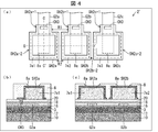
- FIG. 4A is a plan view of the vicinity of a terminal of the flexible organic EL display device 2 ′
- FIG. 4B is a flexible organic EL display device according to the second embodiment illustrated in FIG.
- FIG. 4C is a cross-sectional view taken along the line DD ′ of the flexible organic EL display device 2 ′ according to the second embodiment illustrated in FIG. 4A.
- FIG. 4A is a plan view of the vicinity of a terminal of the flexible organic EL display device 2 ′
- FIG. 4B is a flexible organic EL display device according to the second embodiment illustrated in FIG.
- FIG. 4C is a cross-sectional view taken along the line DD ′ of the flexible organic EL display device 2 ′ according to the second embodiment illustrated in FIG. 4A.
- FIG. 4A is a plan view of the vicinity of a terminal of the flexible organic EL display device 2 ′
- FIG. 4B is a flexible organic EL display device according to the second embodiment illustrated in FIG.
- FIG. 4C is
- the flexible organic EL display device 2 ′ includes a plurality of convex portions 7e1, 7e2, 7e3,. Each terminal is formed into a plurality of islands. Further, the surfaces of the plurality of island-shaped convex portions 7e1, 7e2, 7e3,... Are covered with the third conductive members SH2a, SH2b, SH2c,. It has been broken.
- the wiring lines G2a, G2b, G2c,... are linearly arranged in a direction perpendicular to the extending direction. Accordingly, it is possible to suppress the generation of residues on the convex portions 7e1, 7e2, 7e3, ... during the patterning of the second metal layer.
- the present invention is not limited to this.
- the flexible organic EL display device 2 ′′ of the present embodiment includes a first terminal group and a second terminal group, and the first terminal group shares the first convex portion 7b ′ and the second terminal group.
- the terminal group is different from the first and second embodiments in that the second convex portion 7b is shared, and the other is as described in the first and second embodiments.
- members having the same functions as those shown in the drawings of Embodiments 1 and 2 are given the same reference numerals, and descriptions thereof are omitted.
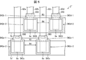
- FIG. 5 is a plan view of the vicinity of the terminals of the flexible organic EL display device 2 ′′.
- the first terminal group which is the lower terminal group in the figure, is a plurality of routing wirings G2a, G2b, G2c, G2d,..., Among the routing wirings G2a, G2c,.
- a terminal group in which a plurality of terminals electrically connected to are arranged in a direction (horizontal direction in the figure) perpendicular to the extending direction (vertical direction in the figure) of the routing wirings G2a, G2b, G2c, G2d. is there.
- the second terminal group which is the upper terminal group in the figure, is electrically connected to a plurality of routing wires G2a, G2b, G2c, G2d... And routing wires G2b, G2d.
- routing wires G2a, G2b, G2c, G2d are a group of terminals arranged in a direction (horizontal direction in the figure) perpendicular to the extending direction (vertical direction in the figure) of the routing wirings G2a, G2b, G2c, G2d.
- the first protrusion 7b 'and the second protrusion 7b extend in a direction (horizontal direction in the figure) perpendicular to the extension direction (vertical direction in the figure) of the routing wirings G2a, G2b, G2c, G2d,. Is formed.
- the first terminal group which is the lower terminal group in the figure, shares the first convex part 7b '
- the second terminal group which is the upper terminal group in the figure, shares the second convex part 7b.
- a plurality of terminals are arranged alternately in the extending direction (vertical direction in the figure) of the routing wirings G2a, G2b, G2c, G2d,.
- Forming the second terminal group so that the first terminal group can share the first convex part 7b ', and the second terminal group can share the second convex part 7b.
- a first protrusion 7b ′ and a second protrusion 7b are formed.
- the first terminal group and the convex portion 7b ′ are routed in consideration of the fact that a residue is likely to remain during the patterning of the second metal layer.
- the wires G2a, G2b, G2c,... are linearly arranged in the direction perpendicular to the extending direction of the wires G2a, G2b, G2c,. They are arranged in a straight line in a direction perpendicular to the stretching direction.
- the interval R3 of 1 ⁇ SH2d-1... Is larger than the interval R1 described in the first embodiment.
- the distance R4 between the adjacent wide regions SH2a-2, SH2c-2,... And the interval R4 between the adjacent wide regions SH2b-2, SH2d-2,... Of the third conductive members SH2a, SH2b, SH2c. Is larger than the interval R2 described in the first embodiment.
- one end of the convex portion 7b ′ is disposed between the adjacent wide regions SH2a-2, SH2c-2,... (Interval R4) of the third conductive members SH2a, SH2c,.
- the one end of the convex portion 7b is disposed between the adjacent narrow regions SH2b-1, SH2d-1,... (Interval R3) of the third conductive members SH2b, SH2d,.
- the flexible organic EL display device 2 ′ ′′ of the present embodiment includes a first terminal group and a second terminal group, and the protrusions 7e1 ′, 7e1, 7e2 ′, 7e2,.
- the third embodiment is different from the third embodiment in that a plurality of islands are formed for each terminal group and each terminal of the second terminal group, and the others are as described in the third embodiment.
- members having the same functions as those shown in the drawings of the third embodiment are given the same reference numerals, and descriptions thereof are omitted.
- FIG. 6 is a plan view of the vicinity of the terminals of the flexible organic EL display device 2 ′′ ′′.
- the first terminal group which is the lower terminal group in the figure, is a plurality of routing wirings G2a, G2b, G2c, G2d,..., Among the routing wirings G2a, G2c,.
- a terminal group in which a plurality of terminals electrically connected to are arranged in a direction (horizontal direction in the figure) perpendicular to the extending direction (vertical direction in the figure) of the routing wirings G2a, G2b, G2c, G2d. is there.
- the second terminal group which is the upper terminal group in the figure, is electrically connected to a plurality of routing wires G2a, G2b, G2c, G2d... And routing wires G2b, G2d.
- routing wires G2a, G2b, G2c, G2d are a group of terminals arranged in a direction (horizontal direction in the figure) perpendicular to the extending direction (vertical direction in the figure) of the routing wirings G2a, G2b, G2c, G2d.
- the convex portions 7e1 ′, 7e1, 7e2 ′, 7e2,... are formed in a plurality of islands for each of the terminals of the first terminal group and the second terminal group, and lead wirings G2a, G2b, G2c, G2d.
- the width of each of the third conductive members SH2a, SH2b, SH2c In the direction perpendicular to the stretching direction (vertical direction in the figure) (horizontal direction in the figure), the width of each of the third conductive members SH2a, SH2b, SH2c,. It is smaller than the width of each of the convex portions 7e1 ′, 7e1, 7e2 ′, 7e2,.
- the first terminal group and the protrusions 7e1 ′ and 7e2 ′ are taken into consideration that residues are likely to remain during the patterning of the second metal layer.
- the wiring lines G2a, G2b, G2c,... are linearly arranged in a direction perpendicular to the extending direction.
- the third conductive members SH2a, SH2b, and SH2c are arranged in the direction perpendicular to the extending direction of the lead wirings G2a, G2b, G2c,.
- the distance R6 between the adjacent wide areas SH2a-2, SH2c-2,... And the distance R6 between the adjacent wide areas SH2b-2, SH2d-2,... are adjacent to the convex portions 7e1, 7e2,. Is larger than the interval R5 and the interval R5 between the adjacent convex portions 7e1 ′, 7e2 ′,.
- the interval between SH2b-1, SH2d-1,... Is larger than the interval R1 described in the first embodiment.
- the spacing R6 between the adjacent wide regions SH2a-2, SH2c-2,... And the spacing R6 between the adjacent wide regions SH2b-2, SH2d-2,... Of the third conductive members SH2a, SH2b, SH2c. Is larger than the interval R2 described in the first embodiment.
- Embodiment 5 of the present invention will be described with reference to FIG.
- an inorganic laminate of a barrier layer 3, an inorganic insulating film 16, an inorganic insulating film 18, and an inorganic insulating film 20 is provided between the bending slit CL and the plurality of terminals TM.
- the first slit SL1 from which at least a part of the film is removed is provided, and the others are as described in the first to fourth embodiments.
- members having the same functions as those shown in the drawings of Embodiments 1 to 4 are given the same reference numerals, and descriptions thereof are omitted.
- FIG. 7A is a cross-sectional view showing a part of the frame area NA of the flexible organic EL display device 2a
- FIG. 7B shows the vicinity of the first slit SL1 of the flexible organic EL display device 2a. It is a top view.
- the flexible organic EL display device 2a is provided in a partial region of the frame region NA, like the bending slit CL in the first embodiment described above. And a first slit SL1 that is one opening formed from one end to the other end in the second direction orthogonal to the first direction that is the extending direction of each of the plurality of wirings TW. Yes.
- the first slit SL1 is formed by removing the inorganic insulating film 18 and the inorganic insulating film 20 in a portion where the routing wirings G2a, G2b, G2c, G2d, and G2e are formed.
- the barrier layer 3, the inorganic insulating film 16, the inorganic insulating film 18, and the inorganic insulating film 20 are removed to form one opening.
- the one opening exposes part of the routing wirings G2a, G2b, G2c, G2d, and G2e formed of the same material as the metal material that forms the gate electrode GE in the thin film transistor Tr shown in FIG.
- each of the routing wirings G2a, G2b, G2c, G2d, and G2e intersects the first slit SL1 and is formed in a lower layer than the first slit SL1.
- the first slit SL1 is filled with the second resin layer 8.
- the present invention is not limited to this, and a plurality of slits may be provided as in the seventh embodiment described later. It may be an opening.
- the flexible organic EL display device 2a since the flexible organic EL display device 2a includes the first slit SL1, when the electronic circuit board is mounted on the terminal TM, cracks are generated in the inorganic insulating film 18 and the inorganic insulating film 20 which are base films of the terminal TM. Even so, the first slit SL1 can prevent the crack from spreading toward the display area DA.
- the step of forming the first slit SL1 and the step of forming the bending slit CL may be one (same) step.
- the first slit SL1 and the bending slit CL may be It can be formed by one dry etching process.
- the flexible organic EL display device 2a provided with the folding slit CL has been described as an example. However, it is necessary to provide the folding slit CL or the flexible display device (flexible display device). Alternatively, a non-flexible display device (non-flexible display device) may be used.
- Embodiment 6 of the present invention will be described with reference to FIG.
- a part of the routing wirings G2a, G2b, G2c, G2d, and G2e exposed from the first slit SL1 provided between the bending slit CL and the plurality of terminals TM. Is covered with each of a plurality of second conductive members SH3a, SH3b, SH3c, SH3d, and SH3e that are formed in the same shape as the metal material that forms the source / drain wiring SH in the thin film transistor Tr shown in FIG.
- the other points are as described in the fifth embodiment.
- members having the same functions as those shown in the drawings of Embodiment 5 are given the same reference numerals, and descriptions thereof are omitted.
- FIG. 8A is a cross-sectional view showing a part of the frame area NA of the flexible organic EL display device 2b
- FIG. 8B shows the vicinity of the first slit SL1 of the flexible organic EL display device 2b. It is a top view.
- each of the plurality of routing wirings G2a, G2b, G2c, G2d, and G2e overlapping the first slit SL1 is covered with each of the second conductive members SH3a, SH3b, SH3c, SH3d, and SH3e.
- the first conductive members SH1a, SH1b, and SH1c formed of the same material as the metal material that forms the source / drain wirings SH in the thin film transistor Tr illustrated in FIG.
- the third conductive member SH2a / SH2b / SH2c / SH2d / SH2e, and the plurality of second conductive members SH3a / SH3b / SH3c / SH3d / SH3e into a predetermined shape
- the first A part of the routing wiring G2a, G2b, G2c, G2d, and G2e exposed from the slit SL1 can be protected by a plurality of second conductive members SH3a, SH3b, SH3c, SH3d, and SH3e.
- the same metal material that forms the source / drain wiring SH in the thin film transistor Tr shown in FIG. 7A the same metal material that forms the source / drain wiring SH in the thin film transistor Tr shown in FIG.
- the first conductive member SH1a / SH1b / SH1c / SH1d / SH1e formed of the material and the third conductive member SH2a / SH2b / SH2c / SH2d / SH2e are patterned into a predetermined shape, the first slit SL1 is formed.
- a portion of the routing wiring G2a, G2b, G2c, G2d, and G2e exposed from the first slit SL1 is not protected by the plurality of second conductive members SH3a, SH3b, SH3c, SH3d, and SH3e. A part of the routing wiring G2a, G2b, G2c, G2d, G2e is damaged. There.
- the present invention is not limited to this, and a plurality of slits may be provided as in the seventh embodiment described later. It may be an opening.
- Embodiment 7 of the present invention will be described with reference to FIG.
- the first slits SL2a, SL2b, SL2c, SL2d, and SL2e provided between the bending slit CL and the plurality of terminals TM are a plurality of openings.
- the other points are as described in Embodiments 5 and 6.
- members having the same functions as those shown in the drawings of Embodiments 5 and 6 are given the same reference numerals, and descriptions thereof are omitted.
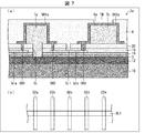
- FIG. 9A is a cross-sectional view showing a part of the frame area NA of the flexible organic EL display device 2c
- FIG. 9B shows the first slits SL2a and SL2b of the flexible organic EL display device 2c. It is a plan view in the vicinity of SL2c, SL2d, and SL2e.
- the first slits SL2a, SL2b, SL2c, SL2d, and SL2e are a plurality of openings, and therefore the first slits SL2a, SL2b, Each of SL2c, SL2d, and SL2e exposes a part of the routing wiring G2a, G2b, G2c, G2d, and G2e.
- each of the first slits SL2a, SL2b, SL2c, SL2d, SL2e,..., Which is a plurality of openings, has a first slit group SL2a, as shown in FIG. SL2c, SL2e,... And second slit groups SL2b, SL2d,.
- Part of the plurality of island-shaped first slits is a slit group arranged in a direction perpendicular to the extending direction of the routing wirings G2a, G2b, G2c, G2d, G2e,.
- the second slit groups SL2b, SL2d,... Intersect the routing lines G2b, G2d,... That are not adjacent to each other among the plurality of routing lines G2a, G2b, G2c, G2d, G2e,.
- a portion of the slits other than the part of the first slit is a slit group arranged in a direction perpendicular to the extending direction of the routing wiring.
- each of the first slits SL2a, SL2b, SL2c, SL2d, and SL2e which is a plurality of openings, overlaps with each of the routing wirings G2a, G2b, G2c, G2d, and G2e,
- Each of the slits SL2a, SL2b, SL2c, SL2d, and SL2e exposes a part of each of the routing wirings G2a, G2b, G2c, G2d, and G2e.
- the first slit SL1 that is one opening in the fifth and sixth embodiments described above, it is formed of the same material as the metal material for forming the source / drain wiring SH in the thin film transistor Tr shown in FIG. As a result, it is easy to leave a residue between the plurality of wirings TW.
- each of the first slits SL2a, SL2b, SL2c, SL2d, and SL2e which is a plurality of openings, overlaps with each of the routing wirings G2a, G2b, G2c, G2d, and G2e. Even if a residue remains at each end of each of the slits SL2a, SL2b, SL2c, SL2d, and SL2e, this residue does not affect the adjacent wiring TW, so that leakage occurs between each of the plurality of wirings TW. Can be suppressed.
- Part of the routing wirings G2a, G2b, G2c, G2d, G2e,... Exposed from the substrate is formed in an island shape with the same material as the metal material forming the source / drain wiring SH in the thin film transistor Tr shown in FIG.
- the first conductive members SH1a, SH1b, and SH1c formed of the same material as the metal material that forms the source / drain wirings SH in the thin film transistor Tr illustrated in FIG.
- the frame area NA is provided outside the partial area of the frame area NA where the plurality of terminals TM are formed, and the second slit SL8 is provided.
- the first slit SL7 filled with the third resin layer 7c, which is the same material as the convex portion 7b, with the same material as the metal material for forming the source / drain wiring SH in the thin film transistor Tr shown in FIG.
- the third conductive members SH5a, SH5b, SH5c, SH5d, SH5e,... are different from the first to seventh embodiments, and the others are as described in the first to seventh embodiments.
- members having the same functions as those shown in the drawings of Embodiments 1 to 7 are given the same reference numerals, and descriptions thereof are omitted.
- FIG. 10A is a cross-sectional view showing a part of the frame area NA of the flexible organic EL display device 2d
- FIG. 10B is a plan view in the vicinity of the terminal TM of the flexible organic EL display device 2d. is there.
- the flexible organic EL display device 2d is a frame area NA, which is a partial area of the frame area NA in which a plurality of terminals TM are formed.
- a second slit SL8 is provided, and the second slit SL8 is filled with a third resin layer 7d made of the same material as that of the convex portion 7b.
- the inner side of the partial area of the frame area NA where the plurality of terminals TM are formed is an area in contact with the display area DA.
- the flexible organic EL display device 2d is formed by removing the barrier layer 3, the inorganic insulating film 16, the inorganic insulating film 18, and the inorganic insulating film 20 between the bending slit CL and the plurality of terminals TM.
- the barrier layer 3, the inorganic insulating film 16, and the outside of a part of the frame area NA in which the plurality of terminals TM are formed are provided in the frame area NA.
- a second slit SL8 formed by removing the inorganic insulating film 18 and the inorganic insulating film 20 is also provided.
- the first slit SL7 can suppress the crack from spreading to the display area DA, and the second slit SL8 can suppress the crack from spreading to the outside of the second slit SL8.
- the first slit SL7 is filled with a third resin layer 7c made of the same material as the convex portion 7b, and the source / drain wiring SH in the thin film transistor Tr shown in FIG. 2 is formed on the third resin layer 7c.
- Third conductive members SH5a, SH5b, SH5c, SH5d, SH5e,... Formed of the same material as the metal material to be formed are formed.
- the part formed on the convex part 7b is the terminal TM.
- each of the routing wirings G2a, G2b, G2c, G2d, G2e,... Is electrically connected to each of the third conductive members SH5a, SH5b, SH5c, SH5d, SH5e,. It is connected.
- the first slit SL7 does not expose each of the routing wirings G2a, G2b, G2c, G2d, G2e..., And the first slit SL7 is made of the same material as the convex portion 7b. Since the third conductive member SH5a, SH5b, SH5c, SH5d, SH5e is formed on the third resin layer 7c and filled with a certain third resin layer 7c, the end of the first slit SL7 is shown in FIG. The residue of the layer formed of the same material as the metal material for forming the source / drain wiring SH in the thin film transistor Tr shown in FIG.
- the third resin layer 7a that is a layer that fills the bending slit CL
- the third resin layer 7b that forms the plurality of terminals TM
- FIG. 10 is a plan view of the vicinity of a terminal of a flexible organic EL display device 2e which is a modification of the flexible organic EL display device 2d.
- the convex portions 7e1, 7e2, 7e3,. ⁇ Is a plurality of island-like layers, and the convex portions 7e1, 7e2, 7e3, ... are formed for each of a plurality of terminals.
- the third slit SL9 is filled with a third resin layer 7f, which is the same material as the layer forming the convex portions 7e1, 7e2, 7e3.
- the third slit SL9 can prevent the crack from spreading in the left-right direction in the drawing, that is, in the direction of the adjacent wiring TW.
- the present invention is not limited to this, and the first slit SL7 as in the above-described seventh embodiment.
- a plurality of openings may be formed as one slit.
- a substrate a display element constituting a display region provided on the substrate via a TFT layer, a frame region provided around the display region, and provided at an end of the frame region.
- a display device including a terminal for inputting a signal,
- the TFT layer includes, from the substrate side, a first inorganic layer, a first metal layer, a second inorganic layer, a second metal layer, and a first resin layer,
- a lead wiring that transmits a signal from the terminal to the signal line of the display region is formed, and the lead wiring is formed of the first metal layer
- the terminal is composed of the second metal layer exposed through the opening of the second resin layer, In the opening of the second resin layer, the convex portion formed by the third resin layer, which is a lower layer than the second resin layer, and the second metal layer overlap,
- the display device wherein the routing wiring and the second metal layer are electrically connected by a contact hole formed in the second inorganic layer.
- the second metal layer includes a wide region including a portion exposed by the opening of the second resin layer, and a narrow width including a portion extending from the wide region to the display region side and electrically connected to the routing wiring. And having an area In a direction perpendicular to the extending direction of the routing wiring, an interval between the narrow regions adjacent to the second metal layer is larger than an interval between the adjacent wide regions of the second metal layer,
- a plurality of the lead wiring, the second metal layer, and the contact hole are formed, Each of the plurality of routing wires and each of the plurality of second metal layers are electrically connected by each of the plurality of contact holes,
- the plurality of terminals including the terminal are each composed of the plurality of second metal layers exposed by the opening of the second resin layer, and are formed in a direction perpendicular to the extending direction of the routing wiring,
- the convex portion is formed by extending in a direction perpendicular to the extending direction of the routing wiring,
- the display device according to aspect 1 or 2, wherein the plurality of terminals share the convex portion.
- a plurality of the lead wiring, the second metal layer, and the contact hole are formed, Each of the plurality of routing wires and each of the plurality of second metal layers are electrically connected by each of the plurality of contact holes,
- the plurality of terminals including the terminal are each composed of the plurality of second metal layers exposed by the opening of the second resin layer, and are formed of a first terminal group and a second terminal group, The first terminal group is arranged in a direction perpendicular to the extending direction of the routing wiring, wherein the plurality of terminals are electrically connected to the routing wiring not adjacent to each other in the plurality of routing wirings.
- the second terminal group is electrically connected to routing wires that are not adjacent to each other in the plurality of routing wires, except for the portions of the plurality of terminals that are perpendicular to the extending direction of the routing wires.
- a group of terminals arranged, The convex portion is formed by a first convex portion and a second convex portion formed by extending in a direction perpendicular to the extending direction of the routing wiring, The first terminal group shares the first convex portion, The display device according to claim 1, wherein the second terminal group shares the second convex portion.
- a plurality of the lead wiring, the second metal layer, and the contact hole are formed, Each of the plurality of routing wires and each of the plurality of second metal layers are electrically connected by each of the plurality of contact holes,
- the plurality of terminals including the terminal are each composed of the plurality of second metal layers exposed by the opening of the second resin layer, and are formed in a direction perpendicular to the extending direction of the routing wiring,
- the plurality of terminals are formed of a first terminal group and a second terminal group,
- the first terminal group is arranged in a direction perpendicular to the extending direction of the routing wiring, wherein the plurality of terminals are electrically connected to the routing wiring not adjacent to each other in the plurality of routing wirings.
- Terminal group, The second terminal group is electrically connected to routing wires that are not adjacent to each other in the plurality of routing wires, except for the portions of the plurality of terminals that are perpendicular to the extending direction of the routing wires.
- a group of terminals arranged, The convex portion is formed in a plurality of island shapes for each terminal of the first terminal group and the second terminal group, 6.
- the display device according to aspect 5, wherein the interval between the adjacent second metal layers is larger than the interval between the adjacent convex portions in a direction perpendicular to the extending direction of the routing wiring.
- the substrate is a flexible substrate, In the frame region, an inorganic laminated film including the first inorganic layer and the second inorganic layer is formed, A bending slit from which at least a part of the inorganic laminated film is removed is formed from one end of the flexible substrate in the direction perpendicular to the extending direction of the routing wiring to the other end.
- the bending slit is filled with the same material as the third resin layer, Between the bending slit and the terminal, a first slit from which at least a part of the inorganic laminated film is removed is formed, The routing wiring is electrically connected to a first conductive member formed of the same material as the second metal layer, The first conductive member intersects with the bending slit filled with the same material as the third resin layer, The display device according to any one of aspects 1 to 8, wherein the routing wiring intersects with the first slit and is formed in a lower layer than the first slit.
- the aspect 9 is characterized in that the first slit is formed from one end to the other end of the flexible substrate in a direction perpendicular to the extending direction of the routing wiring. Display device.
- a plurality of the lead wiring, the second metal layer, and the contact hole are formed, Each of the plurality of routing wires and each of the plurality of second metal layers are electrically connected by each of the plurality of contact holes,
- the first slit is formed in a plurality of islands for each of the plurality of routing wires, Each of the plurality of routing wires intersects each of the plurality of island-shaped first slits,
- the plurality of island-shaped first slits are formed by a first slit group and a second slit group, In the plurality of routing lines, the first slit group intersects with routing lines that are not adjacent to each other, and a part of the plurality of island-shaped first slits is arranged in a direction perpendicular to the extending direction of the routing lines.
- the second slit group intersects with routing wires that are not adjacent to each other among the plurality of routing wires, except for the portions of the plurality of island-shaped first slits that are perpendicular to the extending direction of the routing wires.
- the substrate is a flexible substrate, In the frame region, an inorganic laminated film including the first inorganic layer and the second inorganic layer is formed, A bending slit from which at least a part of the inorganic laminated film is removed is formed from one end of the flexible substrate in the direction perpendicular to the extending direction of the routing wiring to the other end.
- a first slit from which at least a part of the inorganic laminated film is removed is formed,
- the bending slit and the first slit are filled with the same material as the third resin layer,
- the routing wiring is electrically connected to a first conductive member formed of the same material as the second metal layer,
- the first conductive member intersects with the bending slit filled with the same material as the third resin layer,
- the display device according to any one of aspects 1 to 8, wherein the second metal layer intersects with the first slit filled with the same material as the third resin layer.
- a terminal for inputting a signal, and a manufacturing method of a display device comprising: Including a step of forming a first inorganic layer, a step of forming a first metal layer, a step of forming a second inorganic layer, a step of forming a second metal layer, and a step of forming a first resin layer.
- the first inorganic layer is formed on the substrate, In the step of forming the first metal layer, a lead-out wiring that transmits a signal from the terminal to a signal line of the display area is provided in the frame area between the display area and the terminal. Formed on the inorganic layer, In the step of forming the second inorganic layer, after forming the second inorganic layer so as to cover the routing wiring, a contact hole is formed in a portion overlapping the routing wiring in the second inorganic layer.
- a convex portion is formed on the second inorganic layer
- the second metal layer is formed so as to overlap with the convex portion and to be electrically connected to the routing wiring through the contact hole
- an opening is formed at a position where the convex portion and the second metal layer overlap each other.
- the present invention can be used for a display device and a method for manufacturing the display device.
- 3rd conductive member (2nd metal layer) SH2a ... third conductive member (second metal layer) G1a ... fourth conductive member SH2a-1 ... narrow region of third conductive member (narrow region of second metal layer) SH2a-2... Wide area of the third conductive member (wide area of the second metal layer) SH5a-1 ... Narrow region of third conductive member (narrow region of second metal layer) SH5a-2...
Landscapes
- Physics & Mathematics (AREA)
- Engineering & Computer Science (AREA)
- General Physics & Mathematics (AREA)
- Nonlinear Science (AREA)
- Theoretical Computer Science (AREA)
- Microelectronics & Electronic Packaging (AREA)
- Mathematical Physics (AREA)
- Chemical & Material Sciences (AREA)
- Crystallography & Structural Chemistry (AREA)
- Optics & Photonics (AREA)
- Manufacturing & Machinery (AREA)
- Electroluminescent Light Sources (AREA)
Abstract
フレキシブル有機EL表示装置(2)の端子(TM)は、第2樹脂層(8)の開口(8a)によって露出した第2の金属層である第3導電部材(SH2a)から成り、第2樹脂層(8)の開口(8a)において、第2樹脂層(8)より下層である第3樹脂層で形成された凸部(7b)と第2の金属層である第3導電部材(SH2a)とが重畳する。
Description
本発明は、表示装置及び表示装置の製造方法に関する。
特許文献1には、外部から信号を供給するための端子(パッド)を備えた表示装置について開示されている。
特許文献1に開示されている従来の表示装置においては、膜厚の厚い保護膜上に端子(パッド)を形成するため、上記表示装置に備えられたトランジスタ素子(TFT素子)を覆う層である上記保護膜より上層である画素電極を形成する層(陽極または陰極を形成する層ともいう)を用いて、端子(パッド)を形成している。
しかしながら、上記画素電極を形成する層(陽極または陰極を形成する層)の場合、ITO(Indium Tin Oxide)やIZO(Indium Zinc Oxide)等の導電材を含むのが一般的であるため、上記表示装置に備えられたトランジスタ素子(TFT素子)におけるソース電極及びドレイン電極を形成する金属層などと比較すると、その強度が弱く、上記画素電極を形成する層(陽極または陰極を形成する層)を用いて形成された端子(パッド)の場合、端子に電子回路基板を実装する時に、容易に破損してしまうという問題がある。
本発明は、上記の問題点に鑑みてなされたものであり、端子に電子回路基板を実装する時に、端子(パッド)が破損してしまうのを抑制できるとともに、端子に電子回路基板を容易に実装できる表示装置及び表示装置の製造方法を提供することを目的とする。
本発明の表示装置は、上記の課題を解決するために、基板と、上記基板上にTFT層を介して設けられた表示領域を構成する表示素子と、上記表示領域の周囲に設けられた額縁領域と、上記額縁領域の端部に設けられ、外部からの信号を入力する端子と、を備えた表示装置であって、上記TFT層は、上記基板側から、第1の無機層と、第1の金属層と、第2の無機層と、第2の金属層と、第1樹脂層と、を含み、上記表示領域から上記端子の間の上記額縁領域には、上記端子からの信号を上記表示領域の信号線に伝達する引き回し配線が形成され、上記引き回し配線は上記第1の金属層から成り、上記端子は、第2樹脂層の開口によって露出した上記第2の金属層から成り、上記第2樹脂層の開口において、上記第2樹脂層より下層である第3樹脂層で形成された凸部と上記第2の金属層とが重畳し、上記引き回し配線と上記第2の金属層は、上記第2の無機層に形成されたコンタクトホールによって電気的に接続されていることを特徴としている。
上記構成によれば、上記端子は、第2樹脂層の開口によって露出した第2の金属層から成り、上記第2樹脂層の開口において、上記第2樹脂層より下層である第3樹脂層で形成された凸部と上記第2の金属層とが重畳しているので、端子に電子回路基板を実装する時に、端子が破損してしまうのを抑制できるとともに、端子に電子回路基板を容易に実装できる表示装置を実現できる。
本発明の表示装置の製造方法は、上記の課題を解決するために、基板と、上記基板上にTFT層を介して設けられた表示領域を構成する表示素子と、上記表示領域の周囲に設けられた額縁領域と、上記額縁領域の端部に設けられ、外部からの信号を入力する端子と、を備えた表示装置の製造方法であって、第1の無機層を形成する工程、第1の金属層を形成する工程、第2の無機層を形成する工程、第2の金属層を形成する工程及び第1樹脂層を形成する工程を含む上記TFT層を形成する工程と、第2樹脂層を形成する工程と、第3樹脂層を形成する工程と、を含み、上記第1の無機層を形成する工程においては、上記基板上に上記第1の無機層を形成し、上記第1の金属層を形成する工程においては、上記表示領域から上記端子の間の上記額縁領域に、上記端子からの信号を上記表示領域の信号線に伝達する引き回し配線を、上記第1の無機層上に形成し、上記第2の無機層を形成する工程においては、上記引き回し配線を覆うように上記第2の無機層を形成した後、上記第2の無機層における上記引き回し配線と重畳する部分にコンタクトホールを形成し、上記第3樹脂層を形成する工程においては、上記第2の無機層上に凸部を形成し、上記第2の金属層を形成する工程においては、上記凸部と重畳するとともに、上記コンタクトホールによって上記引き回し配線と電気的に接続するように上記第2の金属層を形成し、上記第2樹脂層を形成する工程においては、上記凸部と上記第2の金属層とが重畳する位置において開口を形成することを特徴としている。
上記方法によれば、上記端子は、第2樹脂層の開口によって露出した第2の金属層から成り、上記第2樹脂層の開口において、上記第2樹脂層より下層である第3樹脂層で形成された凸部と上記第2の金属層とが重畳しているので、端子に電子回路基板を実装する時に、端子が破損してしまうのを抑制できるとともに、端子に電子回路基板を容易に実装できる表示装置の製造方法を実現できる。
本発明の一態様によれば、端子に電子回路基板を実装する時に、端子が破損してしまうのを抑制できるとともに、端子に電子回路基板を容易に実装できる表示装置及び表示装置の製造方法を提供できる。
本発明の実施の形態について図1から図10に基づいて説明すれば、次の通りである。以下、説明の便宜上、特定の実施形態にて説明した構成と同一の機能を有する構成については、同一の符号を付記し、その説明を省略する場合がある。
なお、以下の各実施形態においては、表示素子(光学素子)の一例として、有機EL(Electro luminescence)素子を例に挙げて説明するが、これに限定されることはなく、例えば、電圧によって輝度や透過率が制御され、バックライトを必要としない、反射型の液晶表示素子等であってもよい。
上記表示素子(光学素子)は、電流によって輝度や透過率が制御される光学素子であってもよく、電流制御の光学素子としては、OLED(Organic Light Emitting Diode:有機発光ダイオード)を備えた有機EL(Electro Luminescence:エレクトロルミネッセンス)ディスプレイ、又は無機発光ダイオードを備えた無機ELディスプレイ等のELディスプレイ、QLED(Quantum dot Light Emitting Diode:量子ドット発光ダイオード)を備えたQLEDディスプレイ等がある。
〔実施形態1〕
以下においては、図1から図3に基づき、本発明の実施形態1のフレキシブル有機EL表示装置2について説明する。
以下においては、図1から図3に基づき、本発明の実施形態1のフレキシブル有機EL表示装置2について説明する。
図1は、フレキシブル有機EL表示装置2の構成例を示す平面図である。
図2は、フレキシブル有機EL表示装置2の表示領域DAの構成例を示す断面図である。
図2に基づいて、フレキシブル有機EL表示装置2の製造工程について説明する。
先ず、後工程で、剥がされ、下面フィルム10に付け替えられる透光性の支持基板(例えば、マザーガラス基板)上に樹脂層12を形成する(ステップS1)。次いで、バリア層3を形成する(ステップS2)。次いで、端子TM及び配線TW(図1参照)を含むTFT層4を形成する(ステップS3)。次いで、表示素子として、発光素子層である有機EL素子層5を形成する(ステップS4)。次いで、封止層6を形成する(ステップS5)。次いで、封止層6上に図示していない上面フィルムを貼り付ける(ステップS6)。なお、封止層6上に図示していない上面フィルムを貼り付けるステップは、例えば、封止層6上に接着層を介してタッチパネルを設ける場合などには、適宜省くことができるのは言うまでもない。次いで、支持基板越しに樹脂層12にレーザ光を照射して支持基板及び樹脂層12間の結合力を低下させ、支持基板を樹脂層12から剥離する(ステップS7)。このステップをLaser Lift Off工程(LLO工程)ともいう。次いで、樹脂層12において、支持基板を剥離した面に、接着層(図示せず)を介して、下面フィルム10を貼り付ける(ステップS8)。次いで、下面フィルム10、樹脂層12、バリア層3、TFT層4、有機EL素子層5、封止層6及び上面フィルムを含む積層体を分断し、複数の個片を得る(ステップS9)。次いで、縁部分の端子TMに、電子回路基板(例えば、ICチップ)を異方性導電フィルム(Anisotropic Conductive Film;ACF)で圧着し、マウントする(ステップS10)。次いで、縁折り加工(図1に図示する折り曲げスリットCLで180度折り曲げる加工)を施し、フレキシブル有機EL表示装置2とする(ステップS11)。次いで、断線検査を行い、断線があれば修正を行う(ステップS12)。
樹脂層12の材料としては、例えば、ポリイミド樹脂、エポキシ樹脂、ポリアミド樹脂等を挙げることができるが、これに限定されることはない。
下面フィルム10の材料としては、例えば、ポリエチレンテレフタレート(PET)等を挙げることができるが、これに限定されることはない。
バリア層3は、フレキシブル有機EL表示装置2の使用時に、水分や不純物が、TFT層4や有機EL素子層5に到達することを防ぐ層であり、例えば、CVDにより形成される、酸化シリコン膜、窒化シリコン膜、あるいは酸窒化シリコン膜、またはこれらの積層膜で構成することができる。
TFT層4は、樹脂層12及びバリア層3の上層に設けられている。TFT層4は、半導体膜15と、半導体膜15よりも上層の無機絶縁膜16(ゲート絶縁膜)と、無機絶縁膜16よりも上層のゲート電極GEと、ゲート電極GEよりも上層の無機絶縁膜18と、無機絶縁膜18よりも上層の容量配線CEと、容量配線CEよりも上層の無機絶縁膜20と、無機絶縁膜20よりも上層の、ソース・ドレイン電極を含むソース・ドレイン配線SH及び端子TMと、ソース・ドレイン配線SH及び端子TMよりも上層の平坦化膜21とを含む。
すなわち、TFT層4は、下面フィルム10(基板)側から、第1の無機層として無機絶縁膜16と、第1の金属層としてゲート電極GEと、第2の無機層として無機絶縁膜18及び/または無機絶縁膜20と、第2の金属層としてソース・ドレイン電極を含むソース・ドレイン配線SH及び端子TMと、第1樹脂層として平坦化膜21とを含む。
半導体膜15、無機絶縁膜16(ゲート絶縁膜)、ゲート電極GE、無機絶縁膜18、無機絶縁膜20及びソース・ドレイン配線SHを含むように、アクティブ素子としての薄膜トランジスタTr(TFT)が構成される。
なお、フレキシブル有機EL表示装置2においては、少なくとも、表示領域DA及び額縁領域NAの一部領域に、共通する複数層の無機膜が形成されており、この共通する複数層の無機膜には、バリア層3と、無機絶縁膜16(ゲート絶縁膜)と、無機絶縁膜18と、無機絶縁膜20とが含まれる。すなわち、表示領域DA及び額縁領域NAの一部領域には、第1の無機層として無機絶縁膜16と、第2の無機層として無機絶縁膜18及び/または無機絶縁膜20とを含む無機積層膜が形成されている。
図1に図示するフレキシブル有機EL表示装置2の表示領域DAの外側に配置された額縁領域NAには、ICチップ、FPC等の電子回路基板との接続に用いられる端子TMと、端子TMと表示領域DAの信号線を繋ぐ配線TWとが形成される。端子TMは額縁領域NAの端部に設けられている。端子TMから入力された信号は、配線TWを介して、表示領域DAの配線である信号線(図示せず)に伝達される。
半導体膜15は、例えば低温ポリシリコン(LTPS)あるいは酸化物半導体で構成される。なお、図2では、半導体膜15をチャネルとするTFTがトップゲート構造で示されているが、ボトムゲート構造でもよい(例えば、TFTのチャネルが酸化物半導体の場合)。
ゲート電極GE、容量電極CE、ソース・ドレイン配線SH、配線TW、及び端子TMは、例えば、アルミニウム(Al)、タングステン(W)、モリブデン(Mo)、タンタル(Ta)、クロム(Cr)、チタン(Ti)、銅(Cu)の少なくとも1つを含む金属の単層膜あるいは積層膜によって構成される。
無機絶縁膜16・18・20は、例えば、CVD法によって形成された、酸化シリコン(SiOx)膜、窒化シリコン(SiNx)膜あるいは酸窒化シリコン膜またはこれらの積層膜によって構成することができる。
平坦化膜(層間絶縁膜)21は、例えば、ポリイミド樹脂やアクリル樹脂等の塗布可能な感光性有機材料によって構成することができる。
有機EL素子層5は、平坦化膜21よりも上層のアノード22と、アノード22のエッジを覆うバンク23と、アノード22よりも上層のEL(エレクトロルミネッセンス)層24と、EL層24よりも上層のカソード25とを含み、サブピクセルSPごとに、島状のアノード22、EL層24、及びカソード25を含む。バンク23(アノードエッジカバー)23は、例えば、ポリイミド樹脂、アクリル樹脂等の塗布可能な感光性有機材料によって構成することができる。有機EL素子層5は、表示領域DAを形成し、TFT層4の上層に設けられている。
EL層24は、例えば、下層側から順に、正孔注入層、正孔輸送層、発光層、電子輸送層、電子注入層を積層することで構成される。発光層は、蒸着法あるいはインクジェット法によって、サブピクセルごとに島状に形成されるが、その他の層はベタ状の共通層とすることもできる。また、正孔注入層、正孔輸送層、電子輸送層、電子注入層のうち1以上の層を形成しない構成も可能である。
アノード(陽極)22は、例えばITO(Indium Tin Oxide)とAgを含む合金との積層によって構成され、光反射性を有する。カソード25は、ITO(Indium Tin Oxide)、IZO(Indium Zinc Oxide)等の透光性の導電材で構成することができる。
有機EL素子層5においては、アノード22及びカソード25間の駆動電流によって正孔と電子がEL層24内で再結合し、これによって生じたエキシトンが基底状態に落ちることによって、光が放出される。カソード25が透光性であり、アノード22が光反射性であるため、EL層24から放出された光は上方に向かい、トップエミッションとなる。
封止層6は透光性であり、カソード25を覆う第1無機封止膜26と、第1無機封止膜26よりも上側に形成される有機封止膜27と、有機封止膜27を覆う第2無機封止膜28とを含む。有機EL素子層5を覆う封止層6は、水、酸素等の異物の有機EL素子層5への浸透を防いでいる。
第1無機封止膜26及び第2無機封止膜28はそれぞれ、例えば、CVDにより形成される、酸化シリコン膜、窒化シリコン膜、あるいは酸窒化シリコン膜、またはこれらの積層膜で構成することができる。有機封止膜27は、第1無機封止膜26及び第2無機封止膜28よりも厚い、透光性有機膜であり、ポリイミド樹脂、アクリル樹脂等の塗布可能な感光性有機材料によって構成することができる。
以上のように、本実施形態においては、LLO工程を含む製造工程で、フレキシブル有機EL表示装置2を製造する場合を一例に挙げて説明したが、これに限定されることはなく、例えば、支持基板として、上述したステップS1からステップS5までの工程における温度に耐えられる高耐熱性を有する可撓性基板を用いる場合には、基板の付け替え等が不要であるため、上述したステップS7及びステップS8は省略できる。
図3の(a)は、図1に図示したフレキシブル有機EL表示装置2のA部分を示す断面図であり、図3の(b)は、フレキシブル有機EL表示装置2の端子TM付近の平面図であり、図3の(c)は、図3(b)に図示した実施形態1のフレキシブル有機EL表示装置2のA-A’線の断面図であり、図3(d)は、図3の(b)に図示した実施形態1のフレキシブル有機EL表示装置2のB-B’線の断面図である。
フレキシブル有機EL表示装置2は、下面フィルム10に備えられた樹脂層12及びバリア層3上に、薄膜トランジスタTr(TFT)を含むTFT層4及び有機EL素子層5を備えた表示領域DAと(図2参照)、図3の(a)に図示する表示領域DAの周囲に設けられた額縁領域NAと、を備えた構成となっている。
図3の(a)は、表示領域DAの周囲に設けられた額縁領域NAの一部領域を示しており、この額縁領域NAの一部領域には、複数の端子TMと、折り曲げスリットCLとが形成されている。
フレキシブル有機EL表示装置2においては、少なくとも、表示領域DA及び額縁領域NAの一部領域に、共通する複数層の無機膜として、バリア層3と、無機絶縁膜16と、無機絶縁膜18と、無機絶縁膜20とが形成されている。
複数の端子TMの各々は、図2に図示する複数の薄膜トランジスタTr(TFT)の一部に外部から信号を入力する複数の配線TWの各々の一部分である。複数の端子TMの各々は、複数の配線TWの各々の一部分であって、他の部分より若干太く形成してもよい。
図3の(a)に図示されているように、複数の端子TMの各々は、第2樹脂層8の開口8aによって露出した複数の配線TWの各々の一部分である。
本実施形態においては、複数の配線TWの各々は、第1の金属層であるゲート電極GEと同一材料で形成された第4導電部材G1a及び引き回し配線G2aと、第2の金属層であるソース・ドレイン電極を含むソース・ドレイン配線SHと同一材料で形成された第1導電部材SH1a及び第3導電部材SH2aとを含む。
複数の端子TMの各々は、第2樹脂層8の開口8aによって露出した上記第2の金属層である第3導電部材SH2aからなる。
第2樹脂層8の開口8aにおいては、バリア層3と、無機絶縁膜16と、無機絶縁膜18と、無機絶縁膜20との無機積層膜上に第2樹脂層8より下層である第3樹脂層で形成された凸部7bと上記第2の金属層である第3導電部材SH2aとが重畳する。
引き回し配線G2aと上記第2の金属層である第3導電部材SH2aは、第2の無機層として無機絶縁膜18及び無機絶縁膜20に形成された第3コンタクトホールCH3によって電気的に接続されている。
また、本実施形態においては、図1に図示するように、折り曲げスリットCLは、額縁領域NAの一部領域において、複数の配線TWの各々の延伸方向である第1方向(図中上下方向)と直交する第2方向(図中左右方向)の一方側の端部から他方側の端部まで形成された一つの開口として形成しているが、これに限定されることはない。
なお、本実施形態においては、図3の(a)に図示するように、折り曲げスリットCLは、バリア層3と、無機絶縁膜16と、無機絶縁膜18と、無機絶縁膜20との無機積層膜全てを除去して形成したが、これに限定されることはなく、バリア層3と、無機絶縁膜16と、無機絶縁膜18と、無機絶縁膜20との無機積層膜の少なくとも一部を除去して形成してもよい。
折り曲げスリットCLを形成する工程は、バリア層3と、無機絶縁膜16と、無機絶縁膜18と、無機絶縁膜20との無機積層膜を形成する工程の後であって、上記第3樹脂層で凸部7bを形成する工程の前に行われ、バリア層3と、無機絶縁膜16と、無機絶縁膜18と、無機絶縁膜20との無機積層膜の少なくとも一部を、例えば、ドライエッチングなどによって除去し、折り曲げスリットCLを形成する工程である。
本実施形態においては、折り曲げスリットCLは、凸部7bと同一層である第3樹脂層7aで埋めており、折り曲げスリットを埋める層としての第3樹脂層7a及び複数の端子TMの各々を形成するための凸部7bは、同一材料で形成しており、例えば、ポリイミド樹脂やアクリル樹脂等の塗布可能な感光性有機材料を塗布した後、露光及び現像を行い、一つのプロセスで同時に所定形状に形成したが、これに限定されることはなく、異なる材料を用いて、異なるプロセスで異なるタイミングに形成してもよい。
なお、本実施形態においては、第3樹脂層7a及び凸部7bは、同一材料を用いて、一つのプロセスで形成しているため、第3樹脂層7a及び凸部7bの各々の高さを同じに形成しているが、これに限定されることはなく、第3樹脂層7a及び凸部7bの各々の高さは、ハーフトーンマスクを用いることで、同一材料を用いた一つのプロセスでも異なるように形成することができ、異なる材料を用いた異なるプロセスでは、露光量を異なるようにすることで異なるように形成することができる。
本実施形態において、折り曲げスリットCLより表示領域DA側(図中左側)に形成された第4導電部材G1aと、第1導電部材SH1aとは、無機絶縁膜18及び無機絶縁膜20に形成された第1コンタクトホールCH1を介して電気的に接続され、かつ、折り曲げスリットCLより端子TM側(図中右側)に形成された引き回し配線G2aと、第1導電部材SH1aとは、無機絶縁膜18及び無機絶縁膜20に形成された第2コンタクトホールCH2を介して電気的に接続されている。
第2樹脂層8としては、例えば、ポリイミド樹脂やアクリル樹脂等の塗布可能な感光性有機材料を用いることができる。
本実施形態においては、第1樹脂層としての平坦化膜21と第2樹脂層8は、同一材料で形成しているので、同一プロセスで形成することができるが、これに限定されることはない。
また、本実施形態においては、折り曲げスリットを埋める層としての第3樹脂層7aと、凸部7bを額縁領域NAにのみ形成している場合を一例に挙げて説明するが、第3樹脂層7a及び凸部7bを形成する層は、表示領域DAに形成されてもよい。この場合には、TFT層4における第2の金属層としてのソース・ドレイン電極を含むソース・ドレイン配線SHと、第1樹脂層として平坦化膜21との間に、上記第3樹脂層が形成される。
本実施形態においては、図3の(a)に図示するように、第2樹脂層8が分断されている場合を一例に挙げて説明するが、これに限定されることはなく、第2樹脂層8は一つの層としてつながっていてもよい。
なお、図3の(a)においては、第3樹脂層7a及び凸部7bの各々の側面を略直角に図示しているが、実際には、第1導電部材SH1aと第3導電部材SH2aとを、断線なく形成するため、第3樹脂層7a及び凸部7bの各々の側面は、90度未満のテーパー角を有するように形成されている。
図3の(b)、図3の(c)及び図3の(d)に図示されているように、本実施形態においては、凸部7bは、複数の配線TWの各々の延伸方向である第1方向(図3の(b)中上下方向)の幅より上記第1方向と直交する第2方向(図3の(b)中左右方向)の幅が広い一つの島状の層として形成している。
引き回し配線G2a・G2b・G2c・・・の各々と電気的に接続された第3導電部材SH2a・SH2b・SH2c・・・の各々における端子TMは、一つの島状の層である凸部7bを共用する。
図3の(b)に図示されているように、上記第2の金属層である第3導電部材SH2a・SH2b・SH2c・・・は、第2樹脂層8の開口8aによって露出する部分を含む広幅領域SH2a-2・SH2b-2・SH2c-2・・・と、上記広幅領域から表示領域DA側に延び、引き回し配線G2a・G2b・G2c・・・と電気的に接続する部分を含む狭幅領域SH2a-1・SH2b-1・SH2c-1・・・とを有する。
引き回し配線G2a・G2b・G2c・・・の延伸方向と垂直な方向において、上記第2の金属層である第3導電部材SH2a・SH2b・SH2c・・・の隣接する狭幅領域SH2a-1・SH2b-1・SH2c-1・・・の間隔R1は、上記第2の金属層である第3導電部材SH2a・SH2b・SH2c・・・の隣接する広幅領域SH2a-2・SH2b-2・SH2c-2・・・の間隔R2より大きい。
また、図3の(b)、図3の(c)及び図3の(d)に図示されているように、上記第2の金属層である第3導電部材SH2a・SH2b・SH2c・・・の広幅領域SH2a-2・SH2b-2・SH2c-2・・・全体が、凸部7bと重畳する。
以上のように、フレキシブル有機EL表示装置2においては、上記第2の金属層のパターンニング時に残渣が残りやすいことを考慮し、複数の端子TMと凸部7bとを、引き回し配線G2a・G2b・G2c・・・の延伸方向と垂直な方向に直線状に配置している。また、凸部7bの一方側の端部が、第3導電部材SH2a・SH2b・SH2c・・・の隣接する狭幅領域SH2a-1・SH2b-1・SH2c-1・・・間(間隔R1)に配置されている。したがって、上記第2の金属層のパターンニング時に、凸部7bに残渣が生じるのを抑制できる。
なお、凸部7bの端部は、第3導電部材SH2a・SH2b・SH2c・・・の隣接する広幅領域SH2a-2・SH2b-2・SH2c-2・・・間(間隔R2)に配置されてもよいが、間隔が狭い分、凸部7bに残渣が生じやすく、第3導電部材SH2a・SH2b・SH2c・・・の各々間でリークが生じやすい。
なお、本実施形態においては、第4導電部材G1a及び引き回し配線G2aは、図2に図示する薄膜トランジスタTrにおけるゲート電極GEを形成する金属材料と同一材料で形成され、第1導電部材SH1a及び第3導電部材SH2aは、図2に図示する薄膜トランジスタTrにおけるソース・ドレイン配線SHを形成する金属材料と同一材料で形成されている場合を一例に挙げて、複数の配線TWの各々が、図2に図示する薄膜トランジスタTrにおけるゲート電極GEを形成する金属材料と同一材料と、図2に図示する薄膜トランジスタTrにおけるソース・ドレイン配線SHを形成する金属材料と同一材料とで構成される場合について説明したが、これに限定されることはなく、複数の配線TWの各々には、図2に図示する容量素子に含まれる容量配線CEを形成する金属材料と同一材料が用いられてもよい。
以上のように、フレキシブル有機EL表示装置2においては、複数の端子TMは、図2に図示する薄膜トランジスタTrにおけるソース・ドレイン配線SHを形成する金属材料と同一材料で形成されており、第2樹脂層8の開口8aにおいて、第2樹脂層8より下層である第3樹脂層で形成された凸部7bと、上記第2の金属層である第3導電部材SH2a・SH2b・SH2c・・・とが重畳しているので、端子TMに電子回路基板を実装する時に、端子TMが破損してしまうのを抑制できる。また、複数の端子TMは、凸部7b上に形成され、その高さを高くできるので端子TMに電子回路基板を容易に実装できる。
なお、本実施形態においては、折り曲げスリットCLを備えたフレキシブル有機EL表示装置2を一例に挙げて説明したが、折り曲げスリットCLを備える必要やフレキシブル表示装置(可撓性表示装置)である必要はなく、非フレキシブル表示装置(非可撓性表示装置)であっても、複数の端子TMが、図2に図示する薄膜トランジスタTrにおけるソース・ドレイン配線SHを形成する金属材料と同一材料で形成されており、第2樹脂層8の開口8aにおいて、第2樹脂層8より下層である第3樹脂層で形成された凸部7bと、上記第2の金属層である第3導電部材SH2a・SH2b・SH2c・・・とが重畳していれば、端子TMに電子回路基板を実装する時に、端子TMが破損してしまうのを抑制できる。また、複数の端子TMは、凸部7b上に形成され、その高さを高くできるので端子TMに電子回路基板を容易に実装できる。
〔実施形態2〕
次に、図4に基づき、本発明の実施形態2について説明する。本実施形態のフレキシブル有機EL表示装置2’においては、凸部7e1・7e2・7e3・・・が複数の端子毎に複数の島状に形成されている点において、実施形態1とは異なり、その他については実施形態1において説明したとおりである。説明の便宜上、実施形態1の図面に示した部材と同じ機能を有する部材については、同じ符号を付し、その説明を省略する。
次に、図4に基づき、本発明の実施形態2について説明する。本実施形態のフレキシブル有機EL表示装置2’においては、凸部7e1・7e2・7e3・・・が複数の端子毎に複数の島状に形成されている点において、実施形態1とは異なり、その他については実施形態1において説明したとおりである。説明の便宜上、実施形態1の図面に示した部材と同じ機能を有する部材については、同じ符号を付し、その説明を省略する。
図4の(a)は、フレキシブル有機EL表示装置2’の端子付近の平面図であり、図4の(b)は、図4の(a)に図示した実施形態2のフレキシブル有機EL表示装置2’のC-C’線の断面図であり、図4の(c)は、図4の(a)に図示した実施形態2のフレキシブル有機EL表示装置2’のD-D’線の断面図である。
図4の(a)、図4の(b)及び図4の(c)に図示されているように、フレキシブル有機EL表示装置2’においては、凸部7e1・7e2・7e3・・・が複数の端子毎に複数の島状に形成されている。また、複数の島状に形成された凸部7e1・7e2・7e3・・・の各々の表面は、上記第2の金属層である第3導電部材SH2a・SH2b・SH2c・・・の各々に覆われている。
以上のように、フレキシブル有機EL表示装置2’においては、上記第2の金属層のパターンニング時に残渣が残りやすいことを考慮し、複数の端子と凸部7e1・7e2・7e3・・・とを、引き回し配線G2a・G2b・G2c・・・の延伸方向と垂直な方向に直線状に配置している。したがって、上記第2の金属層のパターンニング時に、凸部7e1・7e2・7e3・・・に残渣が生じるのを抑制できる。
なお、本実施形態においては、図4の(a)に図示するように、凸部7e1・7e2・7e3・・・の数と、複数の端子の数とが、1対1で同数形成されている場合を一例に挙げて説明したが、これに限定されることはない。
〔実施形態3〕
次に、図5に基づき、本発明の実施形態3について説明する。本実施形態のフレキシブル有機EL表示装置2’’においては、第1の端子群及び第2の端子群を備え、上記第1の端子群は第1の凸部7b’を共用し、上記第2の端子群は第2の凸部7bを共用する点において、実施形態1及び2とは異なり、その他については実施形態1及び2において説明したとおりである。説明の便宜上、実施形態1及び2の図面に示した部材と同じ機能を有する部材については、同じ符号を付し、その説明を省略する。
次に、図5に基づき、本発明の実施形態3について説明する。本実施形態のフレキシブル有機EL表示装置2’’においては、第1の端子群及び第2の端子群を備え、上記第1の端子群は第1の凸部7b’を共用し、上記第2の端子群は第2の凸部7bを共用する点において、実施形態1及び2とは異なり、その他については実施形態1及び2において説明したとおりである。説明の便宜上、実施形態1及び2の図面に示した部材と同じ機能を有する部材については、同じ符号を付し、その説明を省略する。
図5は、フレキシブル有機EL表示装置2’’の端子付近の平面図である。
図示されているように、図中下側の端子群である第1の端子群は、複数個の引き回し配線G2a・G2b・G2c・G2d・・・中、互いに隣接しない引き回し配線G2a・G2c・・・と電気的に接続された複数の端子が引き回し配線G2a・G2b・G2c・G2d・・・の延伸方向(図中上下方向)と垂直な方向(図中左右方向)に配置された端子群である。
また、図中上側の端子群である第2の端子群は、複数個の引き回し配線中G2a・G2b・G2c・G2d・・・、互いに隣接しない引き回し配線G2b・G2d・・・と電気的に接続された複数の端子が引き回し配線G2a・G2b・G2c・G2d・・・の延伸方向(図中上下方向)と垂直な方向(図中左右方向)に配置された端子群である。
第1の凸部7b’と第2の凸部7bとは、引き回し配線G2a・G2b・G2c・G2d・・・の延伸方向(図中上下方向)と垂直な方向(図中左右方向)に延伸して形成されている。
図中下側の端子群である第1の端子群は第1の凸部7b’を共用し、図中上側の端子群である第2の端子群は第2の凸部7bを共用する。
フレキシブル有機EL表示装置2’’においては、引き回し配線G2a・G2b・G2c・G2d・・・の延伸方向(図中上下方向)において、複数の端子を互い違いに配置し、上記第1の端子群と上記第2の端子群とを形成しており、上記第1の端子群が第1の凸部7b’を共用でき、上記第2の端子群は第2の凸部7bを共用できるように、第1の凸部7b’と第2の凸部7bとが形成されている。
以上のように、フレキシブル有機EL表示装置2’’においては、上記第2の金属層のパターンニング時に残渣が残りやすいことを考慮し、上記第1の端子群と凸部7b’とを、引き回し配線G2a・G2b・G2c・・・の延伸方向と垂直な方向に直線状に配置しているとともに、上記第2の端子群と凸部7bとを、引き回し配線G2a・G2b・G2c・・・の延伸方向と垂直な方向に直線状に配置している。
フレキシブル有機EL表示装置2’’においては、第3導電部材SH2a・SH2b・SH2c・・・の隣接する狭幅領域SH2a-1・SH2c-1・・・の間隔R3及び隣接する狭幅領域SH2b-1・SH2d-1・・・の間隔R3は、上述した実施形態1で説明した間隔R1より大きい。また、第3導電部材SH2a・SH2b・SH2c・・・の隣接する広幅領域SH2a-2・SH2c-2・・・の間隔R4及び隣接する広幅領域SH2b-2・SH2d-2・・・の間隔R4は、上述した実施形態1で説明した間隔R2より大きい。
したがって、凸部7b’の一方側の端部が、第3導電部材SH2a・SH2c・・・の隣接する広幅領域SH2a-2・SH2c-2・・・間(間隔R4)に配置されていても、上記第2の金属層のパターンニング時に、凸部7b’に残渣が生じるのを抑制できる。
本実施形態においては、凸部7b’の一方側の端部は、第3導電部材SH2a・SH2c・・・の隣接する広幅領域SH2a-2・SH2c-2・・・間(間隔R4)に配置され、凸部7bの一方側の端部は、第3導電部材SH2b・SH2d・・・の隣接する狭幅領域SH2b-1・SH2d-1・・・の間(間隔R3)に配置されている場合を一例に挙げて説明したが、これに限定されることはない。
〔実施形態4〕
次に、図6に基づき、本発明の実施形態4について説明する。本実施形態のフレキシブル有機EL表示装置2’’’においては、第1の端子群及び第2の端子群を備え、凸部7e1’・7e1・7e2’・7e2・・・は、上記第1の端子群及び上記第2の端子群の端子毎に複数の島状に形成されている点において、実施形態3とは異なり、その他については実施形態3において説明したとおりである。説明の便宜上、実施形態3の図面に示した部材と同じ機能を有する部材については、同じ符号を付し、その説明を省略する。
次に、図6に基づき、本発明の実施形態4について説明する。本実施形態のフレキシブル有機EL表示装置2’’’においては、第1の端子群及び第2の端子群を備え、凸部7e1’・7e1・7e2’・7e2・・・は、上記第1の端子群及び上記第2の端子群の端子毎に複数の島状に形成されている点において、実施形態3とは異なり、その他については実施形態3において説明したとおりである。説明の便宜上、実施形態3の図面に示した部材と同じ機能を有する部材については、同じ符号を付し、その説明を省略する。
図6は、フレキシブル有機EL表示装置2’’’の端子付近の平面図である。
図示されているように、図中下側の端子群である第1の端子群は、複数個の引き回し配線G2a・G2b・G2c・G2d・・・中、互いに隣接しない引き回し配線G2a・G2c・・・と電気的に接続された複数の端子が引き回し配線G2a・G2b・G2c・G2d・・・の延伸方向(図中上下方向)と垂直な方向(図中左右方向)に配置された端子群である。
また、図中上側の端子群である第2の端子群は、複数個の引き回し配線中G2a・G2b・G2c・G2d・・・、互いに隣接しない引き回し配線G2b・G2d・・・と電気的に接続された複数の端子が引き回し配線G2a・G2b・G2c・G2d・・・の延伸方向(図中上下方向)と垂直な方向(図中左右方向)に配置された端子群である。
凸部7e1’・7e1・7e2’・7e2・・・は、上記第1の端子群及び上記第2の端子群の端子毎に複数の島状に形成され、引き回し配線G2a・G2b・G2c・G2d・・・の延伸方向(図中上下方向)と垂直な方向(図中左右方向)において、上記第2の金属層である第3導電部材SH2a・SH2b・SH2c・・・の各々の幅は、凸部7e1’・7e1・7e2’・7e2・・・の各々の幅より小さい。
以上のように、フレキシブル有機EL表示装置2’’’においては、上記第2の金属層のパターンニング時に残渣が残りやすいことを考慮し、上記第1の端子群と凸部7e1’・7e2’・・・とを、引き回し配線G2a・G2b・G2c・・・の延伸方向と垂直な方向に直線状に配置しているとともに、上記第2の端子群と凸部7e1・7e2・・・とを、引き回し配線G2a・G2b・G2c・・・の延伸方向と垂直な方向に直線状に配置している。
図6に図示されているように、フレキシブル有機EL表示装置2’’’においては、引き回し配線G2a・G2b・G2c・・・の延伸方向と垂直な方向において、第3導電部材SH2a・SH2b・SH2c・・・の隣接する広幅領域SH2a-2・SH2c-2・・・の間隔R6及び隣接する広幅領域SH2b-2・SH2d-2・・・の間隔R6は、隣接する凸部7e1・7e2・・・の間隔R5及び隣接する凸部7e1’・7e2’・・・の間隔R5より大きい。
また、フレキシブル有機EL表示装置2’’’においては、第3導電部材SH2a・SH2b・SH2c・・・の隣接する狭幅領域SH2a-1・SH2c-1・・・の間隔及び隣接する狭幅領域SH2b-1・SH2d-1・・・の間隔は、上述した実施形態1で説明した間隔R1より大きい。また、第3導電部材SH2a・SH2b・SH2c・・・の隣接する広幅領域SH2a-2・SH2c-2・・・の間隔R6及び隣接する広幅領域SH2b-2・SH2d-2・・・の間隔R6は、上述した実施形態1で説明した間隔R2より大きい。
したがって、凸部7e1’・7e2’・・・の一方側の端部が、隣接する広幅領域SH2a-2・SH2c-2・・・の間(間隔R6)に配置されていても、上記第2の金属層のパターンニング時に、凸部7e1’・7e2’・・・に残渣が生じるのを抑制できる。
また、凸部7e1・7e2・・・の一方側の端部が、隣接する広幅領域SH2b-2・SH2d-2・・・の間(間隔R6)に配置されていても、上記第2の金属層のパターンニング時に、凸部7e1・7e2・・・に残渣が生じるのを抑制できる。
〔実施形態5〕
次に、図7に基づき、本発明の実施形態5について説明する。本実施形態のフレキシブル有機EL表示装置2aは、折り曲げスリットCLと複数の端子TMとの間において、バリア層3と、無機絶縁膜16と、無機絶縁膜18と、無機絶縁膜20との無機積層膜の少なくとも一部が除去された第1のスリットSL1を備えている点において、実施形態1~4とは異なり、その他については実施形態1~4において説明したとおりである。説明の便宜上、実施形態1~4の図面に示した部材と同じ機能を有する部材については、同じ符号を付し、その説明を省略する。
次に、図7に基づき、本発明の実施形態5について説明する。本実施形態のフレキシブル有機EL表示装置2aは、折り曲げスリットCLと複数の端子TMとの間において、バリア層3と、無機絶縁膜16と、無機絶縁膜18と、無機絶縁膜20との無機積層膜の少なくとも一部が除去された第1のスリットSL1を備えている点において、実施形態1~4とは異なり、その他については実施形態1~4において説明したとおりである。説明の便宜上、実施形態1~4の図面に示した部材と同じ機能を有する部材については、同じ符号を付し、その説明を省略する。
図7の(a)は、フレキシブル有機EL表示装置2aの額縁領域NAの一部を示す断面図であり、図7の(b)は、フレキシブル有機EL表示装置2aの第1のスリットSL1付近の平面図である。
図7の(a)及び図7の(b)に図示されているように、フレキシブル有機EL表示装置2aは、上述した実施形態1における折り曲げスリットCLと同様に、額縁領域NAの一部領域において、複数の配線TWの各々の延伸方向である第1方向と直交する第2方向の一方側の端部から他方側の端部まで形成された一つの開口である第1のスリットSL1を備えている。
本実施形態においては、第1のスリットSL1は、引き回し配線G2a・G2b・G2c・G2d・G2eが形成されている部分においては、無機絶縁膜18及び無機絶縁膜20が除去され形成され、引き回し配線G2a・G2b・G2c・G2d・G2eが形成されていない部分においては、バリア層3と、無機絶縁膜16と、無機絶縁膜18と、無機絶縁膜20とが除去され形成された一つの開口であり、上記一つの開口は、図2に図示する薄膜トランジスタTrにおけるゲート電極GEを形成する金属材料と同一材料で形成された引き回し配線G2a・G2b・G2c・G2d・G2eの一部を露出する。
すなわち、引き回し配線G2a・G2b・G2c・G2d・G2eの各々は、第1のスリットSL1と交差するとともに、第1のスリットSL1より下層に形成されている。
そして、第1のスリットSL1は、第2樹脂層8で埋められている。
なお、本実施形態においては、第1のスリットSL1が一つの開口である場合を一例に挙げて説明するが、これに限定されることはなく、後述する実施形態7のように、複数個の開口であってもよい。
フレキシブル有機EL表示装置2aは、第1のスリットSL1を備えているので、端子TMに電子回路基板を実装する時に、端子TMの下地膜である無機絶縁膜18及び無機絶縁膜20にクラックが発生しても、第1のスリットSL1によって、そのクラックが表示領域DA側に拡がるのを抑制することができる。
なお、第1のスリットSL1を形成する工程と、折り曲げスリットCLを形成する工程とは、一つ(同一)の工程であってもよく、例えば、第1のスリットSL1と折り曲げスリットCLとを、一つのドライエッチング工程で形成することができる。
なお、本実施形態においては、折り曲げスリットCLを備えたフレキシブル有機EL表示装置2aを一例に挙げて説明したが、折り曲げスリットCLを備える必要やフレキシブル表示装置(可撓性表示装置)である必要はなく、非フレキシブル表示装置(非可撓性表示装置)であってもよい。
〔実施形態6〕
次に、図8に基づき、本発明の実施形態6について説明する。本実施形態のフレキシブル有機EL表示装置2bにおいては、折り曲げスリットCLと複数の端子TMとの間に備えられた第1のスリットSL1から露出する、引き回し配線G2a・G2b・G2c・G2d・G2eの一部分が、図2に図示する薄膜トランジスタTrにおけるソース・ドレイン配線SHを形成する金属材料と同一材料で島状に形成された複数の第2導電部材SH3a・SH3b・SH3c・SH3d・SH3eの各々で覆われている点において、実施形態5とは異なり、その他については実施形態5において説明したとおりである。説明の便宜上、実施形態5の図面に示した部材と同じ機能を有する部材については、同じ符号を付し、その説明を省略する。
次に、図8に基づき、本発明の実施形態6について説明する。本実施形態のフレキシブル有機EL表示装置2bにおいては、折り曲げスリットCLと複数の端子TMとの間に備えられた第1のスリットSL1から露出する、引き回し配線G2a・G2b・G2c・G2d・G2eの一部分が、図2に図示する薄膜トランジスタTrにおけるソース・ドレイン配線SHを形成する金属材料と同一材料で島状に形成された複数の第2導電部材SH3a・SH3b・SH3c・SH3d・SH3eの各々で覆われている点において、実施形態5とは異なり、その他については実施形態5において説明したとおりである。説明の便宜上、実施形態5の図面に示した部材と同じ機能を有する部材については、同じ符号を付し、その説明を省略する。
図8の(a)は、フレキシブル有機EL表示装置2bの額縁領域NAの一部を示す断面図であり、図8の(b)は、フレキシブル有機EL表示装置2bの第1のスリットSL1付近の平面図である。
図8の(a)及び図8の(b)に図示するように、フレキシブル有機EL表示装置2bにおいては、折り曲げスリットCLと複数の端子TMとの間に備えられた第1のスリットSL1から露出する、引き回し配線G2a・G2b・G2c・G2d・G2eの一部分が、図2に図示する薄膜トランジスタTrにおけるソース・ドレイン配線SHを形成する金属材料と同一材料で形成された複数の第2導電部材SH3a・SH3b・SH3c・SH3d・SH3eの各々で覆われている。すなわち、第1のスリットSL1と重畳する複数の引き回し配線G2a・G2b・G2c・G2d・G2eの各々は、第2導電部材SH3a・SH3b・SH3c・SH3d・SH3eの各々で覆われている。
このような構成であるため、配線TWの各々に含まれる、図2に図示する薄膜トランジスタTrにおけるソース・ドレイン配線SHを形成する金属材料と同一材料で形成される第1導電部材SH1a・SH1b・SH1c・SH1d・SH1eと、第3導電部材SH2a・SH2b・SH2c・SH2d・SH2eと、複数の第2導電部材SH3a・SH3b・SH3c・SH3d・SH3eとを、所定形状にパターンニングする際に、第1のスリットSL1から露出された引き回し配線G2a・G2b・G2c・G2d・G2eの一部分を、複数の第2導電部材SH3a・SH3b・SH3c・SH3d・SH3eによって保護することができる。
一方、上述した実施形態5においては、図7の(a)に図示するように、配線TWの各々に含まれる、図2に図示する薄膜トランジスタTrにおけるソース・ドレイン配線SHを形成する金属材料と同一材料で形成される第1導電部材SH1a・SH1b・SH1c・SH1d・SH1eと、第3導電部材SH2a・SH2b・SH2c・SH2d・SH2eとを、所定形状にパターンニングする際に、第1のスリットSL1から露出された引き回し配線G2a・G2b・G2c・G2d・G2eの一部分は、複数の第2導電部材SH3a・SH3b・SH3c・SH3d・SH3eによって保護されていないので、第1のスリットSL1から露出された引き回し配線G2a・G2b・G2c・G2d・G2eの一部分がダメージを受けやすい。
なお、本実施形態においては、第1のスリットSL1が一つの開口である場合を一例に挙げて説明するが、これに限定されることはなく、後述する実施形態7のように、複数個の開口であってもよい。
〔実施形態7〕
次に、図9に基づき、本発明の実施形態7について説明する。本実施形態のフレキシブル有機EL表示装置2cにおいては、折り曲げスリットCLと複数の端子TMとの間に備えられた第1のスリットSL2a・SL2b・SL2c・SL2d・SL2eは、複数個の開口である点において、実施形態5及び6とは異なり、その他については実施形態5及び6において説明したとおりである。説明の便宜上、実施形態5及び6の図面に示した部材と同じ機能を有する部材については、同じ符号を付し、その説明を省略する。
次に、図9に基づき、本発明の実施形態7について説明する。本実施形態のフレキシブル有機EL表示装置2cにおいては、折り曲げスリットCLと複数の端子TMとの間に備えられた第1のスリットSL2a・SL2b・SL2c・SL2d・SL2eは、複数個の開口である点において、実施形態5及び6とは異なり、その他については実施形態5及び6において説明したとおりである。説明の便宜上、実施形態5及び6の図面に示した部材と同じ機能を有する部材については、同じ符号を付し、その説明を省略する。
図9の(a)は、フレキシブル有機EL表示装置2cの額縁領域NAの一部を示す断面図であり、図9の(b)は、フレキシブル有機EL表示装置2cの第1のスリットSL2a・SL2b・SL2c・SL2d・SL2e付近の平面図である。
図9の(a)及び図9の(b)に図示するように、第1のスリットSL2a・SL2b・SL2c・SL2d・SL2eは、複数個の開口であるので、第1のスリットSL2a・SL2b・SL2c・SL2d・SL2eの各々は、引き回し配線G2a・G2b・G2c・G2d・G2eの一部分を露出させている。
本実施形態においては、複数個の開口である第1のスリットSL2a・SL2b・SL2c・SL2d・SL2e・・・の各々は、図9の(b)に図示するように、第1スリット群SL2a・SL2c・SL2e・・・と、第2スリット群SL2b・SL2d・・・とで形成される。
第1スリット群SL2a・SL2c・SL2e・・・は、複数個の引き回し配線G2a・G2b・G2c・G2d・G2e・・・中、互いに隣接しない引き回し配線G2a・G2c・G2e・・・と交差する、上記複数の島状の第1のスリットの一部が引き回し配線G2a・G2b・G2c・G2d・G2e・・・の延伸方向と垂直な方向に配置されたスリット群である。
第2スリット群SL2b・SL2d・・・は、複数個の引き回し配線G2a・G2b・G2c・G2d・G2e・・・中、互いに隣接しない引き回し配線G2b・G2d・・・と交差する、上記複数の島状の第1のスリットの上記一部以外が上記引き回し配線の延伸方向と垂直な方向に配置されたスリット群である。
フレキシブル有機EL表示装置2cにおいては、複数個の開口である第1のスリットSL2a・SL2b・SL2c・SL2d・SL2eの各々は、引き回し配線G2a・G2b・G2c・G2d・G2eの各々と重畳し、第1のスリットSL2a・SL2b・SL2c・SL2d・SL2eの各々は、引き回し配線G2a・G2b・G2c・G2d・G2eの各々の一部分を露出させている。
上述した実施形態5及び6における一つの開口である第1のスリットSL1においては、スリットの端部に、図2に図示する薄膜トランジスタTrにおけるソース・ドレイン配線SHを形成する金属材料と同一材料で形成された層の残渣が残りやすいので、これが原因で、複数の配線TWの各々間にはリークが生じやすい。
そこで、本実施形態においては、複数個の開口である第1のスリットSL2a・SL2b・SL2c・SL2d・SL2eの各々は、引き回し配線G2a・G2b・G2c・G2d・G2eの各々と重畳するので、第1のスリットSL2a・SL2b・SL2c・SL2d・SL2eの各々の端部において、残渣が残っても、この残渣は、隣接する配線TWに影響を及ぼさないので、複数の配線TWの各々間に生じるリークを抑制することができる。
なお、フレキシブル有機EL表示装置2cにおいては、折り曲げスリットCLと複数の端子TMとの間に備えられた複数個の開口である第1のスリットSL2a・SL2b・SL2c・SL2d・SL2e・・・の各々から露出する、引き回し配線G2a・G2b・G2c・G2d・G2e・・・の一部分が、図2に図示する薄膜トランジスタTrにおけるソース・ドレイン配線SHを形成する金属材料と同一材料で島状に形成された複数の第2導電部材SH4a・SH4b・SH4c・SH4d・SH4e・・・の各々で覆われている。
このような構成であるため、配線TWの各々に含まれる、図2に図示する薄膜トランジスタTrにおけるソース・ドレイン配線SHを形成する金属材料と同一材料で形成される第1導電部材SH1a・SH1b・SH1c・SH1d・SH1eと、第3導電部材SH2a・SH2b・SH2c・SH2d・SH2eと、複数の第2導電部材SH4a・SH4b・SH4c・SH4d・SH4eとを、所定形状にパターンニングする際に、複数個の開口である第1のスリットSL2a・SL2b・SL2c・SL2d・SL2eの各々から露出された引き回し配線G2a・G2b・G2c・G2d・G2eの一部分を、複数の第2導電部材SH4a・SH4b・SH4c・SH4d・SH4eによって保護することができる。
〔実施形態8〕
次に、図10に基づき、本発明の実施形態8について説明する。本実施形態のフレキシブル有機EL表示装置2dにおいては、額縁領域NAであって、複数の端子TMが形成された額縁領域NAの一部領域の外側において、第2のスリットSL8を備えているとともに、凸部7bと同一材料である第3樹脂層7cで埋められた第1のスリットSL7上に、図2に図示する薄膜トランジスタTrにおけるソース・ドレイン配線SHを形成する金属材料と同一材料で形成される第3導電部材SH5a・SH5b・SH5c・SH5d・SH5e・・・が形成されている点において、実施形態1から7とは異なり、その他については実施形態1から7において説明したとおりである。説明の便宜上、実施形態1から7の図面に示した部材と同じ機能を有する部材については、同じ符号を付し、その説明を省略する。
次に、図10に基づき、本発明の実施形態8について説明する。本実施形態のフレキシブル有機EL表示装置2dにおいては、額縁領域NAであって、複数の端子TMが形成された額縁領域NAの一部領域の外側において、第2のスリットSL8を備えているとともに、凸部7bと同一材料である第3樹脂層7cで埋められた第1のスリットSL7上に、図2に図示する薄膜トランジスタTrにおけるソース・ドレイン配線SHを形成する金属材料と同一材料で形成される第3導電部材SH5a・SH5b・SH5c・SH5d・SH5e・・・が形成されている点において、実施形態1から7とは異なり、その他については実施形態1から7において説明したとおりである。説明の便宜上、実施形態1から7の図面に示した部材と同じ機能を有する部材については、同じ符号を付し、その説明を省略する。
図10の(a)は、フレキシブル有機EL表示装置2dの額縁領域NAの一部を示す断面図であり、図10の(b)は、フレキシブル有機EL表示装置2dの端子TM付近の平面図である。
図10の(a)及び図10の(b)に図示するように、フレキシブル有機EL表示装置2dは、額縁領域NAであって、複数の端子TMが形成された額縁領域NAの一部領域の外側において、第2のスリットSL8を備えており、第2のスリットSL8は、凸部7bと同一材料である第3樹脂層7dで埋められている。なお、額縁領域NAであって、複数の端子TMが形成された額縁領域NAの一部領域の内側は、表示領域DAと接する領域である。
フレキシブル有機EL表示装置2dは、折り曲げスリットCLと複数の端子TMとの間には、バリア層3と、無機絶縁膜16と、無機絶縁膜18と、無機絶縁膜20とが除去されて形成された第1のスリットSL7を備えているとともに、額縁領域NAであって、複数の端子TMが形成された額縁領域NAの一部領域の外側には、バリア層3と、無機絶縁膜16と、無機絶縁膜18と、無機絶縁膜20とが除去されて形成された第2のスリットSL8も備えている。
よって、端子TMに電子回路基板を実装する時に、端子TMの下地膜であるバリア層3と、無機絶縁膜16と、無機絶縁膜18と、無機絶縁膜20とにクラックが発生しても、第1のスリットSL7によって、そのクラックが表示領域DAに拡がるのを抑制することができるとともに、第2のスリットSL8によって、そのクラックが第2のスリットSL8の外側に拡がるのを抑制することができる。
また、第1のスリットSL7は、凸部7bと同一材料である第3樹脂層7cで埋められ、第3樹脂層7c上には、図2に図示する薄膜トランジスタTrにおけるソース・ドレイン配線SHを形成する金属材料と同一材料で形成される第3導電部材SH5a・SH5b・SH5c・SH5d・SH5e・・・が形成されており、第3導電部材SH5a・SH5b・SH5c・SH5d・SH5e・・・において、凸部7b上に形成された部分が端子TMである。
そして、引き回し配線G2a・G2b・G2c・G2d・G2e・・・の各々は、第4コンタクトホールを介して、第3導電部材SH5a・SH5b・SH5c・SH5d・SH5e・・・の各々と電気的に接続されている。
本実施形態においては、第1のスリットSL7は、引き回し配線G2a・G2b・G2c・G2d・G2e・・・の各々を露出させることもなく、第1のスリットSL7は、凸部7bと同一材料である第3樹脂層7cで埋められ、第3樹脂層7c上に、第3導電部材SH5a・SH5b・SH5c・SH5d・SH5eを形成しているので、第1のスリットSL7の端部において、図2に図示する薄膜トランジスタTrにおけるソース・ドレイン配線SHを形成する金属材料と同一材料で形成された層の残渣が残ることもない。
なお、本実施形態においては、折り曲げスリットCLを埋める層である第3樹脂層7a、複数の端子TMを形成するための第3樹脂層7b、第1のスリットSL7を埋める層である第3樹脂層7c及び第2のスリットSL8を埋める層である第3樹脂層7dは、同一材料を用いて、一つのプロセスで形成しているため、それぞれの高さを同じに形成しているが、これに限定されることはなく、これらの高さは、ハーフトーンマスクを用いることで、同一材料を用いた一つのプロセスでも異なるように形成することができ、異なる材料を用いた異なるプロセスでは、露光量を異なるようにすることで異なるように形成することができる。
図10の(c)は、フレキシブル有機EL表示装置2dの変形例であるフレキシブル有機EL表示装置2eの端子付近の平面図である。
図10の(c)に図示するフレキシブル有機EL表示装置2eの場合、上述した図4に図示するフレキシブル有機EL表示装置2’の変形例の場合と同様に、凸部7e1・7e2・7e3・・・は、複数個の島状の層であり、凸部7e1・7e2・7e3・・・は、複数の端子毎に形成されている。
そして、図10の(c)に図示するように、フレキシブル有機EL表示装置2eの場合、第1のスリットSL7及び第2のスリットSL8に加え、凸部7e1・7e2・7e3・7e4・7e5・・・の各々の間に、複数の配線TWの各々の延伸方向である第1方向(図中上下方向)に沿う端部に沿って、バリア層3と、無機絶縁膜16と、無機絶縁膜18と、無機絶縁膜20との少なくとも一部が除去された複数の第3のスリットSL9を備えている。
なお、第3のスリットSL9は、凸部7e1・7e2・7e3・・・を形成する層と同一材料である第3樹脂層7fで埋めている。
したがって、端子TMに電子回路基板を実装する時に、端子TMの下地膜であるバリア層3と、無機絶縁膜16と、無機絶縁膜18と、無機絶縁膜20とにクラックが発生しても、第3のスリットSL9によって、そのクラックが図中左右方向、すなわち、隣接する配線TW方向に拡がるのを抑制することができる。
本実施形態においては、一つの開口である第1のスリットSL7が形成されている場合を一例に挙げて説明したが、これに限定されることはなく、上述した実施形態7のように、第1のスリットとして、複数個の開口が形成されていてもよい。
〔まとめ〕
〔態様1〕
基板と、上記基板上にTFT層を介して設けられた表示領域を構成する表示素子と、上記表示領域の周囲に設けられた額縁領域と、上記額縁領域の端部に設けられ、外部からの信号を入力する端子と、を備えた表示装置であって、
上記TFT層は、上記基板側から、第1の無機層と、第1の金属層と、第2の無機層と、第2の金属層と、第1樹脂層と、を含み、
上記表示領域から上記端子の間の上記額縁領域には、上記端子からの信号を上記表示領域の信号線に伝達する引き回し配線が形成され、上記引き回し配線は上記第1の金属層から成り、
上記端子は、第2樹脂層の開口によって露出した上記第2の金属層から成り、
上記第2樹脂層の開口において、上記第2樹脂層より下層である第3樹脂層で形成された凸部と上記第2の金属層とが重畳し、
上記引き回し配線と上記第2の金属層は、上記第2の無機層に形成されたコンタクトホールによって電気的に接続されていることを特徴とする表示装置。
〔態様1〕
基板と、上記基板上にTFT層を介して設けられた表示領域を構成する表示素子と、上記表示領域の周囲に設けられた額縁領域と、上記額縁領域の端部に設けられ、外部からの信号を入力する端子と、を備えた表示装置であって、
上記TFT層は、上記基板側から、第1の無機層と、第1の金属層と、第2の無機層と、第2の金属層と、第1樹脂層と、を含み、
上記表示領域から上記端子の間の上記額縁領域には、上記端子からの信号を上記表示領域の信号線に伝達する引き回し配線が形成され、上記引き回し配線は上記第1の金属層から成り、
上記端子は、第2樹脂層の開口によって露出した上記第2の金属層から成り、
上記第2樹脂層の開口において、上記第2樹脂層より下層である第3樹脂層で形成された凸部と上記第2の金属層とが重畳し、
上記引き回し配線と上記第2の金属層は、上記第2の無機層に形成されたコンタクトホールによって電気的に接続されていることを特徴とする表示装置。
〔態様2〕
上記第2の金属層は、上記第2樹脂層の開口によって露出する部分を含む広幅領域と、上記広幅領域から上記表示領域側に延び、上記引き回し配線と電気的に接続する部分を含む狭幅領域とを有し、
上記引き回し配線の延伸方向と垂直な方向において、上記第2の金属層の隣接する上記狭幅領域の間隔は、上記第2の金属層の隣接する上記広幅領域の間隔より大きく、
上記第2の金属層の上記広幅領域全体が、上記凸部と重畳することを特徴とする態様1に記載の表示装置。
上記第2の金属層は、上記第2樹脂層の開口によって露出する部分を含む広幅領域と、上記広幅領域から上記表示領域側に延び、上記引き回し配線と電気的に接続する部分を含む狭幅領域とを有し、
上記引き回し配線の延伸方向と垂直な方向において、上記第2の金属層の隣接する上記狭幅領域の間隔は、上記第2の金属層の隣接する上記広幅領域の間隔より大きく、
上記第2の金属層の上記広幅領域全体が、上記凸部と重畳することを特徴とする態様1に記載の表示装置。
〔態様3〕
上記引き回し配線、上記第2の金属層及び上記コンタクトホールは、複数個形成されており、
上記複数個の引き回し配線の各々と上記複数個の第2の金属層各々とは、上記複数個のコンタクトホールの各々によって電気的に接続されており、
上記端子を含む複数の端子は、上記第2樹脂層の開口によって露出した上記複数個の第2の金属層各々から成り、かつ、上記引き回し配線の延伸方向と垂直な方向に形成され、
上記凸部は、上記引き回し配線の延伸方向と垂直な方向に延伸して形成され、
上記複数の端子は、上記凸部を共用することを特徴とする態様1または2に記載の表示装置。
上記引き回し配線、上記第2の金属層及び上記コンタクトホールは、複数個形成されており、
上記複数個の引き回し配線の各々と上記複数個の第2の金属層各々とは、上記複数個のコンタクトホールの各々によって電気的に接続されており、
上記端子を含む複数の端子は、上記第2樹脂層の開口によって露出した上記複数個の第2の金属層各々から成り、かつ、上記引き回し配線の延伸方向と垂直な方向に形成され、
上記凸部は、上記引き回し配線の延伸方向と垂直な方向に延伸して形成され、
上記複数の端子は、上記凸部を共用することを特徴とする態様1または2に記載の表示装置。
〔態様4〕
上記引き回し配線、上記第2の金属層及び上記コンタクトホールは、複数個形成されており、
上記複数個の引き回し配線の各々と上記複数個の第2の金属層各々とは、上記複数個のコンタクトホールの各々によって電気的に接続されており、
上記端子を含む複数の端子は、上記第2樹脂層の開口によって露出した上記複数個の第2の金属層各々から成り、かつ、第1の端子群と第2の端子群とで形成され、
上記第1の端子群は、上記複数個の引き回し配線中、互いに隣接しない引き回し配線と電気的に接続された、上記複数の端子の一部が上記引き回し配線の延伸方向と垂直な方向に配置された端子群であり、
上記第2の端子群は、上記複数個の引き回し配線中、互いに隣接しない引き回し配線と電気的に接続された、上記複数の端子の上記一部以外が上記引き回し配線の延伸方向と垂直な方向に配置された端子群であり、
上記凸部は、上記引き回し配線の延伸方向と垂直な方向に延伸して形成された、第1の凸部と第2の凸部とで形成され、
上記第1の端子群は上記第1の凸部を共用し、
上記第2の端子群は上記第2の凸部を共用することを特徴とする請求項1または2に記載の表示装置。
上記引き回し配線、上記第2の金属層及び上記コンタクトホールは、複数個形成されており、
上記複数個の引き回し配線の各々と上記複数個の第2の金属層各々とは、上記複数個のコンタクトホールの各々によって電気的に接続されており、
上記端子を含む複数の端子は、上記第2樹脂層の開口によって露出した上記複数個の第2の金属層各々から成り、かつ、第1の端子群と第2の端子群とで形成され、
上記第1の端子群は、上記複数個の引き回し配線中、互いに隣接しない引き回し配線と電気的に接続された、上記複数の端子の一部が上記引き回し配線の延伸方向と垂直な方向に配置された端子群であり、
上記第2の端子群は、上記複数個の引き回し配線中、互いに隣接しない引き回し配線と電気的に接続された、上記複数の端子の上記一部以外が上記引き回し配線の延伸方向と垂直な方向に配置された端子群であり、
上記凸部は、上記引き回し配線の延伸方向と垂直な方向に延伸して形成された、第1の凸部と第2の凸部とで形成され、
上記第1の端子群は上記第1の凸部を共用し、
上記第2の端子群は上記第2の凸部を共用することを特徴とする請求項1または2に記載の表示装置。
〔態様5〕
上記引き回し配線、上記第2の金属層及び上記コンタクトホールは、複数個形成されており、
上記複数個の引き回し配線の各々と上記複数個の第2の金属層各々とは、上記複数個のコンタクトホールの各々によって電気的に接続されており、
上記端子を含む複数の端子は、上記第2樹脂層の開口によって露出した上記複数個の第2の金属層各々から成り、かつ、上記引き回し配線の延伸方向と垂直な方向に形成され、
上記凸部は、上記複数の端子毎に複数の島状に形成されていることを特徴とする態様1に記載の表示装置。
上記引き回し配線、上記第2の金属層及び上記コンタクトホールは、複数個形成されており、
上記複数個の引き回し配線の各々と上記複数個の第2の金属層各々とは、上記複数個のコンタクトホールの各々によって電気的に接続されており、
上記端子を含む複数の端子は、上記第2樹脂層の開口によって露出した上記複数個の第2の金属層各々から成り、かつ、上記引き回し配線の延伸方向と垂直な方向に形成され、
上記凸部は、上記複数の端子毎に複数の島状に形成されていることを特徴とする態様1に記載の表示装置。
〔態様6〕
上記複数の島状に形成された凸部の各々の表面は、上記複数個の第2の金属層各々に覆われていることを特徴とする態様5に記載の表示装置。
上記複数の島状に形成された凸部の各々の表面は、上記複数個の第2の金属層各々に覆われていることを特徴とする態様5に記載の表示装置。
〔態様7〕
上記複数の端子は、第1の端子群と第2の端子群とで形成され、
上記第1の端子群は、上記複数個の引き回し配線中、互いに隣接しない引き回し配線と電気的に接続された、上記複数の端子の一部が上記引き回し配線の延伸方向と垂直な方向に配置された端子群であり、
上記第2の端子群は、上記複数個の引き回し配線中、互いに隣接しない引き回し配線と電気的に接続された、上記複数の端子の上記一部以外が上記引き回し配線の延伸方向と垂直な方向に配置された端子群であり、
上記凸部は、上記第1の端子群及び上記第2の端子群の端子毎に複数の島状に形成され、
上記引き回し配線の延伸方向と垂直な方向において、隣接する上記第2の金属層の間隔は、隣接する上記凸部の間隔より大きいことを特徴とする態様5に記載の表示装置。
上記複数の端子は、第1の端子群と第2の端子群とで形成され、
上記第1の端子群は、上記複数個の引き回し配線中、互いに隣接しない引き回し配線と電気的に接続された、上記複数の端子の一部が上記引き回し配線の延伸方向と垂直な方向に配置された端子群であり、
上記第2の端子群は、上記複数個の引き回し配線中、互いに隣接しない引き回し配線と電気的に接続された、上記複数の端子の上記一部以外が上記引き回し配線の延伸方向と垂直な方向に配置された端子群であり、
上記凸部は、上記第1の端子群及び上記第2の端子群の端子毎に複数の島状に形成され、
上記引き回し配線の延伸方向と垂直な方向において、隣接する上記第2の金属層の間隔は、隣接する上記凸部の間隔より大きいことを特徴とする態様5に記載の表示装置。
〔態様8〕
上記額縁領域には、上記第1の無機層と、上記第2の無機層とを含む無機積層膜が形成されており、
上記額縁領域には、上記無機積層膜の少なくとも一部が除去された第3のスリットが形成されており、
上記第3のスリットは、上記複数の島状の凸部各々の間に形成されていることを特徴とする態様5から7の何れかに記載の表示装置。
上記額縁領域には、上記第1の無機層と、上記第2の無機層とを含む無機積層膜が形成されており、
上記額縁領域には、上記無機積層膜の少なくとも一部が除去された第3のスリットが形成されており、
上記第3のスリットは、上記複数の島状の凸部各々の間に形成されていることを特徴とする態様5から7の何れかに記載の表示装置。
〔態様9〕
上記基板は、可撓性基板であり、
上記額縁領域には、上記第1の無機層と、上記第2の無機層とを含む無機積層膜が形成されており、
上記可撓性基板における、上記引き回し配線の延伸方向と垂直な方向の一方側の端部から他方側の端部までには、上記無機積層膜の少なくとも一部が除去された折り曲げスリットが形成されており、
上記折り曲げスリットは、上記第3樹脂層と同一材料で埋められており、
上記折り曲げスリットと上記端子との間には、上記無機積層膜の少なくとも一部が除去された第1のスリットが形成されており、
上記引き回し配線は、上記第2の金属層と同一材料で形成された第1導電部材と電気的に接続されており、
上記第1導電部材は、上記第3樹脂層と同一材料で埋められた上記折り曲げスリットと交差し、
上記引き回し配線は、上記第1のスリットと交差するとともに、上記第1のスリットより下層に形成されていることを特徴とする態様1から8の何れかに記載の表示装置。
上記基板は、可撓性基板であり、
上記額縁領域には、上記第1の無機層と、上記第2の無機層とを含む無機積層膜が形成されており、
上記可撓性基板における、上記引き回し配線の延伸方向と垂直な方向の一方側の端部から他方側の端部までには、上記無機積層膜の少なくとも一部が除去された折り曲げスリットが形成されており、
上記折り曲げスリットは、上記第3樹脂層と同一材料で埋められており、
上記折り曲げスリットと上記端子との間には、上記無機積層膜の少なくとも一部が除去された第1のスリットが形成されており、
上記引き回し配線は、上記第2の金属層と同一材料で形成された第1導電部材と電気的に接続されており、
上記第1導電部材は、上記第3樹脂層と同一材料で埋められた上記折り曲げスリットと交差し、
上記引き回し配線は、上記第1のスリットと交差するとともに、上記第1のスリットより下層に形成されていることを特徴とする態様1から8の何れかに記載の表示装置。
〔態様10〕
上記第1のスリットは、上記可撓性基板における、上記引き回し配線の延伸方向と垂直な方向の一方側の端部から他方側の端部まで形成されていることを特徴とする態様9に記載の表示装置。
上記第1のスリットは、上記可撓性基板における、上記引き回し配線の延伸方向と垂直な方向の一方側の端部から他方側の端部まで形成されていることを特徴とする態様9に記載の表示装置。
〔態様11〕
上記引き回し配線、上記第2の金属層及び上記コンタクトホールは、複数個形成されており、
上記複数個の引き回し配線の各々と上記複数個の第2の金属層各々とは、上記複数個のコンタクトホールの各々によって電気的に接続されており、
上記第1のスリットは、上記複数個の引き回し配線毎に複数の島状に形成されており、
上記複数個の引き回し配線の各々は、上記複数の島状の第1のスリットの各々と交差し、
上記複数の島状の第1のスリットは、第1スリット群と第2スリット群とで形成され、
上記第1スリット群は、上記複数個の引き回し配線中、互いに隣接しない引き回し配線と交差する、上記複数の島状の第1のスリットの一部が上記引き回し配線の延伸方向と垂直な方向に配置されたスリット群であり、
上記第2スリット群は、上記複数個の引き回し配線中、互いに隣接しない引き回し配線と交差する、上記複数の島状の第1のスリットの上記一部以外が上記引き回し配線の延伸方向と垂直な方向に配置されたスリット群であることを特徴とする態様9に記載の表示装置。
上記引き回し配線、上記第2の金属層及び上記コンタクトホールは、複数個形成されており、
上記複数個の引き回し配線の各々と上記複数個の第2の金属層各々とは、上記複数個のコンタクトホールの各々によって電気的に接続されており、
上記第1のスリットは、上記複数個の引き回し配線毎に複数の島状に形成されており、
上記複数個の引き回し配線の各々は、上記複数の島状の第1のスリットの各々と交差し、
上記複数の島状の第1のスリットは、第1スリット群と第2スリット群とで形成され、
上記第1スリット群は、上記複数個の引き回し配線中、互いに隣接しない引き回し配線と交差する、上記複数の島状の第1のスリットの一部が上記引き回し配線の延伸方向と垂直な方向に配置されたスリット群であり、
上記第2スリット群は、上記複数個の引き回し配線中、互いに隣接しない引き回し配線と交差する、上記複数の島状の第1のスリットの上記一部以外が上記引き回し配線の延伸方向と垂直な方向に配置されたスリット群であることを特徴とする態様9に記載の表示装置。
〔態様12〕
上記第1のスリットは、上記第2樹脂層で覆われていることを特徴とする態様9から11の何れかに記載の表示装置。
上記第1のスリットは、上記第2樹脂層で覆われていることを特徴とする態様9から11の何れかに記載の表示装置。
〔態様13〕
上記第1のスリットと重畳する上記引き回し配線は、上記第2の金属層と同一材料で島状に形成された第2導電部材で覆われていることを特徴とする態様9から11の何れかに記載の表示装置。
上記第1のスリットと重畳する上記引き回し配線は、上記第2の金属層と同一材料で島状に形成された第2導電部材で覆われていることを特徴とする態様9から11の何れかに記載の表示装置。
〔態様14〕
上記第1のスリット及び上記第2導電部材は、上記第2樹脂層で覆われていることを特徴とする態様13に記載の表示装置。
上記第1のスリット及び上記第2導電部材は、上記第2樹脂層で覆われていることを特徴とする態様13に記載の表示装置。
〔態様15〕
上記基板は、可撓性基板であり、
上記額縁領域には、上記第1の無機層と、上記第2の無機層とを含む無機積層膜が形成されており、
上記可撓性基板における、上記引き回し配線の延伸方向と垂直な方向の一方側の端部から他方側の端部までには、上記無機積層膜の少なくとも一部が除去された折り曲げスリットが形成されており、
上記折り曲げスリットと上記端子との間には、上記無機積層膜の少なくとも一部が除去された第1のスリットが形成されており、
上記折り曲げスリット及び上記第1のスリットは、上記第3樹脂層と同一材料で埋められており、
上記引き回し配線は、上記第2の金属層と同一材料で形成された第1導電部材と電気的に接続されており、
上記第1導電部材は、上記第3樹脂層と同一材料で埋められた上記折り曲げスリットと交差し、
上記第2の金属層は、上記第3樹脂層と同一材料で埋められた上記第1のスリットと交差することを特徴とする態様1から8の何れかに記載の表示装置。
上記基板は、可撓性基板であり、
上記額縁領域には、上記第1の無機層と、上記第2の無機層とを含む無機積層膜が形成されており、
上記可撓性基板における、上記引き回し配線の延伸方向と垂直な方向の一方側の端部から他方側の端部までには、上記無機積層膜の少なくとも一部が除去された折り曲げスリットが形成されており、
上記折り曲げスリットと上記端子との間には、上記無機積層膜の少なくとも一部が除去された第1のスリットが形成されており、
上記折り曲げスリット及び上記第1のスリットは、上記第3樹脂層と同一材料で埋められており、
上記引き回し配線は、上記第2の金属層と同一材料で形成された第1導電部材と電気的に接続されており、
上記第1導電部材は、上記第3樹脂層と同一材料で埋められた上記折り曲げスリットと交差し、
上記第2の金属層は、上記第3樹脂層と同一材料で埋められた上記第1のスリットと交差することを特徴とする態様1から8の何れかに記載の表示装置。
〔態様16〕
上記額縁領域には、上記無機積層膜の少なくとも一部が除去された第2のスリットが形成されており、
上記引き回し配線の延伸方向と垂直な方向において、上記端子は、上記第1のスリットと上記第2のスリットとの間に配置されていることを特徴とする態様9から15の何れかに記載の表示装置。
上記額縁領域には、上記無機積層膜の少なくとも一部が除去された第2のスリットが形成されており、
上記引き回し配線の延伸方向と垂直な方向において、上記端子は、上記第1のスリットと上記第2のスリットとの間に配置されていることを特徴とする態様9から15の何れかに記載の表示装置。
〔態様17〕
上記第1樹脂層と上記第2樹脂層は、同一材料で形成されていることを特徴とする態様1から16の何れかに記載の表示装置。
上記第1樹脂層と上記第2樹脂層は、同一材料で形成されていることを特徴とする態様1から16の何れかに記載の表示装置。
〔態様18〕
上記TFT層における上記第2の金属層と上記第1樹脂層との間には、上記第3樹脂層が形成されていることを特徴とする態様1から17の何れかに記載の表示装置。
上記TFT層における上記第2の金属層と上記第1樹脂層との間には、上記第3樹脂層が形成されていることを特徴とする態様1から17の何れかに記載の表示装置。
〔態様19〕
基板と、上記基板上にTFT層を介して設けられた表示領域を構成する表示素子と、上記表示領域の周囲に設けられた額縁領域と、上記額縁領域の端部に設けられ、外部からの信号を入力する端子と、を備えた表示装置の製造方法であって、
第1の無機層を形成する工程、第1の金属層を形成する工程、第2の無機層を形成する工程、第2の金属層を形成する工程及び第1樹脂層を形成する工程を含む上記TFT層を形成する工程と、第2樹脂層を形成する工程と、第3樹脂層を形成する工程と、を含み、
上記第1の無機層を形成する工程においては、上記基板上に上記第1の無機層を形成し、
上記第1の金属層を形成する工程においては、上記表示領域から上記端子の間の上記額縁領域に、上記端子からの信号を上記表示領域の信号線に伝達する引き回し配線を、上記第1の無機層上に形成し、
上記第2の無機層を形成する工程においては、上記引き回し配線を覆うように上記第2の無機層を形成した後、上記第2の無機層における上記引き回し配線と重畳する部分にコンタクトホールを形成し、
上記第3樹脂層を形成する工程においては、上記第2の無機層上に凸部を形成し、
上記第2の金属層を形成する工程においては、上記凸部と重畳するとともに、上記コンタクトホールによって上記引き回し配線と電気的に接続するように上記第2の金属層を形成し、
上記第2樹脂層を形成する工程においては、上記凸部と上記第2の金属層とが重畳する位置において開口を形成することを特徴とする表示装置の製造方法。
基板と、上記基板上にTFT層を介して設けられた表示領域を構成する表示素子と、上記表示領域の周囲に設けられた額縁領域と、上記額縁領域の端部に設けられ、外部からの信号を入力する端子と、を備えた表示装置の製造方法であって、
第1の無機層を形成する工程、第1の金属層を形成する工程、第2の無機層を形成する工程、第2の金属層を形成する工程及び第1樹脂層を形成する工程を含む上記TFT層を形成する工程と、第2樹脂層を形成する工程と、第3樹脂層を形成する工程と、を含み、
上記第1の無機層を形成する工程においては、上記基板上に上記第1の無機層を形成し、
上記第1の金属層を形成する工程においては、上記表示領域から上記端子の間の上記額縁領域に、上記端子からの信号を上記表示領域の信号線に伝達する引き回し配線を、上記第1の無機層上に形成し、
上記第2の無機層を形成する工程においては、上記引き回し配線を覆うように上記第2の無機層を形成した後、上記第2の無機層における上記引き回し配線と重畳する部分にコンタクトホールを形成し、
上記第3樹脂層を形成する工程においては、上記第2の無機層上に凸部を形成し、
上記第2の金属層を形成する工程においては、上記凸部と重畳するとともに、上記コンタクトホールによって上記引き回し配線と電気的に接続するように上記第2の金属層を形成し、
上記第2樹脂層を形成する工程においては、上記凸部と上記第2の金属層とが重畳する位置において開口を形成することを特徴とする表示装置の製造方法。
〔付記事項〕
本発明は上述した各実施形態に限定されるものではなく、請求項に示した範囲で種々の変更が可能であり、異なる実施形態にそれぞれ開示された技術的手段を適宜組み合わせて得られる実施形態についても本発明の技術的範囲に含まれる。さらに、各実施形態にそれぞれ開示された技術的手段を組み合わせることにより、新しい技術的特徴を形成することができる。
本発明は上述した各実施形態に限定されるものではなく、請求項に示した範囲で種々の変更が可能であり、異なる実施形態にそれぞれ開示された技術的手段を適宜組み合わせて得られる実施形態についても本発明の技術的範囲に含まれる。さらに、各実施形態にそれぞれ開示された技術的手段を組み合わせることにより、新しい技術的特徴を形成することができる。
本発明は、表示装置及び表示装置の製造方法に利用することができる。
2、2’、2’’、2’’’、2a~2d フレキシブル有機EL表示装置
3 バリア層
4 TFT層
5 有機EL素子層
6 封止層
7a、7c、7d、7f 第3樹脂層
7b、7b’ 凸部
7e1~7e3 凸部
7e1’~7e5’ 凸部
8 第2樹脂層
16・18・20 無機絶縁膜
21 平坦化膜(第1樹脂層)
CL 折り曲げスリット
DA 表示領域
NA 額縁領域
TM 端子
TW 配線
Tr 薄膜トランジスタ
GE ゲート電極
SH ソース・ドレイン配線
SH1a・・・ 第1導電部材
G2a・・・ 引き回し配線
SH3a・・・ 第2導電部材
SH4a・・・ 第2導電部材
SH5a・・・ 第3導電部材(第2の金属層)
SH2a・・・ 第3導電部材(第2の金属層)
G1a・・・ 第4導電部材
SH2a-1・・・ 第3導電部材の狭幅領域(第2の金属層の狭幅領域)
SH2a-2・・・ 第3導電部材の広幅領域(第2の金属層の広幅領域)
SH5a-1・・・ 第3導電部材の狭幅領域(第2の金属層の狭幅領域)
SH5a-2・・・ 第3導電部材の広幅領域(第2の金属層の広幅領域)
R1・R3 隣接する狭幅領域の間隔
R2・R4 隣接する広幅領域の間隔
R5 隣接する凸部の間隔
R6 隣接する第3導電部材の間隔(隣接する第2の金属層の間隔)
SL1、SL7 第1のスリット
SL8 第2のスリット
SL9 第3のスリット
SL2a~SL2e 第1のスリット
3 バリア層
4 TFT層
5 有機EL素子層
6 封止層
7a、7c、7d、7f 第3樹脂層
7b、7b’ 凸部
7e1~7e3 凸部
7e1’~7e5’ 凸部
8 第2樹脂層
16・18・20 無機絶縁膜
21 平坦化膜(第1樹脂層)
CL 折り曲げスリット
DA 表示領域
NA 額縁領域
TM 端子
TW 配線
Tr 薄膜トランジスタ
GE ゲート電極
SH ソース・ドレイン配線
SH1a・・・ 第1導電部材
G2a・・・ 引き回し配線
SH3a・・・ 第2導電部材
SH4a・・・ 第2導電部材
SH5a・・・ 第3導電部材(第2の金属層)
SH2a・・・ 第3導電部材(第2の金属層)
G1a・・・ 第4導電部材
SH2a-1・・・ 第3導電部材の狭幅領域(第2の金属層の狭幅領域)
SH2a-2・・・ 第3導電部材の広幅領域(第2の金属層の広幅領域)
SH5a-1・・・ 第3導電部材の狭幅領域(第2の金属層の狭幅領域)
SH5a-2・・・ 第3導電部材の広幅領域(第2の金属層の広幅領域)
R1・R3 隣接する狭幅領域の間隔
R2・R4 隣接する広幅領域の間隔
R5 隣接する凸部の間隔
R6 隣接する第3導電部材の間隔(隣接する第2の金属層の間隔)
SL1、SL7 第1のスリット
SL8 第2のスリット
SL9 第3のスリット
SL2a~SL2e 第1のスリット
Claims (19)
- 基板と、上記基板上にTFT層を介して設けられた表示領域を構成する表示素子と、上記表示領域の周囲に設けられた額縁領域と、上記額縁領域の端部に設けられ、外部からの信号を入力する端子と、を備えた表示装置であって、
上記TFT層は、上記基板側から、第1の無機層と、第1の金属層と、第2の無機層と、第2の金属層と、第1樹脂層と、を含み、
上記表示領域から上記端子の間の上記額縁領域には、上記端子からの信号を上記表示領域の信号線に伝達する引き回し配線が形成され、上記引き回し配線は上記第1の金属層から成り、
上記端子は、第2樹脂層の開口によって露出した上記第2の金属層から成り、
上記第2樹脂層の開口において、上記第2樹脂層より下層である第3樹脂層で形成された凸部と上記第2の金属層とが重畳し、
上記引き回し配線と上記第2の金属層は、上記第2の無機層に形成されたコンタクトホールによって電気的に接続されていることを特徴とする表示装置。 - 上記第2の金属層は、上記第2樹脂層の開口によって露出する部分を含む広幅領域と、上記広幅領域から上記表示領域側に延び、上記引き回し配線と電気的に接続する部分を含む狭幅領域とを有し、
上記引き回し配線の延伸方向と垂直な方向において、上記第2の金属層の隣接する上記狭幅領域の間隔は、上記第2の金属層の隣接する上記広幅領域の間隔より大きく、
上記第2の金属層の上記広幅領域全体が、上記凸部と重畳することを特徴とする請求項1に記載の表示装置。 - 上記引き回し配線、上記第2の金属層及び上記コンタクトホールは、複数個形成されており、
上記複数個の引き回し配線の各々と上記複数個の第2の金属層各々とは、上記複数個のコンタクトホールの各々によって電気的に接続されており、
上記端子を含む複数の端子は、上記第2樹脂層の開口によって露出した上記複数個の第2の金属層各々から成り、かつ、上記引き回し配線の延伸方向と垂直な方向に形成され、
上記凸部は、上記引き回し配線の延伸方向と垂直な方向に延伸して形成され、
上記複数の端子は、上記凸部を共用することを特徴とする請求項1または2に記載の表示装置。 - 上記引き回し配線、上記第2の金属層及び上記コンタクトホールは、複数個形成されており、
上記複数個の引き回し配線の各々と上記複数個の第2の金属層各々とは、上記複数個のコンタクトホールの各々によって電気的に接続されており、
上記端子を含む複数の端子は、上記第2樹脂層の開口によって露出した上記複数個の第2の金属層各々から成り、かつ、第1の端子群と第2の端子群とで形成され、
上記第1の端子群は、上記複数個の引き回し配線中、互いに隣接しない引き回し配線と電気的に接続された、上記複数の端子の一部が上記引き回し配線の延伸方向と垂直な方向に配置された端子群であり、
上記第2の端子群は、上記複数個の引き回し配線中、互いに隣接しない引き回し配線と電気的に接続された、上記複数の端子の上記一部以外が上記引き回し配線の延伸方向と垂直な方向に配置された端子群であり、
上記凸部は、上記引き回し配線の延伸方向と垂直な方向に延伸して形成された、第1の凸部と第2の凸部とで形成され、
上記第1の端子群は上記第1の凸部を共用し、
上記第2の端子群は上記第2の凸部を共用することを特徴とする請求項1または2に記載の表示装置。 - 上記引き回し配線、上記第2の金属層及び上記コンタクトホールは、複数個形成されており、
上記複数個の引き回し配線の各々と上記複数個の第2の金属層各々とは、上記複数個のコンタクトホールの各々によって電気的に接続されており、
上記端子を含む複数の端子は、上記第2樹脂層の開口によって露出した上記複数個の第2の金属層各々から成り、かつ、上記引き回し配線の延伸方向と垂直な方向に形成され、
上記凸部は、上記複数の端子毎に複数の島状に形成されていることを特徴とする請求項1に記載の表示装置。 - 上記複数の島状に形成された凸部の各々の表面は、上記複数個の第2の金属層各々に覆われていることを特徴とする請求項5に記載の表示装置。
- 上記複数の端子は、第1の端子群と第2の端子群とで形成され、
上記第1の端子群は、上記複数個の引き回し配線中、互いに隣接しない引き回し配線と電気的に接続された、上記複数の端子の一部が上記引き回し配線の延伸方向と垂直な方向に配置された端子群であり、
上記第2の端子群は、上記複数個の引き回し配線中、互いに隣接しない引き回し配線と電気的に接続された、上記複数の端子の上記一部以外が上記引き回し配線の延伸方向と垂直な方向に配置された端子群であり、
上記凸部は、上記第1の端子群及び上記第2の端子群の端子毎に複数の島状に形成され、
上記引き回し配線の延伸方向と垂直な方向において、隣接する上記第2の金属層の間隔は、隣接する上記凸部の間隔より大きいことを特徴とする請求項5に記載の表示装置。 - 上記額縁領域には、上記第1の無機層と、上記第2の無機層とを含む無機積層膜が形成されており、
上記額縁領域には、上記無機積層膜の少なくとも一部が除去された第3のスリットが形成されており、
上記第3のスリットは、上記複数の島状の凸部各々の間に形成されていることを特徴とする請求項5から7の何れか1項に記載の表示装置。 - 上記基板は、可撓性基板であり、
上記額縁領域には、上記第1の無機層と、上記第2の無機層とを含む無機積層膜が形成されており、
上記可撓性基板における、上記引き回し配線の延伸方向と垂直な方向の一方側の端部から他方側の端部までには、上記無機積層膜の少なくとも一部が除去された折り曲げスリットが形成されており、
上記折り曲げスリットは、上記第3樹脂層と同一材料で埋められており、
上記折り曲げスリットと上記端子との間には、上記無機積層膜の少なくとも一部が除去された第1のスリットが形成されており、
上記引き回し配線は、上記第2の金属層と同一材料で形成された第1導電部材と電気的に接続されており、
上記第1導電部材は、上記第3樹脂層と同一材料で埋められた上記折り曲げスリットと交差し、
上記引き回し配線は、上記第1のスリットと交差するとともに、上記第1のスリットより下層に形成されていることを特徴とする請求項1から8の何れか1項に記載の表示装置。 - 上記第1のスリットは、上記可撓性基板における、上記引き回し配線の延伸方向と垂直な方向の一方側の端部から他方側の端部まで形成されていることを特徴とする請求項9に記載の表示装置。
- 上記引き回し配線、上記第2の金属層及び上記コンタクトホールは、複数個形成されており、
上記複数個の引き回し配線の各々と上記複数個の第2の金属層各々とは、上記複数個のコンタクトホールの各々によって電気的に接続されており、
上記第1のスリットは、上記複数個の引き回し配線毎に複数の島状に形成されており、
上記複数個の引き回し配線の各々は、上記複数の島状の第1のスリットの各々と交差し、
上記複数の島状の第1のスリットは、第1スリット群と第2スリット群とで形成され、
上記第1スリット群は、上記複数個の引き回し配線中、互いに隣接しない引き回し配線と交差する、上記複数の島状の第1のスリットの一部が上記引き回し配線の延伸方向と垂直な方向に配置されたスリット群であり、
上記第2スリット群は、上記複数個の引き回し配線中、互いに隣接しない引き回し配線と交差する、上記複数の島状の第1のスリットの上記一部以外が上記引き回し配線の延伸方向と垂直な方向に配置されたスリット群であることを特徴とする請求項9に記載の表示装置。 - 上記第1のスリットは、上記第2樹脂層で覆われていることを特徴とする請求項9から11の何れか1項に記載の表示装置。
- 上記第1のスリットと重畳する上記引き回し配線は、上記第2の金属層と同一材料で島状に形成された第2導電部材で覆われていることを特徴とする請求項9から11の何れか1項に記載の表示装置。
- 上記第1のスリット及び上記第2導電部材は、上記第2樹脂層で覆われていることを特徴とする請求項13に記載の表示装置。
- 上記基板は、可撓性基板であり、
上記額縁領域には、上記第1の無機層と、上記第2の無機層とを含む無機積層膜が形成されており、
上記可撓性基板における、上記引き回し配線の延伸方向と垂直な方向の一方側の端部から他方側の端部までには、上記無機積層膜の少なくとも一部が除去された折り曲げスリットが形成されており、
上記折り曲げスリットと上記端子との間には、上記無機積層膜の少なくとも一部が除去された第1のスリットが形成されており、
上記折り曲げスリット及び上記第1のスリットは、上記第3樹脂層と同一材料で埋められており、
上記引き回し配線は、上記第2の金属層と同一材料で形成された第1導電部材と電気的に接続されており、
上記第1導電部材は、上記第3樹脂層と同一材料で埋められた上記折り曲げスリットと交差し、
上記第2の金属層は、上記第3樹脂層と同一材料で埋められた上記第1のスリットと交差することを特徴とする請求項1から8の何れか1項に記載の表示装置。 - 上記額縁領域には、上記無機積層膜の少なくとも一部が除去された第2のスリットが形成されており、
上記引き回し配線の延伸方向と垂直な方向において、上記端子は、上記第1のスリットと上記第2のスリットとの間に配置されていることを特徴とする請求項9から15の何れか1項に記載の表示装置。 - 上記第1樹脂層と上記第2樹脂層は、同一材料で形成されていることを特徴とする請求項1から16の何れか1項に記載の表示装置。
- 上記TFT層における上記第2の金属層と上記第1樹脂層との間には、上記第3樹脂層が形成されていることを特徴とする請求項1から17の何れか1項に記載の表示装置。
- 基板と、上記基板上にTFT層を介して設けられた表示領域を構成する表示素子と、上記表示領域の周囲に設けられた額縁領域と、上記額縁領域の端部に設けられ、外部からの信号を入力する端子と、を備えた表示装置の製造方法であって、
第1の無機層を形成する工程、第1の金属層を形成する工程、第2の無機層を形成する工程、第2の金属層を形成する工程及び第1樹脂層を形成する工程を含む上記TFT層を形成する工程と、第2樹脂層を形成する工程と、第3樹脂層を形成する工程と、を含み、
上記第1の無機層を形成する工程においては、上記基板上に上記第1の無機層を形成し、
上記第1の金属層を形成する工程においては、上記表示領域から上記端子の間の上記額縁領域に、上記端子からの信号を上記表示領域の信号線に伝達する引き回し配線を、上記第1の無機層上に形成し、
上記第2の無機層を形成する工程においては、上記引き回し配線を覆うように上記第2の無機層を形成した後、上記第2の無機層における上記引き回し配線と重畳する部分にコンタクトホールを形成し、
上記第3樹脂層を形成する工程においては、上記第2の無機層上に凸部を形成し、
上記第2の金属層を形成する工程においては、上記凸部と重畳するとともに、上記コンタクトホールによって上記引き回し配線と電気的に接続するように上記第2の金属層を形成し、
上記第2樹脂層を形成する工程においては、上記凸部と上記第2の金属層とが重畳する位置において開口を形成することを特徴とする表示装置の製造方法。
Priority Applications (2)
| Application Number | Priority Date | Filing Date | Title |
|---|---|---|---|
| PCT/JP2018/007870 WO2019167239A1 (ja) | 2018-03-01 | 2018-03-01 | 表示装置及び表示装置の製造方法 |
| US16/976,716 US11404525B2 (en) | 2018-03-01 | 2018-03-01 | Display device and method for manufacturing display device |
Applications Claiming Priority (1)
| Application Number | Priority Date | Filing Date | Title |
|---|---|---|---|
| PCT/JP2018/007870 WO2019167239A1 (ja) | 2018-03-01 | 2018-03-01 | 表示装置及び表示装置の製造方法 |
Publications (1)
| Publication Number | Publication Date |
|---|---|
| WO2019167239A1 true WO2019167239A1 (ja) | 2019-09-06 |
Family
ID=67808864
Family Applications (1)
| Application Number | Title | Priority Date | Filing Date |
|---|---|---|---|
| PCT/JP2018/007870 Ceased WO2019167239A1 (ja) | 2018-03-01 | 2018-03-01 | 表示装置及び表示装置の製造方法 |
Country Status (2)
| Country | Link |
|---|---|
| US (1) | US11404525B2 (ja) |
| WO (1) | WO2019167239A1 (ja) |
Cited By (1)
| Publication number | Priority date | Publication date | Assignee | Title |
|---|---|---|---|---|
| EP4387425A1 (en) * | 2022-12-15 | 2024-06-19 | Samsung Display Co., Ltd | Display module and an electronic device including the same |
Citations (7)
| Publication number | Priority date | Publication date | Assignee | Title |
|---|---|---|---|---|
| JPH11282012A (ja) * | 1998-03-30 | 1999-10-15 | Seiko Epson Corp | アクティブマトリクス基板および液晶表示装置 |
| JP2001313397A (ja) * | 2000-02-22 | 2001-11-09 | Semiconductor Energy Lab Co Ltd | 半導体装置およびその作製方法 |
| JP2005070723A (ja) * | 2003-08-04 | 2005-03-17 | Seiko Epson Corp | 電気光学装置用基板、電気光学装置および電子機器 |
| JP2008185801A (ja) * | 2007-01-30 | 2008-08-14 | Seiko Epson Corp | 電気光学装置の製造方法及び電気光学装置並びに電子機器 |
| JP2008277646A (ja) * | 2007-05-02 | 2008-11-13 | Epson Imaging Devices Corp | 電気光学装置用基板、実装構造体及び電子機器 |
| JP2014232300A (ja) * | 2013-05-28 | 2014-12-11 | エルジー ディスプレイ カンパニー リミテッド | フレキシブル表示装置及びその製造方法 |
| US20170309651A1 (en) * | 2016-04-22 | 2017-10-26 | Samsung Display Co., Ltd. | Display device |
Family Cites Families (2)
| Publication number | Priority date | Publication date | Assignee | Title |
|---|---|---|---|---|
| KR102514411B1 (ko) * | 2016-03-31 | 2023-03-28 | 삼성디스플레이 주식회사 | 디스플레이 장치 및 그 제조방법 |
| KR102588343B1 (ko) * | 2017-10-27 | 2023-10-11 | 엘지디스플레이 주식회사 | 터치 디스플레이 장치 |
-
2018
- 2018-03-01 US US16/976,716 patent/US11404525B2/en active Active
- 2018-03-01 WO PCT/JP2018/007870 patent/WO2019167239A1/ja not_active Ceased
Patent Citations (7)
| Publication number | Priority date | Publication date | Assignee | Title |
|---|---|---|---|---|
| JPH11282012A (ja) * | 1998-03-30 | 1999-10-15 | Seiko Epson Corp | アクティブマトリクス基板および液晶表示装置 |
| JP2001313397A (ja) * | 2000-02-22 | 2001-11-09 | Semiconductor Energy Lab Co Ltd | 半導体装置およびその作製方法 |
| JP2005070723A (ja) * | 2003-08-04 | 2005-03-17 | Seiko Epson Corp | 電気光学装置用基板、電気光学装置および電子機器 |
| JP2008185801A (ja) * | 2007-01-30 | 2008-08-14 | Seiko Epson Corp | 電気光学装置の製造方法及び電気光学装置並びに電子機器 |
| JP2008277646A (ja) * | 2007-05-02 | 2008-11-13 | Epson Imaging Devices Corp | 電気光学装置用基板、実装構造体及び電子機器 |
| JP2014232300A (ja) * | 2013-05-28 | 2014-12-11 | エルジー ディスプレイ カンパニー リミテッド | フレキシブル表示装置及びその製造方法 |
| US20170309651A1 (en) * | 2016-04-22 | 2017-10-26 | Samsung Display Co., Ltd. | Display device |
Cited By (2)
| Publication number | Priority date | Publication date | Assignee | Title |
|---|---|---|---|---|
| EP4387425A1 (en) * | 2022-12-15 | 2024-06-19 | Samsung Display Co., Ltd | Display module and an electronic device including the same |
| US12598850B2 (en) | 2022-12-15 | 2026-04-07 | Samsung Display Co., Ltd. | Display module and an electronic device including the same |
Also Published As
| Publication number | Publication date |
|---|---|
| US11404525B2 (en) | 2022-08-02 |
| US20200411626A1 (en) | 2020-12-31 |
Similar Documents
| Publication | Publication Date | Title |
|---|---|---|
| US10897026B2 (en) | Display device and manufacturing method of display device | |
| CN111937058B (zh) | 显示设备 | |
| JP2018006115A (ja) | 表示装置 | |
| WO2019187137A1 (ja) | 表示装置 | |
| JP7046627B2 (ja) | 表示装置 | |
| CN112385313B (zh) | 显示设备 | |
| WO2019021466A1 (ja) | 表示デバイス、表示デバイスの製造方法、表示デバイスの製造装置 | |
| JPWO2018179168A1 (ja) | 表示デバイス、表示デバイスの製造方法、表示デバイスの製造装置、成膜装置 | |
| US10741635B2 (en) | Display device, display device manufacturing method, and display device manufacturing apparatus | |
| WO2020066011A1 (ja) | 表示デバイス | |
| WO2019150503A1 (ja) | 表示装置 | |
| WO2019187159A1 (ja) | 表示デバイス | |
| WO2021006247A1 (ja) | 表示装置、及びその製造方法 | |
| WO2018179133A1 (ja) | 表示デバイス、表示デバイスの製造方法、表示デバイスの製造装置、成膜装置、コントローラ | |
| WO2018138823A1 (ja) | Oledパネル、oledパネルの製造方法、oledパネルの製造装置 | |
| WO2019187156A1 (ja) | 表示デバイス | |
| CN112425264B (zh) | 显示装置 | |
| WO2019167279A1 (ja) | 表示装置 | |
| WO2019187151A1 (ja) | 表示デバイス | |
| WO2018179215A1 (ja) | 表示デバイス、表示デバイスの製造方法、表示デバイスの製造装置、実装装置、コントローラ | |
| WO2019167239A1 (ja) | 表示装置及び表示装置の製造方法 | |
| WO2021009811A1 (ja) | 表示装置 | |
| CN112753059A (zh) | 显示装置、显示装置的制造方法 | |
| KR102820490B1 (ko) | 표시 장치 | |
| CN111971730B (zh) | 显示设备 |
Legal Events
| Date | Code | Title | Description |
|---|---|---|---|
| 121 | Ep: the epo has been informed by wipo that ep was designated in this application |
Ref document number: 18908194 Country of ref document: EP Kind code of ref document: A1 |
|
| NENP | Non-entry into the national phase |
Ref country code: DE |
|
| 122 | Ep: pct application non-entry in european phase |
Ref document number: 18908194 Country of ref document: EP Kind code of ref document: A1 |
|
| NENP | Non-entry into the national phase |
Ref country code: JP |