WO2019146339A1 - 半導体装置 - Google Patents
半導体装置 Download PDFInfo
- Publication number
- WO2019146339A1 WO2019146339A1 PCT/JP2018/047287 JP2018047287W WO2019146339A1 WO 2019146339 A1 WO2019146339 A1 WO 2019146339A1 JP 2018047287 W JP2018047287 W JP 2018047287W WO 2019146339 A1 WO2019146339 A1 WO 2019146339A1
- Authority
- WO
- WIPO (PCT)
- Prior art keywords
- light receiving
- light emitting
- semiconductor device
- substrate
- chip
- Prior art date
- Legal status (The legal status is an assumption and is not a legal conclusion. Google has not performed a legal analysis and makes no representation as to the accuracy of the status listed.)
- Ceased
Links
Images


Classifications
-
- H—ELECTRICITY
- H10—SEMICONDUCTOR DEVICES; ELECTRIC SOLID-STATE DEVICES NOT OTHERWISE PROVIDED FOR
- H10F—INORGANIC SEMICONDUCTOR DEVICES SENSITIVE TO INFRARED RADIATION, LIGHT, ELECTROMAGNETIC RADIATION OF SHORTER WAVELENGTH OR CORPUSCULAR RADIATION
- H10F55/00—Radiation-sensitive semiconductor devices covered by groups H10F10/00, H10F19/00 or H10F30/00 being structurally associated with electric light sources and electrically or optically coupled thereto
Definitions
- the present invention relates to a semiconductor device.
- a light emitting / receiving unit used for an optical encoder or the like has a structure in which a light emitting element is mounted on a chip provided with a light receiving element.
- the light emitting and receiving unit reflects the light from the light emitting element by the measured object disposed outside the light emitting and receiving unit, and transmits the signal by receiving the reflected light by the light receiving element. Since this structure is a structure in which the light emitting element is stacked on the light receiving element, the thickness of the light receiving / emitting element is increased.
- a light emitting element receiving hole is provided substantially at the center of the light receiving element and the light emitting element is disposed in the light emitting element receiving hole.
- a reflective layer is provided on the peripheral side surface of the light emitting element accommodation hole, and light from the light emitting element is reflected by the reflective layer. According to this structure, since the light emitting element is disposed in the light emitting element receiving hole provided in the light receiving element, the thickness of the light emitting and receiving unit can be reduced. (See, for example, Patent Document 1).
- the light receiving element is thicker than the light emitting element in order to reflect the light of the light emitting element by the reflection layer provided on the peripheral side surface of the light emitting element receiving hole. If so, it is necessary to arrange the light emitting surface of the light emitting element at a position higher than the light receiving surface of the light receiving element to improve the reflectance. That is, the positions in the height direction of the light receiving surface of the light receiving element and the light emitting surface of the light emitting element are different. Therefore, there is a problem that high detection sensitivity can not be obtained because the distance from the light receiving surface of the light receiving element to the object to be measured is different from the distance from the light emitting surface of the light emitting element to the object to be measured.
- the semiconductor device includes a light receiving element having a hole formed in a predetermined region, a light emitting element provided in the hole of the light receiving element, and a first resin covering a peripheral portion of the light receiving element , And the surface of the light receiving element and the surface of the light emitting element are substantially coplanar.
- a substrate holding the light emitting element, a lead terminal formed separately from the substrate, and the lead terminal and the light receiving element are further connected.
- the first resin seals the peripheral portion of the substrate, a part of the lead terminal, and the first wire.
- the substrate has a light emitting element housing portion provided with the light emitting element, and the light emitting element housing portion is disposed in the hole of the light receiving element.
- the light receiving element connects a first light receiving portion and a second light receiving portion, and the first light receiving portion and the second light receiving portion, It is preferable that a light receiving portion and a connection portion thinner than the second light receiving portion be provided, and the hole of the light receiving element be formed in the connection portion.
- the substrate has a recess for receiving the connection portion of the light receiving element, and the second resin is provided in the recess in which the light receiving element is received. Is preferably filled. According to a sixth aspect, in the semiconductor device of the fifth aspect, it is preferable that the second resin is also filled in the gap between the substrate and the light receiving element.
- a lead terminal provided around the light receiving element, a first wire connecting the lead terminal and the light emitting element, and the light emitting element It is preferable to have a second wire for connecting to the light receiving element, and a second resin for sealing the light receiving element, the light emitting element, a part of the lead terminal, and the first wire.
- a substrate holding the light receiving element and the light emitting element, a lead terminal formed separately from the substrate, the lead terminal, and the light reception A first wire connecting the elements; and a second wire connecting the light emitting element and the light receiving element, the first resin sealing a part of the lead terminal and the first wire Is preferred.
- the difference in height between the surface of the light receiving element and the surface of the light emitting element is preferably within 10 ⁇ m. .
- the distance between the object and the light receiving element, the object and the light emission can be obtained by positioning the surface of the light receiving element and the surface of the light emitting element provided in the hole formed in the light receiving element substantially on the same plane.
- a high detection sensitivity can be obtained by aligning the distance between elements.
- FIG. 1 schematically shows the shape of a semiconductor device according to a first embodiment of the present invention. It is a figure which shows typically the shape of the semiconductor device by 1st Embodiment. It is a figure which shows typically the shape of the light reception chip
- FIG. 7 is a view for explaining the method of manufacturing a semiconductor device of the first embodiment; FIG. 7 is a view for explaining the method of manufacturing a semiconductor device of the first embodiment; It is a figure which shows typically the shape of the semiconductor device by the 2nd Embodiment of this invention.
- FIG. 16 is a diagram for explaining the method of manufacturing a semiconductor device according to the second embodiment; FIG.
- 16 is a diagram for explaining the method of manufacturing a semiconductor device according to the second embodiment; It is a figure which shows typically the shape of the semiconductor device by the 3rd Embodiment of this invention. It is a figure explaining the manufacturing method of the semiconductor device by a 3rd embodiment. It is a figure explaining the manufacturing method of the semiconductor device by a 3rd embodiment.
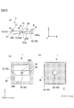
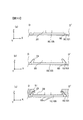
- FIGS. 1 to 3 schematically show an example of a photocoupler 1 which is a semiconductor device according to a first embodiment of the present invention.
- 1 (a) is a top perspective view
- FIG. 1 (b) is a top perspective view with the resin removed from FIG. 1 (a)
- FIG. 2 (a) is AA 'and B in FIG. 1 (a)
- 2B is a top plan view
- FIG. 2C is a back plan view.
- FIG. 3 is a perspective view of a light receiving chip to be described later.
- the photocoupler 1 As an example of the semiconductor device.
- the semiconductor device is not limited to the photocoupler 1 and may be a photomicro sensor or a mark sensor.
- the photocoupler 1 is a flat-type photocoupler in which a light emitting chip 30 having a light emitting element and a light receiving chip 20 having a light receiving element are integrally configured.
- both the light emitting surface of the light emitting element and the light receiving surface of the light receiving element are the upper surfaces (the Z axis direction + side).
- the photocoupler 1 of the present embodiment is suitable for an optical encoder, and light emitted from the light emitting element is emitted in the vertical direction of the reflection surface, that is, substantially parallel to the Z-axis direction.
- the object to be measured (not shown) is disposed outside the photocoupler 1 in the Z-axis direction, and the photocoupler 1 is configured to receive light reflected from the object to be measured by the light receiving element. .
- the photocoupler 1 includes a substrate 10, a light emitting chip 30, a light receiving chip 20, a lead terminal 101, and a resin 51.
- the light receiving chip 20 has a large number of light receiving elements (photodiodes: PD) inside, and has a rectangular shape in top view.
- the light receiving chip 20 may be configured as a phototransistor in which a PD and a transistor are combined, or may be configured as a PD and a PDIC including an integrated circuit that constitutes the PD driving circuit.
- a hole 201 is formed in a predetermined area including the center of the upper surface of the light receiving chip 20.
- the central recess 103 of the substrate 10 described later is accommodated in the hole 201 (see FIG. 2).
- the light receiving chip 20 includes the hole 201, and a thin connection portion 202 (see FIG. 3) is formed in a region along the X-axis direction in the drawing.
- the light receiving chip 20 includes a first light receiving unit 203 (Y axis direction + side in the figure) and a second light receiving unit 204 (Y axis direction-side in the figure) with the connection portion 202 interposed therebetween.
- the upper surface (the surface on the Z axis direction + side) of the connection portion 202 is formed to be recessed from the upper surface of the first light receiving unit 203 and the upper surface of the second light receiving unit 204. That is, the upper surface of the connection portion 202 is disposed at a position lower than the upper surface of the first light receiving portion 203 and the upper surface of the second light receiving portion 204 on the Z axis direction + side.
- the substrate 10 is formed of, for example, a lead frame or the like, and has a central portion 102 provided above the connection portion 202 of the light receiving chip 20 described above.
- a central recess (a light emitting element accommodating portion) 103 is formed corresponding to the area in which the hole 201 of the light receiving chip 20 is formed.
- the central recess 103 is accommodated in the hole 201 of the light receiving chip 20.
- the lead terminals 101 are arranged along the outer periphery of the first light receiving unit 203 and the second light receiving unit 204 of the light receiving chip 20.
- the lead terminal 101 is initially formed integrally with the substrate 10 as a lead frame, and is formed separately from the substrate 10 by cutting a lead portion which is a connection portion with the lead frame.
- the upper surface (the surface on the Z axis direction + side) of the central portion 102 is substantially flush with the upper surface of the first light receiving unit 203 and the upper surface of the second light receiving unit 204.
- the first light receiving unit 203 and the second light receiving unit 204 of the light receiving chip 20 are connected to the lead terminal 101 by the bonding wire 21.
- the central recess 103 is formed so that the bottom surface 103 a of the recess of the central recess 103 of the substrate 10 is at a position lower than the upper surface of the central portion 102 (in the Z axis direction in the figure).
- a light emitting chip 30 is provided on the bottom surface 103 a of the central recess 103.
- the light emitting chip 30 has a light emitting element, and is provided on the bottom surface 103 a of the central recess 103 formed in the central portion 102 of the substrate 10 described above.
- the light emitting chip 30 is electrically bonded to the substrate 10 by a conductive bonding agent such as silver paste or solder, for example.
- a conductive bonding agent such as silver paste or solder, for example.
- one electrode of the light emitting chip 30, for example, the cathode electrode is connected to the substrate 10.
- the upper surface of the light emitting chip 30, ie, the light emitting surface, and the upper surface of the light receiving chip 20, ie, the light receiving surface are aligned at substantially the same height, ie, substantially the same position in the Z-axis direction.
- the difference in height between the light emitting surface of the light emitting chip 30 and the light receiving surface of the light receiving chip 20 is preferably in the range of 30 ⁇ m or less, and more preferably in the range of 10 ⁇ m or less.
- the difference in the position in the Z-axis direction between the upper surface of the light emitting chip 30 and the upper surface of the light receiving chip 20 is substantially the same in the range of 30 ⁇ m or less.
- the central recess 103 is formed such that the bottom surface 103 a of the central recess 103 of the substrate 10 is lower than the upper surface of the central portion 102 by the size of the light emitting chip 30 in the Z axis direction.
- the other electrode of the light emitting chip 30, for example, the anode electrode is connected to the light receiving chip 20 (the first light receiving unit 203 in the example shown in the figure) by the bonding wire 31.
- the central portion 102 of the substrate 10 has a recess 102a on the lower surface side, that is, on the ⁇ Z-axis direction side.
- the connection portion 202 of the light receiving chip 20 is accommodated in the concave portion 102 a of the central portion 102 of the substrate 10.
- the connection portion 202 of the light receiving chip 20 is sealed by the resin 41 in a state of being accommodated in the concave portion 120 a of the central portion 102 of the substrate 10.
- the peripheral part of the light receiving chip 20 and a part of the lead terminal 101 in the peripheral part of the substrate 10 that is, the part excluding the back surface (Z-axis side)
- the bonding wire 21 is sealed by the resin 51.
- the resin 41 and the resin 51 are opaque resins having a light shielding property, such as epoxy.
- FIGS. 4 and 5 are sectional views taken along the line AA 'and the line BB' in FIG. 1 (a), similarly to FIG. 2 (a), and also in this case, the region of the section A'-B is shown Is omitted.
- the base material for forming the substrate 10 has such a size that a plurality of photocouplers 1 can be obtained, but in the drawing, only the region to be one photocoupler 1 and the periphery thereof are shown.
- the light receiving chip 20 is attached such that the connection portion 202 is disposed in the recess 102 a of the central portion 102 of the substrate 10. At this time, a gap g is formed between the recess 102 a of the central portion 102 of the substrate 10 and the surface on the Z axis direction ⁇ side with the surface on the Z axis direction + side of the connection portion of the light receiving chip 20. As such, it is set in advance.
- a thick plate-shaped base material capable of forming the central recess 103 is prepared in advance, and a part of the base material is removed by etching or the like to form the recess 102a and the central recess 103. deep. Further, in this state, central portion 102 of substrate 10 and the plurality of lead terminals 101 are integrally formed as a lead frame (not shown) having a frame portion on the outer periphery of substrate 10. The lead terminal 101 is connected to the lead frame by a lead portion 102 b formed on the lead frame.
- a resin 41 is sealed so as to cover the light receiving chip 20 and the substrate 10.
- the connection portion 202 of the light receiving chip 20 is made of resin filled in the concave portion 102 a provided in the central portion 102 of the substrate 10, including the gap portion with the central portion 102 of the substrate 10. Be sealed.
- the support base 60 is peeled off and removed to obtain an intermediate product 1A (FIG. 4 (b)). Depending on the metal used for the support base 60, it may be dissolved and removed.
- the up-down direction of the intermediate product 1A is reversed, and the light receiving chip 20 and the lead terminal 101 are bonded by the bonding wire 21 (FIG. 4C).
- the light emitting chip 30 is connected on the bottom surface 103a of the central recess 103 formed in the central portion 102 of the substrate 10 by die bonding using an adhesive such as silver paste (FIG. 5A).
- the electrodes of the light emitting chip 30 and the electrodes of the light receiving chip 20 are bonded by bonding wires 31 (FIG. 5 (b)).
- bonding wires 31 FIG. 5 (b)
- the photocoupler 1 includes the light receiving chip 20 in which the hole 201 is formed in a predetermined area, the light emitting chip 30 provided in the central recess 103 of the lead frame, and the resin 51 covering the peripheral portion of the light receiving chip 20 And the surface of the light receiving chip 20 and the surface of the light emitting chip 30 are substantially coplanar. Thereby, the moving distance until the light emitted from the light emitting chip 30 is reflected by the object and the moving distance until the light reflected by the object is incident to the light receiving chip 20 can be made substantially equal. Thereby, detection accuracy is improved, and high sensitivity of the sensor can be achieved.
- the photocoupler 1 can be made smaller and thinner. it can.
- the angle between the side surface and the bottom surface of the hole formed in the main surface of the transistor is determined to a predetermined value, and the light reflected by the side surface is also The light is received by the light receiving element.
- the light receiving element is formed of silicon, and the light emitting element accommodation hole of the light receiving element is formed by anisotropic etching of silicon.
- tilt angle which the circumferential side which becomes a reflective surface makes with respect to a bottom is set to 53.7 degrees and a predetermined angle, it is difficult to use except for a specific use, and versatility is low.
- the light reflected by the side surface of the structure is not received by the light receiving chip 20, it can be used for purposes other than specific applications, and a semiconductor device with high versatility can be obtained. It becomes possible to offer.
- the substrate 10 has a central recess 103 which is a light emitting element accommodating portion in which the light emitting chip 30 is provided, and the central recess 103 is disposed in the hole 201 of the light receiving chip 20.
- the light receiving chip 20 is thinner than the first light receiving unit 203 and the second light receiving unit 204 by connecting the first light receiving unit 203 and the second light receiving unit 204, and the first light receiving unit 203 and the second light receiving unit 204.
- the hole 201 is provided in the connection portion 202.
- the light emitting chip 30 can be provided on the substrate 10 in a state where the surface of the light receiving chip 20 and the surface of the light emitting chip 30 are substantially positioned on the same plane. Can be realized.
- the substrate 10 has a recess 102 a for receiving the connection portion 202 of the light receiving chip 20, and the resin 41 is filled in the recess 102 a in which the connection portion 202 is received.
- the resin 41 is also filled in the gap g between the substrate 10 and the light receiving chip 20. Thereby, high impact property can be obtained.
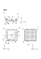
- FIG. 6 is a diagram illustrating the photocoupler 1 according to the second embodiment of the present invention
- FIG. 6 (a) is a cross-sectional view
- FIG. 6 (b) is a top plan view
- FIG. It is a top view.
- 6 (a) is a cross-sectional view taken along the line CC 'in FIG. 6 (b).
- the light receiving chip 20 has a rectangular shape in top view, and a hole 201 is formed in a predetermined area including the center.
- the light receiving chip 20 is connected to a peripheral portion of the photocoupler 1 by a plurality of lead terminals 101 formed of a lead frame or the like by bonding wires 21.
- the light emitting chip 30 is provided in the hole 201. Thereby, the upper surface of the light emitting chip 30, ie, the light emitting surface, and the upper surface of the light receiving chip 20, ie, the light receiving surface, are aligned at substantially the same height, ie, substantially the same position in the Z-axis direction.
- the height difference between the light emitting surface of the light emitting chip 30 and the light receiving surface of the light receiving chip 20 is preferably in the range of 30 ⁇ m or less, more preferably 10 ⁇ m. It shall be in the following range. In the present embodiment, in particular, the difference in height between the light emitting surface of the light emitting chip 30 and the light receiving surface of the light receiving chip 20 can be in the range of several ⁇ m or less.
- the light emitting chip 30 is connected to the light receiving chip 20 by the bonding wire 31 and connected to the lead terminal 101 by the bonding wire 32. Thereby, one electrode of the light emitting chip 30, for example, the cathode electrode is electrically connected to the lead terminal 101, and the other electrode, for example, the anode electrode is electrically connected to the light receiving chip 20.
- the light emitting chip 30 is provided in the hole 201 of the light receiving chip 20, the light receiving chip 20 and a part of the lead terminal 101 (that is, the part excluding the back surface (the surface on the Z axis ⁇ side)) Is sealed by the resin 41 at the lower portion (the Z-axis direction side) of the photocoupler 1.
- the peripheral portion of the light receiving chip 20, the lead terminal 101, and the bonding wire 21 are sealed with a resin 51 at the upper portion (Z-axis direction + side) of the photocoupler 1.
- the resin 41 and the resin 51 are opaque resins having a light shielding property, such as epoxy.
- FIGS. 7 and 8 are cross-sectional views taken along the line CC 'in FIG. 6 (b), similarly to FIG. 6 (a).
- a plurality of lead terminals 101, a light receiving chip 20, and a light emitting chip 30 are mounted on a supporting base 60.
- the base material forming the lead terminal 101 has a size such that a plurality of photocouplers 1 can be obtained, the drawing shows only a region to be one photocoupler 1 and the periphery thereof .
- the light emitting chip 30 is mounted on the support base 60 through the hole 201 formed in the light receiving chip 20.
- the plurality of lead terminals 101 are integrally formed as a lead frame (not shown) having a frame portion on the outer periphery, and each lead terminal 101 is a lead portion 102 b formed on the lead frame. Are connected to the lead frame.
- the light emitting chip 30 and the lead terminal 101 are bonded by the bonding wire 32 (FIG. 7B). Seal with resin 41 so as to cover the light receiving chip 20 and a part of the lead terminal 101 (that is, the part except the back surface (the surface on the Z-axis direction side)), the light emitting chip 30 and the bonding wire 32.
- the support substrate 60 is peeled off and removed to obtain an intermediate product 1A (FIG. 7 (c)).
- the up-down direction of the intermediate product 1A is reversed, and the light receiving chip 20 and the lead terminal 101 are bonded by the bonding wire 21 (FIG. 8A).
- the following operation and effect can be obtained.
- the light receiving chip 20, the light emitting chip 30, a part of the lead terminal 101, and the bonding wire 32 are sealed by the resin 41 from the back surface.
- the resin 41 and 51 since the portions other than the top surfaces of the light receiving chip 20 and the light emitting chip 30 are covered with the resins 41 and 51, high impact resistance can be obtained.
- the lead terminal 101 since the lead terminal 101 is sealed in an L-shape by the resins 41 and 51, the lead terminal 101 can be shaped to be resistant to resin removal.
- the upper surface of the light receiving chip 20 and the upper surface of the light emitting chip 30 on the support base 60 during manufacturing, the upper surface of the light receiving chip 20 of the photocoupler 1 and the light emitting chip
- the upper surface of the substrate 30 can be positioned on the same plane with high accuracy.
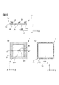
- FIG. 9 is a view illustrating the photocoupler 1 according to the third embodiment of the present invention
- FIG. 9 (a) is a cross-sectional view
- FIG. 9 (b) is a top plan view
- FIG. It is a top view.
- FIG. 9A is a cross-sectional view taken along the line DD 'in FIG. 9B.
- the light receiving chip 20 has a rectangular shape in top view, and a hole 201 is formed in a predetermined area including the center.
- the light receiving chip 20 and the light emitting chip 30 are attached to the substrate 10.
- the light emitting chip 30 is attached to the substrate 10 through the hole 201 formed in the light receiving chip 20.
- the light emitting chip 30 is bonded to the substrate 10 with a conductive bonding agent such as silver paste or solder, for example, so that one electrode (for example, the cathode electrode) is electrically connected to the substrate 10.
- the upper surface or light emitting surface of the light emitting chip 30 and the upper surface or light receiving surface of the light receiving chip 20 are aligned at substantially the same height, ie, substantially the same position in the Z-axis direction.
- the difference in height between the light emitting surface of the light emitting chip 30 and the light receiving surface of the light receiving chip 20 is preferably in the range of 30 ⁇ m or less, more preferably 10 ⁇ m. It shall be in the following range.
- the other electrode of the light emitting chip 30, for example, an anode electrode is connected to the light receiving chip 20 by a bonding wire 31.
- the substrate 10 is formed of, for example, a lead frame, and has the mounting portion 105 to which the light receiving chip 20 and the light emitting chip 30 are attached as described above, and a plurality of lead terminals 101 provided on the peripheral portion.
- the lead terminal 101 and the light receiving chip 20 are connected by a bonding wire 21.
- the photocoupler 1 and the peripheral portion of the light receiving chip 20 and the substrate 10 (that is, a part of the attachment portion 105 and a part of the lead terminal 101 (that is, a part except the back surface (Z-axis side))) Is sealed by the resin 51 in the upper part (Z-axis direction + side) of
- the resin 51 is an opaque resin having a light shielding property, such as epoxy.
- FIGS. 10 and 11 are cross-sectional views taken along the line DD 'in FIG. 9 (b), as in FIG. 9 (a).
- the substrate 10 on which a plurality of lead terminals 101 and mounting portions 105 are formed is mounted on a supporting base 60.
- the base material for forming the substrate 10 has such a size that a plurality of photocouplers 1 can be obtained, but in the drawing, only the region to be one photocoupler 1 and the periphery thereof are shown.
- the light receiving chip 20 is connected onto the mounting portion 105 of the substrate 10 by die bonding using an adhesive such as silver paste, for example.
- the light receiving chip 20 and the lead terminal 101 are connected by bonding with the bonding wire 21 (FIG. 10 (b)).
- the resin 51 is sealed so as to cover the light receiving chip 20, the peripheral portion of the substrate 10, and the bonding wire 21, and after the resin 51 is cured, the support base 60 is peeled off and removed (FIG. 10C).
- the light emitting chip 30 is connected to the mounting portion 105 of the substrate 10 by die bonding using an adhesive such as silver paste, through the hole 201 formed in the light receiving chip 20 (FIG. 11A).
- the electrodes of the light emitting chip 30 and the electrodes of the light receiving chip 20 are bonded by bonding wires 31 (FIG. 11A). Thereafter, the resin 51 is cut into pieces at the positions indicated by the one-dot chain lines in FIG. Thereby, the photocoupler 1 shown in FIG. 9 is obtained.
- the substrate 10 has a mounting portion 105 for holding the light receiving chip 20 and the light emitting chip 30. Thereby, since the light emitting chip 30 can be provided on the substrate 10, the heat dissipation can be improved.
Landscapes
- Photo Coupler, Interrupter, Optical-To-Optical Conversion Devices (AREA)
- Mechanical Treatment Of Semiconductor (AREA)
- Bipolar Transistors (AREA)
- Noodles (AREA)
Priority Applications (3)
| Application Number | Priority Date | Filing Date | Title |
|---|---|---|---|
| KR1020207018716A KR102459822B1 (ko) | 2018-01-29 | 2018-12-21 | 반도체 장치 |
| CN201880087698.1A CN111656540B (zh) | 2018-01-29 | 2018-12-21 | 半导体装置 |
| TW108103065A TWI785195B (zh) | 2018-01-29 | 2019-01-28 | 半導體裝置 |
Applications Claiming Priority (2)
| Application Number | Priority Date | Filing Date | Title |
|---|---|---|---|
| JP2018-012842 | 2018-01-29 | ||
| JP2018012842A JP6620176B2 (ja) | 2018-01-29 | 2018-01-29 | 半導体装置 |
Publications (1)
| Publication Number | Publication Date |
|---|---|
| WO2019146339A1 true WO2019146339A1 (ja) | 2019-08-01 |
Family
ID=67395853
Family Applications (1)
| Application Number | Title | Priority Date | Filing Date |
|---|---|---|---|
| PCT/JP2018/047287 Ceased WO2019146339A1 (ja) | 2018-01-29 | 2018-12-21 | 半導体装置 |
Country Status (5)
| Country | Link |
|---|---|
| JP (1) | JP6620176B2 (enExample) |
| KR (1) | KR102459822B1 (enExample) |
| CN (1) | CN111656540B (enExample) |
| TW (1) | TWI785195B (enExample) |
| WO (1) | WO2019146339A1 (enExample) |
Cited By (1)
| Publication number | Priority date | Publication date | Assignee | Title |
|---|---|---|---|---|
| WO2022219909A1 (ja) * | 2021-04-16 | 2022-10-20 | アオイ電子株式会社 | 半導体装置およびその製造方法 |
Citations (7)
| Publication number | Priority date | Publication date | Assignee | Title |
|---|---|---|---|---|
| JPS6132535A (ja) * | 1984-07-25 | 1986-02-15 | Sanyo Electric Co Ltd | センサの製造方法 |
| JPH06204508A (ja) * | 1992-12-28 | 1994-07-22 | Canon Inc | 光学式検出装置 |
| JPH1139088A (ja) * | 1997-07-16 | 1999-02-12 | Sharp Corp | 光学式入力装置 |
| JP2003004487A (ja) * | 2001-06-15 | 2003-01-08 | Olympus Optical Co Ltd | 光学式検出装置 |
| JP2005043192A (ja) * | 2003-07-28 | 2005-02-17 | Olympus Corp | 光学式エンコーダ及びその製造方法並びに光学レンズモジュール |
| JP2005283457A (ja) * | 2004-03-30 | 2005-10-13 | Olympus Corp | 光学式エンコーダ及びその製造方法 |
| US20150097111A1 (en) * | 2013-10-09 | 2015-04-09 | Sick Stegmann Gmbh | Optoelectronic sensor and method for the production of such |
Family Cites Families (11)
| Publication number | Priority date | Publication date | Assignee | Title |
|---|---|---|---|---|
| JP3684823B2 (ja) * | 1998-03-26 | 2005-08-17 | 松下電工株式会社 | 半導体リレー |
| JP3819664B2 (ja) * | 2000-03-08 | 2006-09-13 | シャープ株式会社 | 光結合素子 |
| EP1376960A1 (en) | 2002-06-29 | 2004-01-02 | Deutsche Thomson-Brandt Gmbh | Data link layer device with two transmission modes for a serial communication bus |
| JP2004063764A (ja) * | 2002-07-29 | 2004-02-26 | Toshiba Corp | 光結合半導体装置、およびその製造方法 |
| JP2005038956A (ja) * | 2003-07-17 | 2005-02-10 | Matsushita Electric Ind Co Ltd | 光部品とその製造方法 |
| JP5381280B2 (ja) * | 2009-04-23 | 2014-01-08 | オムロン株式会社 | 光結合装置 |
| KR101069197B1 (ko) * | 2009-09-25 | 2011-09-30 | 전자부품연구원 | 발광 및 수광 소자가 일체로 형성된 패키지 모듈 |
| WO2013190871A1 (ja) * | 2012-06-20 | 2013-12-27 | アオイ電子株式会社 | 光源一体型光センサ |
| JP2015095584A (ja) * | 2013-11-13 | 2015-05-18 | ローム株式会社 | 光学装置、光学装置の製造方法 |
| JP2015177052A (ja) * | 2014-03-14 | 2015-10-05 | 株式会社東芝 | 光結合装置 |
| KR102455919B1 (ko) * | 2014-07-25 | 2022-10-17 | 에이엠에스 센서스 싱가포르 피티이. 리미티드. | 서로 광학적으로 분리된 영역들을 갖는 이미지 센서를 포함하는 광전 모듈들 |
-
2018
- 2018-01-29 JP JP2018012842A patent/JP6620176B2/ja active Active
- 2018-12-21 KR KR1020207018716A patent/KR102459822B1/ko active Active
- 2018-12-21 WO PCT/JP2018/047287 patent/WO2019146339A1/ja not_active Ceased
- 2018-12-21 CN CN201880087698.1A patent/CN111656540B/zh active Active
-
2019
- 2019-01-28 TW TW108103065A patent/TWI785195B/zh active
Patent Citations (7)
| Publication number | Priority date | Publication date | Assignee | Title |
|---|---|---|---|---|
| JPS6132535A (ja) * | 1984-07-25 | 1986-02-15 | Sanyo Electric Co Ltd | センサの製造方法 |
| JPH06204508A (ja) * | 1992-12-28 | 1994-07-22 | Canon Inc | 光学式検出装置 |
| JPH1139088A (ja) * | 1997-07-16 | 1999-02-12 | Sharp Corp | 光学式入力装置 |
| JP2003004487A (ja) * | 2001-06-15 | 2003-01-08 | Olympus Optical Co Ltd | 光学式検出装置 |
| JP2005043192A (ja) * | 2003-07-28 | 2005-02-17 | Olympus Corp | 光学式エンコーダ及びその製造方法並びに光学レンズモジュール |
| JP2005283457A (ja) * | 2004-03-30 | 2005-10-13 | Olympus Corp | 光学式エンコーダ及びその製造方法 |
| US20150097111A1 (en) * | 2013-10-09 | 2015-04-09 | Sick Stegmann Gmbh | Optoelectronic sensor and method for the production of such |
Cited By (3)
| Publication number | Priority date | Publication date | Assignee | Title |
|---|---|---|---|---|
| WO2022219909A1 (ja) * | 2021-04-16 | 2022-10-20 | アオイ電子株式会社 | 半導体装置およびその製造方法 |
| JP2022164132A (ja) * | 2021-04-16 | 2022-10-27 | アオイ電子株式会社 | 半導体装置およびその製造方法 |
| JP7189994B2 (ja) | 2021-04-16 | 2022-12-14 | アオイ電子株式会社 | 半導体装置およびその製造方法 |
Also Published As
| Publication number | Publication date |
|---|---|
| KR20200090239A (ko) | 2020-07-28 |
| TW201941447A (zh) | 2019-10-16 |
| CN111656540A (zh) | 2020-09-11 |
| JP2019133994A (ja) | 2019-08-08 |
| CN111656540B (zh) | 2023-06-13 |
| JP6620176B2 (ja) | 2019-12-11 |
| KR102459822B1 (ko) | 2022-10-26 |
| TWI785195B (zh) | 2022-12-01 |
Similar Documents
| Publication | Publication Date | Title |
|---|---|---|
| KR101132071B1 (ko) | 고체 촬상 장치의 제조 방법 | |
| TWI542037B (zh) | 具有成側向形態或頂向形態裝置定向之疊層無引線載架封裝的光電子裝置 | |
| US7273765B2 (en) | Solid-state imaging device and method for producing the same | |
| CN101569023A (zh) | 用于光电子器件的壳体和光电子器件在壳体中的布置 | |
| JP2005531152A (ja) | 表面実装可能な小型発光ダイオードおよび/またはフォトダイオードおよび該ダイオードを製造するための方法 | |
| CN103797580A (zh) | 用于制造多个光电子器件的方法和光电子器件 | |
| TW202135412A (zh) | 雷射封裝結構 | |
| US20070278483A1 (en) | Light emitting device and method of manufacturing the same | |
| JP7610654B2 (ja) | 電子素子実装用基板、電子装置、および電子モジュール | |
| JP7652638B2 (ja) | 半導体装置、その製造方法および基板 | |
| WO2019146339A1 (ja) | 半導体装置 | |
| JP2005332983A (ja) | 光半導体パッケージ及びその製造方法 | |
| JP3869575B2 (ja) | 半導体レーザ | |
| US10680033B2 (en) | Chip packaging method and chip package | |
| WO2006008883A1 (ja) | 反射形光学式検出器 | |
| JP7189994B2 (ja) | 半導体装置およびその製造方法 | |
| CN100461380C (zh) | 固态成像装置及其制造方法 | |
| JPS60153184A (ja) | 受光素子 | |
| JP2004273690A (ja) | 極小光源用led素子およびその製造方法 | |
| JPS58199573A (ja) | 半導体装置 | |
| JP6485518B2 (ja) | 半導体発光装置およびその製造方法 | |
| CN218918900U (zh) | 一种光学传感器封装结构 | |
| JP2025062763A (ja) | 反射型光半導体装置およびその製造方法 | |
| JP2025103187A (ja) | 光センサ | |
| JP2025062762A (ja) | 反射型光半導体装置 |
Legal Events
| Date | Code | Title | Description |
|---|---|---|---|
| 121 | Ep: the epo has been informed by wipo that ep was designated in this application |
Ref document number: 18902429 Country of ref document: EP Kind code of ref document: A1 |
|
| ENP | Entry into the national phase |
Ref document number: 20207018716 Country of ref document: KR Kind code of ref document: A |
|
| NENP | Non-entry into the national phase |
Ref country code: DE |
|
| 122 | Ep: pct application non-entry in european phase |
Ref document number: 18902429 Country of ref document: EP Kind code of ref document: A1 |