WO2019138909A1 - 半導体レーザ装置 - Google Patents
半導体レーザ装置 Download PDFInfo
- Publication number
- WO2019138909A1 WO2019138909A1 PCT/JP2018/048181 JP2018048181W WO2019138909A1 WO 2019138909 A1 WO2019138909 A1 WO 2019138909A1 JP 2018048181 W JP2018048181 W JP 2018048181W WO 2019138909 A1 WO2019138909 A1 WO 2019138909A1
- Authority
- WO
- WIPO (PCT)
- Prior art keywords
- semiconductor laser
- laser device
- portions
- mounting
- mounting surface
- Prior art date
- Legal status (The legal status is an assumption and is not a legal conclusion. Google has not performed a legal analysis and makes no representation as to the accuracy of the status listed.)
- Ceased
Links
Images



















Classifications
-
- H—ELECTRICITY
- H01—ELECTRIC ELEMENTS
- H01S—DEVICES USING THE PROCESS OF LIGHT AMPLIFICATION BY STIMULATED EMISSION OF RADIATION [LASER] TO AMPLIFY OR GENERATE LIGHT; DEVICES USING STIMULATED EMISSION OF ELECTROMAGNETIC RADIATION IN WAVE RANGES OTHER THAN OPTICAL
- H01S5/00—Semiconductor lasers
- H01S5/40—Arrangement of two or more semiconductor lasers, not provided for in groups H01S5/02 - H01S5/30
- H01S5/4025—Array arrangements, e.g. constituted by discrete laser diodes or laser bar
- H01S5/4031—Edge-emitting structures
-
- H—ELECTRICITY
- H01—ELECTRIC ELEMENTS
- H01S—DEVICES USING THE PROCESS OF LIGHT AMPLIFICATION BY STIMULATED EMISSION OF RADIATION [LASER] TO AMPLIFY OR GENERATE LIGHT; DEVICES USING STIMULATED EMISSION OF ELECTROMAGNETIC RADIATION IN WAVE RANGES OTHER THAN OPTICAL
- H01S5/00—Semiconductor lasers
- H01S5/02—Structural details or components not essential to laser action
- H01S5/022—Mountings; Housings
- H01S5/0233—Mounting configuration of laser chips
- H01S5/02345—Wire-bonding
-
- H—ELECTRICITY
- H01—ELECTRIC ELEMENTS
- H01S—DEVICES USING THE PROCESS OF LIGHT AMPLIFICATION BY STIMULATED EMISSION OF RADIATION [LASER] TO AMPLIFY OR GENERATE LIGHT; DEVICES USING STIMULATED EMISSION OF ELECTROMAGNETIC RADIATION IN WAVE RANGES OTHER THAN OPTICAL
- H01S5/00—Semiconductor lasers
- H01S5/02—Structural details or components not essential to laser action
-
- H—ELECTRICITY
- H01—ELECTRIC ELEMENTS
- H01S—DEVICES USING THE PROCESS OF LIGHT AMPLIFICATION BY STIMULATED EMISSION OF RADIATION [LASER] TO AMPLIFY OR GENERATE LIGHT; DEVICES USING STIMULATED EMISSION OF ELECTROMAGNETIC RADIATION IN WAVE RANGES OTHER THAN OPTICAL
- H01S5/00—Semiconductor lasers
- H01S5/02—Structural details or components not essential to laser action
- H01S5/022—Mountings; Housings
- H01S5/023—Mount members, e.g. sub-mount members
- H01S5/0232—Lead-frames
-
- H—ELECTRICITY
- H01—ELECTRIC ELEMENTS
- H01S—DEVICES USING THE PROCESS OF LIGHT AMPLIFICATION BY STIMULATED EMISSION OF RADIATION [LASER] TO AMPLIFY OR GENERATE LIGHT; DEVICES USING STIMULATED EMISSION OF ELECTROMAGNETIC RADIATION IN WAVE RANGES OTHER THAN OPTICAL
- H01S5/00—Semiconductor lasers
- H01S5/02—Structural details or components not essential to laser action
- H01S5/022—Mountings; Housings
- H01S5/023—Mount members, e.g. sub-mount members
- H01S5/02325—Mechanically integrated components on mount members or optical micro-benches
- H01S5/02326—Arrangements for relative positioning of laser diodes and optical components, e.g. grooves in the mount to fix optical fibres or lenses
-
- H—ELECTRICITY
- H01—ELECTRIC ELEMENTS
- H01S—DEVICES USING THE PROCESS OF LIGHT AMPLIFICATION BY STIMULATED EMISSION OF RADIATION [LASER] TO AMPLIFY OR GENERATE LIGHT; DEVICES USING STIMULATED EMISSION OF ELECTROMAGNETIC RADIATION IN WAVE RANGES OTHER THAN OPTICAL
- H01S5/00—Semiconductor lasers
- H01S5/02—Structural details or components not essential to laser action
- H01S5/026—Monolithically integrated components, e.g. waveguides, monitoring photo-detectors, drivers
-
- H—ELECTRICITY
- H01—ELECTRIC ELEMENTS
- H01S—DEVICES USING THE PROCESS OF LIGHT AMPLIFICATION BY STIMULATED EMISSION OF RADIATION [LASER] TO AMPLIFY OR GENERATE LIGHT; DEVICES USING STIMULATED EMISSION OF ELECTROMAGNETIC RADIATION IN WAVE RANGES OTHER THAN OPTICAL
- H01S5/00—Semiconductor lasers
- H01S5/02—Structural details or components not essential to laser action
- H01S5/022—Mountings; Housings
-
- H—ELECTRICITY
- H01—ELECTRIC ELEMENTS
- H01S—DEVICES USING THE PROCESS OF LIGHT AMPLIFICATION BY STIMULATED EMISSION OF RADIATION [LASER] TO AMPLIFY OR GENERATE LIGHT; DEVICES USING STIMULATED EMISSION OF ELECTROMAGNETIC RADIATION IN WAVE RANGES OTHER THAN OPTICAL
- H01S5/00—Semiconductor lasers
- H01S5/02—Structural details or components not essential to laser action
- H01S5/022—Mountings; Housings
- H01S5/02208—Mountings; Housings characterised by the shape of the housings
-
- H—ELECTRICITY
- H01—ELECTRIC ELEMENTS
- H01S—DEVICES USING THE PROCESS OF LIGHT AMPLIFICATION BY STIMULATED EMISSION OF RADIATION [LASER] TO AMPLIFY OR GENERATE LIGHT; DEVICES USING STIMULATED EMISSION OF ELECTROMAGNETIC RADIATION IN WAVE RANGES OTHER THAN OPTICAL
- H01S5/00—Semiconductor lasers
- H01S5/02—Structural details or components not essential to laser action
- H01S5/022—Mountings; Housings
- H01S5/02218—Material of the housings; Filling of the housings
- H01S5/0222—Gas-filled housings
-
- H—ELECTRICITY
- H01—ELECTRIC ELEMENTS
- H01S—DEVICES USING THE PROCESS OF LIGHT AMPLIFICATION BY STIMULATED EMISSION OF RADIATION [LASER] TO AMPLIFY OR GENERATE LIGHT; DEVICES USING STIMULATED EMISSION OF ELECTROMAGNETIC RADIATION IN WAVE RANGES OTHER THAN OPTICAL
- H01S5/00—Semiconductor lasers
- H01S5/02—Structural details or components not essential to laser action
- H01S5/022—Mountings; Housings
- H01S5/023—Mount members, e.g. sub-mount members
- H01S5/0231—Stems
Definitions
- the present disclosure relates to a semiconductor laser device.
- Semiconductor laser devices are widely used as light source devices for various electronic devices.
- Japanese Patent Application Laid-Open No. 201-147301 discloses an example of a conventional semiconductor laser device.
- the semiconductor laser device disclosed in the document includes a disk-shaped base portion and a heat sink portion provided on the upper surface of the base portion.
- a semiconductor laser element is mounted on the heat sink portion.
- Two leads extend from the lower surface of the base portion.
- This conventional semiconductor laser device is mounted on the circuit board in a state where the leads are inserted through the holes formed in the circuit board.
- Patent Document 1 Japanese Patent Application Publication No. 201-147301
- a surface mount semiconductor laser device may be required depending on the type of electronic device.
- An object of the present disclosure is to provide a semiconductor laser device capable of surface mounting.
- a semiconductor laser device provided by the present disclosure includes: a semiconductor laser device; a base for supporting the semiconductor laser device; and a wiring portion which is formed on the base and which forms a conduction path to the semiconductor laser device.
- the base is directed to one side in the thickness direction of the base and is opposite to the mounting surface on which the semiconductor laser device is mounted, and the semiconductor laser in a first direction perpendicular to the thickness direction.
- an emitting unit located on the side. The light from the semiconductor laser device is emitted through the emission unit.
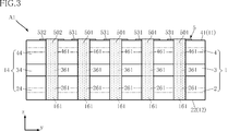
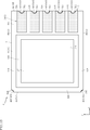
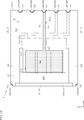
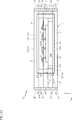
- FIG. 1 is a plan view showing a semiconductor laser device according to a first embodiment. It is a front view showing a semiconductor laser device concerning a 1st embodiment. It is a side view showing a semiconductor laser device concerning a 1st embodiment. It is a bottom view showing a semiconductor laser device concerning a 1st embodiment.
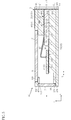
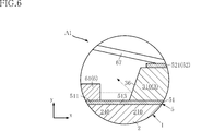
- FIG. 5 is a cross-sectional view taken along the line VV of FIG. 1; It is an expanded sectional view showing a part of semiconductor laser device concerning a 1st embodiment.
- FIG. 7 is a cross-sectional view taken along the line VII-VII in FIG. It is a top view which shows the substrate of the semiconductor laser device concerning a 1st embodiment.
- FIG. 17 is a cross-sectional view taken along the line XVII-XVII in FIG. It is a top view which shows the semiconductor laser device concerning a 2nd embodiment. It is a top view explaining the base material of the semiconductor laser device concerning a 2nd embodiment. It is a top view explaining the base material of the semiconductor laser device concerning a 2nd embodiment. It is a top view which shows the semiconductor laser device concerning a 3rd embodiment. It is a side view showing a semiconductor laser device concerning a 3rd embodiment. It is a bottom view showing a semiconductor laser device concerning a 3rd embodiment.
- FIG. 17 is a cross-sectional view taken along the line XVII-XVII in FIG. It is a top view which shows the semiconductor laser device concerning a 2nd embodiment. It is a top view explaining the base material of the semiconductor laser device concerning a 2nd embodiment. It is a top view which shows the semiconductor laser device concerning a 3rd embodiment. It is a side view showing a semiconductor laser device concerning a 3
- FIG. 22 is a cross-sectional view taken along the line XXIV-XXIV of FIG. 21. It is a top view explaining the base material of the semiconductor laser device concerning a 3rd embodiment. It is a top view explaining the base material of the semiconductor laser device concerning a 3rd embodiment. It is a top view explaining the base material of the semiconductor laser device concerning a 3rd embodiment. It is sectional drawing which shows the 1st modification of the semiconductor laser apparatus concerning 3rd Embodiment. It is a top view which shows the semiconductor laser device concerning a 4th embodiment. It is a bottom view which shows the semiconductor laser device concerning a 4th embodiment.
- FIG. 30 is a cross-sectional view taken along the line XXXI-XXXI of FIG. 29.
- FIG. 30 is a cross-sectional view taken along the line XXXII-XXXII in FIG. It is a top view which shows the semiconductor laser device concerning a 5th embodiment. It is a front view showing a semiconductor laser device concerning a 5th embodiment.
- FIG. 34 is a cross-sectional view taken along the line XXXV-XXXV in FIG. It is a top view which shows the semiconductor laser device concerning a 6th embodiment. It is a bottom view which shows the semiconductor laser device concerning a 6th embodiment.
- FIG. 37 is a cross-sectional view taken along the line XXXVIII-XXXVIII of FIG. 36. It is a top view which shows the semiconductor laser device concerning a 7th embodiment. It is a bottom view which shows the semiconductor laser device concerning a 7th embodiment.
- the semiconductor laser device A1 includes a base 1, a wiring portion 5, a semiconductor laser element 6, a plurality of through wires 69, a first cover 7 and a second cover 8.
- the z direction corresponds to the thickness direction of the substrate 1.
- the x direction corresponds to a first direction
- the y direction corresponds to a second direction.
- the upper side in the drawing corresponds to "one side”
- the lower side corresponds to "the other side”.
- the x direction it may be referred to as "front side” as corresponding to one side, and may be referred to as “rear side” as corresponding to the other side.
- these terms “one”, “another”, “front”, and “rear” are for convenience of description, and do not limit the configuration of the semiconductor laser device of the present disclosure.
- the substrate 1 supports the semiconductor laser device 6. At least the surface of the substrate 1 is made of an insulating material.
- the base material 1 has a main surface 11, a back surface 12, a front end surface 13, a rear end surface 14, a pair of side surfaces 15, an opening 17, an emission portion 18, a plurality of rear groove portions 161, plural The front groove portion 163 and the front concave portion 171 of the
- the dimensions in the x direction are about 2.0 mm to 7.0 mm
- the dimensions in the y direction are about 1.5 mm to 7.0 mm
- the dimensions in the z direction are about 0.7 mm to 2.5 mm.
- the size and shape of the substrate 1 are not limited to this example.
- the major surface 11 is a surface that faces one side (upper side) in the z direction.
- the main surface 11 corresponds to a mounting surface.
- the major surface 11 is perpendicular to the z-direction.
- the main surface 11 is substantially rectangular.
- the back surface 12 is on the opposite side of the main surface 11 and faces the other side (lower side) in the z direction. In the illustrated example, the back side 12 is perpendicular to the z-direction.
- the back surface 12 is substantially rectangular.
- the front end surface 13 is a surface facing the one side (front side) in the x direction, and connects the main surface 11 and the back surface 12. In the illustrated example, the front end face 13 is perpendicular to the x-direction.
- the pair of side surfaces 15 connect the main surface 11 and the back surface 12 and connect the front end surface 13 and the rear end surface 14.
- the pair of side surfaces 15 are separated from each other in the y direction.
- each side surface 15 is substantially rectangular and perpendicular to the y direction.
- the opening 17 is a portion that opens the internal space defined by the substrate 1 to one side (upper side) in the z direction. In the illustrated example, it has a substantially rectangular shape in the z direction (plan view) (see FIG. 10). The openings 17 are arranged to be biased to one side (front side) in the x direction. By providing the opening 17, the main surface 11 is a rectangular ring (closed frame shape) in a z-direction view.
- the emitting portion 18 is a portion for emitting the laser beam from the semiconductor laser element 6 to one side (front side) in the x direction.
- the internal space defined by the base material 1 is opened to one side (front side) in the x direction by the emission unit 18.
- the emitting unit 18 is, for example, rectangular in the x-direction (see FIG. 2).
- the front end surface 13 is rectangular annular shape in x direction view by the output part 18 being provided.
- the plurality of rear grooves 161 are recessed from the rear end surface 14 (see FIG. 1), and each extend in the z direction (see FIG. 3). Each rear groove portion 161 reaches the main surface (mounting surface) 11. In the illustrated example, each rear groove portion 161 reaches the back surface 12.
- the cross-sectional shape of the rear groove portion 161 is semicircular in the illustrated example, but the present disclosure is not limited thereto.
- the plurality of rear grooves 161 are spaced apart from one another in the y direction.
- the plurality of front grooves 163 are formed at the boundary between the pair of side surfaces 15 and the front end surface 13.
- Each front groove portion 163 extends in the z direction and reaches the main surface 11 and the back surface 12.
- the cross-sectional shape of the rear groove portion 161 is a quarter circle in the illustrated example, but the present disclosure is not limited thereto.
- the front recess 171 is recessed from the front end face 13 to the other side (rear side) in the x direction, and surrounds the periphery of the emitting portion 18.
- the front recess 171 has a rectangular ring shape in the x direction.
- the front recess 171 is a portion for providing the first cover 7.
- the substrate 1 includes a plurality of layers.
- the substrate 1 comprises a first layer 2, a second layer 3 and a third layer 4.
- the first layer 2, the second layer 3 and the third layer 4 are stacked in the z direction.
- the first layer 2, the second layer 3 and the third layer 4 are formed of, for example, a ceramic such as alumina or aluminum nitride, but the present disclosure is not limited thereto.
- Each layer itself may be composed of a plurality of ceramic layers.
- FIG. 2, FIG. 3, FIG. 5 and FIG. 7, the alternate long and short dashed lines indicate the boundaries between adjacent ceramic layers.
- the first layer 2 is located at the lowermost side in the z direction.
- the first layer 2 has a first main surface 21, a first back surface 22, a first front end surface 23, a first rear end surface 24, a pair of first side surfaces 25, a first main portion 210, a pair of first side frame portions 220, a first front frame 230, a pedestal 240, a bottom 250, a plurality of first rear grooves 261, and a plurality of first front grooves 263.
- the first major surface 21 is a surface facing the upper side in the z direction.
- the first major surface 21 corresponds to a mounting surface.
- the first major surface 21 is perpendicular to the z direction.
- the first back surface 22 is on the opposite side to the first major surface 21 and faces the lower side in the z direction. In the illustrated example, the first back surface 22 is perpendicular to the z direction. The first back surface 22 constitutes the back surface 12.
- the first front end surface 23 is a surface facing the one side (front side) in the x direction, and connects the first main surface 21 and the first back surface 22. In the illustrated example, the first front end face 23 is perpendicular to the x-direction. The first front end face 23 constitutes a part of the front end face 13.
- the first rear end surface 24 is a surface facing the other side (rear side) in the x direction, and connects the first major surface 21 and the first back surface 22.
- the first aft end face 24 is perpendicular to the x-direction.
- the first rear end face 24 constitutes a part of the rear end face 14.
- the first main portion 210 is a portion of the first layer 2 located on the rear side in the x direction. In the illustrated example, the first main portion 210 is substantially rectangular in the z direction. The thickness of the first main portion 210 is the same as the maximum thickness of the first layer 2.
- the pair of first side frame portions 220 is a portion extending from the both sides of the first main portion 210 in the y direction to the front side in the x direction.
- the thickness of the first side frame 220 is the same as the maximum thickness of the first layer 2.
- the first front frame portion 230 connects one side end of the pair of first side frame portions 220 in the x direction to one another, and extends in the y direction.
- the pair of first side frame portions 220 and the first front frame portion 230 constitute a frame-shaped portion.
- a recess 231 is formed in the first front frame portion 230.
- the concave portion 231 is a portion where the first front frame portion 230 is partially reduced in z-direction size, and constitutes a part of the front concave portion 171.
- the pedestal portion 240 extends from the first main portion 210 to one side (front side) in the x direction, and in the illustrated example, has a substantially rectangular shape in the z direction.
- the pedestal portion 240 is separated from the pair of first side frame portions 220 and the first front frame portion 230.
- the semiconductor laser element 6 is mounted on the pedestal portion 240.
- the bottom portion 250 is a portion located on the other side (lower side) in the z direction from the first major surface 21.
- the bottom portion 250 is provided in a region surrounded by the pair of first side frame portions 220, the first front frame portion 230, and the pedestal portion 240 in the z direction.
- the thickness of the bottom 250 is smaller than the maximum thickness in the z direction of the first layer 2.
- the plurality of first rear grooves 261 are recessed from the first rear end surface 24 and extend in the z direction.
- the first rear groove portion 261 reaches the first major surface 21 and the first back surface 22.
- the cross-sectional shape of the first rear groove portion 261 is not particularly limited, and in the illustrated example, it is semicircular.
- the plurality of first rear groove portions 261 are disposed apart from one another in the y direction.
- the plurality of first rear groove portions 261 configure a part of each of the plurality of rear groove portions 161.
- the plurality of first front groove portions 263 are formed at the boundary between the pair of first side surfaces 25 and the first front end surface 23.
- the first front groove portion 263 extends in the z direction, and reaches the first major surface 21 and the first back surface 22.
- the cross-sectional shape of the first front groove portion 263 is not particularly limited, and in the illustrated example, it has a quadrilateral shape.
- the plurality of first front groove portions 263 constitute a part of each of the plurality of front groove portions 163.
- the second layer 3 is stacked on one side (upper side) in the z direction of the first layer 2.
- the second layer 3 has a second main surface 31, a second back surface 32, a second front end surface 33, a second rear end surface 34, a pair of second side surfaces 35, an inner end surface 36, a second main portion 310, a pair of second Two side frame portions 320 have a plurality of second rear grooves 361 and a plurality of second front grooves 363.
- the second major surface 31 is a surface that faces one side in the z direction (upper side). In the illustrated example, the second major surface 31 is perpendicular to the z direction.
- the second back surface 32 is a surface facing the other side (lower side) in the z direction, which is the side opposite to the side to which the second main surface 31 faces, and faces the first main surface 21 of the first layer 2 .
- the second back surface 32 is perpendicular to the z direction.
- the second front end surface 33 is a surface facing the one side (front side) in the x direction, and connects the second main surface 31 and the second back surface 32.
- the second front end face 33 is perpendicular to the x-direction.
- the second front end face 33 constitutes a part of the front end face 13.
- the second front end face 33 includes two regions spaced apart on both sides in the y direction.
- the second rear end surface 34 is a surface facing the other side (rear side) in the x direction, and connects the second main surface 31 and the second rear surface 32.
- the second aft end face 34 is perpendicular to the x-direction.
- the second rear end surface 34 constitutes a part of the rear end surface 14.
- the pair of second side surfaces 35 connects the second main surface 31 and the second back surface 32, and connects the second front end surface 33 and the second rear end surface 34.
- the pair of second side surfaces 35 respectively face the y direction.
- the second side surface 35 is perpendicular to the y direction.
- the second side surface 35 constitutes a part of the side surface 15.
- the second main portion 310 is a portion of the second layer 3 located on the other side (rear side) in the x direction.
- the second main portion 310 is substantially rectangular in the z direction.
- the thickness of the second main portion 310 is the same as the maximum thickness of the second layer 3.
- the inward end surface 36 is a surface located on one side (front side) in the x direction of the second main portion 310.
- the inward end face 36 is inclined with respect to the z direction, and the z direction one side (the front side, the view, from the one side in the z direction (the upper side in the view in FIG. 6) to the other side (the lower side in the view in FIG. It inclines so that it may be located in the left in the figure in 6).
- the pair of second side frame portions 320 is a portion extending from one side of the second main portion 310 in the y direction to one side (front side) in the x direction.
- the thickness of the second side frame 320 is the same as the maximum thickness of the second layer 3.
- Recesses 321 are formed in the pair of second side frame portions 320, respectively.
- the concave portion 321 is a portion of the second side frame portion 320 which is recessed from the second front end surface 33 to the other side (rear side) in the x direction. Moreover, the recessed part 321 is located inside y direction.
- the pair of recesses 321 constitute a part of the front recess 171.
- the plurality of second rear grooves 361 are recessed from the second rear end surface 34 and extend in the z direction.
- the second rear groove 361 reaches the second major surface 31 and the second back surface 32.
- the cross-sectional shape of the second rear groove 361 is not particularly limited, and in the illustrated example, it is semicircular.
- the plurality of second rear grooves 361 are disposed apart from one another in the y direction.
- the plurality of second rear groove portions 361 constitute a part of each of the plurality of rear groove portions 161.
- the plurality of second front grooves 363 are formed at the boundary between the pair of second side surfaces 35 and the second front end surface 33.
- the second front groove portion 363 extends in the z direction, and reaches the second major surface 31 and the second back surface 32.
- the cross-sectional shape of the second front groove portion 363 is not particularly limited, and in the illustrated example, it has a quarter circle shape.
- the plurality of second front groove portions 363 configure a part of each of the plurality of front groove portions 163.
- the third layer 4 is located on the most side (upper side) in the z direction.
- the third layer 4 is stacked on one side (upper side) in the z direction of the second layer 3.
- the third layer 4 has a third main surface 41, a third back surface 42, a third front end surface 43, a third rear end surface 44, a pair of third side surfaces 45, a third main portion 410, a pair of third side frame portions
- a third front frame 430, a plurality of third rear grooves 461, and a plurality of third front grooves 463 are provided.
- the third major surface 41 is a surface facing the one side (upper side) in the z direction. In the illustrated example, the third major surface 41 is perpendicular to the z direction. In the present embodiment, the third major surface 41 constitutes the major surface 11.
- the third back surface 42 is a surface facing the other side (lower side) in the z direction, which is the opposite side to the side to which the third main surface 41 faces, and faces the second main surface 31 of the second layer 3 .
- the third back surface 42 is perpendicular to the z-direction.
- the third front end surface 43 is a surface facing the one side (front side) in the x direction, and connects the third main surface 41 and the third back surface 42. In the illustrated example, the third front end surface 43 is perpendicular to the x direction. The third front end surface 43 constitutes a part of the front end surface 13.
- the third rear end surface 44 is a surface facing the other side (rear side) in the x direction, and connects the third main surface 41 and the third back surface 42.
- the third aft end face 44 is perpendicular to the x-direction.
- the third rear end surface 44 constitutes a part of the rear end surface 14.
- the pair of third side surfaces 45 connects the third main surface 41 and the third back surface 42, and connects the third front end surface 43 and the third rear end surface 44.
- the pair of third side surfaces 45 respectively face the y direction.
- the third side 45 is perpendicular to the y direction.
- the third side surface 45 constitutes a part of the side surface 15.
- the third main portion 410 is a portion of the third layer 4 located on the other side (rear side) in the x direction.
- the third main portion 410 is substantially rectangular in z-direction.
- the thickness of the third main portion 410 is the same as the maximum thickness of the second layer 3.
- the pair of third side frame portions 420 is a portion extending from one side of the third main portion 410 in the y direction to one side (front side) in the x direction.
- the third front frame portion 430 connects one end of the pair of third side frame portions 420 in the x direction to one another, and extends in the y direction.
- the pair of third side frame portions 420 and the third front frame portion 430 form a frame-shaped portion.
- a recess 431 is formed in the third front frame 430.
- the recess 431 is a portion recessed from the third front end surface 43 to the other side (rear side) in the x direction, and constitutes a part of the front recess 171.
- the plurality of third rear grooves 461 are recessed from the third rear end surface 44 and extend in the z direction.
- the third rear groove portion 461 reaches the third major surface 41 and the third back surface 42.
- the cross-sectional shape of the third rear groove 461 is not particularly limited, and in the illustrated example, it is semicircular.
- the plurality of third rear grooves 461 are disposed apart from one another in the y direction.
- the plurality of third rear groove portions 461 configure a part of each of the plurality of rear groove portions 161.
- the plurality of third front grooves 463 are formed at the boundary between the pair of third side surfaces 45 and the third front end surface 43.
- the third front groove portion 463 extends in the z direction, and reaches the third major surface 41 and the third back surface 42.
- the cross-sectional shape of the third front groove portion 463 is not particularly limited, and in the illustrated example, it has a quadrilateral shape.
- the plurality of third front groove portions 463 configure a part of each of the plurality of front groove portions 163.
- the opening 17 is formed in the third layer 4. Further, in the third layer 4, an annular recess 440 is formed. In the annular recess 440, a portion surrounding the opening 17 in the third layer 4 is a portion recessed from the third main surface 41 (main surface 11) to the other side (lower side) in the z direction.
- the annular recess 440 has a rectangular annular shape in the z direction.
- the annular recess 440 is a portion for providing the second cover 8.
- the wiring portion 5 is formed on the base material 1 and constitutes a conduction path to the semiconductor laser element 6.
- the wiring unit 5 includes a first wiring unit 51, a second wiring unit 52, a third wiring unit 53, and a plurality of rear connection units. 501 and a plurality of front portions 505.
- the wiring portion 5 is made of a material having an appropriate conductivity, and is formed, for example, by plating or attachment.
- a material of the wiring part 5 Cu, Ni, Ti, Au etc. are selected suitably, for example.
- a surface layer made of Sn may be provided in a portion of the wiring portion 5 to which the solder is attached.
- the first wiring portion 51 is a portion formed in the first layer 2 of the base 1.
- the first wiring portion 51 includes an element mounting portion 511, a first strip portion 512, and a first connecting portion 513.
- the element mounting portion 511 is formed on the first major surface 21 of the pedestal portion 240 of the first layer 2 of the base 1.
- the element mounting portion 511 is a portion on which the semiconductor laser element 6 is mounted.
- the element mounting portion 511 has a substantially rectangular shape in the z direction, and covers most of the pedestal portion 240.
- the first strip portion 512 is formed in the first main portion 210 of the first layer 2 and reaches one of the plurality of first rear groove portions 261 that is located at the bottom of FIG. 8 in the y direction. ing. In addition, the first strip portion 512 extends from the first rear groove portion 261 along the x direction.
- the first connecting portion 513 connects the element mounting portion 511 and the first band-shaped portion 512.
- the shape and size of the first connection portion 513 are not particularly limited, and in the illustrated example, the shape has two bent portions.
- the second wiring portion 52 is a portion formed on the second layer 3 of the base 1.
- the second wiring portion 52 includes a plurality of wire bonding portions 521, a plurality of second strip portions 522, and a plurality of second connection portions 523.
- the plurality of wire bonding portions 521 are portions to which the plurality of wires 67 are connected.
- the plurality of wire bonding portions 521 are arranged in the y direction, and are formed on one side (front side) of the second main portion 310 in the x direction.
- the shape of the wire bonding portion 521 is not particularly limited, and in the illustrated example, it is rectangular. As shown in FIG. 1, the plurality of wire bonding portions 521 are exposed from the third layer 4 in the z direction.
- the plurality of second strip portions 522 are formed in the second main portion 310 of the second layer 3 and among the plurality of second rear groove portions 361, four second rear groove portions in the upper side in FIG. It has reached 361.
- the second strip 522 extends from the second rear groove 361 along the x direction.
- the first band-shaped portion 512 and the plurality of second band-shaped portions 522 are arranged separately in the y direction when viewed in the z-direction.
- the plurality of second connection portions 523 connect the plurality of wire bonding portions 521 and the plurality of second strip portions 522.
- the shape and size of the second connection portion 523 are not particularly limited, and in the illustrated example, the shape has two bent portions.
- the third wiring portion 53 is a portion formed in the third layer 4 of the base 1.
- the third wiring portion 53 has a plurality of mounting terminal portions 531 and mounting terminal portions 532.
- the plurality of mounting terminal portions 531 are formed in the third main portion 410 of the third layer 4 and arranged to be separated from each other in the y direction.
- the plurality of mounting terminal portions 531 reach the four third rear groove portions 461 in the upper side in FIG. 10 in the y direction in the plurality of third rear groove portions 461.
- the mounting terminal portion 531 extends from the third rear groove 461 along the x direction.
- the y-direction dimension of the mounting terminal portion 531 is larger than the y-direction dimension of the second strip portion 522.
- the plurality of mounting terminal portions 531 are, for example, an anode electrode.
- the mounting terminal portion 532 is formed in the third main portion 410 of the third layer 4.
- the mounting terminal portion 532 reaches one of the plurality of third rear groove portions 461 that is located on the lowermost side in FIG. 10 in the y direction. Further, the mounting terminal 532 extends from the third rear groove 461 along the x direction.
- the y-direction dimension of the mounting terminal portion 532 is larger than the y-direction dimension of the first strip portion 512.
- the plurality of mounting terminal portions 531 and the mounting terminal portions 532 are arranged separately from each other in the y direction.
- the mounting terminal 532 is, for example, a cathode electrode.
- the center O1 of the wire bonding portion 521 and the center O2 of the mounting terminal portion 531 which are conductive to each other in the z direction are displaced by the distance G in the y direction There is.
- the plurality of distances G shown in FIG. 1 may have the same size as each other or may have different sizes.
- an extension line E obtained by virtually extending the y-direction end edge of the wire bonding portion 521 intersects the mounting terminal portion 531.
- the plurality of rear communication portions 501 are formed so as to cover the four rear grooves 161 on the right side in the drawing among the plurality of rear grooves 161 of the base 1.
- the rear communication portion 501 reaches the z-direction one side end (upper side end) of the rear groove portion 161. Further, in the illustrated example, the rear communication portion 501 reaches the other end (lower end) of the rear groove portion 161 in the z direction.
- the rear connection portion 501 is in contact with the second strip portion 522 of the second wiring portion 52 and the mounting terminal portion 531 of the third wiring portion 53, and is electrically connected thereto.
- the wire bonding portion 521 is electrically connected to the mounting terminal portion 531 through the second connection portion 523, the second strip portion 522, and the rear connection portion 501.
- the rear communication portion 502 is formed to cover the rear groove portion 161 at the left end in FIG. 3 among the plurality of rear groove portions 161 of the base 1. In the present embodiment, the rear communication portion 502 reaches the z-direction one side end (upper side end) of the rear groove portion 161. Further, in the illustrated example, the rear communication portion 502 reaches the other end (lower end) of the rear groove portion 161 in the z direction.
- the rear connection portion 502 is in contact with the first strip portion 512 of the first wiring portion 51 and the mounting terminal portion 532 of the third wiring portion 53, and is electrically connected thereto. As a result, the element mounting portion 511 is electrically connected to the mounting terminal portion 532 via the first connection portion 513, the first strip portion 512, and the rear connecting portion 502.
- the plurality of front portions 505 respectively cover the plurality of front grooves 163.
- the front portion 505 covers the entire front groove portion 163 and reaches both ends of the front groove portion 163 in the z direction.
- the front portion 505 is not in contact with the first wiring portion 51, the second wiring portion 52, and the third wiring portion 53, and is not electrically connected to these portions.
- the plurality of waveguides 62 are portions that generate laser light of a predetermined wavelength by repeatedly reflecting light emitted in the active layer in the x direction.
- the plurality of waveguides 62 are arranged separately from one another in the y direction, and each extend along the x direction.
- the semiconductor laser device 6 is a multi-beam type, and can emit laser light from each waveguide 62 individually (that is, independently from the other waveguides).
- the plurality of electrodes 63 are provided corresponding to the plurality of waveguides 62 and arranged to be separated from each other in the y direction.
- a plurality of wires 67 are connected to the plurality of electrodes 63 separately. In the illustrated example, a plurality of wires 67 are connected to one electrode 63 for the purpose of passing a larger current.
- an electrode (not shown) provided on the lower surface of the semiconductor layer 61 of the semiconductor laser element 6 is conductively joined to the element mounting portion 511 by a conductive bonding material (not shown) such as Ag paste. .
- the semiconductor laser device 6 is mounted on the first major surface 21 of the pedestal portion 240.
- the one side end of the semiconductor laser device 6 in the x direction protrudes from the pedestal portion 240 by one length L in the x direction. This protrusion is preferable for suppressing interference of light from the semiconductor laser element 6 with the pedestal portion 240, and is shown as a similar configuration also in the subsequent drawings.
- one side end of the semiconductor laser device 6 in the x direction substantially matches one side end of the pedestal portion 240 in the z direction, etc.
- the semiconductor laser device 6 may not protrude from the pedestal 240.
- the number of waveguides 62 provided in the semiconductor laser device 6 is not particularly limited.
- the semiconductor laser device 6 has four waveguides 62.
- the semiconductor laser device 6 has four electrodes 63.
- the second wiring portion 52 also has four wire bonding portions 521, four second strip portions 522, and four second connection portions 523.
- the substrate 1 has five back grooves 161, and the wiring part 5 has four back communication parts 501 and one back communication part 502.
- the third wiring portion 53 has four mounting terminal portions 531 and one mounting terminal portion 532.
- the first cover 7 closes the emitting portion 18 and is made of a material that transmits the light from the semiconductor laser device 6.
- the first cover 7 is made of, for example, transparent glass.
- the first cover 7 may be provided with a predetermined coating for improving the emission efficiency.
- the first cover 7 is rectangular in the x direction, and is accommodated in the front recess 171 of the base 1.
- the attachment method to the base material 1 of the 1st cover 7 is not specifically limited, For example, it adhere
- the first cover 7 has a flat plate shape whose dimension in the x direction is uniform.
- the second cover 8 closes the opening 17.
- the material of the second cover 8 is not particularly limited, and in the present embodiment, it is made of, for example, glass. Further, the second cover 8 may be provided with a predetermined coating for attenuating a predetermined extraneous ray.
- the second cover 8 is rectangular in the z direction, and is accommodated in the annular recess 440 of the base 1.
- the attachment method to the base material 1 of the 2nd cover 8 is not specifically limited, For example, it adhere
- the internal space defined by the base 1 may be sealed by the first cover 7 and the second cover 8.
- the first cover 7 and the second cover 8 can It is preferable that it is the structure pressed on the material 1.
- a plurality of mounting terminal portions 531 and mounting terminal portions 532 are formed on the main surface 11 (third main surface 41), and the main surface 11 (third main surface 41) is used as a mounting surface. ing. Therefore, the semiconductor laser device A1 can be surface mounted on a circuit board (not shown) or the like.
- the main surface 11 is a mounting surface
- laser light can be emitted from the semiconductor laser device A1 to one side (front side) in the x direction.
- the emitting direction of the laser light can be made to differ by 90 ° with respect to the semiconductor laser device of the type mounted using the leads.
- the opening 17 is configured to open from the main surface 11 as a mounting surface.
- the opening 17 is in the posture of facing the upper side in the vertical direction.
- mounting of the semiconductor laser element 6, bonding of the wire 67, and attachment of the first cover 7 and the second cover 8 are performed.
- the conduction test and the light emission test of the semiconductor laser device 6 can be performed by using the plurality of mounting terminal portions 531 and the mounting terminal portions 532 which are in the state of turning upward in the vertical direction.
- the first major surface 21 on one side in the x direction of the pedestal portion 240 is located on the one side in the z direction from the bottom portion 250.
- the first main surface 21 as a mounting surface, it is possible to suppress that the laser light emitted from the semiconductor laser element 6 is blocked by the pedestal portion 240 and the bottom portion 250.
- the configuration in which the x direction one side end (front side end) of the semiconductor laser element 6 is protruded from the pedestal portion 240 to the x direction one side (front side) is preferable for preventing the laser light from being blocked.
- the semiconductor laser device 6 is not limited to the configuration that protrudes from the pedestal portion 240.
- the plurality of second strip portions 522 extend to the other side (rear side) in the x direction with respect to the semiconductor laser device 6. That is, the plurality of second band-shaped portions 522 are provided on the side opposite to the side from which the laser light of the semiconductor laser element 6 is emitted. Thereby, it is possible to make the plurality of second band-shaped portions 522 linear, and to be arranged so that their distances do not differ significantly. This is suitable for equalizing the path lengths of the conduction paths to the plurality of waveguides 62 and the plurality of electrodes 63 of the semiconductor laser device 6.
- first band-like portions 512 are linear as in the case of the plurality of second band-like portions 522, and are arranged separately from the plurality of second band-like portions 522 in the y direction when viewed in the z direction. Unintended mutual interference at the time of energization can be suppressed. This is preferable for individually emitting the plurality of semiconductor laser devices 6 at desired timings.
- An inner end face 36 is formed on the base 1.
- Light may be emitted from the semiconductor laser element 6 not only to the one side (front side) in the x direction but also to the other side (rear side) in the x direction.
- the light emitted backward does not overlap with the light emitted forward.
- the inward end face 36 is provided on the other side (rear side) of the semiconductor laser element 6 in the x direction. Thereby, it is possible to suppress that the laser light which has traveled from the semiconductor laser element 6 to the rear side is directed to the emission unit 18.
- the plurality of mounting terminal portions 531 and the mounting terminal portions 532 are disposed to be biased to the other side (rear side) in the x direction.
- the plurality of front portions 505 are spaced apart from the plurality of mounting terminal portions 531 and the mounting terminal portions 532 and are disposed on one side (front side) in the x direction.
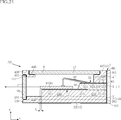
- FIG. 11 is an enlarged sectional view of an essential part showing a first modified example of the semiconductor laser device A1.
- the inner end face 36 has a shape along the z direction and is not inclined with respect to the z direction.
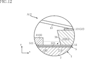
- FIG. 12 is an enlarged sectional view of an essential part showing a second modification of the semiconductor laser device A1.
- the inclination of the inward end surface 36 is different from that of the inward end surface 36 of the semiconductor laser device A1.
- the inward end surface 36 is inclined to be positioned on the other side in the x direction (rear side) as it goes from the z direction one side (upper side) to the other side in the z direction (lower side).
- the angle of the inner end face 36 can be set variously.
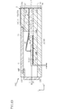
- FIG. 13 is a cross-sectional view showing a third modification of the semiconductor laser device A1.
- the semiconductor laser device A13 of this modification is different from the above-described semiconductor laser device A1 in the method of attaching the first cover 7 to the base material 1.
- the base 1 is not provided with the above-described front concave portion 171.
- the first cover 7 is attached to the front end surface 13 of the substrate 1 by adhesion, for example.
- the method and structure for attaching the first cover 7 to the substrate 1 is not particularly limited.
- FIG. 14 is a cross-sectional view showing a fourth modification of the semiconductor laser device A1.
- the configuration of the first cover 7 is different from that of the semiconductor laser device A1 described above.
- the first cover 7 has a lens portion 71.
- the lens portion 71 has a shape that bulges in the x direction, and constitutes a so-called convex lens.
- Such first cover 7 can improve the directivity in the x direction by refracting the laser light from the semiconductor laser element 6 by the lens unit 71.
- the lens part 71 which consists of convex lenses is an example, and the lens part 71 can employ
- FIG. 15 is a cross-sectional view showing a fifth modification of the semiconductor laser device A1.
- the configuration of the semiconductor laser element 6 is different from that of the semiconductor laser device A1 described above.
- the semiconductor laser device 6 has a submount 68.
- the submount 68 is made of, for example, a material such as Si, GaN, SiC, or AlN.
- the semiconductor layer 61 is formed on the upper surface of the submount 68.
- a through wire 69 is formed in the submount 68.
- the through wiring 69 is a conductive member that penetrates the submount 68 in the z direction.
- the through wiring 69 is electrically connected to an electrode (not shown) of the semiconductor layer 61.
- the first layer 2 of this modification does not have the pedestal portion 240 in the semiconductor laser device A1.
- the first main portion 210 and the bottom portion 250 have the same thickness.
- the element mounting portion 511 of the first wiring portion 51 of the wiring portion 5 is formed on the first major surface 21 of the bottom portion 250.
- the through wiring 69 of the submount 68 is electrically connected to the element mounting portion 511.
- the semiconductor laser device A15 can also be surface mounted by this modification.
- the semiconductor laser device 6 may be of a type having the submount 68 or of the type not having the submount 68.
- Various types of semiconductor laser elements 6 can be adopted by appropriately changing the configurations of the base 1 and the wiring portion 5.
- FIG. 16 is a plan view showing a sixth modification of the semiconductor laser device A1.
- FIG. 17 is a cross-sectional view taken along the line XVII-XVII in FIG.
- the one side end of the semiconductor laser element 6 in the x direction is positioned on the other side in the x direction with respect to the one side end of the pedestal portion 240 in the x direction. That is, the semiconductor laser element 6 is not configured to protrude from the pedestal portion 240, but is disposed so as to be retracted to the other side in the x direction from one side end of the pedestal portion 240 in the x direction.
- the positional relationship between the x-direction one side end of the semiconductor laser device 6 and the x-direction one side end of the pedestal portion 240 (or the x-direction one side end of the submount 68) is It is not limited. This point is the same as in the other modifications and embodiments.
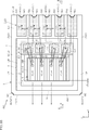
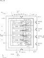
- FIG. 18 to 20 show a semiconductor laser device according to a second embodiment of the present disclosure.
- FIG. 18 is a plan view showing a semiconductor laser device A2 of the present embodiment.
- FIG. 19 is a plan view of relevant parts showing the base material 1 of the semiconductor laser device A2.
- FIG. 20 is a plan view of relevant parts showing the base material 1 of the semiconductor laser device A2.
- the arrangement of the first strip portion 512 of the first wiring portion 51 and the plurality of second strip portions 522 of the second wiring portion 52 is different from that of the semiconductor laser device A1 described above.
- the plurality of second strip portions 522 are disposed on both sides in the y direction across the first strip portion 512 in the z direction.
- two second band-shaped portions 522 are disposed on both sides in the y direction with the first band-shaped portion 512 interposed therebetween.
- the first band-shaped portion 512 is provided substantially at the center of the first main portion 210 in the x direction.
- the first connection portion 513 has a linear shape extending in the x direction, and does not have a bent shape.
- the four second connection parts 523 have bending shapes opposite to each other between the two second connection parts 523 on one side in the y direction and the two second connection parts 523 on the other side in the y direction. It has become.
- the semiconductor laser device A2 can be surface mounted. Further, according to the present embodiment, it is easy to make the path lengths of the plurality of second band-shaped portions 522 more uniform. Further, since both the first strip portion 512 and the first connecting portion 513 are linear, the inductance component of the path can be reduced.
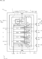
- FIG. 21 to 27 show a semiconductor laser device according to a third embodiment of the present disclosure.
- FIG. 21 is a plan view showing a semiconductor laser device A3 of the present embodiment.
- FIG. 22 is a side view showing the semiconductor laser device A3.
- FIG. 23 is a bottom view showing the semiconductor laser device A3.
- FIG. 24 is a cross-sectional view taken along the line XXIV-XXIV in FIG.
- FIG. 25 is a plan view of relevant parts showing the base material 1 of the semiconductor laser device A3.
- FIG. 26 is a plan view of relevant parts showing the base material 1 of the semiconductor laser device A3.
- FIG. 27 is a plan view of relevant parts showing the base material 1 of the semiconductor laser device A3.
- the back surface 12 of the base 1 is a mounting surface.
- the substrate 1 has a lateral groove portion 162.
- the side groove portion 162 is recessed from one side surface 15 and is along the z direction. In the present embodiment, the side groove portion 162 reaches the first back surface 22 (back surface 12). Further, in the illustrated example, the side groove portion 162 reaches the third main surface 41 (main surface 11).
- the first layer 2 has a first lateral groove 262.
- the first lateral groove portion 262 is recessed from the first side surface 25 and extends along the z direction.
- the second layer 3 has a second lateral groove 362.
- the second side groove 362 is recessed from the second side surface 35 and extends along the z direction.
- the third layer 4 has a third lateral groove 462.
- the third side groove 462 is recessed from the third side surface 45 and extends along the z direction.
- the rear groove portion 161 includes a first side groove portion 262, a second side groove portion 362, and a third side groove portion 462.
- the wiring unit 5 has a plurality of rear communication units 501 and side communication units 503.
- the plurality of rear communication portions 501 cover the plurality of rear grooves 161 as in the above-described embodiment.
- the side connection portion 503 covers the side groove portion 162 and reaches the other z-direction side end (lower side end) of the side groove portion 162. Further, in the illustrated example, the side connection portion 503 reaches the z-direction one side end (upper side end) of the side groove portion 162.
- the first wiring unit 51 includes an element mounting unit 511, a first connecting unit 513, a plurality of mounting terminal units 514, a mounting terminal unit 515, and a first connecting unit 518.
- the first connecting portion 513 extends from the element mounting portion 511 in the y direction toward the first lateral groove 262 and reaches the first lateral groove 262. Thereby, the first connecting portion 513 is in contact with the side communication portion 503.
- the mounting terminal portion 515 is formed on the first back surface 22 (back surface 12).
- the mounting terminal 515 has a rectangular shape in the z direction, and is larger than the mounting terminal 514.
- the first connecting portion 518 extends from the mounting terminal portion 515 in the y direction, and reaches the first lateral groove portion 262. Thereby, the first connecting portion 518 is in contact with the side communication portion 503.
- the element mounting portion 511 is electrically connected to the mounting terminal portion 515 via the first connection portion 513 and the side connection portions 503 and 581.
- the mounting terminal portion 515 preferably overlaps the semiconductor laser device 6 in the z direction.
- the mounting terminal 515 is, for example, a cathode electrode.
- the plurality of mounting terminal portions 514 are formed on the other side (rear side) in the x direction of the first back surface 22 (back surface 12).
- the plurality of mounting terminal portions 514 separately reach the plurality of first rear groove portions 261. Thereby, the plurality of mounting terminal portions 514 are in contact with the plurality of rear communication portions 501 separately.
- the plurality of mounting terminal portions 514 overlap the plurality of wire bonding portions 521 in the z direction.
- the mounting terminal portion 514 is, for example, an anode electrode.
- the second wiring portion 52 includes the plurality of wire bonding portions 521 and the plurality of second strip portions 522, and does not include the second connection portion 523 of the embodiment described above. Moreover, the wiring part 5 does not have the 3rd wiring part 53 of embodiment mentioned above.
- the second belt-like portion 522 is in contact with the rear communication portion 501.
- the plurality of wire bonding portions 521 are separately conducted to the plurality of mounting terminal portions 514 via the plurality of second strip portions 522 and the plurality of back connection portions 501.
- the second wiring portion 52 may have the second connection portion 523 and the wiring portion 5 may have the third wiring portion 53.
- the semiconductor laser device A3 can be surface mounted with the back surface 12 as the mounting surface. Further, according to the present embodiment, it is not necessary to form the wiring portion 5 on the main surface 11 of the base 1. Further, the mounting terminal portion 515 can be configured to overlap the semiconductor laser element 6 in the z direction. Further, the plurality of mounting terminal portions 514 can be configured to overlap the plurality of wire bonding portions 521 in the z direction. This is preferable for the miniaturization of the semiconductor laser device A3.
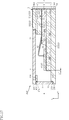
- FIG. 28 is a cross-sectional view showing a first modified example of the semiconductor laser device A3.
- the method of attaching the second cover 8 to the base 1 is different from the example described above.
- the base 1 is not provided with the above-described annular recess 440.
- the second cover 8 is attached to the major surface 11 of the substrate 1 by adhesion, for example.
- the method and structure for attaching the second cover 8 to the base 1 is not particularly limited.
- FIG. 29 to 32 show a semiconductor laser device according to a fourth embodiment of the present disclosure.
- FIG. 29 is a plan view showing a semiconductor laser device A4 of this embodiment.
- FIG. 30 is a bottom view showing A4.
- 31 is a cross-sectional view taken along the line XXXI-XXXI in FIG. 32 is a cross-sectional view taken along the line XXXII-XXXII in FIG.
- the semiconductor laser device A4 includes a thermistor 9.
- the thermistor 9 is an example of a temperature detection element for detecting the operating temperature of the semiconductor laser element 6.
- the thermistor 9 is formed on the submount 68 of the semiconductor laser device 6.
- the submount 68 includes a through wire 91 and a through wire 92 in addition to the through wire 69.
- the through wiring 91 and the through wiring 92 penetrate from the thermistor 9 to the lower surface in the drawing of the submount 68 and are made of a conductor such as metal.
- 31 and 32 schematically show the configuration in which the thermistor 9 is formed on the submount 68.
- the specific configuration of the thermistor 9 in the submount 68 can be set variously.
- the first wiring portion 51 of the wiring portion 5 includes a pair of element mounting portions 511, a pair of first connection portions 513, a plurality of mounting terminal portions 514, a mounting terminal portion 515, and a mounting terminal.
- a portion 516 and a plurality of first connecting portions 518 are provided.
- the base 1 also has a pair of lateral grooves 162.
- the pair of side groove portions 162 is formed to be divided into the pair of side surfaces 15.
- the wiring unit 5 has a pair of side communication units 503.
- the pair of side connection portions 503 covers the pair of side groove portions 162 separately.
- the plurality of element mounting portions 511 are formed on the first major surface 21 of the first layer 2. They are spaced apart in the y direction.
- the through wiring 69 and the through wiring 91 are connected to one of the element mounting portions 511.
- a through wire 92 is connected to the other element mounting portion 511.
- the pair of first connection portions 513 extends in the y direction from the pair of element mounting portions 511 toward the pair of side groove portions 162.
- the pair of first connecting portions 513 is in contact with the pair of side communication portions 503 separately.
- the plurality of mounting terminal portions 514 and the mounting terminal portions 515 have the same configuration as the mounting terminal portions 514 and the mounting terminal portions 515 of the semiconductor laser device A3 described above.
- the mounting terminal portion 515 is electrically connected to, for example, a cathode electrode (not shown) of the thermistor 9 through the first connection portion 518, the side connection portion 503, the first connection portion 513, the element mounting portion 511 and the through wiring 91. There is.
- the mounting terminal portion 516 is spaced apart from the mounting terminal portion 515 in the y direction.
- One mounting portion 516 is connected to one first connecting portion 518.
- the first connecting portion 518 is in contact with one side communication portion 503.
- the mounting terminal 516 is, for example, an anode electrode of the thermistor 9 via the first connecting portion 518, the side connecting portion 503, the first connecting portion 513, the element mounting portion 511 and the through wiring 92. (Not shown).
- the semiconductor laser device A4 can be surface mounted. Further, by providing the thermistor 9, it is possible to monitor the operating temperature of the semiconductor laser device 6 from the outside. By incorporating the thermistor 9 in the submount 68, the semiconductor laser device A4 can be miniaturized. The configuration in which the first back surface 22 (back surface 12) is a mounting surface is advantageous for downsizing of the semiconductor laser device A4.
- FIG. 33 to 35 show a semiconductor laser device according to a fifth embodiment of the present disclosure.
- FIG. 33 is a plan view showing a semiconductor laser device A5 according to the present embodiment.
- FIG. 34 is a front view showing a semiconductor laser device A5.
- FIG. 35 is a cross-sectional view taken along the line XXXV-XXXV in FIG.
- the semiconductor laser device A5 includes the thermistor 9 in the same manner as the semiconductor laser device A4.
- the thermistor 9 is configured as an element separate from the semiconductor laser element 6.
- the semiconductor laser device 6 may or may not have the submount 68. In the illustrated example, the semiconductor laser device 6 does not have the submount 68.
- the semiconductor laser device 6 is mounted on the pedestal portion 240 of the first layer 2.
- the first wiring portion 51 includes an element mounting portion 5111, a wire bonding portion 5112, and a connecting portion 5113 in addition to the element mounting portion 511 and the first connecting portion 513.
- the element mounting portion 5111 is disposed apart from the element mounting portion 511 in the y direction.
- the element mounting portion 511 and the element mounting portion 5111 are connected by a first connection portion 513.
- the element mounting portion 5111 is a portion on which the thermistor 9 is mounted.
- the wire bonding portion 5112 is disposed apart from the element mounting portion 5111 in the x direction.
- the wire 99 is connected to the wire bonding portion 5112.
- the wire 99 connects the thermistor 9 and the wire bonding portion 5112.
- the connection portion 5113 extends from the wire bonding portion 5112 toward the side groove portion 162 in the y direction.
- the connection part 5113 is in contact with the side communication part 503.
- the configuration of the back surface 12 of the semiconductor laser A5 is similar to that of the above-described semiconductor laser A4, for example. Further, as shown in FIG. 33, the thermistor 9 and the wire 99 are exposed from the opening 17 of the base 1 in the z direction. Further, as shown in FIG. 34, a part of the thermistor 9 protrudes from the emission part 18, and is arranged so as to be hidden by the front end face 13 in the x-direction view.
- the semiconductor laser device A5 can be surface mounted. Further, by providing the thermistor 9, it is possible to monitor the operating temperature of the semiconductor laser device 6 from the outside. Further, as understood from the present embodiment, the structure on which the thermistor 9 is mounted can be set variously, and the configurations of the base 1 and the wiring portion 5 may be made to correspond appropriately.
- FIG. 36 to 38 show a semiconductor laser device according to a sixth embodiment of the present disclosure.
- FIG. 36 is a plan view showing a semiconductor laser device A6 according to the present embodiment.
- FIG. 37 is a bottom view showing the semiconductor laser device A6.
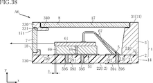
- FIG. 38 is a cross-sectional view taken along line XXXVIII-XXXVIII of FIG.
- the substrate 1 is composed of the first layer 2 and the second layer 3.
- the first layer 2 is flat and made of, for example, glass epoxy resin.
- the second layer 3 is made of, for example, an epoxy resin.
- the base 1 may be configured by a plurality of members made of different materials.
- the first layer 2 is rectangular in the z direction, and has a first major surface 21, a first back surface 22, a first front end surface 23, a first rear end surface 24, and a pair of first side surfaces 25.
- the first back surface 22 constitutes the back surface 12 and is a mounting surface in the present embodiment.
- the second layer 3 is formed, for example, by molding an epoxy resin and bonding it to the first layer 2.
- the second layer 3 has an opening 17 and an emitting portion 18, and in the illustrated example, has an annular recess 340 and a front recess 171.
- the annular recess 340 is a recess similar to the annular recess 440 in the embodiment described above, and is for providing the second cover 8.
- the wiring unit 5 includes an element mounting unit 591, a plurality of wire bonding units 592, a mounting terminal unit 593, a plurality of mounting terminal units 594, a plurality of through wirings 595, and a plurality of through wirings 596.
- the element mounting portion 591 is formed on the first major surface 21 of the first layer 2, and the semiconductor laser element 6 is mounted.
- the plurality of wire bonding portions 592 are formed on the other side (rear side) in the x direction with respect to the element mounting portion 591 and are disposed apart from each other in the y direction.
- the mounting terminal portion 593 is formed on the first back surface 22 (back surface 12), and overlaps the element mounting portion 591 in the z direction.
- the plurality of wire bonding portions 592 are formed on the first back surface 22 (the back surface 12), and overlap the plurality of wire bonding portions 592 separately in the z direction.
- the plurality of through wires 595 pass through the first layer 2 in the z direction, and are made of a conductor such as metal.
- the plurality of through wires 595 connect the element mounting portion 591 and the mounting terminal portion 593.
- the plurality of through wires 595 are arranged in a matrix.
- the plurality of through wires 596 pass through the first layer 2 in the z direction, and are made of a conductor such as metal.
- the plurality of through wires 596 individually connect the plurality of wire bonding portions 592 and the plurality of mounting terminal portions 594.
- the through wiring 596 is arranged to overlap the wire bonding portion 592 near the other side in the z direction as viewed in the z direction. Such an arrangement is suitable for providing the bonding portion of the wire 97 at a distance from the through wire 596.
- the semiconductor laser device A6 can be surface mounted. Further, by adopting the through wiring 595 and the through wiring 596, the area required for the arrangement of the wiring portion 5 can be reduced, which is preferable for the miniaturization of the semiconductor laser device A6. Further, by providing the plurality of through wires 595, the heat generated from the semiconductor laser device 6 can be transferred to the outside more efficiently.
- FIG. 39 and 40 show a semiconductor laser device according to a seventh embodiment of the present disclosure.
- FIG. 39 is a plan view showing a semiconductor laser device A7 according to this embodiment.
- FIG. 40 is a bottom view showing the semiconductor laser device A7.
- the semiconductor laser device 6 has only one waveguide 62 and an electrode 63.
- the number of wire bonding parts 592 and mounting terminal parts 594 is one.
- the semiconductor laser device A7 can be surface mounted.
- the number of waveguides 62 and electrodes 63 of the semiconductor laser device 6 in the present disclosure is not particularly limited.
- the number of waveguides 62 and the number of electrodes 63 may be one, or plural other than four. Further, for example, in the semiconductor laser device A1, when there is no need to emit laser light from the plurality of waveguides 62 at different timings, only one mounting terminal portion 531 may be provided.
- the semiconductor laser device according to the present disclosure is not limited to the embodiments described above.
- the specific configuration of each part of the semiconductor laser device according to the present disclosure can be varied in design in many ways.
- the emission unit includes a first cover that transmits light from the semiconductor laser device.
- the first cover has a lens portion that refracts light from the semiconductor laser element.
- the semiconductor laser device according to any one of appendices 2 to 4 further comprising a second cover closing the opening.
- the substrate has a mounting surface facing the thickness direction, The semiconductor laser device according to any one of appendices 2 to 5, wherein the wiring portion has a mounting terminal portion formed on the mounting surface.
- the semiconductor laser device according to appendix 11 or 12, wherein the base has an inner end face located on the other side in the first direction with respect to the semiconductor laser element and inclined with respect to the thickness direction.
- the wiring portion has at least one wire bonding portion positioned on the other side in the first direction with respect to the semiconductor laser device and positioned on the one side in the thickness direction with respect to the mounting surface.
- the semiconductor laser device according to any one of appendices 11 to 13, wherein the wire is connected to the semiconductor laser element and the wire bonding portion.
- the semiconductor laser devices are arranged in a second direction perpendicular to both the first direction and the thickness direction, and each of the semiconductor laser devices independently emits light toward one side in the first direction.
- the at least one back groove includes a plurality of back grooves arranged in the second direction
- the at least one wire bonding unit includes a plurality of wire bonding units arranged in the second direction
- the at least one back communication portion includes a plurality of back communication portions respectively formed in the plurality of back grooves.
- the wiring portion has a plurality of second strip portions, and each of the second strip portions electrically connects one of the plurality of wire bonding portions and one of the plurality of rear communication portions to each other.
Landscapes
- Physics & Mathematics (AREA)
- Condensed Matter Physics & Semiconductors (AREA)
- General Physics & Mathematics (AREA)
- Electromagnetism (AREA)
- Optics & Photonics (AREA)
- Semiconductor Lasers (AREA)
Abstract
半導体レーザ装置は、半導体レーザ素子と、前記半導体レーザ素子を支持する基材と、前記基材に形成され、前記半導体レーザ素子への導通経路を構成する配線部と、を備える。前記基材は、当該基材の厚さ方向の一方側を向き且つ前記半導体レーザ素子が搭載された搭載面と、前記厚さ方向と直角である第1方向において前記半導体レーザ素子に対して一方側に位置する出射部と、を有する。前記半導体レーザ素子からの光は、前記出射部を通じて出射される。
Description
本開示は、半導体レーザ装置に関する。
半導体レーザ装置は、各種の電子機器の光源デバイスとして広く用いられている。たとえば、特開2017-147301号公報には、従来の半導体レーザ装置の一例が開示されている。同文献に開示された半導体レーザ装置は、円板状のベース部と、ベース部の上面に設けられたヒートシンク部とを備える。ヒートシンク部には、半導体レーザ素子が搭載されている。ベース部の下面からは、2つのリードが延出している。この従来の半導体レーザ装置は、各リードを回路基板に形成された孔に挿通させた状態で、当該回路基板に実装される。
上述した形態とは異なり、電子機器の種類によっては、表面実装型の半導体レーザ装置が求められる場合がある。
本開示は、表面実装が可能な半導体レーザ装置を提供することをその一の課題とする。
本開示によって提供される半導体レーザ装置は、半導体レーザ素子と、前記半導体レーザ素子を支持する基材と、前記基材に形成され、前記半導体レーザ素子への導通経路を構成する配線部と、を備える。前記基材は、当該基材の厚さ方向の一方側を向き且つ前記半導体レーザ素子が搭載された搭載面と、前記厚さ方向と直角である第1方向において前記半導体レーザ素子に対して一方側に位置する出射部と、を有する。前記半導体レーザ素子からの光は、前記出射部を通じて出射される。
本開示の半導体レーザ装置によれば、表面実装が可能である。
本開示のその他の特徴および利点は、添付図面を参照して以下に行う詳細な説明によって、より明らかとなろう。
以下、本開示に係る実施の形態につき、図面を参照して具体的に説明する。
図1~図10は、本開示の第1実施形態に係る半導体レーザ装置A1を示している。半導体レーザ装置A1は、基材1、配線部5、半導体レーザ素子6、複数の貫通配線69、第1カバー7および第2カバー8を備えている。
以降の説明において、z方向は、基材1の厚さ方向に相当する。また、x方向は、第1方向に相当し、y方向は、第2方向に相当する。z方向において、図中の上側が「一方側」に相当し、下側が「他方側」に相当する。x方向において、一方側に相当するものとして「前側」と称し、他方側に相当するものとして、「後側」と称する場合もある。ただし、これらの「一方」「他方」「前」「後」の語句は、説明の便宜上のものであり、本開示の半導体レーザ装置の構成を限定するものではない。
本開示における「第1」、「第2」、「第3」等の用語は、単に要素を区別するためのものであり、それらの要素に順位を付することを意図していない。
基材1は、半導体レーザ素子6を支持する。少なくとも基材1の表面は、絶縁性の材料からなる。たとえば図1~図5に示すように、基材1は、主面11、裏面12、前方端面13、後方端面14、一対の側面15、開口17、出射部18、複数の後方溝部161、複数の前方溝部163および前方凹部171を有する。基材1の大きさの一例を挙げると、x方向寸法が2.0mm~7.0mm程度、y方向寸法が1.5mm~7.0mm程度、z方向寸法が0.7mm~2.5mm程度であるが、基材1の大きさや形状がこの例に限定されるわけではない。
主面11は、z方向一方側(上側)を向く面である。本実施形態においては、主面11は、実装面に相当する。図示された例においては、主面11は、z方向に対して直角である。主面11は、略矩形状である。
裏面12は、主面11の反対側にあり、z方向他方側(下側)を向く。図示された例においては、裏面12は、z方向に対して直角である。裏面12は、略矩形状である。
前方端面13は、x方向一方側(前側)を向く面であり、主面11と裏面12とを繋いでいる。図示された例においては、前方端面13は、x方向に対して直角である。
後方端面14は、x方向他方側(後側)を向く面であり、主面11と裏面12とを繋いでいる。図示された例においては、後方端面14は、x方向に対して直角である。
一対の側面15は、主面11および裏面12を繋いでおり、かつ前方端面13および後方端面14を繋いでいる。一対の側面15は、互いにy方向に離間している。図示された例においては、各側面15は、y方向に対して直角であり、略矩形状である。
開口17は、基材1によって規定された内部空間をz方向一方側(上側)に開放する部位である。図示された例においては、z方向視(平面視)において略矩形状である(図10参照)。開口17は、x方向一方側(前側)に偏って配置されている。開口17が設けられていることにより、主面11は、z方向視において矩形の環状(閉じた枠状)である。
出射部18は、半導体レーザ素子6からのレーザ光をx方向一方側(前側)に出射させるための部位である。図示された例においては、基材1によって規定された内部空間が、出射部18によりx方向一方側(前側)に開放している。出射部18は、たとえばx方向視において矩形状である(図2参照)。また、出射部18が設けられていることにより、前方端面13は、x方向視において矩形環状である。
複数の後方溝部161は、後方端面14から凹んでおり(図1参照)、それぞれがz方向に延びている(図3参照)。各後方溝部161は、主面(実装面)11に到達している。また、図示された例においては、各後方溝部161は、裏面12に到達している。後方溝部161の断面形状は、図示された例においては、半円形状であるが、本開示がこれに限定されるわけではない。複数の後方溝部161は、y方向に互いに離間して配置されている。
図1に示すように、複数の前方溝部163は、一対の側面15と前方端面13との境界部分に形成されている。各前方溝部163は、z方向に延びており、主面11および裏面12に到達している。後方溝部161の断面形状は、図示された例においては、四半円形状であるが、本開示がこれに限定されるわけではない。
図2および図5に示すように、前方凹部171は、前方端面13からx方向他方側(後側)に凹んでおり、出射部18の周囲を取り囲んでいる。前方凹部171は、x方向視において矩形環状である。前方凹部171は、第1カバー7を設けるための部分である。
図3に示すように、基材1は、複数の層を含む。図示された例では、基材1は、第1層2、第2層3および第3層4からなる。第1層2、第2層3および第3層4は、z方向に積層されている。第1層2、第2層3および第3層4は、たとえば、アルミナ、窒化アルミニウム等のセラミックスから形成されるが、本開示がこれに限定されるわけではない。なお、各層自体が、複数のセラミックス層から構成されていてもよい。図2、図3、図5および図7において、一点鎖線は、隣接するセラミックス層の境界を示している。
第1層2は、z方向において最も下側に位置している。第1層2は、第1主面21、第1裏面22、第1前方端面23、第1後方端面24、一対の第1側面25、第1主部210、一対の第1側方枠部220、第1前方枠部230、台座部240、底部250、複数の第1後方溝部261および複数の第1前方溝部263を有する。
第1主面21は、z方向上側を向く面である。本実施形態においては、第1主面21は、搭載面に相当する。図示された例においては、第1主面21は、z方向に対して直角である。
第1裏面22は、第1主面21とは反対側にあり、z方向下側を向く。図示された例においては、第1裏面22は、z方向に対して直角である。第1裏面22は、裏面12を構成している。
第1前方端面23は、x方向一方側(前側)を向く面であり、第1主面21と第1裏面22とを繋いでいる。図示された例においては、第1前方端面23は、x方向に対して直角である。第1前方端面23は、前方端面13の一部を構成している。
第1後方端面24は、x方向他方側(後側)を向く面であり、第1主面21と第1裏面22とを繋いでいる。図示された例においては、第1後方端面24は、x方向に対して直角である。第1後方端面24は、後方端面14の一部を構成している。
一対の第1側面25は、第1主面21および第1裏面22を繋いでおり、第1前方端面23および第1後方端面24を繋いでいる。一対の第1側面25は、それぞれy方向を向いている。図示された例においては、第1側面25は、y方向に対して直角である。第1側面25は、側面15の一部を構成している。
第1主部210は、第1層2のうちx方向後側に位置する部位である。図示された例においては、第1主部210は、z方向視において略矩形状である。第1主部210の厚さは、第1層2の最大厚さと同じである。
一対の第1側方枠部220は、第1主部210のy方向両側から、x方向前側に延出した部分である。第1側方枠部220の厚さは、第1層2の最大厚さと同じである。
第1前方枠部230は、一対の第1側方枠部220のx方向一方側端を繋いでおり、y方向に延びている。一対の第1側方枠部220および第1前方枠部230は、枠状の部位を構成している。第1前方枠部230には、凹部231が形成されている。凹部231は、第1前方枠部230が部分的にz方向寸法が小さくなった部位であり、前方凹部171の一部を構成する。
台座部240は、第1主部210からx方向一方側(前側)に延出しており、図示された例においては、z方向視において略矩形状である。台座部240は、一対の第1側方枠部220および第1前方枠部230から離間している。台座部240には、半導体レーザ素子6が搭載される。
底部250は、第1主面21からz方向他方側(下側)に位置する部位である。底部250は、z方向視において一対の第1側方枠部220、第1前方枠部230および台座部240に囲まれた領域に設けられている。底部250の厚さは、第1層2のz方向の最大厚さよりも小さい。
複数の第1後方溝部261は、第1後方端面24から凹んでおり、z方向に延びている。第1後方溝部261は、第1主面21および第1裏面22に到達している。第1後方溝部261の断面形状は特に限定されず、図示された例においては、半円形状である。複数の第1後方溝部261は、y方向に互いに離間して配置されている。複数の第1後方溝部261は、複数の後方溝部161の一部ずつを構成している。
複数の第1前方溝部263は、一対の第1側面25と第1前方端面23との境界部分に形成されている。第1前方溝部263は、z方向に延びており、第1主面21および第1裏面22に到達している。第1前方溝部263の断面形状は特に限定されず、図示された例においては、四半円形状である。複数の第1前方溝部263は、複数の前方溝部163の一部ずつを構成している。
第2層3は、第1層2のz方向一方側(上側)に積層されている。第2層3は、第2主面31、第2裏面32、第2前方端面33、第2後方端面34、一対の第2側面35、内方端面36、第2主部310、一対の第2側方枠部320複数の第2後方溝部361および複数の第2前方溝部363を有する。
第2主面31は、z方向一方側(上側)を向く面である。図示された例においては、第2主面31は、z方向に対して直角である。
第2裏面32は、第2主面31が向く側とは反対側である、z方向他方側(下側)を向く面であり、第1層2の第1主面21と対面している。図示された例においては、第2裏面32は、z方向に対して直角である。
第2前方端面33は、x方向一方側(前側)を向く面であり、第2主面31と第2裏面32とを繋いでいる。図示された例においては、第2前方端面33は、x方向に対して直角である。第2前方端面33は、前方端面13の一部を構成している。第2前方端面33は、y方向両側に離間した2つの領域を含む。
第2後方端面34は、x方向他方側(後側)を向く面であり、第2主面31と第2裏面32とを繋いでいる。図示された例においては、第2後方端面34は、x方向に対して直角である。第2後方端面34は、後方端面14の一部を構成している。
一対の第2側面35は、第2主面31および第2裏面32を繋いでおり、第2前方端面33および第2後方端面34を繋いでいる。一対の第2側面35は、それぞれy方向を向いている。図示された例においては、第2側面35は、y方向に対して直角である。第2側面35は、側面15の一部を構成している。
第2主部310は、第2層3のうちx方向他方側(後側)に位置する部位である。図示された例においては、第2主部310は、z方向視において略矩形状である。第2主部310の厚さは、第2層3の最大厚さと同じである。
内方端面36は、第2主部310のx方向一方側(前側)に位置する面である。内方端面36は、z方向に対して傾いており、z方向一方側(図6における図中上側)から他方側(図6における図中下側)に向かうほどz方向一方側(前側、図6における図中左側)に位置するように傾斜している。
一対の第2側方枠部320は、第2主部310のy方向両側から、x方向一方側(前側)に延出した部分である。第2側方枠部320の厚さは、第2層3の最大厚さと同じである。
一対の第2側方枠部320には、それぞれ凹部321が形成されている。凹部321は、第2側方枠部320のうち第2前方端面33からx方向他方側(後側)に凹む部位である。また、凹部321は、y方向内側に位置している。一対の凹部321は、前方凹部171の一部を構成する。
複数の第2後方溝部361は、第2後方端面34から凹んでおり、z方向に延びている。第2後方溝部361は第2主面31および第2裏面32に到達している。第2後方溝部361の断面形状は特に限定されず、図示された例においては、半円形状である。複数の第2後方溝部361は、y方向に互いに離間して配置されている。複数の第2後方溝部361は、複数の後方溝部161の一部ずつを構成している。
複数の第2前方溝部363は、一対の第2側面35と第2前方端面33との境界部分に形成されている。第2前方溝部363は、z方向に延びており、第2主面31および第2裏面32に到達している。第2前方溝部363の断面形状は特に限定されず、図示された例においては、四半円形状である。複数の第2前方溝部363は、複数の前方溝部163の一部ずつを構成している。
第3層4は、z方向において最も一方側(上側)に位置している。第3層4は、第2層3のz方向一方側(上側)に積層されている。第3層4は、第3主面41、第3裏面42、第3前方端面43、第3後方端面44、一対の第3側面45、第3主部410、一対の第3側方枠部420、第3前方枠部430、複数の第3後方溝部461および複数の第3前方溝部463を有する。
第3主面41は、z方向一方側(上側)を向く面である。図示された例においては、第3主面41は、z方向に対して直角である。本実施形態においては、第3主面41は、主面11を構成している。
第3裏面42は、第3主面41が向く側とは反対側である、z方向他方側(下側)を向く面であり、第2層3の第2主面31と対面している。図示された例においては、第3裏面42は、z方向に対して直角である。
第3前方端面43は、x方向一方側(前側)を向く面であり、第3主面41と第3裏面42とを繋いでいる。図示された例においては、第3前方端面43は、x方向に対して直角である。第3前方端面43は、前方端面13の一部を構成している。
第3後方端面44は、x方向他方側(後側)を向く面であり、第3主面41と第3裏面42とを繋いでいる。図示された例においては、第3後方端面44は、x方向に対して直角である。第3後方端面44は、後方端面14の一部を構成している。
一対の第3側面45は、第3主面41および第3裏面42を繋いでおり、第3前方端面43および第3後方端面44を繋いでいる。一対の第3側面45は、それぞれy方向を向いている。図示された例においては、第3側面45は、y方向に対して直角である。第3側面45は、側面15の一部を構成している。
第3主部410は、第3層4のうちx方向他方側(後側)に位置する部位である。図示された例においては、第3主部410は、z方向視において略矩形状である。第3主部410の厚さは、第2層3の最大厚さと同じである。
一対の第3側方枠部420は、第3主部410のy方向両側から、x方向一方側(前側)に延出した部分である。
第3前方枠部430は、一対の第3側方枠部420のx方向一方側端を繋いでおり、y方向に延びている。一対の第3側方枠部420および第3前方枠部430は、枠状の部位を構成している。図5に示すように、第3前方枠部430には、凹部431が形成されている。凹部431は、第3前方端面43からx方向他方側(後側)に凹んだ部位であり、前方凹部171の一部を構成する。
複数の第3後方溝部461は、第3後方端面44から凹んでおり、z方向に延びている。第3後方溝部461は、第3主面41および第3裏面42に到達している。第3後方溝部461の断面形状は特に限定されず、図示された例においては、半円形状である。複数の第3後方溝部461は、y方向に互いに離間して配置されている。複数の第3後方溝部461は、複数の後方溝部161の一部ずつを構成している。
複数の第3前方溝部463は、一対の第3側面45と第3前方端面43との境界部分に形成されている。第3前方溝部463は、z方向に延びており、第3主面41および第3裏面42に到達している。第3前方溝部463の断面形状は特に限定されず、図示された例においては、四半円形状である。複数の第3前方溝部463は、複数の前方溝部163の一部ずつを構成している。
本実施形態においては、第3層4に、開口17が形成されている。また、第3層4には、環状凹部440が形成されている。環状凹部440は、第3層4のうち開口17を取り囲む部分が、第3主面41(主面11)からz方向他方側(下側)に凹んだ部分である。環状凹部440は、z方向視において、矩形環状である。環状凹部440は、第2カバー8を設けるための部位である。
配線部5は、基材1に形成されており、半導体レーザ素子6への導通経路を構成するものである。図1~図3および図5~図10に示すように、本実施形態においては、配線部5は、第1配線部51、第2配線部52、第3配線部53、複数の後方連絡部501および複数の前方部505を有する。配線部5は、適切な導電性を有する材質からなり、たとえばめっきや貼り付け等によって形成される。配線部5の材質としては、たとえば、Cu、Ni、Ti、Au等が適宜選択される。また、配線部5のうち、はんだを付着させる部位には、Snからなる表層を設けておいてもよい。
第1配線部51は、基材1の第1層2に形成された部分である。本実施形態においては、第1配線部51は、素子搭載部511、第1帯状部512および第1連結部513を有する。
素子搭載部511は、基材1の第1層2の台座部240の第1主面21に形成されている。素子搭載部511は、半導体レーザ素子6が搭載される部分である。図示された例においては、素子搭載部511は、z方向視において略矩形状であり、台座部240の大部分を覆っている。
第1帯状部512は、第1層2の第1主部210に形成されており、複数の第1後方溝部261のうちy方向において図8における最も図中下側に位置するものに到達している。また、第1帯状部512は、この第1後方溝部261からx方向に沿って延びている。
第1連結部513は、素子搭載部511と第1帯状部512とを連結している。第1連結部513の形状や大きさは特に限定されず、図示された例においては、2つの屈曲部分を有する形状である。
第2配線部52は、基材1の第2層3に形成された部分である。第2配線部52は、複数のワイヤボンディング部521、複数の第2帯状部522および複数の第2連結部523を有する。
複数のワイヤボンディング部521は、複数のワイヤ67が接続される部位である。本実施形態においては、複数のワイヤボンディング部521は、y方向に配列されており、第2主部310のx方向一方側(前側)部分に形成されている。ワイヤボンディング部521の形状は特に限定されず、図示された例においては、矩形状である。図1に示すように、複数のワイヤボンディング部521は、z方向視において第3層4から露出している。
複数の第2帯状部522は、第2層3の第2主部310に形成されており、複数の第2後方溝部361のうちy方向において図9における図中上側の4つの第2後方溝部361に到達している。第2帯状部522は、第2後方溝部361からx方向に沿って延びている。なお、図8に示すように、第1帯状部512と複数の第2帯状部522とは、z方向視において互いにy方向に離間して配列されている。
複数の第2連結部523は、複数のワイヤボンディング部521と複数の第2帯状部522とを連結している。第2連結部523の形状や大きさは特に限定されず、図示された例においては、2つの屈曲部分を有する形状である。
第3配線部53は、基材1の第3層4に形成された部分である。第3配線部53は、複数の実装端子部531および実装端子部532を有する。
複数の実装端子部531は、第3層4の第3主部410に形成されており、y方向に互いに離間して配列されている。複数の実装端子部531は、複数の第3後方溝部461のうちy方向において図10における図中上側の4つの第3後方溝部461に到達している。実装端子部531は、第3後方溝部461からx方向に沿って延びている。実装端子部531のy方向寸法は、第2帯状部522のy方向寸法よりも大きい。複数の実装端子部531は、たとえばアノード電極である。
実装端子部532は、第3層4の第3主部410に形成されている。実装端子部532は、複数の第3後方溝部461のうちy方向において図10における最も図中下側に位置するものに到達している。また、実装端子部532は、この第3後方溝部461からx方向に沿って延びている。実装端子部532のy方向寸法は、第1帯状部512のy方向寸法よりも大きい。複数の実装端子部531および実装端子部532は、y方向に互いに離間配列されている。実装端子部532は、たとえばカソード電極である。
図1に示すように、本実施形態においては、z方向視において、互いに導通するワイヤボンディング部521の中心O1と実装端子部531の中心O2とは、y方向において距離Gだけずれて配置されている。なお、図1に示された複数の距離Gは、互いに同じ寸法でもよいし、互いに異なる寸法であってもよい。また、ワイヤボンディング部521のy方向端縁を仮想的に延長した延長線Eは、実装端子部531と交差している。
図3に示すように、複数の後方連絡部501は、基材1の複数の後方溝部161のうち図中右側の4つの後方溝部161を覆うように形成されている。本実施形態においては、後方連絡部501は、後方溝部161のz方向一方側端(上側端)に到達している。また、図示された例においては、後方連絡部501は、後方溝部161のz方向他方側端(下側端)に到達している。後方連絡部501は、それぞれ第2配線部52の第2帯状部522および第3配線部53の実装端子部531と接しており、これらと導通している。これにより、ワイヤボンディング部521は、第2連結部523、第2帯状部522および後方連絡部501を介して実装端子部531に導通している。
後方連絡部502は、基材1の複数の後方溝部161のうち図3における図中左端の後方溝部161を覆うように形成されている。本実施形態においては、後方連絡部502は、後方溝部161のz方向一方側端(上側端)に到達している。また、図示された例においては、後方連絡部502は、後方溝部161のz方向他方側端(下側端)に到達している。後方連絡部502は、第1配線部51の第1帯状部512および第3配線部53の実装端子部532と接しており、これらと導通している。これにより、素子搭載部511は、第1連結部513、第1帯状部512および後方連絡部502を介して実装端子部532に導通している。
図2に示すように、複数の前方部505は、複数の前方溝部163をそれぞれ覆っている。図示された例においては、前方部505は、前方溝部163の全体を覆っており、前方溝部163のz方向両端に到達している。前方部505は、第1配線部51、第2配線部52および第3配線部53とは接しておらず、これらの各部とは導通していない。
半導体レーザ素子6は、所定の波長のレーザ光を出射する素子である。半導体レーザ素子6の具体的構成は特に限定されず、本実施形態においては、半導体レーザ素子6は、半導体層61、複数の導波路62および複数の電極63を有する。
半導体層61は、半導体材料からなる複数の層が積層されたものであり、たとえば活性層とこれを挟むn型クラッド層およびp型クラッド層を含む。活性層内において電子と正孔とが再結合することにより、光が発せられる。
複数の導波路62は、活性層において発せられた光をx方向において繰り返し反射させることにより、所定波長のレーザ光を生成する部位である。本実施形態においては、複数の導波路62は、y方向に互いに離間して配列されており、各々がx方向に沿って延びている。半導体レーザ素子6は、マルチビームタイプであり、各導波路62から個別に(すなわち、他の導波路とは独立に)レーザ光を出射可能である。
複数の電極63は、複数の導波路62に対応して設けられており、y方向に互いに離間して配列されている。複数の電極63には、複数のワイヤ67が各別に接続されている。なお、図示された例においては、より大きな電流を流すことを目的として、1つの電極63に複数のワイヤ67が接続されている。
本実施形態においては、半導体レーザ素子6の半導体層61の下面に設けられた電極(図示略)が、Agペースト等の導電性接合材(図示略)によって素子搭載部511に導通接合されている。これにより、半導体レーザ素子6は、台座部240の第1主面21に搭載されている。なお、図示された例においては、図1および図5に示すように、半導体レーザ素子6のx方向一方側端は、台座部240からx方向一方側に長さLだけ突出している。この突出は、半導体レーザ素子6からの光が台座部240に干渉することを抑制するのに好ましく、以降の図においても、同様の構成として示されている。ただし、半導体レーザ素子6からの光の干渉が許容される場合等は、半導体レーザ素子6のx方向一方側端と台座部240のx方向一方側端とが、z方向視において略一致するなど、半導体レーザ素子6が台座部240から突出しない構成であってもよい。
半導体レーザ素子6が備える導波路62の個数は、特に限定されない。図示された例においては、半導体レーザ素子6は、4つの導波路62を有している。これに対応して、半導体レーザ素子6は、4つの電極63を有する。また、第2配線部52は、4つのワイヤボンディング部521、4つの第2帯状部522および4つの第2連結部523を有する。基材1は、5つの後方溝部161を有しており、配線部5は、4つの後方連絡部501と1つの後方連絡部502とを有する。また、第3配線部53は、4つの実装端子部531と1つの実装端子部532とを有する。
第1カバー7は、出射部18を塞いでおり、半導体レーザ素子6からの光を透過させる材質からなる。本実施形態においては、第1カバー7は、たとえば透明なガラスからなる。また、第1カバー7は、出射効率を改善するための所定のコーティングが施されていてもよい。図示された例においては、第1カバー7は、x方向視において矩形状であり、基材1の前方凹部171に収容されている。第1カバー7の基材1への取付け手法は特に限定されず、たとえば紫外線硬化樹脂等の接着材によって接合される。また、図示された例においては、第1カバー7は、x方向寸法が一様である平板状である。
第2カバー8は、開口17を塞いでいる。第2カバー8の材質は特に限定されず、本実施形態においては、たとえばガラスからなる。また、第2カバー8は、所定の外来光線を減衰させるための所定のコーティングが施されていてもよい。図示された例においては、第2カバー8は、z方向視において矩形状であり、基材1の環状凹部440に収容されている。第2カバー8の基材1への取付け手法は特に限定されず、たとえば紫外線硬化樹脂等の接着材によって接合される。また、図示された例においては、第2カバー8は、z方向寸法が一様である平板状である。
なお、第1カバー7および第2カバー8を備える構成においては、第1カバー7および第2カバー8によって、基材1によって規定された内部空間を密閉する構造であってもよい。この場合、第1カバー7および第2カバー8の基材1への取り付けを減圧環境において行うことにより、半導体レーザ装置A1の完成後において、第1カバー7および第2カバー8が大気圧によって基材1に押し付けられる構成であることが好ましい。
次に、半導体レーザ装置A1の作用について説明する。
本実施形態によれば、主面11(第3主面41)に複数の実装端子部531および実装端子部532が形成されており、主面11(第3主面41)が実装面とされている。このため、半導体レーザ装置A1を回路基板(図示略)等に表面実装することができる。
主面11を実装面とした場合、半導体レーザ装置A1からは、x方向一方側(前側)へとレーザ光を出射することが可能である。これにより、リードを用いて実装するタイプの半導体レーザ装置に対し、レーザ光の出射方向を90°異ならせることができる。
開口17は、実装面としての主面11から開口する構成である。これにより、半導体レーザ装置A1の製造工程において、基材1を形成した後に、たとえば開口17が鉛直方向上側を向く姿勢とする。次いで、この状態で、半導体レーザ素子6の搭載、ワイヤ67のボンディング、第1カバー7および第2カバー8の取り付けを行う。そして、鉛直方向上側を向く状態である複数の実装端子部531および実装端子部532を用いて、半導体レーザ素子6の導通試験や発光試験を行うことが可能である。このため、複数の実装端子部531および実装端子部532を用いた試験を行うために、半導体レーザ装置A1の完成後に半導体レーザ装置A1を反転させる等の作業が不要となる。また、基材1が、出射部18において中空となっていることにより、半導体レーザ装置A1の作動に伴って生じる応力を緩和することができる。
台座部240および底部250を設けることにより、台座部240のx方向一方側の第1主面21は、底部250からz方向一方側に位置する構成となる。この第1主面21を搭載面として用いることにより、半導体レーザ素子6から出射されたレーザ光が、台座部240および底部250によって遮られることを抑制することが可能である。また、半導体レーザ素子6のx方向一方側端(前側端)を台座部240からx方向一方側(前側)に突出させる構成は、レーザ光が遮られることを抑制するのに好ましい。ただし、半導体レーザ素子6は、台座部240から突出する構成には限定されない。
複数の第2帯状部522は、半導体レーザ素子6に対してx方向他方側(後側)に延びている。すなわち、複数の第2帯状部522は、半導体レーザ素子6のレーザ光が出射される側とは反対側に設けられている。これにより、複数の第2帯状部522を直線状とし、互いの距離が大きく異ならない配置とすることが可能である。これは、半導体レーザ素子6の複数の導波路62および複数の電極63への導通経路の経路長を均一化するのに適している。また、第1帯状部512が、複数の第2帯状部522と同様に直線状であり、且つz方向視において複数の第2帯状部522とy方向に離間して配列されていることにより、通電時の意図しない相互干渉を抑制することができる。これは、複数の半導体レーザ素子6を所望のタイミングで個別に発光させるのに好ましい。
基材1には、内方端面36が形成されている。半導体レーザ素子6からは、x方向一方側(前側)だけでなく、x方向他方側(後側)にも光が出射される場合がある。好ましくは、後方に出射された光は、前方へ出射された光と重畳しない方がよい。本実施形態では、半導体レーザ素子6のx方向他方側(後側)に内方端面36が設けられている。これにより、半導体レーザ素子6から後側に進行したレーザ光が出射部18へと向かうことを抑制することができる。
実装面としての主面11において、複数の実装端子部531および実装端子部532は、x方向他方側(後方側)に偏って配置されている。一方、複数の前方部505は、複数の実装端子部531および実装端子部532とは離間しており、x方向一方側(前方側)に配置されている。これにより、半導体レーザ装置A1を回路基板等に実装した際に、溶融はんだの表面張力を半導体レーザ装置A1に、よりバランス良く作用させることが可能である。したがって、半導体レーザ装置A1の実装位置や姿勢をより適切に設定することができる。
図11~図40は、本開示の変形例および他の実施形態を示している。なお、これらの図において、上記実施形態と同一または類似の要素には、上記実施形態と同一の符号を付している。なお、上述した実施形態と、以下に説明する変形例および実施形態とは、互いの部分的な構成を適宜採用可能であることはもちろんであり、様々な組み合わせが実現される。
図11は、半導体レーザ装置A1の第1変形例を示す要部拡大断面図である。本変形例の半導体レーザ装置A11においては、内方端面36は、z方向に沿った形状であり、z方向に対して傾斜していない。
図12は、半導体レーザ装置A1の第2変形例を示す要部拡大断面図である。本変形例の半導体レーザ装置A12においては、内方端面36の傾きが、半導体レーザ装置A1の内方端面36とは、異なっている。本変形例においては、内方端面36は、z方向一方側(上側)からz方向他方側(下側)に向かうほど、x方向他方側(後側)に位置するように傾いている。
これらの変形例から理解されるように、内方端面36の角度は、種々に設定可能である。
図13は、半導体レーザ装置A1の第3変形例を示す断面図である。本変形例の半導体レーザ装置A13においては、第1カバー7の基材1への取付け手法が上述した半導体レーザ装置A1と異なっている。
本変形例においては、基材1には、上述の前方凹部171が設けられていない。第1カバー7は、基材1の前方端面13にたとえば接着によって取り付けられている。本変形例から理解されるように、第1カバー7の基材1への取付け手法や取付け構造は特に限定されない。
図14は、半導体レーザ装置A1の第4変形例を示す断面図である。本変形例の半導体レーザ装置A14においては、第1カバー7の構成が上述した半導体レーザ装置A1と異なっている。
本変形例においては、第1カバー7は、レンズ部71を有する。レンズ部71は、x方向に膨出する形状であり、いわゆる凸レンズを構成している。このような第1カバー7は、レンズ部71によって半導体レーザ素子6からのレーザ光を屈折させることにより、x方向における指向性をより高めることができる。なお、凸レンズからなるレンズ部71は一例であり、レンズ部71は、凹レンズ等の様々な形状のレンズを適宜採用可能である。
図15は、半導体レーザ装置A1の第5変形例を示す断面図である。本変形例の半導体レーザ装置A15においては、半導体レーザ素子6の構成が上述した半導体レーザ装置A1と異なっている。
本変形例においては、半導体レーザ素子6は、サブマウント68を有する。サブマウント68は、たとえばSi、GaN、SiC、AlN等の材料からなる。サブマウント68は、その上面に半導体層61が形成されている。
サブマウント68には、貫通配線69が形成されている。貫通配線69は、サブマウント68をz方向に貫通する導通部材である。貫通配線69は、半導体層61の電極(図示略)に導通している。
本変形例の第1層2は、半導体レーザ装置A1における台座部240を有していない。また、第1主部210と底部250とは、互いの厚さが同じである。配線部5の第1配線部51の素子搭載部511は、底部250の第1主面21に形成されている。サブマウント68の貫通配線69は、素子搭載部511に導通している。
本変形例によっても、半導体レーザ装置A15を表面実装することができる。また、半導体レーザ素子6は、サブマウント68を有するタイプのものでも、サブマウント68を有さないタイプのものであってもよい。基材1および配線部5の構成を適宜変更する事により、様々なタイプの半導体レーザ素子6を採用可能である。
図16は、半導体レーザ装置A1の第6変形例を示す平面図である。図17は、図16のXVII-XVII線に沿う断面図である。
本変形例の半導体レーザ装置A16においては、半導体レーザ素子6のx方向一方側端が、台座部240のx方向一方側端に対して長さL’だけx方向他方側に位置している。すなわち、半導体レーザ素子6は、台座部240から突出した構成ではなく、台座部240のx方向一方側端からx方向他方側に退避した配置とされている。
このような変形例によれば、半導体レーザ素子6と素子搭載部511(台座部240)とが重なり合う面積を増大させることが可能である。これにより、半導体レーザ素子6の発光に伴う熱を台座部240(基材1)へとより効率よく伝達することができる。また、半導体レーザ素子6と素子搭載部511(台座部240)との接合面積が増大することにより、互いの接合強度を高めることができる。また、本変形例から理解されるように、半導体レーザ素子6のx方向一方側端と台座部240のx方向一方側端(あるいはサブマウント68のx方向一方側端)との位置関係は何ら限定されない。この点は、他の変形例および実施形態においても同様である。
図18~図20は、本開示の第2実施形態に係る半導体レーザ装置を示している。図18は、本実施形態の半導体レーザ装置A2を示す平面図である。図19は、半導体レーザ装置A2の基材1を示す要部平面図である。図20は、半導体レーザ装置A2の基材1を示す要部平面図である。
半導体レーザ装置A2においては、第1配線部51の第1帯状部512と第2配線部52の複数の第2帯状部522との配置が、上述した半導体レーザ装置A1と異なっている。
本実施形態においては、複数の第2帯状部522は、z方向視において第1帯状部512を挟んでy方向両側に配置されている。図示された例においては、2つずつの第2帯状部522が第1帯状部512を挟んでy方向両側に配置されている。
図19に示すように、第1帯状部512は、第1主部210のx方向略中央に設けられている。また、第1連結部513は、x方向に延びる直線状であり、屈曲形状ではない。
図20に示すように、4つの第2連結部523は、y方向一方側の2つの第2連結部523とy方向他方側の2つの第2連結部523とで、屈曲形状が互いに反対向きとなっている。
このような実施形態によっても、半導体レーザ装置A2を表面実装することができる。また、本実施形態によれば、複数の第2帯状部522の経路長をより均一にしやすい。また、第1帯状部512および第1連結部513がともに直線状であることにより、当該経路のインダクタンス成分を縮小させることができる。
図21~図27は、本開示の第3実施形態に係る半導体レーザ装置を示している。図21は、本実施形態の半導体レーザ装置A3を示す平面図である。図22は、半導体レーザ装置A3を示す側面図である。図23は、半導体レーザ装置A3を示す底面図である。図24は、図21のXXIV-XXIV線に沿う断面図である。図25は、半導体レーザ装置A3の基材1を示す要部平面図である。図26は、半導体レーザ装置A3の基材1を示す要部平面図である。図27は、半導体レーザ装置A3の基材1を示す要部平面図である。
半導体レーザ装置A3においては、図23および図24に示すように、基材1の裏面12が実装面とされている。
基材1は、側方溝部162を有する。側方溝部162は、一方の側面15から凹んでおり、z方向に沿っている。本実施形態においては、側方溝部162は、第1裏面22(裏面12)に到達している。また、図示された例においては、側方溝部162は、第3主面41(主面11)に到達している。
第1層2は、第1側方溝部262を有する。第1側方溝部262は、第1側面25から凹んでおり、z方向に沿っている。第2層3は、第2側方溝部362を有する。第2側方溝部362は、第2側面35から凹んでおり、z方向に沿っている。第3層4は、第3側方溝部462を有する。第3側方溝部462は、第3側面45から凹んでおり、z方向に沿っている。後方溝部161は、第1側方溝部262、第2側方溝部362および第3側方溝部462からなる。
配線部5は、複数の後方連絡部501および側方連絡部503を有する。複数の後方連絡部501は、上述した実施形態と同様に、複数の後方溝部161を覆っている。側方連絡部503は、側方溝部162を覆っており、側方溝部162のz方向他方側端(下側端)に到達している。また、図示された例においては、側方連絡部503は、側方溝部162のz方向一方側端(上側端)に到達している。
図23および図25に示すように、第1配線部51は、素子搭載部511、第1連結部513、複数の実装端子部514、実装端子部515および第1連結部518を有する。第1連結部513は、素子搭載部511から第1側方溝部262に向かってy方向に延びており、第1側方溝部262に到達している。これにより、第1連結部513は、側方連絡部503に接している。
実装端子部515は、第1裏面22(裏面12)に形成されている。実装端子部515は、z方向視矩形状であり、実装端子部514より大きい。第1連結部518は、実装端子部515からy方向に延びており、第1側方溝部262に到達している。これにより、第1連結部518は、側方連絡部503に接している。この結果、素子搭載部511は、第1連結部513、側方連絡部503および581を介して、実装端子部515と導通している。なお、図24および図25に示すように、実装端子部515は、z方向視において半導体レーザ素子6と重なる構成とすることが好ましい。実装端子部515は、たとえばカソード電極である。
複数の実装端子部514は、第1裏面22(裏面12)のx方向他方側(後側)寄りに形成されている。複数の実装端子部514は、複数の第1後方溝部261に各別に到達している。これにより、複数の実装端子部514は、複数の後方連絡部501と各別に接している。なお、図24および図26に示すように、複数の実装端子部514は、複数のワイヤボンディング部521とz方向視において重なる構成とすることが好ましい。実装端子部514は、たとえばアノード電極である。
図示された例においては、第2配線部52は、複数のワイヤボンディング部521および複数の第2帯状部522を有しており、上述した実施形態の第2連結部523を有していない。また、配線部5は、上述した実施形態の第3配線部53を有さない。第2帯状部522は、後方連絡部501に接している。この結果、複数のワイヤボンディング部521は、複数の第2帯状部522および複数の後方連絡部501を介して、複数の実装端子部514に各別に導通している。ただし、第2配線部52が第2連結部523を有し、配線部5が第3配線部53を有する構成であってもよい。
このような実施形態によっても、裏面12を実装面として、半導体レーザ装置A3を表面実装することができる。また、本実施形態によれば、基材1の主面11には、配線部5を形成する必要がない。また、実装端子部515を半導体レーザ素子6とz方向視において重なる構成とすることができる。また、複数の実装端子部514を複数のワイヤボンディング部521とz方向視において重なる構成とすることができる。これは、半導体レーザ装置A3の小型化に好ましい。
図28は、半導体レーザ装置A3の第1変形例を示す断面図である。本変形例の半導体レーザ装置A31においては、第2カバー8の基材1への取付け手法が上述した例と異なっている。
本変形例においては、基材1には、上述の環状凹部440が設けられていない。第2カバー8は、基材1の主面11にたとえば接着によって取り付けられている。本変形例から理解されるように、第2カバー8の基材1への取付け手法や取付け構造は特に限定されない。
図29~図32は、本開示の第4実施形態に係る半導体レーザ装置を示している。図29は、本実施形態の半導体レーザ装置A4を示す平面図である。図30は、A4を示す底面図である。図31は、図29のXXXI-XXXI線に沿う断面図である。図32は、図29のXXXII-XXXII線に沿う断面図である。
本実施形態においては、半導体レーザ装置A4は、サーミスタ9を備える。サーミスタ9は、半導体レーザ素子6の動作温度を検出するための温度検出素子の一例である。
図示された例においては、サーミスタ9は、半導体レーザ素子6のサブマウント68に形成されている。図32に示すように、サブマウント68は、貫通配線69に加えて、貫通配線91および貫通配線92を有する。貫通配線91および貫通配線92は、サーミスタ9からサブマウント68の図中下面までを貫通しており、金属等の導電体からなる。なお、図31および図32は、サブマウント68にサーミスタ9が形成された構成を模式的に示したものである。サブマウント68におけるサーミスタ9の具体的構成は、種々に設定可能である。
図30~図32に示すように、配線部5の第1配線部51は、一対の素子搭載部511、一対の第1連結部513、複数の実装端子部514、実装端子部515、実装端子部516および複数の第1連結部518を有する。また、基材1は、一対の側方溝部162を有する。一対の側方溝部162は、一対の側面15に分かれて形成されている。配線部5は、一対の側方連絡部503を有する。一対の側方連絡部503は、一対の側方溝部162を各別に覆っている。
複数の素子搭載部511は、第1層2の第1主面21に形成されており。y方向に離間して配置されている。一方の素子搭載部511には、貫通配線69と貫通配線91とが繋がっている。他方の素子搭載部511には、貫通配線92が繋がっている。
一対の第1連結部513は、一対の素子搭載部511から一対の側方溝部162に向けてy方向に延びている。一対の第1連結部513は、一対の側方連絡部503に各別に接している。
複数の実装端子部514および実装端子部515は、上述した半導体レーザ装置A3の実装端子部514および実装端子部515と同様の構成である。実装端子部515は、第1連結部518、側方連絡部503、第1連結部513、素子搭載部511および貫通配線91を介して、サーミスタ9のたとえばカソード電極(図示略)に導通している。
実装端子部516は、実装端子部515に対してy方向に離間して配置されている。実装端子部516には、一方の第1連結部518が繋がっている。第1連結部518は、一方の側方連絡部503に接している。図32に示すように、実装端子部516は、第1連結部518、側方連絡部503、第1連結部513、素子搭載部511および貫通配線92を介して、サーミスタ9のたとえばアノード電極(図示略)に導通している。
このような実施形態によっても、半導体レーザ装置A4を表面実装することができる。また、サーミスタ9を備えることにより、半導体レーザ素子6の動作温度を外部から監視することが可能である。サーミスタ9をサブマウント68に内蔵することにより、半導体レーザ装置A4の小型化を図ることができる。第1裏面22(裏面12)を実装面とする構成は、半導体レーザ装置A4の小型化に有利である。
図33~図35は、本開示の第5実施形態に係る半導体レーザ装置を示している。図33は、本実施形態に係る半導体レーザ装置A5を示す平面図である。図34は、半導体レーザ装置A5を示す正面図である。図35は、図33のXXXV-XXXV線に沿う断面図である。
半導体レーザ装置A5は、半導体レーザ装置A4と同様にサーミスタ9を備える。本実施形態においては、サーミスタ9は、半導体レーザ素子6とは別体の素子として構成されている。なお、半導体レーザ素子6は、サブマウント68を有していても有していなくてもよい。図示された例においては、半導体レーザ素子6は、サブマウント68を有していない。半導体レーザ素子6は、第1層2の台座部240に搭載されている。
第1配線部51は、素子搭載部511および第1連結部513に加えて、素子搭載部5111、ワイヤボンディング部5112および連結部5113を有する。素子搭載部5111は、素子搭載部511に対してy方向に離間して配置されている。素子搭載部511と素子搭載部5111とは、第1連結部513によって連結されている。素子搭載部5111は、サーミスタ9が搭載される部位である。ワイヤボンディング部5112は、素子搭載部5111に対してx方向に離間して配置されている。ワイヤボンディング部5112には、ワイヤ99が接続される。ワイヤ99は、サーミスタ9とワイヤボンディング部5112とを接続している。連結部5113は、ワイヤボンディング部5112から側方溝部162に向かってy方向に延びている。連結部5113は、側方連絡部503に接している。
半導体レーザ装置A5の裏面12における構成は、たとえば上述した半導体レーザ装置A4と同様である。また、図33に示すように、サーミスタ9およびワイヤ99は、z方向視において基材1の開口17から露出している。また、図34に示すように、サーミスタ9は、その一部が出射部18からはみ出しており、x方向視において前方端面13に隠れた配置となっている。
このような実施形態によっても、半導体レーザ装置A5を表面実装することができる。また、サーミスタ9を備えることにより、半導体レーザ素子6の動作温度を外部から監視することが可能である。また、本実施形態から理解されるように、サーミスタ9を搭載する構造は、様々に設定可能であり、基材1および配線部5の構成を適宜対応させればよい。
図36~図38は、本開示の第6実施形態に係る半導体レーザ装置を示している。図36は、本実施形態に係る半導体レーザ装置A6を示す平面図である。図37は、半導体レーザ装置A6を示す底面図である。図38は、図36のXXXVIII-XXXVIII線に沿う断面図である。
本実施形態においては、基材1は、第1層2および第2層3からなる。第1層2は、たとえばガラスエポキシ樹脂からなる、平板状である。第2層3は、たとえばエポキシ樹脂からなる。このように、基材1は、互いに異なる材質からなる複数の部材によって構成されていてもよい。
第1層2は、z方向視において矩形状であり、第1主面21、第1裏面22、第1前方端面23、第1後方端面24および一対の第1側面25を有する。第1裏面22は、裏面12を構成しており、本実施形態における実装面である。
第2層3は、たとえば、エポキシ樹脂を金型成形したものを第1層2に接合したものである。第2層3は、開口17および出射部18を有しており、図示された例においては、環状凹部340および前方凹部171を有する。環状凹部340は、上述した実施形態における環状凹部440と同様の凹部であり、第2カバー8を設けるためのものである。
配線部5は、素子搭載部591、複数のワイヤボンディング部592、実装端子部593、複数の実装端子部594、複数の貫通配線595および複数の貫通配線596を有する。
素子搭載部591は、第1層2の第1主面21に形成されており、半導体レーザ素子6が搭載されている。複数のワイヤボンディング部592は、素子搭載部591に対してx方向他方側(後側)に形成されており、y方向に互いに離間して配置されている。
実装端子部593は、第1裏面22(裏面12)に形成されており、z方向視において素子搭載部591と重なる。複数のワイヤボンディング部592は、第1裏面22(裏面12)に形成されており、複数のワイヤボンディング部592とz方向視において各別に重なる。
複数の貫通配線595は、第1層2をz方向に貫通しており、金属等の導電体からなる。複数の貫通配線595は、素子搭載部591と実装端子部593とを繋いでいる。図示された例においては、複数の貫通配線595は、マトリクス状に配置されている。
複数の貫通配線596は、第1層2をz方向に貫通しており、金属等の導電体からなる。複数の貫通配線596は、複数のワイヤボンディング部592と複数の実装端子部594とを各別に繋いでいる。図36に示すように、貫通配線596は、z方向視においてワイヤボンディング部592のx方向他方側寄り部分に重なるように配置されている。このような配置は、ワイヤ97のボンディング部分を、貫通配線596から離れた位置に設けるのに適している。
このような実施形態によっても、半導体レーザ装置A6を表面実装することができる。また、貫通配線595および貫通配線596を採用することにより、配線部5の配置に要する面積を縮小することが可能であり、半導体レーザ装置A6の小型化に好ましい。また、複数の貫通配線595を備えることにより、半導体レーザ素子6から発した熱をより効率よく外部に伝達することができる。
図39および図40は、本開示の第7実施形態に係る半導体レーザ装置を示している。図39は、本実施形態に係る半導体レーザ装置A7を示す平面図である。図40は、半導体レーザ装置A7を示す底面図である。
本実施形態においては、半導体レーザ素子6が、1つのみの導波路62および電極63を有する。これに対応して、ワイヤボンディング部592および実装端子部594の個数は、1つである。
このような実施形態によっても、半導体レーザ装置A7を表面実装することができる。また、本実施形態から理解されるように、本開示における半導体レーザ素子6の導波路62および電極63の個数は特に限定されない。導波路62および電極63の個数は、それぞれ1つでもよいし、それぞれが4つ以外の複数個であってもよい。また、たとえば、半導体レーザ装置A1において、複数の導波路62から別々のタイミングでレーザ光を出射する必要が無い場合、1つのみの実装端子部531を備える構成であってもよい。
本開示に係る半導体レーザ装置は、上述した実施形態に限定されるものではない。本開示に係る半導体レーザ装置の各部の具体的な構成は、種々に設計変更自在である。
〔付記1〕
半導体レーザ素子と、
前記半導体レーザ素子を支持する基材と、
前記基材に形成され、前記半導体レーザ素子への導通経路を構成する配線部と、
を備え、
前記基材は、当該基材の厚さ方向の一方側を向き且つ前記半導体レーザ素子が搭載された搭載面と、前記厚さ方向と直角である第1方向において前記半導体レーザ素子に対して一方側に位置する出射部と、を有し、
前記半導体レーザ素子からの光が、前記出射部を通じて出射される、半導体レーザ装置。
〔付記2〕
前記基材は、前記半導体レーザ素子に対して前記厚さ方向の前記一方側に位置する開口を有する、付記1に記載の半導体レーザ装置。
〔付記3〕
前記出射部は、前記半導体レーザ素子からの光を透過させる第1カバーを含む、付記2に記載の半導体レーザ装置。
〔付記4〕
前記第1カバーは、前記半導体レーザ素子からの光を屈折させるレンズ部を有する、付記3に記載の半導体レーザ装置。
〔付記5〕
前記開口を塞ぐ第2カバーを更に備える、付記2ないし4のいずれか1つに記載の半導体レーザ装置。
〔付記6〕
前記基材は、前記厚さ方向を向く実装面を有し、
前記配線部は、前記実装面に形成された実装端子部を有する、付記2ないし5のいずれか1つに記載の半導体レーザ装置。
〔付記7〕
前記実装面は、前記厚さ方向の前記一方側を向く、付記6に記載の半導体レーザ装置。
〔付記8〕
前記実装面は、前記厚さ方向の他方側を向く、付記6に記載の半導体レーザ装置。
〔付記9〕
前記配線部は、前記搭載面に形成され且つ前記半導体レーザ素子が搭載された素子搭載部を有する、付記8に記載の半導体レーザ装置。
〔付記10〕
前記基材は、前記第1方向の他方側を向き且つ前記実装面に到達する後方端面と、前記後方端面から凹み且つ前記実装面に到達する少なくとも1つの後方溝部とを有し、
前記配線部は、少なくとも1つの後方連絡部を有し、当該後方連絡部は、前記後方溝部に形成され且つ前記半導体レーザ素子および前記実装端子部を導通させる、付記9に記載の半導体レーザ装置。
〔付記11〕
前記基材は、前記搭載面に対して前記厚さ方向の前記他方側に位置する底部と、前記底部から前記厚さ方向の前記一方側に突出し且つ前記搭載面を構成する台座部を有する、付記10に記載の半導体レーザ装置。
〔付記12〕
前記半導体レーザ素子は、発光機能を果たす半導体層と前記半導体層を支持するサブマウントとを有する、付記10に記載の半導体レーザ装置。
〔付記13〕
前記基材は、前記半導体レーザ素子に対して前記第1方向の前記他方側に位置し且つ前記厚さ方向に対して傾斜した内方端面を有する、付記11または12に記載の半導体レーザ装置。
〔付記14〕
ワイヤを更に備える構成において、
前記配線部は、前記半導体レーザ素子に対して前記第1方向の前記他方側に位置し且つ前記搭載面に対して前記厚さ方向の前記一方側に位置する少なくとも1つのワイヤボンディング部を有し、
前記ワイヤは、前記半導体レーザ素子と前記ワイヤボンディング部とに接続されている、付記11ないし13のいずれか1つに記載の半導体レーザ装置。
〔付記15〕
前記半導体レーザ素子は、前記第1方向および前記厚さ方向のいずれに対しても直角である第2方向に配列され且つ各々が独立して前記第1方向一方側に光を出射する複数の導波路を有している、付記14に記載の半導体レーザ装置。
〔付記16〕
前記少なくとも1つの後方溝部は、前記第2方向に配列された複数の後方溝部を含み、
前記少なくとも1つのワイヤボンディング部は、前記第2方向に配列された複数のワイヤボンディング部を含み、
前記少なくとも1つの後方連絡部は、前記複数の後方溝部にそれぞれ形成された複数の後方連絡部を含み、
前記配線部は、複数の第2帯状部を有し、各第2帯状部は、前記複数のワイヤボンディング部の1つおよび前記複数の後方連絡部の1つを互いに導通させており、
前記複数の第2帯状部は、前記第2方向に配列されており、各々が前記第1方向に延びている、付記15に記載の半導体レーザ装置。
〔付記17〕
前記基材に支持され且つ前記配線部に導通する温度検出素子を更に備える、付記1ないし16のいずれかに記載の半導体レーザ装置。
半導体レーザ素子と、
前記半導体レーザ素子を支持する基材と、
前記基材に形成され、前記半導体レーザ素子への導通経路を構成する配線部と、
を備え、
前記基材は、当該基材の厚さ方向の一方側を向き且つ前記半導体レーザ素子が搭載された搭載面と、前記厚さ方向と直角である第1方向において前記半導体レーザ素子に対して一方側に位置する出射部と、を有し、
前記半導体レーザ素子からの光が、前記出射部を通じて出射される、半導体レーザ装置。
〔付記2〕
前記基材は、前記半導体レーザ素子に対して前記厚さ方向の前記一方側に位置する開口を有する、付記1に記載の半導体レーザ装置。
〔付記3〕
前記出射部は、前記半導体レーザ素子からの光を透過させる第1カバーを含む、付記2に記載の半導体レーザ装置。
〔付記4〕
前記第1カバーは、前記半導体レーザ素子からの光を屈折させるレンズ部を有する、付記3に記載の半導体レーザ装置。
〔付記5〕
前記開口を塞ぐ第2カバーを更に備える、付記2ないし4のいずれか1つに記載の半導体レーザ装置。
〔付記6〕
前記基材は、前記厚さ方向を向く実装面を有し、
前記配線部は、前記実装面に形成された実装端子部を有する、付記2ないし5のいずれか1つに記載の半導体レーザ装置。
〔付記7〕
前記実装面は、前記厚さ方向の前記一方側を向く、付記6に記載の半導体レーザ装置。
〔付記8〕
前記実装面は、前記厚さ方向の他方側を向く、付記6に記載の半導体レーザ装置。
〔付記9〕
前記配線部は、前記搭載面に形成され且つ前記半導体レーザ素子が搭載された素子搭載部を有する、付記8に記載の半導体レーザ装置。
〔付記10〕
前記基材は、前記第1方向の他方側を向き且つ前記実装面に到達する後方端面と、前記後方端面から凹み且つ前記実装面に到達する少なくとも1つの後方溝部とを有し、
前記配線部は、少なくとも1つの後方連絡部を有し、当該後方連絡部は、前記後方溝部に形成され且つ前記半導体レーザ素子および前記実装端子部を導通させる、付記9に記載の半導体レーザ装置。
〔付記11〕
前記基材は、前記搭載面に対して前記厚さ方向の前記他方側に位置する底部と、前記底部から前記厚さ方向の前記一方側に突出し且つ前記搭載面を構成する台座部を有する、付記10に記載の半導体レーザ装置。
〔付記12〕
前記半導体レーザ素子は、発光機能を果たす半導体層と前記半導体層を支持するサブマウントとを有する、付記10に記載の半導体レーザ装置。
〔付記13〕
前記基材は、前記半導体レーザ素子に対して前記第1方向の前記他方側に位置し且つ前記厚さ方向に対して傾斜した内方端面を有する、付記11または12に記載の半導体レーザ装置。
〔付記14〕
ワイヤを更に備える構成において、
前記配線部は、前記半導体レーザ素子に対して前記第1方向の前記他方側に位置し且つ前記搭載面に対して前記厚さ方向の前記一方側に位置する少なくとも1つのワイヤボンディング部を有し、
前記ワイヤは、前記半導体レーザ素子と前記ワイヤボンディング部とに接続されている、付記11ないし13のいずれか1つに記載の半導体レーザ装置。
〔付記15〕
前記半導体レーザ素子は、前記第1方向および前記厚さ方向のいずれに対しても直角である第2方向に配列され且つ各々が独立して前記第1方向一方側に光を出射する複数の導波路を有している、付記14に記載の半導体レーザ装置。
〔付記16〕
前記少なくとも1つの後方溝部は、前記第2方向に配列された複数の後方溝部を含み、
前記少なくとも1つのワイヤボンディング部は、前記第2方向に配列された複数のワイヤボンディング部を含み、
前記少なくとも1つの後方連絡部は、前記複数の後方溝部にそれぞれ形成された複数の後方連絡部を含み、
前記配線部は、複数の第2帯状部を有し、各第2帯状部は、前記複数のワイヤボンディング部の1つおよび前記複数の後方連絡部の1つを互いに導通させており、
前記複数の第2帯状部は、前記第2方向に配列されており、各々が前記第1方向に延びている、付記15に記載の半導体レーザ装置。
〔付記17〕
前記基材に支持され且つ前記配線部に導通する温度検出素子を更に備える、付記1ないし16のいずれかに記載の半導体レーザ装置。
Claims (17)
- 半導体レーザ素子と、
前記半導体レーザ素子を支持する基材と、
前記基材に形成され、前記半導体レーザ素子への導通経路を構成する配線部と、
を備え、
前記基材は、当該基材の厚さ方向の一方側を向き且つ前記半導体レーザ素子が搭載された搭載面と、前記厚さ方向と直角である第1方向において前記半導体レーザ素子に対して一方側に位置する出射部と、を有し、
前記半導体レーザ素子からの光が、前記出射部を通じて出射される、半導体レーザ装置。 - 前記基材は、前記半導体レーザ素子に対して前記厚さ方向の前記一方側に位置する開口を有する、請求項1に記載の半導体レーザ装置。
- 前記出射部は、前記半導体レーザ素子からの光を透過させる第1カバーを含む、請求項2に記載の半導体レーザ装置。
- 前記第1カバーは、前記半導体レーザ素子からの光を屈折させるレンズ部を有する、請求項3に記載の半導体レーザ装置。
- 前記開口を塞ぐ第2カバーを更に備える、請求項2ないし4のいずれか1つに記載の半導体レーザ装置。
- 前記基材は、前記厚さ方向を向く実装面を有し、
前記配線部は、前記実装面に形成された実装端子部を有する、請求項2ないし5のいずれか1つに記載の半導体レーザ装置。 - 前記実装面は、前記厚さ方向の前記一方側を向く、請求項6に記載の半導体レーザ装置。
- 前記実装面は、前記厚さ方向の他方側を向く、請求項6に記載の半導体レーザ装置。
- 前記配線部は、前記搭載面に形成され且つ前記半導体レーザ素子が搭載された素子搭載部を有する、請求項8に記載の半導体レーザ装置。
- 前記基材は、前記第1方向の他方側を向き且つ前記実装面に到達する後方端面と、前記後方端面から凹み且つ前記実装面に到達する少なくとも1つの後方溝部とを有し、
前記配線部は、少なくとも1つの後方連絡部を有し、当該後方連絡部は、前記後方溝部に形成され且つ前記半導体レーザ素子および前記実装端子部を導通させる、請求項9に記載の半導体レーザ装置。 - 前記基材は、前記搭載面に対して前記厚さ方向の前記他方側に位置する底部と、前記底部から前記厚さ方向の前記一方側に突出し且つ前記搭載面を構成する台座部を有する、請求項10に記載の半導体レーザ装置。
- 前記半導体レーザ素子は、発光機能を果たす半導体層と前記半導体層を支持するサブマウントとを有する、請求項10に記載の半導体レーザ装置。
- 前記基材は、前記半導体レーザ素子に対して前記第1方向の前記他方側に位置し且つ前記厚さ方向に対して傾斜した内方端面を有する、請求項11または12に記載の半導体レーザ装置。
- ワイヤを更に備える構成において、
前記配線部は、前記半導体レーザ素子に対して前記第1方向の前記他方側に位置し且つ前記搭載面に対して前記厚さ方向の前記一方側に位置する少なくとも1つのワイヤボンディング部を有し、
前記ワイヤは、前記半導体レーザ素子と前記ワイヤボンディング部とに接続されている、請求項11ないし13のいずれか1つに記載の半導体レーザ装置。 - 前記半導体レーザ素子は、前記第1方向および前記厚さ方向のいずれに対しても直角である第2方向に配列され且つ各々が独立して前記第1方向一方側に光を出射する複数の導波路を有している、請求項14に記載の半導体レーザ装置。
- 前記少なくとも1つの後方溝部は、前記第2方向に配列された複数の後方溝部を含み、
前記少なくとも1つのワイヤボンディング部は、前記第2方向に配列された複数のワイヤボンディング部を含み、
前記少なくとも1つの後方連絡部は、前記複数の後方溝部にそれぞれ形成された複数の後方連絡部を含み、
前記配線部は、複数の第2帯状部を有し、各第2帯状部は、前記複数のワイヤボンディング部の1つおよび前記複数の後方連絡部の1つを互いに導通させており、
前記複数の第2帯状部は、前記第2方向に配列されており、各々が前記第1方向に延びている、請求項15に記載の半導体レーザ装置。 - 前記基材に支持され且つ前記配線部に導通する温度検出素子を更に備える、請求項1ないし16のいずれかに記載の半導体レーザ装置。
Priority Applications (3)
| Application Number | Priority Date | Filing Date | Title |
|---|---|---|---|
| DE112018006826.9T DE112018006826B4 (de) | 2018-01-12 | 2018-12-27 | Halbleiterlaserbauteil |
| US16/958,091 US11575244B2 (en) | 2018-01-12 | 2018-12-27 | Semiconductor laser device |
| CN201880085920.4A CN111566882B (zh) | 2018-01-12 | 2018-12-27 | 半导体激光装置 |
Applications Claiming Priority (2)
| Application Number | Priority Date | Filing Date | Title |
|---|---|---|---|
| JP2018-003312 | 2018-01-12 | ||
| JP2018003312A JP6986453B2 (ja) | 2018-01-12 | 2018-01-12 | 半導体レーザ装置 |
Publications (1)
| Publication Number | Publication Date |
|---|---|
| WO2019138909A1 true WO2019138909A1 (ja) | 2019-07-18 |
Family
ID=67219735
Family Applications (1)
| Application Number | Title | Priority Date | Filing Date |
|---|---|---|---|
| PCT/JP2018/048181 Ceased WO2019138909A1 (ja) | 2018-01-12 | 2018-12-27 | 半導体レーザ装置 |
Country Status (5)
| Country | Link |
|---|---|
| US (1) | US11575244B2 (ja) |
| JP (1) | JP6986453B2 (ja) |
| CN (1) | CN111566882B (ja) |
| DE (1) | DE112018006826B4 (ja) |
| WO (1) | WO2019138909A1 (ja) |
Families Citing this family (7)
| Publication number | Priority date | Publication date | Assignee | Title |
|---|---|---|---|---|
| DE102019215098A1 (de) * | 2019-10-01 | 2021-04-01 | Robert Bosch Gmbh | Mikromechanisch-optisches Bauteil und Herstellungsverfahren |
| JP7460880B2 (ja) * | 2019-10-31 | 2024-04-03 | 日亜化学工業株式会社 | 発光装置 |
| JP7600630B2 (ja) * | 2020-11-09 | 2024-12-17 | 住友電気工業株式会社 | 光半導体モジュール |
| JP2024018311A (ja) * | 2022-07-29 | 2024-02-08 | 浜松ホトニクス株式会社 | 半導体レーザ装置 |
| JP2024018423A (ja) * | 2022-07-29 | 2024-02-08 | 浜松ホトニクス株式会社 | 半導体レーザ装置 |
| CN119856351A (zh) * | 2022-12-30 | 2025-04-18 | 青岛海信激光显示股份有限公司 | 激光器系统 |
| JPWO2024195643A1 (ja) * | 2023-03-20 | 2024-09-26 |
Citations (9)
| Publication number | Priority date | Publication date | Assignee | Title |
|---|---|---|---|---|
| JP2001094189A (ja) * | 1999-09-22 | 2001-04-06 | Nippon Telegr & Teleph Corp <Ntt> | セラミックパッケージ |
| JP2010040841A (ja) * | 2008-08-06 | 2010-02-18 | Sumitomo Electric Ind Ltd | 光送信デバイス |
| CN102377104A (zh) * | 2010-08-20 | 2012-03-14 | 住友电气工业株式会社 | 具有陶瓷封装的光学模块 |
| JP2012160527A (ja) * | 2011-01-31 | 2012-08-23 | Hitachi Cable Ltd | 光電変換モジュール及び光電変換モジュールの製造方法 |
| JP2015095471A (ja) * | 2013-11-08 | 2015-05-18 | 住友電気工業株式会社 | 発光モジュール |
| WO2016047417A1 (ja) * | 2014-09-24 | 2016-03-31 | 京セラ株式会社 | 電子モジュール |
| JP2016092260A (ja) * | 2014-11-06 | 2016-05-23 | 住友電気工業株式会社 | 発光モジュール |
| WO2016171103A1 (ja) * | 2015-04-24 | 2016-10-27 | 京セラ株式会社 | 光素子搭載用パッケージ、電子装置および電子モジュール |
| JP2017112138A (ja) * | 2015-12-14 | 2017-06-22 | 日亜化学工業株式会社 | 半導体レーザ装置 |
Family Cites Families (7)
| Publication number | Priority date | Publication date | Assignee | Title |
|---|---|---|---|---|
| JP2012033733A (ja) * | 2010-07-30 | 2012-02-16 | Sanyo Electric Co Ltd | 半導体レーザ装置および光装置 |
| JP2013153136A (ja) * | 2011-12-27 | 2013-08-08 | Sumitomo Electric Ind Ltd | 発光モジュール及び光トランシーバ |
| US8897327B2 (en) * | 2012-04-16 | 2014-11-25 | Osram Opto Semiconductors Gmbh | Laser diode devices |
| JP2015019066A (ja) | 2013-07-10 | 2015-01-29 | エクセリタス カナダ,インコーポレイテッド | 成形境界を制御したllc組立における光半導体デバイス及びこれを形成するための方法 |
| JP6272131B2 (ja) * | 2014-05-02 | 2018-01-31 | 日本電信電話株式会社 | 光モジュール |
| DE102015106712A1 (de) | 2015-04-30 | 2016-11-03 | Osram Opto Semiconductors Gmbh | Anordnung mit einem Substrat und einem Halbleiterlaser |
| JP6304282B2 (ja) | 2016-02-16 | 2018-04-04 | 日亜化学工業株式会社 | 半導体レーザ装置 |
-
2018
- 2018-01-12 JP JP2018003312A patent/JP6986453B2/ja not_active Expired - Fee Related
- 2018-12-27 US US16/958,091 patent/US11575244B2/en active Active
- 2018-12-27 WO PCT/JP2018/048181 patent/WO2019138909A1/ja not_active Ceased
- 2018-12-27 CN CN201880085920.4A patent/CN111566882B/zh not_active Expired - Fee Related
- 2018-12-27 DE DE112018006826.9T patent/DE112018006826B4/de active Active
Patent Citations (9)
| Publication number | Priority date | Publication date | Assignee | Title |
|---|---|---|---|---|
| JP2001094189A (ja) * | 1999-09-22 | 2001-04-06 | Nippon Telegr & Teleph Corp <Ntt> | セラミックパッケージ |
| JP2010040841A (ja) * | 2008-08-06 | 2010-02-18 | Sumitomo Electric Ind Ltd | 光送信デバイス |
| CN102377104A (zh) * | 2010-08-20 | 2012-03-14 | 住友电气工业株式会社 | 具有陶瓷封装的光学模块 |
| JP2012160527A (ja) * | 2011-01-31 | 2012-08-23 | Hitachi Cable Ltd | 光電変換モジュール及び光電変換モジュールの製造方法 |
| JP2015095471A (ja) * | 2013-11-08 | 2015-05-18 | 住友電気工業株式会社 | 発光モジュール |
| WO2016047417A1 (ja) * | 2014-09-24 | 2016-03-31 | 京セラ株式会社 | 電子モジュール |
| JP2016092260A (ja) * | 2014-11-06 | 2016-05-23 | 住友電気工業株式会社 | 発光モジュール |
| WO2016171103A1 (ja) * | 2015-04-24 | 2016-10-27 | 京セラ株式会社 | 光素子搭載用パッケージ、電子装置および電子モジュール |
| JP2017112138A (ja) * | 2015-12-14 | 2017-06-22 | 日亜化学工業株式会社 | 半導体レーザ装置 |
Also Published As
| Publication number | Publication date |
|---|---|
| CN111566882A (zh) | 2020-08-21 |
| US20200343685A1 (en) | 2020-10-29 |
| CN111566882B (zh) | 2022-12-27 |
| DE112018006826B4 (de) | 2023-12-21 |
| JP6986453B2 (ja) | 2021-12-22 |
| JP2019125614A (ja) | 2019-07-25 |
| DE112018006826T5 (de) | 2020-09-17 |
| US11575244B2 (en) | 2023-02-07 |
Similar Documents
| Publication | Publication Date | Title |
|---|---|---|
| JP6986453B2 (ja) | 半導体レーザ装置 | |
| US7888689B2 (en) | Light emitting package and light emitting package array | |
| CN100550445C (zh) | 表面安装型光半导体器件及其制造方法 | |
| JP6048880B2 (ja) | 発光素子用パッケージ及びそれを用いた発光装置 | |
| US10658556B2 (en) | LED package structure and multilayer circuit board | |
| JP5535750B2 (ja) | 発光素子モジュール | |
| JP2019212752A (ja) | 発光装置 | |
| JP7295426B2 (ja) | 発光装置 | |
| WO2011136358A1 (ja) | Ledモジュール | |
| JPWO2011136356A1 (ja) | Ledモジュール | |
| JP6225834B2 (ja) | 半導体発光装置およびその製造方法 | |
| CN121420435A (zh) | 激光封装件和包括激光封装件的激光装置 | |
| US20190115719A1 (en) | Semiconductor light-emitting element and semiconductor light-emitting device | |
| US11094871B2 (en) | Light-emitting device, light-emitting module and method for manufacturing the same | |
| JP7045204B2 (ja) | 半導体レーザ装置 | |
| JP6485518B2 (ja) | 半導体発光装置およびその製造方法 | |
| JP7141277B2 (ja) | 半導体レーザ装置 | |
| CN113437635A (zh) | 激光器 | |
| JP2005294292A (ja) | 発光装置及び発光装置の製造方法 | |
| US20240213737A1 (en) | Laser | |
| WO2019073853A1 (ja) | 光学装置、システム | |
| US20230291173A1 (en) | Laser | |
| JP2025006830A (ja) | 光素子搭載用パッケージ及び発光装置 | |
| JP5819469B2 (ja) | 発光素子モジュール | |
| JP2013012531A (ja) | 電子部品搭載用部材および電子装置 |
Legal Events
| Date | Code | Title | Description |
|---|---|---|---|
| 121 | Ep: the epo has been informed by wipo that ep was designated in this application |
Ref document number: 18899827 Country of ref document: EP Kind code of ref document: A1 |
|
| 122 | Ep: pct application non-entry in european phase |
Ref document number: 18899827 Country of ref document: EP Kind code of ref document: A1 |