WO2019106931A1 - 半導体発光素子 - Google Patents
半導体発光素子 Download PDFInfo
- Publication number
- WO2019106931A1 WO2019106931A1 PCT/JP2018/035965 JP2018035965W WO2019106931A1 WO 2019106931 A1 WO2019106931 A1 WO 2019106931A1 JP 2018035965 W JP2018035965 W JP 2018035965W WO 2019106931 A1 WO2019106931 A1 WO 2019106931A1
- Authority
- WO
- WIPO (PCT)
- Prior art keywords
- layer
- type semiconductor
- emitting device
- semiconductor layer
- light emitting
- Prior art date
- Legal status (The legal status is an assumption and is not a legal conclusion. Google has not performed a legal analysis and makes no representation as to the accuracy of the status listed.)
- Ceased
Links
Images



Classifications
-
- H—ELECTRICITY
- H01—ELECTRIC ELEMENTS
- H01S—DEVICES USING THE PROCESS OF LIGHT AMPLIFICATION BY STIMULATED EMISSION OF RADIATION [LASER] TO AMPLIFY OR GENERATE LIGHT; DEVICES USING STIMULATED EMISSION OF ELECTROMAGNETIC RADIATION IN WAVE RANGES OTHER THAN OPTICAL
- H01S5/00—Semiconductor lasers
- H01S5/30—Structure or shape of the active region; Materials used for the active region
- H01S5/305—Structure or shape of the active region; Materials used for the active region characterised by the doping materials used in the laser structure
- H01S5/3054—Structure or shape of the active region; Materials used for the active region characterised by the doping materials used in the laser structure p-doping
- H01S5/3063—Structure or shape of the active region; Materials used for the active region characterised by the doping materials used in the laser structure p-doping using Mg
-
- H—ELECTRICITY
- H01—ELECTRIC ELEMENTS
- H01S—DEVICES USING THE PROCESS OF LIGHT AMPLIFICATION BY STIMULATED EMISSION OF RADIATION [LASER] TO AMPLIFY OR GENERATE LIGHT; DEVICES USING STIMULATED EMISSION OF ELECTROMAGNETIC RADIATION IN WAVE RANGES OTHER THAN OPTICAL
- H01S5/00—Semiconductor lasers
- H01S5/20—Structure or shape of the semiconductor body to guide the optical wave ; Confining structures perpendicular to the optical axis, e.g. index or gain guiding, stripe geometry, broad area lasers, gain tailoring, transverse or lateral reflectors, special cladding structures, MQW barrier reflection layers
- H01S5/2004—Confining in the direction perpendicular to the layer structure
- H01S5/2018—Optical confinement, e.g. absorbing-, reflecting- or waveguide-layers
- H01S5/2031—Optical confinement, e.g. absorbing-, reflecting- or waveguide-layers characterized by special waveguide layers, e.g. asymmetric waveguide layers or defined bandgap discontinuities
-
- H—ELECTRICITY
- H01—ELECTRIC ELEMENTS
- H01S—DEVICES USING THE PROCESS OF LIGHT AMPLIFICATION BY STIMULATED EMISSION OF RADIATION [LASER] TO AMPLIFY OR GENERATE LIGHT; DEVICES USING STIMULATED EMISSION OF ELECTROMAGNETIC RADIATION IN WAVE RANGES OTHER THAN OPTICAL
- H01S5/00—Semiconductor lasers
- H01S5/30—Structure or shape of the active region; Materials used for the active region
- H01S5/305—Structure or shape of the active region; Materials used for the active region characterised by the doping materials used in the laser structure
-
- H—ELECTRICITY
- H01—ELECTRIC ELEMENTS
- H01S—DEVICES USING THE PROCESS OF LIGHT AMPLIFICATION BY STIMULATED EMISSION OF RADIATION [LASER] TO AMPLIFY OR GENERATE LIGHT; DEVICES USING STIMULATED EMISSION OF ELECTROMAGNETIC RADIATION IN WAVE RANGES OTHER THAN OPTICAL
- H01S5/00—Semiconductor lasers
- H01S5/30—Structure or shape of the active region; Materials used for the active region
- H01S5/32—Structure or shape of the active region; Materials used for the active region comprising PN junctions, e.g. hetero- or double- heterostructures
- H01S5/3202—Structure or shape of the active region; Materials used for the active region comprising PN junctions, e.g. hetero- or double- heterostructures grown on specifically orientated substrates, or using orientation dependent growth
- H01S5/320275—Structure or shape of the active region; Materials used for the active region comprising PN junctions, e.g. hetero- or double- heterostructures grown on specifically orientated substrates, or using orientation dependent growth semi-polar orientation
-
- H—ELECTRICITY
- H01—ELECTRIC ELEMENTS
- H01S—DEVICES USING THE PROCESS OF LIGHT AMPLIFICATION BY STIMULATED EMISSION OF RADIATION [LASER] TO AMPLIFY OR GENERATE LIGHT; DEVICES USING STIMULATED EMISSION OF ELECTROMAGNETIC RADIATION IN WAVE RANGES OTHER THAN OPTICAL
- H01S5/00—Semiconductor lasers
- H01S5/30—Structure or shape of the active region; Materials used for the active region
- H01S5/32—Structure or shape of the active region; Materials used for the active region comprising PN junctions, e.g. hetero- or double- heterostructures
- H01S5/3211—Structure or shape of the active region; Materials used for the active region comprising PN junctions, e.g. hetero- or double- heterostructures characterised by special cladding layers, e.g. details on band-discontinuities
- H01S5/3213—Structure or shape of the active region; Materials used for the active region comprising PN junctions, e.g. hetero- or double- heterostructures characterised by special cladding layers, e.g. details on band-discontinuities asymmetric clading layers
-
- H—ELECTRICITY
- H01—ELECTRIC ELEMENTS
- H01S—DEVICES USING THE PROCESS OF LIGHT AMPLIFICATION BY STIMULATED EMISSION OF RADIATION [LASER] TO AMPLIFY OR GENERATE LIGHT; DEVICES USING STIMULATED EMISSION OF ELECTROMAGNETIC RADIATION IN WAVE RANGES OTHER THAN OPTICAL
- H01S5/00—Semiconductor lasers
- H01S5/30—Structure or shape of the active region; Materials used for the active region
- H01S5/34—Structure or shape of the active region; Materials used for the active region comprising quantum well or superlattice structures, e.g. single quantum well [SQW] lasers, multiple quantum well [MQW] lasers or graded index separate confinement heterostructure [GRINSCH] lasers
- H01S5/3408—Structure or shape of the active region; Materials used for the active region comprising quantum well or superlattice structures, e.g. single quantum well [SQW] lasers, multiple quantum well [MQW] lasers or graded index separate confinement heterostructure [GRINSCH] lasers characterised by specially shaped wells, e.g. triangular
-
- H—ELECTRICITY
- H01—ELECTRIC ELEMENTS
- H01S—DEVICES USING THE PROCESS OF LIGHT AMPLIFICATION BY STIMULATED EMISSION OF RADIATION [LASER] TO AMPLIFY OR GENERATE LIGHT; DEVICES USING STIMULATED EMISSION OF ELECTROMAGNETIC RADIATION IN WAVE RANGES OTHER THAN OPTICAL
- H01S5/00—Semiconductor lasers
- H01S5/30—Structure or shape of the active region; Materials used for the active region
- H01S5/34—Structure or shape of the active region; Materials used for the active region comprising quantum well or superlattice structures, e.g. single quantum well [SQW] lasers, multiple quantum well [MQW] lasers or graded index separate confinement heterostructure [GRINSCH] lasers
- H01S5/343—Structure or shape of the active region; Materials used for the active region comprising quantum well or superlattice structures, e.g. single quantum well [SQW] lasers, multiple quantum well [MQW] lasers or graded index separate confinement heterostructure [GRINSCH] lasers in AIIIBV compounds, e.g. AlGaAs-laser, InP-based laser
- H01S5/34333—Structure or shape of the active region; Materials used for the active region comprising quantum well or superlattice structures, e.g. single quantum well [SQW] lasers, multiple quantum well [MQW] lasers or graded index separate confinement heterostructure [GRINSCH] lasers in AIIIBV compounds, e.g. AlGaAs-laser, InP-based laser with a well layer based on Ga(In)N or Ga(In)P, e.g. blue laser
-
- H—ELECTRICITY
- H01—ELECTRIC ELEMENTS
- H01S—DEVICES USING THE PROCESS OF LIGHT AMPLIFICATION BY STIMULATED EMISSION OF RADIATION [LASER] TO AMPLIFY OR GENERATE LIGHT; DEVICES USING STIMULATED EMISSION OF ELECTROMAGNETIC RADIATION IN WAVE RANGES OTHER THAN OPTICAL
- H01S5/00—Semiconductor lasers
- H01S5/30—Structure or shape of the active region; Materials used for the active region
- H01S5/34—Structure or shape of the active region; Materials used for the active region comprising quantum well or superlattice structures, e.g. single quantum well [SQW] lasers, multiple quantum well [MQW] lasers or graded index separate confinement heterostructure [GRINSCH] lasers
- H01S5/343—Structure or shape of the active region; Materials used for the active region comprising quantum well or superlattice structures, e.g. single quantum well [SQW] lasers, multiple quantum well [MQW] lasers or graded index separate confinement heterostructure [GRINSCH] lasers in AIIIBV compounds, e.g. AlGaAs-laser, InP-based laser
- H01S5/34346—Structure or shape of the active region; Materials used for the active region comprising quantum well or superlattice structures, e.g. single quantum well [SQW] lasers, multiple quantum well [MQW] lasers or graded index separate confinement heterostructure [GRINSCH] lasers in AIIIBV compounds, e.g. AlGaAs-laser, InP-based laser characterised by the materials of the barrier layers
-
- H—ELECTRICITY
- H10—SEMICONDUCTOR DEVICES; ELECTRIC SOLID-STATE DEVICES NOT OTHERWISE PROVIDED FOR
- H10H—INORGANIC LIGHT-EMITTING SEMICONDUCTOR DEVICES HAVING POTENTIAL BARRIERS
- H10H20/00—Individual inorganic light-emitting semiconductor devices having potential barriers, e.g. light-emitting diodes [LED]
- H10H20/80—Constructional details
- H10H20/81—Bodies
- H10H20/8215—Bodies characterised by crystalline imperfections, e.g. dislocations; characterised by the distribution of dopants, e.g. delta-doping
-
- H—ELECTRICITY
- H10—SEMICONDUCTOR DEVICES; ELECTRIC SOLID-STATE DEVICES NOT OTHERWISE PROVIDED FOR
- H10H—INORGANIC LIGHT-EMITTING SEMICONDUCTOR DEVICES HAVING POTENTIAL BARRIERS
- H10H20/00—Individual inorganic light-emitting semiconductor devices having potential barriers, e.g. light-emitting diodes [LED]
- H10H20/80—Constructional details
- H10H20/81—Bodies
- H10H20/822—Materials of the light-emitting regions
- H10H20/824—Materials of the light-emitting regions comprising only Group III-V materials, e.g. GaP
- H10H20/825—Materials of the light-emitting regions comprising only Group III-V materials, e.g. GaP containing nitrogen, e.g. GaN
-
- H—ELECTRICITY
- H01—ELECTRIC ELEMENTS
- H01S—DEVICES USING THE PROCESS OF LIGHT AMPLIFICATION BY STIMULATED EMISSION OF RADIATION [LASER] TO AMPLIFY OR GENERATE LIGHT; DEVICES USING STIMULATED EMISSION OF ELECTROMAGNETIC RADIATION IN WAVE RANGES OTHER THAN OPTICAL
- H01S5/00—Semiconductor lasers
- H01S5/30—Structure or shape of the active region; Materials used for the active region
- H01S5/305—Structure or shape of the active region; Materials used for the active region characterised by the doping materials used in the laser structure
- H01S5/3068—Structure or shape of the active region; Materials used for the active region characterised by the doping materials used in the laser structure deep levels
-
- H—ELECTRICITY
- H10—SEMICONDUCTOR DEVICES; ELECTRIC SOLID-STATE DEVICES NOT OTHERWISE PROVIDED FOR
- H10H—INORGANIC LIGHT-EMITTING SEMICONDUCTOR DEVICES HAVING POTENTIAL BARRIERS
- H10H20/00—Individual inorganic light-emitting semiconductor devices having potential barriers, e.g. light-emitting diodes [LED]
- H10H20/01—Manufacture or treatment
- H10H20/011—Manufacture or treatment of bodies, e.g. forming semiconductor layers
- H10H20/013—Manufacture or treatment of bodies, e.g. forming semiconductor layers having light-emitting regions comprising only Group III-V materials
- H10H20/0137—Manufacture or treatment of bodies, e.g. forming semiconductor layers having light-emitting regions comprising only Group III-V materials the light-emitting regions comprising nitride materials
-
- H—ELECTRICITY
- H10—SEMICONDUCTOR DEVICES; ELECTRIC SOLID-STATE DEVICES NOT OTHERWISE PROVIDED FOR
- H10H—INORGANIC LIGHT-EMITTING SEMICONDUCTOR DEVICES HAVING POTENTIAL BARRIERS
- H10H20/00—Individual inorganic light-emitting semiconductor devices having potential barriers, e.g. light-emitting diodes [LED]
- H10H20/042—Superluminescent diodes
-
- H—ELECTRICITY
- H10—SEMICONDUCTOR DEVICES; ELECTRIC SOLID-STATE DEVICES NOT OTHERWISE PROVIDED FOR
- H10H—INORGANIC LIGHT-EMITTING SEMICONDUCTOR DEVICES HAVING POTENTIAL BARRIERS
- H10H20/00—Individual inorganic light-emitting semiconductor devices having potential barriers, e.g. light-emitting diodes [LED]
- H10H20/80—Constructional details
- H10H20/81—Bodies
-
- H—ELECTRICITY
- H10—SEMICONDUCTOR DEVICES; ELECTRIC SOLID-STATE DEVICES NOT OTHERWISE PROVIDED FOR
- H10H—INORGANIC LIGHT-EMITTING SEMICONDUCTOR DEVICES HAVING POTENTIAL BARRIERS
- H10H20/00—Individual inorganic light-emitting semiconductor devices having potential barriers, e.g. light-emitting diodes [LED]
- H10H20/80—Constructional details
- H10H20/81—Bodies
- H10H20/817—Bodies characterised by the crystal structures or orientations, e.g. polycrystalline, amorphous or porous
-
- H—ELECTRICITY
- H10—SEMICONDUCTOR DEVICES; ELECTRIC SOLID-STATE DEVICES NOT OTHERWISE PROVIDED FOR
- H10H—INORGANIC LIGHT-EMITTING SEMICONDUCTOR DEVICES HAVING POTENTIAL BARRIERS
- H10H20/00—Individual inorganic light-emitting semiconductor devices having potential barriers, e.g. light-emitting diodes [LED]
- H10H20/80—Constructional details
- H10H20/81—Bodies
- H10H20/822—Materials of the light-emitting regions
- H10H20/824—Materials of the light-emitting regions comprising only Group III-V materials, e.g. GaP
- H10H20/825—Materials of the light-emitting regions comprising only Group III-V materials, e.g. GaP containing nitrogen, e.g. GaN
- H10H20/8252—Materials of the light-emitting regions comprising only Group III-V materials, e.g. GaP containing nitrogen, e.g. GaN characterised by the dopants
Definitions
- the present technology relates to semiconductor light emitting devices such as LDs (Laser Diodes) and LEDs (Light Emitting Diodes).
- LDs Laser Diodes
- LEDs Light Emitting Diodes
- Semiconductor lasers are used in many fields. For example, by realizing all the semiconductor lasers that generate red, green, and blue lights which are the three primary colors of light, application to video display devices such as TVs and projectors is expected, taking advantage of features such as small size and low power consumption.
- the semiconductor optical device described in Patent Document 1 includes a laminated structure including a first compound semiconductor layer having n-type, an active layer, and a second compound semiconductor layer having p-type.
- the active layer has at least three barrier layers and a well layer sandwiched by the barrier layers.
- An object of the present disclosure is to improve the characteristics of a semiconductor light emitting device using a nitride semiconductor.
- a semiconductor light emitting device includes a nitride semiconductor layer structure, and the layer structure includes an n-type semiconductor layer, a p-type semiconductor layer, and an intermediate layer.
- the intermediate layer has an active layer, and is provided between the n-type semiconductor layer and the p-type semiconductor layer.
- the layer structure includes a residual donor at least in a region of the intermediate layer between the active layer and the p-type semiconductor layer.
- the intermediate layer includes an impurity that compensates for the residual donor in a region between the active layer and the p-type semiconductor layer.
- the intermediate layer is configured such that the concentration of the impurity in the region between the active layer and the p-type semiconductor layer is higher than the concentration of the impurity in the p-type semiconductor layer.
- the intermediate layer contains an impurity that suppresses residual donors, holes injected from the p-type semiconductor layer can easily reach the active layer through the region between the active layer and the p-type semiconductor layer. This improves the light conversion efficiency.
- the p-type semiconductor layer may be a layer containing magnesium as an acceptor.
- the impurity may be at least one of carbon, iron, and zinc.
- the impurity may be at least one of group 2 and group 4 elements.
- the semiconductor light emitting device may further include a substrate on which the layer structure is formed.
- the main constituent material of the substrate may be gallium nitride, aluminum nitride, sapphire or silicon.
- the substrate may be made of gallium nitride, and the plane orientation of the main surface of the substrate on which the layer structure is formed may be inclined with respect to both the c and m axes.
- the characteristics of a semiconductor light emitting device using a nitride semiconductor can be improved.
- FIGS. 1A and 1B schematically show energy bands of the semiconductor light emitting element in the vicinity of the active layer, and show that the injection of holes is hindered.
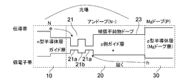
- FIG. 2 is a view schematically showing an energy band in the vicinity of the active layer in the layer structure of the semiconductor light emitting device according to the present embodiment.
- FIG. 3 is a schematic cross-sectional view showing a semiconductor light emitting device according to one embodiment.
- FIG. 4 shows a crystal structure of a nitride semiconductor, for example, showing a form in which the major surface of the crystal is one of semipolar planes.
- FIG. 5 is a graph showing simulation results of the thickness and operating voltage of the p-side guide layer when the residual donor level in the p-side guide layer is changed.
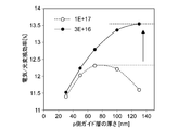
- FIG. 6 is a graph showing simulation results of the electric-light conversion efficiency in the simulation of FIG.
- magnesium (Mg) is the only acceptor dopant material that has been commercialized. It is considered that Mg has a low activation rate and needs to be doped about 100 times the actual carrier density. Since Mg also serves as a light absorption source, if the doping amount is large, the luminous efficiency may be reduced.
- the Mg doped layer As one specific method, it is conceivable to form the Mg doped layer at a certain physical distance or more away from the active layer.
- an intermediate layer is formed in the region by not intentionally doping the acceptor at the time of manufacturing the semiconductor light emitting device. . Because there is residual donor in such an intermediate layer, this intermediate layer is n-type.
- the operating voltage becomes high. This rise in operating voltage occurs because the injection of holes from the p-type side is inhibited.
- the ease of hole injection largely depends on the distance from the electrode side to the active layer in the semiconductor layer and the concentration of the residual donor. Residual donors are considered to be caused by residual impurities and nitrogen vacancies of donor nature, and vary greatly depending on the type of substrate, the plane orientation of the substrate, growth conditions, and the like.
- FIGS. 1A and 1B schematically show energy bands of the semiconductor light emitting element in the vicinity of the active layer, and show that the injection of holes is hindered.
- the semiconductor light emitting device has a layer structure as shown in FIGS. 1A and 1B.
- the layer structure includes, from the left side, an n-type semiconductor layer 10, an intermediate layer 20 having an active layer 21, and a p-type semiconductor layer 30.
- the active layer 21 has a well layer (for example, multiple). When a plurality of well layers 21a are provided, a barrier layer 21b is provided between them.
- the p-type semiconductor layer 30 is configured as a Mg-doped layer doped with Mg.
- the region between the active layer 21 and the p-type semiconductor layer 30 is hereinafter referred to as “p-side guide layer 23” for the convenience of description.
- the intermediate layer 20 including the p-side guide layer 23 is only n-type due to the presence of the residual donor as described above. This residual donor is indicated by "+" in the figure.
- the donor (residual donor) emits one free electron. Free electrons can move freely according to the bias state. As a result, in the p-side guide layer 23, the electrical polarity of the donor which has emitted free electrons becomes "+".
- FIG. 1B shows that most of the holes do not reach the active layer 21 when the distance of the p-side guide layer 23 is larger than that of FIG. Specifically, in order for holes to reach the well layer of the active layer 21 from the p-type semiconductor layer 30, the p-type guide layer 23 resists the repulsion of the positive donor remaining in the p-side It is necessary to get over the side guide layer 23. In this case, a large bias is required, which is considered to be a factor to increase the operating voltage.
- examples of sources of residual donors include residual oxygen, nitrogen vacancies, and the like.
- it is necessary to greatly change the growth conditions and to improve the growth method itself, and it is difficult to improve it to obtain satisfactory characteristics.
- the present technology employs, as a method of reducing the concentration of residual donor, a method of doping an impurity that suppresses the function of residual donor instead of directly excluding its origin.
- suppressing the function of the residual donor may be referred to as “compensating the residual donor”.
- At least one of carbon (C), iron (Fe), zinc (Zn), and the like is used as an impurity for compensating for the residual donor (hereinafter referred to as “compensation impurity” for convenience).
- At least one of beryllium (Be), calcium (Ca), and barium (Ba) is used as a group 2 element instead of (or in addition to) at least one of C, Fe, and Zn described above. May be Alternatively, instead of (or in addition to) at least one of these elements, at least one of titanium (Ti) and zirconium (Zr) may be used as a group 4 element, for example.
- FIG. 2 is a view schematically showing an energy band in the vicinity of the active layer 21 in the layer structure of the semiconductor light emitting device according to the present embodiment.
- the crystal growth conditions are changed and additional source gas is added to the region to be compensated (the p-side guide layer 23).
- the p-type semiconductor layer 30 and the intermediate layer 20 are formed such that the concentration of the compensation impurity in the p-side guide layer 23 is higher than that of the p-type semiconductor layer 30.
- the p-type semiconductor layer 30 may not contain the compensation impurity. That is, in this case, the concentration of the compensation impurity in the p-type semiconductor layer 30 is zero. However, when the semiconductor light emitting device is manufactured, when the compensation impurity is doped to the intermediate layer 20, a slight amount of the compensation impurity which is not intended by the manufacturer may be also doped to the p-type semiconductor layer 30.
- the function of the residual donor of the p-side guide layer 23 is suppressed. That is, the concentration of residual donors with + polarity which gives the holes repulsive force is reduced. As a result, as shown in FIG. 2, even if the p-side guide layer 23 is thick, that is, the p-type semiconductor layer 30 is provided apart from the active layer 21 by a certain amount or more, the p-type semiconductor layer 30 to the active layer 21 Holes are more likely to be injected.
- FIG. 3 is a schematic cross-sectional view showing a semiconductor light emitting device according to one embodiment.
- the semiconductor light emitting device 1 is, for example, a nitride semiconductor laser (LD).
- the nitride semiconductor is a compound semiconductor containing a nitrogen (N) element and containing at least one element of aluminum (Al), gallium (Ga), and indium (In).
- the LD has a structure in which the semiconductor layer 100 is provided on the substrate 50 and the semiconductor layer 100 is sandwiched between a pair of resonator end faces, and is an end face light emitting semiconductor laser.
- the nitride semiconductor LD has a semiconductor layer 100 formed on the side of the first major surface 51 of the substrate 50.
- the semiconductor layer 100 includes, for example, the first cladding layer 12, the first guide layer 14, the active layer 21, the second guide layer 23 ′, the carrier block layer 25, the second cladding layer 30 ′, and the p-contact from the substrate 50 side.
- the layers 32 are formed and configured in order.
- the second guide layer 23 ′ corresponds to the p-side guide layer 23.
- the “layer structure” according to the present technology substantially corresponds to the structure from the first cladding layer 12 to the second cladding layer 30 ′ (or the p-contact layer 32).
- a first electrode layer 61 is formed on the side of the second major surface 52 opposite to the side of the first major surface 51 of the substrate 50.
- a second electrode layer 62 is formed on the surface of the p-contact layer 32.
- the semiconductor layer 100 has a convex ridge 30a.
- An insulating film 40 is formed on the second cladding layer 30 ′ and the semiconductor layer 100 in the ridge portion 30a.
- the main constituent material of the substrate 50 is, for example, GaN, AlN, Al 2 O 3 (sapphire), SiC, Si, or ZrO.
- a typical example of this embodiment is GaN.
- the main surface of the GaN substrate crystal may be any of a polar surface, a semipolar surface, and a nonpolar surface.
- the main surface is a surface on which a crystal grows.
- Polarity means the degree to which polarization occurs and an electric field occurs, that is, the piezoelectric effect occurs. Piezoelectric effects are likely to occur in the polar plane and are less likely to occur in the nonpolar plane.
- Polar planes can be represented as ⁇ 0,0,0,1 ⁇ , ⁇ 0,0,0, -1 ⁇ , for example, using surface indices.
- Semipolar planes are, for example, ⁇ 2, 0, -2, 1 ⁇ , ⁇ 1, 0, -1, 1 ⁇ , ⁇ 2, 0, -2, -1 ⁇ , ⁇ 1, 0, -1, -1 ⁇ It can be expressed as.
- Nonpolar planes can be represented, for example, as ⁇ 1, 1, -2, 0 ⁇ , ⁇ 1, -1, 0, 0 ⁇ .
- "-" represents the bar above the numbers.
- ⁇ 2, 0, -2, 1 ⁇ is the crystal plane of the main surface.
- the plane orientation of ⁇ 2, 0, ⁇ 2, 1 ⁇ has an inclination with respect to both the c and m axes. Specifically, the inclination of the surface of ⁇ 2, 0, -2, 1 ⁇ is 75 ° with respect to the m axis.
- a plane orientation (an axis perpendicular to a plane) has an inclination with respect to a particular axis” means that the plane and the particular axis are nonparallel and nonperpendicular.
- the first cladding layer 12 is formed on the first major surface 51 of the substrate 50, and is made of, for example, at least one of a GaN layer having n-type conductivity, an AlGaN layer, and an AlGaInN layer.
- Si can be used as a dopant for obtaining n-type conductivity.
- the film thickness of the first cladding layer 12 is, for example, 500 nm or more and 3000 nm or less.
- the first guide layer 14 is formed on the first cladding layer 12 and is made of, for example, at least one of a GaN layer having n-type conductivity, an InGaN layer, and an AlGaInN layer.
- a GaN layer having n-type conductivity for example, Si can be used as a dopant for obtaining n-type conductivity.
- the first guide layer 14 may be a non-doped layer.
- the film thickness of the first guide layer 14 is, for example, 10 nm or more and 500 nm or less.
- the active layer 21 is formed by laminating, for example, a well layer and a barrier layer on the first guide layer 14 as described above.
- the well layer is made of, for example, an InGaN layer having n-type conductivity.
- Si can be used as a dopant for obtaining n-type conductivity.
- the well layer may be a non-doped layer.
- the film thickness of the well layer is, for example, 1 nm or more and 100 nm or less.
- the photon wavelength generated in the active layer 21 is, for example, 480 nm or more and 550 nm or less.
- the barrier layer is made of, for example, a GaN layer having n-type conductivity, an InGaN layer, an AlGaN layer, or an AlGaInN layer.
- Si can be used as a dopant for obtaining n-type conductivity, or the barrier layer may be a non-doped layer.
- the film thickness of the barrier layer is, for example, 1 nm or more and 100 nm or less.
- the band gap of the barrier layer is formed to be equal to or larger than the band gap which is the largest in the well layer.
- the second guide layer 23 ′ is formed on the active layer 21 and is made of, for example, at least one of a GaN layer having n-type conductivity, an InGaN layer, and an AlGaInN layer.
- the film thickness of the second guide layer 23 ′ is, for example, 10 nm or more and 500 nm or less.
- a dopant for obtaining n-type conductivity is not included, but a slight amount is possible.
- Si can be used as a dopant, for example.
- the second guide layer 23 ' substantially corresponds to the "region between the active layer 21 and its p-type semiconductor layer 30" as described above.
- the second guide layer 23 ′ and the active layer 21 substantially correspond to the “intermediate layer 20”.
- all or part of the second guide layer 23 ′ contains the above-described compensation impurity, and the concentration of the compensation impurity is the concentration of the compensation impurity in the carrier block layer 25 and the second cladding layer 30 ′. Higher than.
- the compensating impurity is C
- the concentration is controlled by the addition of C 2 H 2 gas.
- the carrier block layer 25 is formed on the second guide layer 23 ′, and is made of, for example, at least one of a GaN layer having p-type conductivity, an AlGaN layer, and an AlGaInN layer.
- Mg can be used as a dopant for obtaining p-type conductivity.
- the film thickness of the carrier block layer 25 is, for example, 3 nm or more and 100 nm or less.
- the carrier block layer 25 can also be disposed in the second guide layer 23 'or the second cladding layer 30'.
- the second cladding layer 30 ' is formed on the carrier block layer 25 and is made of, for example, at least one of a GaN layer having p-type conductivity, an AlGaN layer, and an AlGaInN layer.
- Mg can be used as a dopant for obtaining p-type conductivity.
- the film thickness of the second cladding layer 30 ′ is, for example, 100 nm or more and 1000 nm or less.
- the p-contact layer 32 is formed on the second cladding layer 30 ′ and is made of, for example, at least one of a p-type conductivity GaN layer, an InGaN layer, an AlGaN layer, and an AlGaInN layer.
- Mg can be used as a dopant for obtaining p-type conductivity.
- the film thickness of the p-contact layer 32 is, for example, 1 nm or more and 100 nm or less.
- the carrier block layer 25, the second cladding layer 30 ′, and the p-contact layer 32 correspond to the p-type semiconductor layer 30.
- the ridge portion 30 a having a convex shape is formed by removing the region from the surface of the p-contact layer 32 to the middle of the second cladding layer 30 ′ by etching on one side surface of the semiconductor layer 100. Ru. The region to be removed by etching may reach the second guide layer 23 ′ or the carrier block layer 25.
- the ridge portion 30a is formed extending in the resonant direction of light (the direction perpendicular to the paper surface in FIG. 3), and its length is, for example, 50 ⁇ m or more and 3000 ⁇ m or less.
- the width of the ridge portion 30 a in the direction perpendicular to the resonance direction and the semiconductor lamination direction is, for example, 0.5 ⁇ m to 100 ⁇ m.
- the insulating film 40 is formed on the semiconductor layer 100 exposed by the formation of the ridge portion 30 a.
- the insulating film 40 is made of, for example, SiO 2 , and the film thickness thereof is, for example, 10 nm or more and 500 nm or less.
- the first electrode layer 61 formed on the second major surface 52 of the substrate 50 is made of, for example, Ti and Al in order from the side closer to the substrate 50.
- the film thickness of the Ti layer is, for example, 5 nm or more and 50 nm or less
- the film thickness of the Al layer is, for example, 10 nm or more and 300 nm or less.
- the second electrode layer 62 formed on the p-contact layer 32 is made of, for example, Pd and Pt in order from the side close to the p-contact layer 32.
- the film thickness of the Pd layer is, for example, 5 nm or more and 50 nm or less, and the film thickness of the Pt layer is, for example, 10 nm or more and 300 nm or less.
- the implantation from the p-type semiconductor layer 30 is performed. Holes can easily reach the active layer 21 through the region between the active layer 21 and the p-type semiconductor layer 30. Thereby, the light conversion efficiency (electricity-light conversion efficiency) is improved. That is, specifically, the distance from the active layer 21 to the p-type semiconductor layer 30 can be increased while suppressing an increase in the operating voltage, thereby suppressing light absorption in the p-type semiconductor layer 30 and internal loss during operation. It can be reduced. As a result, it is possible to improve the light conversion efficiency and the output.
- FIG. 5 is a graph showing simulation results of the thickness and the operating voltage of the p-side guide layer 23 when the residual donor level (remaining donor concentration) in the p-side guide layer 23 is changed.
- the operating voltage shows the case where a constant current of 0.8 A is used. For example, it can be seen that the operating voltage is reduced if the residual donors of 1 ⁇ 10 17 / cm 3 are compensated to reduce to 3 ⁇ 10 16 / cm 3 .
- FIG. 6 is a graph showing simulation results of the electric / light conversion efficiency in the simulation of FIG.
- the thickness of the p-side guide layer 23 is increased (that is, the p-type semiconductor layer 30 is further from the active layer 21), light absorption in the p-type semiconductor layer 30 is suppressed, but the voltage increases.
- the optimum point is shifted to the thicker side of the p-side guide layer 23, and the maximum value of the electric / light conversion efficiency is improved.
- the thickness of the optimum range of the thickness of the p-side guide layer 23 is 60 nm or more and 200 nm or less, preferably 80 nm or more and 180 nm or less, and more preferably 100 nm or more and 160 nm or less. Or more preferably, it is 120 nm or more and 140 nm or less.
- the present technology is particularly effective when the residual donor level is high. This is effective when, for example, the residual donor level is high depending on the plane orientation of the substrate 50, or when there are many donor defects using different substrates such as GaN growth on a Si substrate.
- LD Laser Deformation Deformation
- the present technology can also be configured as follows. (1) an n-type semiconductor layer, a p-type semiconductor layer, A nitride semiconductor layer structure having an active layer, and including an intermediate layer provided between the n-type semiconductor layer and the p-type semiconductor layer, The layer structure includes a residual donor in at least a region of the intermediate layer between the active layer and the p-type semiconductor layer, The intermediate layer includes an impurity for compensating for the residual donor in a region between the active layer and the p-type semiconductor layer, and the concentration of the impurity in the region between the active layer and the p-type semiconductor layer is A semiconductor light emitting device configured to have a concentration higher than the concentration of the impurity in the p-type semiconductor layer.
- the semiconductor light emitting device according to (1) above, The p-type semiconductor layer is a layer containing magnesium as an acceptor.
- the semiconductor light emitting device according to (5) above, The substrate is made of gallium nitride, The surface orientation of the main surface of the substrate on which the layer structure is formed is inclined with respect to both the c and m axes.
Landscapes
- Physics & Mathematics (AREA)
- Condensed Matter Physics & Semiconductors (AREA)
- General Physics & Mathematics (AREA)
- Electromagnetism (AREA)
- Optics & Photonics (AREA)
- Geometry (AREA)
- Semiconductor Lasers (AREA)
- Led Devices (AREA)
Abstract
半導体発光素子は、窒化物半導体の層構造を備え、前記層構造は、n型半導体層と、p型半導体層と、中間層とを含む。前記中間層は、活性層を有し、前記n型半導体層および前記p型半導体層の間に設けられる。前記層構造は、少なくとも前記中間層のうち、前記活性層と前記p型半導体層との間の領域に残留ドナーを含む。前記中間層は、前記活性層と前記p型半導体層との間の領域に前記残留ドナーを補償する不純物を含む。そして、前記中間層は、前記活性層と前記p型半導体層との間の領域における前記不純物の濃度が、前記p型半導体層における前記不純物の濃度より高くなるように構成される。
Description
本技術は、LD(Laser Diode)やLED(Light Emitting Diode)といった半導体発光素子に関する。
半導体レーザは、多くの分野において利用されている。例えば光の三原色である赤、緑、青色光を発生する半導体レーザが全て実現されたことにより、小型、低消費電力といった特長を活かし、TVやプロジェクタといった映像表示装置への応用が期待される。
特許文献1に記載の半導体光デバイスは、n型を有する第1化合物半導体層、活性層、および、p型を有する第2化合物半導体層から成る積層構造体を備える。活性層は、少なくとも3層の障壁層、および、障壁層によって挟まれた井戸層を有する。それら障壁層のバンドギャップエネルギー値が適切に設計されることにより、電子オーバーフロー抑制が抑制される(例えば、特許文献1参照。)。
現在、特に、青、緑色光を発生する窒化物半導体を利用した半導体発光素子のさらなる出力や効率の向上が求められている。
本開示の目的は、窒化物半導体を利用する半導体発光素子の特性を向上させることにある。
一形態に係る半導体発光素子は、窒化物半導体の層構造を備え、前記層構造は、n型半導体層と、p型半導体層と、中間層とを含む。
前記中間層は、活性層を有し、前記n型半導体層および前記p型半導体層の間に設けられる。
前記層構造は、少なくとも前記中間層のうち、前記活性層と前記p型半導体層との間の領域に残留ドナーを含む。
前記中間層は、前記活性層と前記p型半導体層との間の領域に前記残留ドナーを補償する不純物を含む。そして、前記中間層は、前記活性層と前記p型半導体層との間の領域における前記不純物の濃度が、前記p型半導体層における前記不純物の濃度より高くなるように構成される。
前記中間層は、活性層を有し、前記n型半導体層および前記p型半導体層の間に設けられる。
前記層構造は、少なくとも前記中間層のうち、前記活性層と前記p型半導体層との間の領域に残留ドナーを含む。
前記中間層は、前記活性層と前記p型半導体層との間の領域に前記残留ドナーを補償する不純物を含む。そして、前記中間層は、前記活性層と前記p型半導体層との間の領域における前記不純物の濃度が、前記p型半導体層における前記不純物の濃度より高くなるように構成される。
中間層が、残留ドナーを抑制する不純物を含むので、p型半導体層から注入されるホールが、活性層とp型半導体層との間の領域を介して活性層に到達しやすくなる。これにより、光変換効率が向上する。
前記p型半導体層は、アクセプタとしてマグネシウムを含む層であってもよい。
前記不純物は、炭素、鉄、および亜鉛のうち少なくとも1つであってもよい。
前記不純物は、2族および4族の元素のうち少なくとも1つであってもよい。
前記半導体発光素子は、前記層構造が形成される基板をさらに具備してもよい。
前記基板の主構成材料は、窒化ガリウム、窒化アルミニウム、サファイア、またはシリコンであってもよい。
前記基板の主構成材料は、窒化ガリウム、窒化アルミニウム、サファイア、またはシリコンであってもよい。
前記基板は、窒化ガリウムで構成され、前記基板の前記層構造が形成される主面の面方位は、cおよびm軸の両方に対して傾きを有していてもよい。
以上、本技術によれば、窒化物半導体を利用する半導体発光素子の特性を向上させることができる。
なお、ここに記載された効果は必ずしも限定されるものではなく、本開示中に記載されたいずれかの効果であってもよい。
以下、本技術に係る実施形態を、図面を参照しながら説明する。
1.本技術の概要
窒化物系の材料、特にAlGaInN系材料では、マグネシウム(Mg)が実用化されている唯一のアクセプタのドーパント材料である。Mgは、活性化率が低く、実際のキャリア密度の100倍程度をドーピングする必要があると考えられる。Mgは光吸収源にもなるため、そのドープ量が多いと発光効率が低下するおそれがある。
Mgによる光吸収を抑えるには、Mgドープ層と、光場(エネルギーバンド図での光強度分布)との重なりを減らすことが必要である。
具体的な一つの方法として、活性層から、ある一定以上の物理的な距離をあけてMgのドープ層を形成することが考えられる。この場合、半導体発光素子の製造時において、活性層からMgドープ層(つまりp型半導体層)までの間の領域では、アクセプタを意図的にドープしないことにより、当該領域に中間層が形成される。かかる中間層には残留ドナーが存在するため、この中間層はn型になる。
Mgドープ層の位置を活性層から物理的に一定以上離した場合に、動作電圧が高くなる。この動作電圧の上昇は、p型側からのホールの注入が阻害されるために起こる。ホールの注入の容易性は、半導体層において電極側から活性層までの距離と、残留ドナーの濃度に大きく依存する。残留ドナーは、ドナー性の残留不純物や窒素空孔が原因と考えられており、基板の種類、基板の面方位、成長条件等に依存して、大きく変動する。
図1A、Bは、活性層近傍の半導体発光素子のエネルギーバンドを模式的に示す図であり、ホールの注入が妨げられる様子を示す。
半導体発光素子は、図1A、Bに示すように層構造を備える。層構造は、左側から、n型半導体層10と、活性層21を有する中間層20と、p型半導体層30とを含む。図1A、Bに示す例では、活性層21は井戸層(例えば複数)を有する。複数の井戸層21aが設けられる場合、それらの間に障壁層21bが設けられる。
p型半導体層30は、MgがドープされたMgドープ層として構成される。活性層21とそのp型半導体層30との間の領域を、以下では説明の便宜上、「p側ガイド層23」と称する。このp側ガイド層23を含む中間層20は、上述したように残留ドナーの存在により、あくまでn型である。この残留ドナーを図中、「+」で示す。
なお、ドナー(残留ドナー)は1つの自由電子を放出する。自由電子は、バイアス状態にしたがって自由に動くことができる。その結果、p側ガイド層23では、自由電子を放出したドナーの電気極性は「+」になる。
図1Aは、p側ガイド層23の距離(活性層21からp型半導体層30までの距離)が小さいため、p型半導体層30と光場との重なりがあり、Mgによる光の吸収が起こることを示す。
図1Bは、上記p側ガイド層23の距離を、図1Aのそれに比べ大きく一定以上とした場合、ほとんどのホールが活性層21まで届かないことを示す。具体的には、ホールが、p型半導体層30から活性層21の井戸層に到達するためには、上記p側ガイド層23に含まれる+極性の残留ドナーの反発に抗して、このp側ガイド層23を乗り越える必要がある。この場合、大きなバイアスを必要とし、これが動作電圧を上げる要因となると考えられる。
これらを解決する手段として、残留ドナーの濃度を下げることが有効である。一般には、残留ドナーの起源としては、上記したように、残留酸素、窒素空孔等が挙げられる。しかし、これらを制御するには、成長条件の大幅な変更や、成長方法自体の改善が必要となり、満足できる特性を得られるような改善は困難である。
本技術は、残留ドナーの濃度を下げる方法として、直接その起源を除く代わりに、残留ドナーの機能を抑制する不純物をドープする方法を採用する。以下では、残留ドナーの機能を抑制することを、「残留ドナーを補償する」と言う場合もある。
2.実施形態
2.1)半導体発光素子の構成
残留ドナーを補償する不純物(以下、便宜的に「補償不純物」と言う)としては、炭素(C)、鉄(Fe)、および亜鉛(Zn)等のうち少なくとも1つが用いられる。
あるいは、上記C、Fe、Znのうち少なくとも1つに代えて(または加えて)、2族元素として、例えばベリリウム(Be)、カルシウム(Ca)、およびバリウム(Ba)のうち少なくとも1つが用いられてもよい。あるいは、それらの元素のうち少なくとも1つに代えて(または加えて)、4族元素として、例えばチタン(Ti)、およびジルコニウム(Zr)のうち少なくとも1つが用いられてもよい。
図2は、本実施形態に係る半導体発光素子の層構造のうち、活性層21近傍のエネルギーバンドを模式的に示す図である。
本実施形態では、p側ガイド層23の補償不純物の濃度を高める方法として、次のような方法がある。半導体発光素子の製造時において、その補償対象の領域(p側ガイド層23)について、結晶の成長条件の変更や、追加の原料ガスの添加を行う。これにより、p側ガイド層23の補償不純物の濃度が、p型半導体層30のそれより高くなるように、p型半導体層30および中間層20が形成される。
p型半導体層30は、補償不純物を含まない場合もあり得る。つまりその場合、p型半導体層30における補償不純物の濃度は0となる。ただし、半導体発光素子の製造時において、中間層20への補償不純物のドープ時に、製造主の意図しない微量の補償不純物が、p型半導体層30にもドープされる場合がある。
補償不純物がドープされることにより、p側ガイド層23の残留ドナーの機能が抑制される。すなわち、ホールに反発力を与える+極性を持つ残留ドナーの濃度が低下する。その結果、図2に示すように、p側ガイド層23が厚く、つまり活性層21からp型半導体層30が一定以上離れて設けられていても、p型半導体層30から活性層21へのホールが注入されやすくなる。
図3は、一実施形態に係る半導体発光素子を示す模式的な断面図である。この半導体発光素子1は、例えば窒化物系の半導体レーザ(LD)である。ここでの窒化物半導体とは、窒素(N)元素を含み、またアルミニウム(Al)、ガリウム(Ga)、インジウム(In)のうち少なくとも1つの元素を含んで構成された化合物半導体である。
なお、LDは、基板50上に半導体層100を備え、半導体層100を一対の共振器端面によって挟み込んだ構造となっており、端面光出射型の半導体レーザである。
図3に示すように、窒化物半導体のLDは、基板50の第1主面51側に半導体層100が形成されてなる。半導体層100は、基板50側から、例えば第1クラッド層12、第1ガイド層14、活性層21、第2ガイド層23'、キャリアブロック層25、第2クラッド層30'、およびp-コンタクト層32が順に形成されて構成されている。第2ガイド層23'は、上記p側ガイド層23に相当する。
本技術に係る「層構造」は、実質的には、上記第1クラッド層12から第2クラッド層30'(あるいはp-コンタクト層32)までの構造に相当する。
基板50の上記第1主面51側の反対側である第2主面52側には、第1電極層61が形成されている。そしてp-コンタクト層32の表面には第2電極層62が形成されている。半導体層100は、凸状のリッジ部30aを有する。第2クラッド層30'上およびリッジ部30aの半導体層100上には、絶縁膜40が形成されている。
基板50の主構成材料は、例えば、GaN、AlN、Al2O3(サファイア)、SiC、Si、またはZrOである。本実施形態の典型例はGaNである。
GaN基板の結晶の主面は、極性面、半極性面、非極性面のいずれでもよい。主面とは、結晶が成長する面である。極性とは、分極が起こり電界が生じる、つまりピエゾ効果が生じる程度を意味する。極性面ではピエゾ効果が生じやすく、非極性面では生じにくい。
極性面は、例えば面指数を用いて{0,0,0,1}、{0,0,0,-1}と表すことができる。半極性面は、例えば{2,0,-2,1}、{1,0,-1,1}、{2,0,-2,-1}、{1,0,-1,-1}と表すことができる。非極性面は、例えば{1,1,-2,0}、{1,-1,0,0}と表すことができる。ここで「-」は数字の上部のバーを表すものとする。
本技術の適用として効果が高いのは、{2,0,-2,1}を主面の結晶面とする場合である。図4に示すように、基板50がGaNで構成される場合、{2,0,-2,1}の面方位は、cおよびm軸の両方に対して傾きを有する。具体的には、{2,0,-2,1}の面の傾きは、m軸に対して75°である。
なお、「面方位(面に垂直な軸)が特定の軸に対して傾きを有する」とは、その面とその特定の軸とが非平行および非垂直であることを意味する。
第1クラッド層12は、基板50の第1主面51上に形成されており、例えばn型導電性を有するGaN層、AlGaN層、およびAlGaInN層のうち少なくとも1層からなる。n型導電性が得られるためのドーパントとして例えばSiを用いることができる。第1クラッド層12の膜厚は、例えば500nm以上3000nm以下である。
第1ガイド層14は、第1クラッド層12上に形成されており、例えばn型導電性を有するGaN層、InGaN層、およびAlGaInN層のうち少なくとも1層からなる。n型導電性が得られるためのドーパントとして例えばSiを用いることができる。または、第1ガイド層14はノンドープ層であってもよい。第1ガイド層14の膜厚は、例えば10nm以上500nm以下である。
活性層21は、第1ガイド層14上に、上述したように例えば井戸層および障壁層が積層されて形成されている。
井戸層は、例えばn型導電性を有するInGaN層からなる。n型導電性が得られるためのドーパントとして例えばSiを用いることができる。または、井戸層は、ノンドープ層でもよい。井戸層の膜厚は例えば1nm以上100nm以下である。本実施形態では、活性層21で生成される光子波長は、例えば480nm以上550nm以下である。
障壁層は、例えばn型導電性を有するGaN層、InGaN層、AlGaN層、またはAlGaInN層からなる。n型導電性が得られるためのドーパントとして例えばSiを用いることができるし、または、障壁層はノンドープ層でもよい。障壁層の膜厚は例えば1nm以上100nm以下である。なお、障壁層のバンドギャップは井戸層内で最大となるバンドギャップ以上になるように形成されている。
井戸層と障壁層とは交互に隣接して設けられ、井戸層数mはm≧1を満足し、m=1の場合は障壁層は存在しない。本実施形態においてはm=2(図2参照)である。
第2ガイド層23'は、活性層21上に形成されており、例えばn型導電性を有するGaN層、InGaN層、およびAlGaInN層のうち少なくとも1層からなる。第2ガイド層23'の膜厚は、例えば10nm以上500nm以下である。n型導電性が得られるためのドーパントは基本的には含まないが、微量であれば可能である。この場合、ドーパントして例えばSiを用いることができる。
第2ガイド層23'は、実質的には、上述したように「活性層21とそのp型半導体層30との間の領域」に相当する。また、実質的には第2ガイド層23'および活性層21が、「中間層20」に相当する。本技術の特徴として、第2ガイド層23'の全部または一部に、上述の補償不純物を含み、その補償不純物の濃度が、キャリアブロック層25および第2クラッド層30'における当該補償不純物の濃度よりも高い。例えば補償不純物がCの場合、C2H2ガスの添加により、その濃度が制御される。
キャリアブロック層25は、第2ガイド層23'上に形成されており、例えばp型導電性を有するGaN層、AlGaN層、AlGaInN層のうち少なくとも1層からなる。p型導電性が得られるためのドーパントとして例えばMgを用いることができる。キャリアブロック層25の膜厚は、例えば3nm以上100nm以下である。キャリアブロック層25は、第2ガイド層23'や第2クラッド層30'内に配置することもできる。
第2クラッド層30'は、キャリアブロック層25上に形成されており、例えばp型導電性を有するGaN層、AlGaN層、AlGaInN層のうち少なくとも1層からなる。p型導電性が得られるためのドーパントとして例えばMgを用いることができる。第2クラッド層30'の膜厚は、例えば100nm以上1000nm以下である。
p-コンタクト層32は、第2クラッド層30'上に形成されており、例えばp型導電性を有するGaN層、InGaN層、AlGaN層、AlGaInN層のうち少なくとも1層からなる。p型導電性が得られるためのドーパントとして例えばMgを用いることができる。またp-コンタクト層32の膜厚は、例えば1nm以上100nm以下である。
キャリアブロック層25、第2クラッド層30'、およびp-コンタクト層32は、p型半導体層30に相当する。
本実施形態では、半導体層100の一側面において、p-コンタクト層32の表面から第2クラッド層30'の中腹にかけての領域がエッチングで除去されることにより、凸状のリッジ部30aが形成される。なお、エッチングにより除去される領域は、第2ガイド層23'やキャリアブロック層25に達していてもよい。
リッジ部30aは、光の共振方向(図3において紙面垂直方向)に延伸して形成されており、その長さは例えば50μm以上3000μm以下である。また、共振方向および半導体積層方向に対し垂直方向におけるリッジ部30aの幅は、例えば0.5μm以上100μm以下である。
リッジ部30aの形成により露出した半導体層100上には絶縁膜40が形成されている。絶縁膜40は、例えばSiO2からなり、またその膜厚は、例えば10nm以上500nm以下である。
基板50の第2主面52上に形成された第1電極層61は、例えば基板50に近い側から順にTiおよびAlで構成される。Ti層の膜厚は例えば5nm以上50nm以下、Al層の膜厚は例えば10nm以上300nm以下である。
p-コンタクト層32上に形成された第2電極層62は、例えばp-コンタクト層32に近い側から順にPdおよびPtで構成される。Pd層の膜厚は例えば5nm以上50nm以下、Pt層の膜厚は例えば10nm以上300nm以下である。
2.2)効果
以上のように、本実施形態では、中間層20のうちの一部(例えば第2ガイド層23')が、残留ドナーを補償する不純物である補償不純物を含むので、p型半導体層30から注入されるホールが、活性層21とp型半導体層30との間の領域を介して活性層21に到達しやすくなる。これにより、光変換効率(電気-光変換効率)が向上する。すなわち具体的には、動作電圧の上昇を抑制しつつ、活性層21からp型半導体層30までの距離を大きくできることで、p型半導体層30での光吸収を抑え、動作時の内部ロスを低減させることができる。その結果として、光変換効率の改善、出力の向上が可能となる。
図5は、p側ガイド層23における残留ドナーレベル(残留ドナー濃度)を変えた場合の、p側ガイド層23の厚さおよび動作電圧をシミュレーションした結果を示すグラフである。動作電圧は、0.8Aの一定電流を用いた場合を示す。例えば1×10¹⁷個/cm3の残留ドナーが補償されて、3×1016個/cm3に抑えられる場合、動作電圧が低減することがわかる。
また、図6は、図5のシミュレーションにおいて、電気/光変換効率のシミュレーション結果を示すグラフである。p側ガイド層23を厚くする(すなわちp型半導体層30が活性層21から遠くなる)ほど、p型半導体層30での光吸収が抑制されるが、電圧は上昇するため、トレードオフとなり、電気/光変換効率の最適ポイントが存在する。p側ガイド層23の残留ドナーレベルが抑制されるほど、その最適ポイントはp側ガイド層23が厚い側にシフトして、電気/光変換効率の最高値が改善する。
図6より、p側ガイド層23の厚さの最適範囲の厚さは、60nm以上200nm以下、好ましくは80nm以上180nm以下、さらに好ましくは100nm以上160nm以下である。あるいはさらに好ましくは、120nm以上140nm以下である。
以上のように、本技術は、残留ドナーレベルが高い場合に特に有効である。基板50の面方位によって、残留ドナーレベルが高くなる場合や、Si基板上のGaN成長のように異種の基板を用いて、ドナー性欠陥が多い場合等に有効となる。
3.変形例
本技術は、以上説明した実施形態に限定されず、他の種々の実施形態を実現することができる。例えば上記実施形態では、LDを例に挙げたが、これに限られず、LED、SLD(Super Luminescent Diode)、半導体光増幅器等にも本技術を適用可能である。
以上説明した各形態の特徴部分のうち、少なくとも2つの特徴部分を組み合わせることも可能である。
なお、本技術は以下のような構成もとることができる。
(1)
n型半導体層と、
p型半導体層と、
活性層を有し、前記n型半導体層および前記p型半導体層の間に設けられた中間層と
を含む、窒化物半導体の層構造を備え、
前記層構造は、少なくとも前記中間層のうち、前記活性層と前記p型半導体層との間の領域に残留ドナーを含み、
前記中間層は、前記活性層と前記p型半導体層との間の領域に前記残留ドナーを補償する不純物を含み、前記活性層と前記p型半導体層との間の領域における前記不純物の濃度が、前記p型半導体層における前記不純物の濃度より高くなるように構成される
半導体発光素子。
(2)
前記(1)に記載の半導体発光素子であって、
前記p型半導体層は、アクセプタとしてマグネシウムを含む層である
半導体発光素子。
(3)
前記(1)または(2)に記載の半導体発光素子であって、
前記不純物は、炭素、鉄、および亜鉛のうち少なくとも1つ
半導体発光素子。
(4)
前記(1)または(2)に記載の半導体発光素子であって、
前記不純物は、2族および4族の元素のうち少なくとも1つである
半導体発光素子。
(5)
前記(1)から(4)のいうちいずれか1項に記載の半導体発光素子であって、
前記層構造が形成される基板をさらに具備し、
前記基板の主構成材料は、窒化ガリウム、窒化アルミニウム、サファイア、またはシリコンである
半導体発光素子。
(6)
前記(5)に記載の半導体発光素子であって、
前記基板は、窒化ガリウムで構成され、
前記基板の前記層構造が形成される主面の面方位は、cおよびm軸の両方に対して傾きを有する
半導体発光素子。
(1)
n型半導体層と、
p型半導体層と、
活性層を有し、前記n型半導体層および前記p型半導体層の間に設けられた中間層と
を含む、窒化物半導体の層構造を備え、
前記層構造は、少なくとも前記中間層のうち、前記活性層と前記p型半導体層との間の領域に残留ドナーを含み、
前記中間層は、前記活性層と前記p型半導体層との間の領域に前記残留ドナーを補償する不純物を含み、前記活性層と前記p型半導体層との間の領域における前記不純物の濃度が、前記p型半導体層における前記不純物の濃度より高くなるように構成される
半導体発光素子。
(2)
前記(1)に記載の半導体発光素子であって、
前記p型半導体層は、アクセプタとしてマグネシウムを含む層である
半導体発光素子。
(3)
前記(1)または(2)に記載の半導体発光素子であって、
前記不純物は、炭素、鉄、および亜鉛のうち少なくとも1つ
半導体発光素子。
(4)
前記(1)または(2)に記載の半導体発光素子であって、
前記不純物は、2族および4族の元素のうち少なくとも1つである
半導体発光素子。
(5)
前記(1)から(4)のいうちいずれか1項に記載の半導体発光素子であって、
前記層構造が形成される基板をさらに具備し、
前記基板の主構成材料は、窒化ガリウム、窒化アルミニウム、サファイア、またはシリコンである
半導体発光素子。
(6)
前記(5)に記載の半導体発光素子であって、
前記基板は、窒化ガリウムで構成され、
前記基板の前記層構造が形成される主面の面方位は、cおよびm軸の両方に対して傾きを有する
半導体発光素子。
1…半導体発光素子
10…n型半導体層
20…中間層
21…活性層
23…p側ガイド層
30…p型半導体層
50…基板
100…半導体層
10…n型半導体層
20…中間層
21…活性層
23…p側ガイド層
30…p型半導体層
50…基板
100…半導体層
Claims (6)
- n型半導体層と、
p型半導体層と、
活性層を有し、前記n型半導体層および前記p型半導体層の間に設けられた中間層と
を含む、窒化物半導体の層構造を備え、
前記層構造は、少なくとも前記中間層のうち、前記活性層と前記p型半導体層との間の領域に残留ドナーを含み、
前記中間層は、前記活性層と前記p型半導体層との間の領域に前記残留ドナーを補償する不純物を含み、前記活性層と前記p型半導体層との間の領域における前記不純物の濃度が、前記p型半導体層における前記不純物の濃度より高くなるように構成される
半導体発光素子。 - 請求項1に記載の半導体発光素子であって、
前記p型半導体層は、アクセプタとしてマグネシウムを含む層である
半導体発光素子。 - 請求項1に記載の半導体発光素子であって、
前記不純物は、炭素、鉄、および亜鉛のうち少なくとも1つ
半導体発光素子。 - 請求項1に記載の半導体発光素子であって、
前記不純物は、2族および4族の元素のうち少なくとも1つである
半導体発光素子。 - 請求項1に記載の半導体発光素子であって、
前記層構造が形成される基板をさらに具備し、
前記基板の主構成材料は、窒化ガリウム、窒化アルミニウム、サファイア、またはシリコンである
半導体発光素子。 - 請求項5に記載の半導体発光素子であって、
前記基板は、窒化ガリウムで構成され、
前記基板の前記層構造が形成される主面の面方位は、cおよびm軸の両方に対して傾きを有する
半導体発光素子。
Priority Applications (3)
| Application Number | Priority Date | Filing Date | Title |
|---|---|---|---|
| JP2019557028A JPWO2019106931A1 (ja) | 2017-12-01 | 2018-09-27 | 半導体発光素子 |
| US16/766,469 US20200381898A1 (en) | 2017-12-01 | 2018-09-27 | Semiconductor light-emitting device |
| DE112018006151.5T DE112018006151T5 (de) | 2017-12-01 | 2018-09-27 | Halbleiterlichtemissionsvorrichtung |
Applications Claiming Priority (2)
| Application Number | Priority Date | Filing Date | Title |
|---|---|---|---|
| JP2017-231828 | 2017-12-01 | ||
| JP2017231828 | 2017-12-01 |
Publications (1)
| Publication Number | Publication Date |
|---|---|
| WO2019106931A1 true WO2019106931A1 (ja) | 2019-06-06 |
Family
ID=66663949
Family Applications (1)
| Application Number | Title | Priority Date | Filing Date |
|---|---|---|---|
| PCT/JP2018/035965 Ceased WO2019106931A1 (ja) | 2017-12-01 | 2018-09-27 | 半導体発光素子 |
Country Status (4)
| Country | Link |
|---|---|
| US (1) | US20200381898A1 (ja) |
| JP (1) | JPWO2019106931A1 (ja) |
| DE (1) | DE112018006151T5 (ja) |
| WO (1) | WO2019106931A1 (ja) |
Cited By (2)
| Publication number | Priority date | Publication date | Assignee | Title |
|---|---|---|---|---|
| JP2023031164A (ja) * | 2021-08-24 | 2023-03-08 | ヌヴォトンテクノロジージャパン株式会社 | 窒化物系半導体発光素子 |
| US12191420B2 (en) | 2020-12-24 | 2025-01-07 | Nichia Corporation | Nitride semiconductor light emitting element and method of manufacturing same |
Citations (8)
| Publication number | Priority date | Publication date | Assignee | Title |
|---|---|---|---|---|
| JPH0963962A (ja) * | 1995-08-21 | 1997-03-07 | Matsushita Electric Ind Co Ltd | 結晶成長方法および半導体発光素子 |
| JPH09321389A (ja) * | 1996-03-26 | 1997-12-12 | Toshiba Corp | p型半導体膜および半導体素子 |
| WO2007013257A1 (ja) * | 2005-07-29 | 2007-02-01 | Matsushita Electric Industrial Co., Ltd. | 窒化物系半導体素子 |
| WO2011055774A1 (ja) * | 2009-11-06 | 2011-05-12 | 日本碍子株式会社 | 半導体素子用エピタキシャル基板、半導体素子、および半導体素子用エピタキシャル基板の製造方法 |
| JP2014103384A (ja) * | 2012-11-19 | 2014-06-05 | Genesis Photonics Inc | 窒化物半導体構造及び半導体発光デバイス |
| JP2015159193A (ja) * | 2014-02-24 | 2015-09-03 | ソニー株式会社 | 半導体発光素子およびその製造方法、並びに半導体発光素子用ウエハ |
| JP2016531442A (ja) * | 2013-08-22 | 2016-10-06 | コミッサリア ア レネルジー アトミーク エ オ ゼネルジ ザルタナテイヴ | 活性領域がInNの層を含む発光ダイオード |
| JP2016219587A (ja) * | 2015-05-20 | 2016-12-22 | ソニー株式会社 | 半導体光デバイス |
-
2018
- 2018-09-27 JP JP2019557028A patent/JPWO2019106931A1/ja active Pending
- 2018-09-27 US US16/766,469 patent/US20200381898A1/en not_active Abandoned
- 2018-09-27 DE DE112018006151.5T patent/DE112018006151T5/de not_active Withdrawn
- 2018-09-27 WO PCT/JP2018/035965 patent/WO2019106931A1/ja not_active Ceased
Patent Citations (8)
| Publication number | Priority date | Publication date | Assignee | Title |
|---|---|---|---|---|
| JPH0963962A (ja) * | 1995-08-21 | 1997-03-07 | Matsushita Electric Ind Co Ltd | 結晶成長方法および半導体発光素子 |
| JPH09321389A (ja) * | 1996-03-26 | 1997-12-12 | Toshiba Corp | p型半導体膜および半導体素子 |
| WO2007013257A1 (ja) * | 2005-07-29 | 2007-02-01 | Matsushita Electric Industrial Co., Ltd. | 窒化物系半導体素子 |
| WO2011055774A1 (ja) * | 2009-11-06 | 2011-05-12 | 日本碍子株式会社 | 半導体素子用エピタキシャル基板、半導体素子、および半導体素子用エピタキシャル基板の製造方法 |
| JP2014103384A (ja) * | 2012-11-19 | 2014-06-05 | Genesis Photonics Inc | 窒化物半導体構造及び半導体発光デバイス |
| JP2016531442A (ja) * | 2013-08-22 | 2016-10-06 | コミッサリア ア レネルジー アトミーク エ オ ゼネルジ ザルタナテイヴ | 活性領域がInNの層を含む発光ダイオード |
| JP2015159193A (ja) * | 2014-02-24 | 2015-09-03 | ソニー株式会社 | 半導体発光素子およびその製造方法、並びに半導体発光素子用ウエハ |
| JP2016219587A (ja) * | 2015-05-20 | 2016-12-22 | ソニー株式会社 | 半導体光デバイス |
Cited By (2)
| Publication number | Priority date | Publication date | Assignee | Title |
|---|---|---|---|---|
| US12191420B2 (en) | 2020-12-24 | 2025-01-07 | Nichia Corporation | Nitride semiconductor light emitting element and method of manufacturing same |
| JP2023031164A (ja) * | 2021-08-24 | 2023-03-08 | ヌヴォトンテクノロジージャパン株式会社 | 窒化物系半導体発光素子 |
Also Published As
| Publication number | Publication date |
|---|---|
| US20200381898A1 (en) | 2020-12-03 |
| JPWO2019106931A1 (ja) | 2020-11-26 |
| DE112018006151T5 (de) | 2020-09-03 |
Similar Documents
| Publication | Publication Date | Title |
|---|---|---|
| JP5113330B2 (ja) | 窒化ガリウム半導体発光素子 | |
| JP5963004B2 (ja) | 窒化物半導体発光素子 | |
| JP4924185B2 (ja) | 窒化物半導体発光素子 | |
| JP5409210B2 (ja) | 半導体発光素子 | |
| US8917750B2 (en) | III-nitride semiconductor laser diode | |
| JP2010532926A (ja) | 放射線放出半導体ボディ | |
| JP2011187591A (ja) | 窒化物半導体紫外線発光素子 | |
| JPWO2009078482A1 (ja) | 半導体発光素子 | |
| JP7642553B2 (ja) | 半導体発光素子、及び半導体発光素子の製造方法 | |
| CN101268563A (zh) | 氧化锌类化合物半导体元件 | |
| CN101180743A (zh) | 氮化物半导体发光元件 | |
| JP7005890B2 (ja) | 半導体発光素子、照明装置、ヘッドライト、移動体、イルミネーション装置、映像装置、投射型映像装置及びプロジェクター。 | |
| WO2019106931A1 (ja) | 半導体発光素子 | |
| US8405066B2 (en) | Nitride-based semiconductor light-emitting device | |
| WO2010004974A1 (ja) | 窒化物半導体レーザ素子 | |
| JP6183060B2 (ja) | 半導体発光素子 | |
| JP2016066670A (ja) | 半導体レーザ | |
| US10218152B1 (en) | Semiconductor laser diode with low threshold current | |
| JP2007157765A (ja) | 窒化ガリウム半導体発光素子 | |
| JP2013069795A (ja) | 半導体発光素子 | |
| JP2010080741A (ja) | 半導体発光素子 | |
| JP5344676B2 (ja) | 発光素子用基板および発光素子 | |
| JP2008244360A (ja) | 半導体発光素子 | |
| WO2021172171A1 (ja) | レーザ素子 | |
| WO2015001692A1 (ja) | 半導体発光素子 |
Legal Events
| Date | Code | Title | Description |
|---|---|---|---|
| 121 | Ep: the epo has been informed by wipo that ep was designated in this application |
Ref document number: 18882642 Country of ref document: EP Kind code of ref document: A1 |
|
| ENP | Entry into the national phase |
Ref document number: 2019557028 Country of ref document: JP Kind code of ref document: A |
|
| 122 | Ep: pct application non-entry in european phase |
Ref document number: 18882642 Country of ref document: EP Kind code of ref document: A1 |