WO2019097989A1 - 電力変換装置 - Google Patents
電力変換装置 Download PDFInfo
- Publication number
- WO2019097989A1 WO2019097989A1 PCT/JP2018/040019 JP2018040019W WO2019097989A1 WO 2019097989 A1 WO2019097989 A1 WO 2019097989A1 JP 2018040019 W JP2018040019 W JP 2018040019W WO 2019097989 A1 WO2019097989 A1 WO 2019097989A1
- Authority
- WO
- WIPO (PCT)
- Prior art keywords
- terminal
- bus bar
- semiconductor
- module
- capacitor
- Prior art date
- Legal status (The legal status is an assumption and is not a legal conclusion. Google has not performed a legal analysis and makes no representation as to the accuracy of the status listed.)
- Ceased
Links
Images



































Classifications
-
- H—ELECTRICITY
- H02—GENERATION; CONVERSION OR DISTRIBUTION OF ELECTRIC POWER
- H02M—APPARATUS FOR CONVERSION BETWEEN AC AND AC, BETWEEN AC AND DC, OR BETWEEN DC AND DC, AND FOR USE WITH MAINS OR SIMILAR POWER SUPPLY SYSTEMS; CONVERSION OF DC OR AC INPUT POWER INTO SURGE OUTPUT POWER; CONTROL OR REGULATION THEREOF
- H02M7/00—Conversion of AC power input into DC power output; Conversion of DC power input into AC power output
- H02M7/42—Conversion of DC power input into AC power output without possibility of reversal
- H02M7/44—Conversion of DC power input into AC power output without possibility of reversal by static converters
- H02M7/48—Conversion of DC power input into AC power output without possibility of reversal by static converters using discharge tubes with control electrode or semiconductor devices with control electrode
-
- H—ELECTRICITY
- H05—ELECTRIC TECHNIQUES NOT OTHERWISE PROVIDED FOR
- H05K—PRINTED CIRCUITS; CASINGS OR CONSTRUCTIONAL DETAILS OF ELECTRIC APPARATUS; MANUFACTURE OF ASSEMBLAGES OF ELECTRICAL COMPONENTS
- H05K7/00—Constructional details common to different types of electric apparatus
- H05K7/20—Modifications to facilitate cooling, ventilating, or heating
-
- H—ELECTRICITY
- H10—SEMICONDUCTOR DEVICES; ELECTRIC SOLID-STATE DEVICES NOT OTHERWISE PROVIDED FOR
- H10W—GENERIC PACKAGES, INTERCONNECTIONS, CONNECTORS OR OTHER CONSTRUCTIONAL DETAILS OF DEVICES COVERED BY CLASS H10
- H10W40/00—Arrangements for thermal protection or thermal control
- H10W40/40—Arrangements for thermal protection or thermal control involving heat exchange by flowing fluids
- H10W40/47—Arrangements for thermal protection or thermal control involving heat exchange by flowing fluids by flowing liquids, e.g. forced water cooling
Definitions
- the present disclosure relates to a power conversion device in which a plurality of semiconductor modules containing semiconductor elements and a plurality of cooling pipes for cooling the semiconductor modules are stacked.
- a stacked body As a power conversion device that performs power conversion between DC power and AC power, a stacked body is configured by stacking a plurality of semiconductor modules containing semiconductor elements and a plurality of cooling pipes for cooling the semiconductor modules. Those are known (see Patent Document 1 below).
- the semiconductor element is subjected to switching operation, thereby converting DC power supplied from a DC power source into AC power.
- the semiconductor module When the semiconductor element is subjected to switching operation, the semiconductor module generates heat. Therefore, the semiconductor module is cooled using the cooling pipe.
- the power converter further includes electronic components such as a reactor, a capacitor, and a DC-DC converter. These electronic components are electrically connected to the semiconductor module. When the power converter operates, these electronic components also generate heat. Therefore, in recent years, it has been considered to cool these electronic components.
- electronic components such as a reactor, a capacitor, and a DC-DC converter.
- cooling plate made of a metal plate and having the same shape as the cooling pipe. Then, it has been studied to hold an electronic component between the cooling plate and the cooling pipe, and to radiate heat generated from the electronic component using the cooling plate. This makes it possible to lower the temperature of the electronic component.
- the electronic component can not be sufficiently cooled. That is, even if a simple metal plate is used as the cooling plate, the heat generated from the electronic component can not be sufficiently absorbed. Further, when the cooling plate is formed in the same shape as the cooling pipe, the area of the cooling plate is small, so that a sufficient heat dissipation effect can not be obtained.
- One aspect of the present disclosure is a laminated body (10) in which a plurality of semiconductor modules (2) containing a semiconductor element (20) and a plurality of cooling pipes (3) through which a refrigerant for cooling the semiconductor modules flows are stacked.
- Electronic components (4, 6) electrically connected to the semiconductor module;
- the laminate, the electronic component, and the cooling plate are arranged in the stacking direction of the laminate,
- the cooling plate is connected to the cooling pipe, and an in-plate flow path (310) through which the refrigerant flows is formed in the cooling plate in a direction orthogonal to the stacking direction,
- the cooling plate is in the power converter (1), which has a larger area than the cooling pipe when viewed in the stacking direction.
- the in-plate flow passage through which the refrigerant flows is formed in the cooling plate. Therefore, heat exchange can be performed between the refrigerant flowing in the in-plate flow passage and the electronic component, and the electronic component can be effectively cooled.
- the cooling plate of the power converter has a larger area when viewed from the stacking direction than the cooling pipe. Therefore, the area in which the cooling plate and the electronic component are in thermal contact can be increased, and the electronic component can be efficiently cooled.
- the area of the cooling plate is increased, a large in-plate flow path can be formed in the cooling plate. Therefore, the cooling efficiency of the electronic component can be enhanced.
- the contact area with air is increased, so the heat radiation efficiency of the cooling plate can be enhanced. Therefore, the temperature of the cooling plate can be lowered, and the electronic components can be cooled more efficiently.
- the power converter device which can improve the cooling efficiency of an electronic component more can be provided.
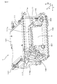
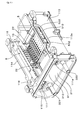
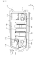
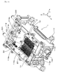
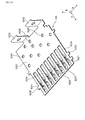
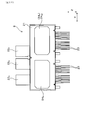
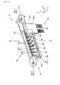
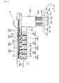
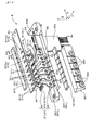
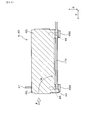
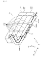
- FIG. 1 is a perspective view of a power conversion device in which a capacitor module or the like is omitted in the embodiment
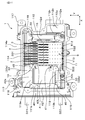
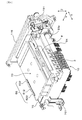
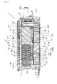
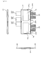
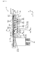
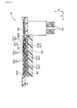
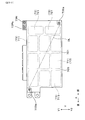
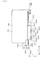
- FIG. 2 is a plan view of the power conversion device in which some parts are omitted in the embodiment
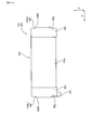
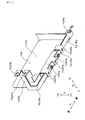
- FIG. 3 is a plan view of the power converter according to a plane perpendicular to the Z direction in the embodiment
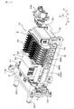
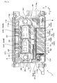
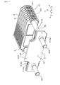
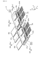
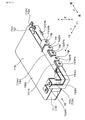
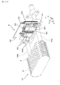
- FIG. 4 is a perspective view of the power conversion device in which the cooling plate and the like are omitted in the embodiment
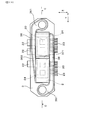
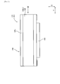
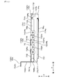
- FIG. 5 is a plan view of the power conversion device in which the case and the like are omitted according to the embodiment
- FIG. 1 is a perspective view of a power conversion device in which a capacitor module or the like is omitted in the embodiment
- FIG. 2 is a plan view of the power conversion device in which some parts are omitted in the embodiment
- FIG. 3 is a plan view of the power converter according to a plane perpendicular to the Z direction in the embodiment
- FIG. 4 is a perspective view of the power conversion device in which the cooling plate
- FIG. 6 is a perspective view of the power conversion device in which the current sensor and the like appear in the embodiment
- FIG. 7 is a perspective view of the power conversion device in which the case and the capacitor module etc. are omitted in the embodiment
- FIG. 8 is a perspective view of a power conversion device in which a capacitor module or the like appears in the embodiment
- FIG. 9 is a perspective view of the power conversion device with the case etc. omitted in the embodiment
- FIG. 10 is another perspective view of the power conversion device in which the case and the like are omitted in the embodiment
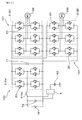
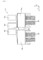
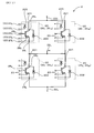
- FIG. 11 is a circuit diagram of the power conversion device in the embodiment
- FIG. 12 is a perspective view of the power conversion device with the lower case cover removed in the embodiment
- FIG. 13 is a perspective view of the power conversion device as viewed obliquely from below with the case etc. omitted in the embodiment;
- FIG. 14 is another perspective view of the power conversion device viewed obliquely from below with the case etc. omitted in the embodiment,
- FIG. 15 is a front view of the power conversion device in which the DC-DC converter appears in the embodiment,
- FIG. 16 is a plan view of the power conversion device according to a plane perpendicular to the Y direction in the embodiment;
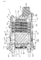
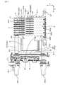
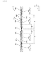
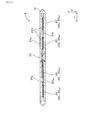
- FIG. 17 is a sectional view taken along line AA of FIG. 18 is a cross-sectional view taken along line B-B in FIG.
- FIG. 19 is a perspective view of the power conversion device with the bottom wall exposed in the embodiment, FIG.
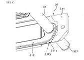
- FIG. 20 is an enlarged perspective view in the vicinity of the engagement claw on the upper side of the cooling plate in the embodiment;
- FIG. 21 is an enlarged perspective view in the vicinity of the engagement claw on the lower side of the cooling plate in the embodiment;
- FIG. 22 is another enlarged perspective view of the upper side near the engagement claw of the cooling plate in the embodiment;
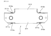
- FIG. 23 is a front view of a cooling plate in an embodiment;
- FIG. 24 is a front view of the case in the embodiment;
- FIG. 25 is a plan view of the case in the embodiment;
- FIG. 26 is a perspective view of a cooler according to the embodiment;
- FIG. 27 is another perspective view of the cooler according to the embodiment;
- FIG. 28 is a front view of a refrigerant flow passage of a cooling pipe in the embodiment;
- FIG. 29 is a front view of a cooling pipe overlapped with a semiconductor module in the embodiment;
- FIG. 30 is a cross-sectional view of a cooling pipe corresponding to a cross section taken along line C-C of FIG. 31 is an exploded cross-sectional view of a cooling pipe in the embodiment,
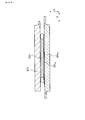
- FIG. 32 is a cross-sectional view of a laminate in the embodiment;
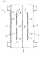
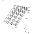
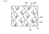
- FIG. 33 is a perspective view of a portion of the inner fin in the embodiment;
- FIG. 34 is a cross-sectional view of a portion of the inner fin, taken along the line DD in FIG. 31;
- FIG. 35 is an enlarged perspective view of a portion of inner fin in the embodiment;
- 36 is a cross-sectional view taken along the line EE of FIG. FIG.
- FIG. 37 is an explanatory diagram of a method of manufacturing a cooler according to the embodiment;
- FIG. 38 is a perspective view of a bus barrier in the embodiment;
- FIG. 39 is a perspective view of the bus barrier in a state in which the mold portion is removed in the embodiment;
- FIG. 40 is a perspective view of the high potential bus bar in the embodiment;
- FIG. 41 is a perspective view of the low potential bus bar in the embodiment;
- FIG. 42 is a plan view of a bus barrier in a state in which the mold portion is removed in the embodiment;
- FIG. 43 is a side view of the bus barrier with the mold portion removed in the embodiment;
- FIG. 44 is a front view of a bus barrier in the embodiment;
- FIG. 45 is a side view of the bus barrier in the embodiment;
- FIG. 46 is a partial cross-sectional view of the bus barrier assembly corresponding to the cross section taken along line F-F in FIG.
- FIG. 47 is a perspective view illustrating the method of manufacturing a bus barrier according to the embodiment
- FIG. 48 is a side view illustrating the method of manufacturing a bus barrier according to the embodiment
- FIG. 49 is a front view illustrating a method of manufacturing a bus barrier according to the embodiment
- FIG. 50 is a perspective view of the bus barrier before removing the holding pin in the embodiment
- FIG. 51 is a perspective view of the inside of the semiconductor module in the embodiment
- FIG. 52 is a perspective view of the semiconductor module in the embodiment
- 53 is a view seen through a part of FIG. 51
- 54 is an exploded perspective view of the inside of the semiconductor module in the embodiment, FIG.
- FIG. 55 is a transparent plan view of the semiconductor module in the embodiment;
- FIG. 56 is a partially transparent plan view of the semiconductor module in the embodiment;
- FIG. 57 is a rear view of the inside of the semiconductor module in the embodiment;
- FIG. 58 is a plan view of the semiconductor module in the embodiment;
- 59 is a cross-sectional view taken along line G1-G1 of FIG. 60 is a cross-sectional view of the semiconductor module in the embodiment, and is a view in which a module main body is added to FIG. 59
- FIG. 61 is an enlarged view of the main part of FIG. 59;
- 62 is an enlarged view of the semiconductor device of FIG. 59;
- 63 is a cross-sectional view taken along line G2-G2 of FIG. FIG.
- FIG. 64 is a cross-sectional view of the semiconductor module in the embodiment, showing the module main body added to FIG. 63.
- FIG. 65 is an enlarged view of an essential part of FIG. 66 is a cross-sectional view taken along line G3-G3 of FIG.
- FIG. 67 is an enlarged view of an essential part of FIG. 66
- 68 is a cross-sectional view taken along line G4-G4 of FIG.
- FIG. 69 is an enlarged view of an essential part of FIG.
- FIG. 70 is a three-sided view of the semiconductor module in the embodiment
- FIG. 71 is a circuit diagram of the semiconductor module in the embodiment
- 72 is a perspective view of the current sensor in the embodiment
- 73 is a view on arrow H1 of FIG.
- FIG. 79 is an exploded perspective view of the current sensor in the embodiment, 80 is an I1-I1 cross-sectional view of FIG. 78; 81 is a cross-sectional view taken along line I2-I2 of FIG.
- FIG. 82 is a perspective view of a reactor case in the embodiment; 83 is a view on arrow J1 of FIG. 82, 84 is a view on arrow J2 in FIG.
- FIG. 89 is a perspective view of a capacitor module in the embodiment
- FIG. 90 is a top view of the capacitor module in the embodiment
- FIG. 91 is a diagram in which the mold resin and the discharge resistance substrate are omitted in FIG. 89
- 92 is a view on arrow K1 of FIG. 91
- FIG. 93 is a view on arrow K2 of FIG. 91
- FIG. 94 is a view of FIG.
- FIG. 95 is a view of the negative electrode bus bar, the positive electrode smooth bus bar, the positive electrode filter bus bar, and the insulating member as viewed from below in the embodiment;
- FIG. 96 is a top view of the negative electrode bus bar, the positive electrode smooth bus bar, the positive electrode filter bus bar, and the insulating member in the embodiment,
- FIG. 97 is a perspective view of a negative electrode bus bar, a positive electrode smooth bus bar, a positive electrode filter bus bar, and an insulating member according to the embodiment, in which the negative electrode bus bar is partially omitted,
- FIG. 98 is a perspective view of a case cover and a capacitor module in the embodiment, FIG.
- FIG. 99 is a schematic cross-sectional view showing a case cover, a capacitor module, a discharge resistance substrate, a reactor, a semiconductor module, and a cooler according to the embodiment.
- FIG. 100 is a perspective view of a stack, a cooling plate, and a DC-DC converter according to the embodiment;
- FIG. 101 is a cross-sectional view of a holding structure of a DC-DC converter according to an embodiment;
- FIG. 102 is a plan view of a holding structure of a DC-DC converter according to an embodiment;
- FIG. 103 is a plan view of a holding structure of the DC-DC converter from which the DDC facing wall is removed according to the embodiment;
- FIG. 100 is a perspective view of a stack, a cooling plate, and a DC-DC converter according to the embodiment;
- FIG. 101 is a cross-sectional view of a holding structure of a DC-DC converter according to an embodiment;
- FIG. 102 is a plan view of a holding structure of a
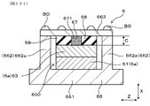
- FIG. 104 is a cross-sectional view of a holding structure of a DC-DC converter showing a modification of the embodiment
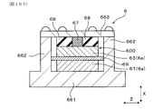
- FIG. 105 is a cross-sectional view of the holding structure (part 1) of the DC-DC converter in the embodiment
- FIG. 106 is a plan view of a holding structure (part 2) of the DC-DC converter from which the DDC facing wall is removed in the embodiment
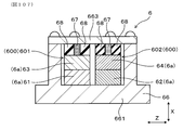
- FIG. 107 is a cross-sectional view of the holding structure (part 3) of the DC-DC converter in the embodiment
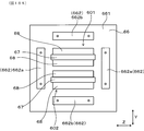
- FIG. 108 is a plan view of a holding structure (part 3) of the DC-DC converter from which the DDC facing wall is removed in the embodiment
- FIG. 109 is a cross-sectional view of the holding structure (part 4) of the DC-DC converter in the embodiment.
- the power converter according to an embodiment of the present disclosure will be described in detail below with reference to the drawings.
- the power conversion device according to the embodiment of the present disclosure takes into consideration the following technical viewpoints in order to meet the needs of the world.
- the power conversion device according to the embodiment of the present disclosure is commercialized based on the three viewpoints described above, and a viewpoint that combines these viewpoints. Moreover, the contents described in the text in the embodiment are one specific example of the technology relating to the above-described technical viewpoint, and the power conversion device according to the embodiment of the present disclosure is outlined above in the above-mentioned technical viewpoint and below.
- the cooling performance is improved by adopting a configuration in which a plurality of power semiconductor modules (simply referred to as “semiconductor modules” as appropriate) are cooled from both sides.
- semiconductor modules semiconductor modules
- a technique of indirect cooling via a heat conduction member such as a cooling pipe wall between a semiconductor module and a refrigerant is described.
- the pressure be uniformly applied between the cooler and the heat dissipation surface of the semiconductor module. This point is particularly important in the case of indirect cooling. In particular, it is important to secure a contact area between the cooler and the semiconductor module as the size of the semiconductor module increases with the increase in power consumption. In the present embodiment, as an example, the contact area is secured by uniformly applying a pressing force in the stacking direction of the cooler and the semiconductor module. That is, it is required to contribute to the improvement of the cooling performance of the semiconductor module by equalizing the pressure. Note that the proportion of the volume occupied by the semiconductor module in the power conversion device is increased not only in the case of the increase in size as a single module but also in the case of dealing with the number of semiconductor modules. Furthermore, with the increase of the allowable current, insulation of the inside of the semiconductor module and heat capacity are ensured, and the configuration of the semiconductor module is likely to be complicated and enlarged.
- the power conversion device of the present embodiment it is also considered to reduce the dead space as much as possible by collecting components in one direction.
- the efficient arrangement of the electrical wiring contributes to the miniaturization of the entire power conversion device.
- securing insulation with other electrical parts and metal parts that is, securing a space insulation distance and securing a creeping surface insulation
- the countermeasure is considered.
- the electrical wiring placed in the dead space simply for miniaturization, but a portion where the optimal arrangement taking into account shortening of the electrical wiring and safety (connection workability, vibration countermeasures in the usage environment, etc.) is also made. There is also.
- the whole layout which can cool a heat-emitting component efficiently. That is, securing of the thermal diffusion path and heat dissipation area from conducting parts such as semiconductor parts, coils, capacitors, electrical wiring etc. which are heat generating parts, and optimization of thermal resistance are achieved.
- an optimal arrangement in which the cooling performance is improved by the atmosphere cooling is also considered. It is also effective to cool a plurality of electronic components having different calorific values in the same manner, but in addition, a configuration is also adopted in which the amount of cooling is changed depending on parts or parts having different calorific values. Thus, the cooling efficiency of the entire power conversion device is optimized.
- a device in terms of the placement relationship between heavy parts (reactor, capacitor, etc.) and light weight parts, and the placement relationship between parts where large current flows (especially where motor current flows) and locations where load or vibration is likely to be applied. It has been subjected.
- the device is also made to suppress the leakage current from the current-carrying components such as the semiconductor module, the reactor, and the current sensor. Due to the above-described one-way component concentration, increasing the resonance frequency is present as a problem. To this end, the holding / fastening position and fastening method of each part, and the optimal arrangement including heavy parts are being studied.
- EMC electromagnetic compatibility
- a device such as disposing the high-pressure part and the low-pressure part via metal parts is made.
- measures such as interposing metal parts at necessary places are taken. That is, measures have been taken such as placing metal parts in places where there is a concern about the emission of electromagnetic noise to the outside through the opening, the gap portion, and the resin portion.
- reduction of the loop area of the high voltage wiring is considered.
- Insulating the electrical insulation of the semiconductor module is also devised from various viewpoints. That is, creeping insulation, space insulation and insulation inside the mold outside the resin mold portion are considered.
- the creeping insulation is devised, for example, in adjustment of resin material, mold size, terminal size, and the like.
- space insulation for example, measures have been made for adjusting the distance between terminals, the dimension of the mold recess (the dimension of the recess formed in the resin mold portion between the terminals), and the like.
- achieved is made.
- securing of the cooling property of the semiconductor module and integral holding of a plurality of parts in the laminated body are realized.
- it is considered to secure the life of the solder at the connection part of each part. That is, durability against changes in the temperature of the refrigerant and the temperature of the semiconductor element in the power cycle can be ensured.
- connection reliability in the connection part of each component is also considered. That is, the connection part between the power terminal of the semiconductor module and the high potential bus bar and the low potential bus bar, the connection part between the high potential bus bar and the low potential bus bar and the capacitor terminal, the connection part between the semiconductor module and the output bus bar, the output bus bar and the reactor terminal These connection reliability are secured in the connection with the
- Productivity improvement technology The design of the assembly tolerance of the component parts is appropriately made. Thereby, for example, the ease of connection between the signal terminal and the control board, and the ease of connection between the power terminal and the bus bar are achieved. Also, assembly clearances, i.e. the clearances between the components, are considered. Thereby, insertion of a welding jig etc. at the time of welding, insertion of a fastening member and a tool at the time of fastening of a fastening member, or an operation of inserting a component to be assembled can be easily performed.
- a device is also made to simplify the connection structure. That is, the layout of parts, the proper arrangement of the parts to be welded, the simplification of the shape of the parts, and the like are achieved.
- connection direction is also considered.
- a part structure suitable for mass production is also considered. For example, reduction in the number of parts by functional integration, adoption of an integrally molded article, simplification of the shape of component parts, and the like have been performed.
- the power conversion device 1 of the present embodiment is a vehicle-mounted power conversion device to be mounted on a vehicle such as a hybrid vehicle or an electric vehicle.
- the power conversion device 1 of this embodiment includes a plurality of semiconductor modules 2, a reactor 4 as a first electronic component, and a DC-DC converter 6 as a second electronic component.
- the power conversion device 1 has a capacitor module 70 formed by integrating a smoothing capacitor 71 and a filter capacitor 72.
- a booster circuit 100 for boosting the voltage of the DC power supply 180 is configured by a part of the semiconductor module 2a, the reactor 4 and the filter capacitor 72.
- an inverter circuit 101 is configured by the other semiconductor module 2 b and the smoothing capacitor 71.
- the switching operation of the semiconductor element 20 in the semiconductor module 2b converts the boosted DC power into AC power.
- the three-phase AC motor as the AC load 181 can be driven to drive the vehicle.
- two inverter circuits 101 respectively connected to two AC loads 181 are connected in parallel to the booster circuit 100.
- the DC-DC converter 6 is connected in parallel to the filter capacitor 72.
- the DC-DC converter 6 is used to step down the voltage of the DC power supply 180 and charge the low voltage battery 182.
- the semiconductor module 2 includes a module body 21 incorporating the semiconductor element 20 (see FIG. 11), a power terminal 22 projecting from the module body 21, and a control terminal 23.
- the power terminal 22 includes a positive electrode terminal 22P and a negative electrode terminal 22N to which a DC voltage is applied, and an AC terminal 22A electrically connected to an AC load 181.
- the control terminal 23 is connected to the control circuit board 171.
- the control circuit board 171 controls the switching operation of the semiconductor element 20.
- the power conversion device 1 of the present embodiment accommodates a stacked body 10 formed by stacking a plurality of semiconductor modules 2 and a plurality of cooling pipes 3, a reactor 4, and other components.
- a case 11 is provided.
- the stacking direction of the semiconductor module 2 and the cooling pipe 3 in the stacked body 10 is appropriately referred to as the X direction.
- the cooling pipes 3 are disposed on both main surfaces of the semiconductor module 2 so as to sandwich the semiconductor module 2 in the X direction.
- the power terminals 22 in the plurality of semiconductor modules 2 are formed to project in the same direction.
- the projecting direction of the power terminal 22 is a direction orthogonal to the X direction.
- the protruding direction of the power terminal 22 is appropriately referred to as the Z direction.
- a direction orthogonal to both the X direction and the Z direction is appropriately referred to as a Y direction.
- the cooling plate 31 is disposed on one side of the laminate 10 in the X direction in a state of being separated from the laminate 10.
- the side on which the cooling plate 31 is disposed with respect to the laminate 10 is appropriately referred to as the front side, and the opposite side is appropriately referred to as the back side.
- the expressions before and after are for convenience and do not particularly limit the direction of the power conversion device 1.
- the side from which the power terminal 22 of the semiconductor module 2 protrudes is referred to as the upper side for convenience, and the opposite side is referred to as the lower side for convenience. This upper and lower expressions are also convenient, and the direction of the power conversion device 1 is not particularly limited.
- the cooling plate 31 has a flat top plate 311 with a large thickness, and a back plate 312 that is overlapped and joined to the back side surface of the top plate 311.
- the back side plate 312 has a smaller thickness than the top plate 311.
- the rear plate 312 has an outer peripheral edge to be joined to the top plate 311, and a flow path forming portion which is formed on the inner side of the outer peripheral edge to protrude rearward than the outer peripheral edge. Thus, a refrigerant flow path is formed between the top plate 311 and the rear plate 312.
- the reactor 4 is interposed between the cooling plate 31 and the laminate 10. Further, a DC-DC converter 6 is provided on the side opposite to the side where the reactor 4 is disposed, that is, on the front side of the cooling plate 31. The reactor 4 and the DC-DC converter 6 are each cooled by the cooling plate 31.
- the case 11 has a rear wall 112 disposed on the rear side of the stack 10 in the X direction and a front wall 111 disposed on the front side of the reactor 4.
- the case 11 also has a pair of side wall portions 113 and 114 connecting the front wall portion 111 and the rear wall portion 112 at both ends in the Y direction.
- the pair of side wall portions 113 and 114 are disposed on both sides of the laminate 10 and the reactor 4 in the Y direction.
- a capacitor module 70 is also disposed as shown in FIGS.
- the capacitor module 70 is disposed above the stacked body 10 and the reactor 4 in the Z direction.
- an opening 111 a is formed in the front wall 111 of the case 11.
- the cooling plate 31 abuts on the front surface of the front wall 111 at a part thereof.
- the pair of pipes 33 penetrates the opening 111 a of the front wall 111 in the X direction.
- a pressure member 16 is disposed between the rear wall 112 of the case 11 and the laminate 10.
- the laminate 10 is pressurized toward the reactor 4 by the pressurizing member 16. Thereby, the laminated body 10 is fixed in the case 11 while securing the contact pressure between the semiconductor module 2 and the cooling pipe 3.
- two cooling pipes 3 adjacent in the X direction are connected by a connecting pipe 301.
- the connecting pipes 301 are provided at both ends of the cooling pipe 3 in the Y direction.
- the cooling plate 31 is connected with an introduction pipe 321 for introducing a refrigerant and a lead-out pipe 322 for extracting the refrigerant.
- the pipe 33 includes an introduction side pipe 33 a connected to the introduction pipe 321 and a discharge side pipe 33 b through which the refrigerant having passed through the cooling pipe 3 passes.
- the two pipes 33 connect the cooling plate 3 arranged at a position closest to the reactor 4 in the X direction among the plurality of cooling pipes 3 constituting the stacked body 10 and the cooling plate 31.
- the introduction side pipe 33 a is connected to one end of the cooling plate 31 and the cooling pipe 3 in the Y direction.
- the lead-out side pipe 33 b is connected to the other end of the cooling plate 31 and the cooling pipe 3 in the Y direction.
- the length of the two pipes 33 in the X direction is longer than that of the connecting pipe 301.
- the reactor 4 is disposed between the two pipes 33.
- the refrigerant When the refrigerant is introduced into the introduction pipe 321, the refrigerant is distributed to the cooling plate 31 and the refrigerant flow path of the plurality of cooling pipes 3 through the introduction side pipe 33 a and the connection pipe 301 as appropriate. Thereafter, the refrigerant merges and is led out from the lead-out pipe 322 through the connection pipe 301 and the lead-out side pipe 33 b as appropriate. As described above, the semiconductor module 2, the reactor 4, and the DC-DC converter 6 are cooled by flowing the refrigerant through the refrigerant flow path of the cooling plate 31 and the cooling pipe 3.
- the reactor 4 and the DC-DC converter 6 are in contact with the cooling plate 31.
- a seal structure by a resin O-ring or the like is not particularly formed.
- an O-ring is disposed between the front lid 116 disposed outside the cooling plate 31 and the inlet pipe 321 and the outlet pipe 322 connected thereto.
- a seal structure is formed between the outer peripheral surfaces of the introduction pipe 321 and the discharge pipe 322 and the front lid 116. This seal structure prevents refrigerant leakage to the outside of the case.
- the cooling plate 31 must have a high strength to withstand the reaction force of the O-ring, which may deteriorate the cooling performance. Therefore, as described above, the seal structure by the O-ring is configured such that the cooling plate 31 is not loaded.
- the O-ring is disposed such that its elastic force acts in the forward direction, that is, in the direction toward the outside of the power conversion device 1.
- the case 11 has a projecting wall portion 115 projecting forward from the front wall portion 111 in the X direction.
- the projecting wall portion 115 projects to the front side of the cooling plate 31.
- the protruding wall portion 115 is a direction orthogonal to the X direction in the DC-DC converter 6 and the B terminal 191 (terminals connecting the DC-DC converter 6 and the external low voltage DC battery) arranged on the front side of the cooling plate 31 It is formed so as to surround all around.
- a part of the introduction pipe 321 and a part of the discharge pipe 322 are disposed inside the projecting wall portion 115.
- a front lid 116 is attached to the projecting end of the projecting wall 115 to close the space inside the projecting wall 115.
- the inner space of the protruding wall portion 115 is partitioned from the other space. Then, components such as the DC-DC converter 6 and the B terminal 191 are accommodated in the inner space of the projecting wall portion 115 together with the cooling plate 31, a part of the introduction pipe 321 and a part of the extraction pipe 322. As a result, the ambient temperature in the inner space can be efficiently lowered to cool the components efficiently. Furthermore, it is possible to suppress that electromagnetic noise is superimposed from the outside on the parts disposed in the internal space.
- a portion of the rear wall 112 has a bearing surface 112d that supports the pressure member 16 from the rear.
- the bearing surface 112 d is flush in the region facing the pressure member 16.
- the bearing surface 112 d is a plane substantially orthogonal to the X direction.
- the pressure member 16 is disposed on the rear side of the laminate 10 and presses the laminate 10 in the X direction.
- the reactor 4 is configured to receive the pressing force of the pressing member 16 through the stacked body 10 on the front side surface.
- Reactor 4 has a projecting portion that abuts on case 11 at a position close to the rear side surface. The projecting portion abuts on the abutted portion formed on the case 11 from the X direction. As described above, the abutted portion of the case 11 receives the load that the reactor 4 receives on the front side surface.
- the pressurizing force is not exerted on the entire reactor 4 more than necessary.
- the semiconductor module 2 is a module on which four switching elements are mounted, and the overall size is easily increased. Therefore, the cooling variation of the four switching elements can be suppressed by equalizing the load acting on the entire semiconductor module 2 in particular.
- the reactor 4 will be upsized. In this case, the power converter 1 as a whole tends to be large. Therefore, the arrangement configuration of the case 11, the reactor 4, the laminated body 10, and the pressing member 16 as described above is provided so that the pressing force more than necessary does not act on the reactor 4.
- the cooling plate 31 has a projecting plate portion 313 partially projecting upward in the Z direction in the region between the inlet pipe 321 and the outlet pipe 322 in the Y direction.
- the projecting plate portion 313 is formed at a position corresponding to the arrangement of the electronic components of the DC-DC converter 6, as shown in FIGS. That is, when viewed from the X direction, the protruding plate portion 313 overlaps a part of the electronic component of the DC-DC converter 6, and the entire electronic component overlaps the cooling plate 31.
- the opening 111 a formed in the front wall 111 of the case 11 is also formed at a position corresponding to the protruding plate 313 in the X direction.
- the protruding plate portion 313 and the discharge resistance substrate 172 are disposed at positions overlapping in the X direction via the opening portion 111 a.
- a refrigerant flow path (in-plate flow path) is formed inside the cooling plate 31. However, the refrigerant flow path is not formed inside the protruding plate portion 313.
- the projecting plate portion 313 of the cooling plate 31 can contribute to the cooling of the discharge resistance substrate 172.
- the refrigerant is not circulated in the projecting plate portion 313. This is because when the refrigerant flow path is extended to the protruding plate portion 313, the discharge resistance substrate 172 is excessively cooled as a thermal design. That is, even if the refrigerant flow path is not extended to the protruding plate portion 313, the heat of the atmosphere around the discharge resistance substrate 172 is released to the refrigerant by heat transfer via the protruding plate portion 313, and the temperature of the discharge resistance substrate 172 The rise can be sufficiently suppressed.
- the first concave portion in the wall thickness direction at the upper end in the Z direction that is, the end where the reactor 4 is inserted at the time of assembly 111b is formed.
- the projecting direction of the projecting plate portion 313 of the top plate 311 is directed to the upper side in the Z direction.
- the opening 111 a of the front wall 111 is formed with a second recess 111 c that is partially enlarged on the upper side in the Z direction so as to correspond to the protruding plate 313.
- at least a part of the portion of the front wall 111 in which the first recess 111 b is formed is disposed at a position overlapping the top plate 311.
- a first concave portion 111 b is formed in the case 11 as a relief portion so as not to collide with the case 11.
- the portion where the first recess 111b is formed is projected forward than the other portions. Then, in this case, it is necessary to suppress that the portion in the front wall portion 111 interferes with the top plate 311.
- the projecting direction of the projecting plate portion 313 of the top plate 311 is the side where the reactor 4 is inserted, it is necessary to avoid the interference between the projecting plate portion 313 and the front wall portion 111. Therefore, the second recess 111 c is formed in the opening 111 a of the front wall 111 at a position corresponding to the projecting plate 313.
- thin-walled portions 311a thinner than the other portions are partially formed in the vicinity of both end portions of the top plate 311 in the Y direction. These thin portions 311 a are shaped such that the rear side surface is cut away from other portions.
- the thin portions 311 a are formed at a plurality of locations on the upper side and the lower side of the top plate 311 in the Z direction.
- a plurality of claws 312 a are formed on the rear side plate 312 that constitutes the cooling plate 31 together with the top plate 311.
- the claws 312 a of the rear side plate 312 are engaged with the thin portion 311 a of the top plate 311. Then, on the rear side surface of the top plate 311, the outer peripheral edge of the rear side plate 312 is joined by brazing.
- the back side plate 312 can use the same one as the shell plate 341 which constitutes the cooling pipe 3 in the laminate 10.
- the outer peripheral edge can be brazed and joined over the entire circumference.
- a bus barrier 5 is disposed between the laminate 10 and the capacitor module 70 in the case 11.
- the bus barrier 5 integrates the high potential bus bar 51, the low potential bus bar 52, and the relay bus bar 53 (see FIGS. 38 to 46).
- the high potential bus bar 51 and the low potential bus bar 52 electrically connect the plurality of semiconductor modules 2 and the capacitor module 70, respectively.
- the high potential bus bar 51 and the low potential bus bar 52 have capacitor side terminals 512, 522, 532 electrically connected to the capacitor module 70.
- the capacitor side terminals 512, 522, 532 are disposed in the vicinity of one side wall portion 113 of the case 11.
- the side wall portions 113 and 114 the side wall portions in which the capacitor side terminals 512, 522 and 532 are disposed in the vicinity are appropriately referred to as the first side wall portion 113, and the other side wall portion Is referred to as the second side wall 114 as appropriate.
- an opening 113 a is formed in a portion of the first side wall 113 of the case 11 facing the capacitor side terminals 512, 522, 532.
- the bus bar assembly 5 is integrated in a state where a plurality of bus bars are resin-molded. As shown in FIG. 2, FIG. 5, FIG. 6, and FIG. 7, the bus barrier assembly 5 is disposed to cover the semiconductor module 2 from the upper side in the Z direction in most of the disposition area of the semiconductor module 2. On the other hand, in most of the region where the reactor 4 is arranged, the bus barriers 5 do not overlap in the Z direction. The resin molding of the high potential bus bar 51 and the low potential bus bar 52 makes it difficult for the heat generated by these bus bars to be applied to the coil terminal 41 of the reactor 4. Furthermore, by making reactor 4 and bus barrier 5 not overlap in the Z direction, it is possible to further suppress the thermal effect that reactor 4 receives from bus barrier 5.
- the reactor 4 and the plurality of semiconductor modules 2 are arranged in a line in the X direction.
- the coil terminal 41 of the reactor 4 is formed on the side close to the power terminal 22 of the semiconductor module 2 in the X direction. Thereby, the connection structure of power terminal 22 and coil terminal 41 can be simplified.
- the coil terminal 41 of the reactor 4 is disposed closer to the cooling pipe 3 than the center in the X direction. That is, the distance between cooling pipe 3 and coil terminal 41 in the X direction is shorter than the distance between the center of reactor 4 and coil terminal 41 in the X direction.
- the reactor 4, which is a heavy and large-sized component, is difficult to efficiently cool to the center even if the refrigerant channels, ie, the cooling pipe 3 and the cooling plate 31, are disposed on both sides. Therefore, the coil terminal 41 is disposed as close as possible to the refrigerant flow path. Thus, the inside of the reactor 4 can be easily dissipated through the coil terminal 41.
- the rear wall in the X direction that is, the wall closer to the semiconductor module 2
- the semiconductor module 2 at the foremost stage in the laminate 10 that is, the most The semiconductor module 2 on the side closer to the reactor 4 is in contact with the cooling pipe 3 through which the refrigerant on the most upstream side in the stack 10 flows. Therefore, the first stage semiconductor module 2 in the stacked body 10 can easily obtain an excessive cooling effect as a thermal design. Therefore, the coil terminal 41 is disposed at a position close to the rear side in the X direction of the reactor 4 also in order to balance the cooling performance.
- the reactor 4 is disposed on the front side in the X direction with respect to the stacked body 10. And the coil winding part in reactor 4 is arranged between induction side pipe 33a and lead-out side pipe 33b. Thereby, the ambient temperature around the coil winding part of reactor 4 can be lowered. As a result, the coil winding portion of the reactor 4 can be efficiently cooled by the low temperature atmosphere.
- the rear wall 112 of the case 11 has a bulging wall 112 a formed to be separated rearward from the pressing member 16 in a part in the Y direction.
- An arrangement space 112 b in which the capacitor bus bar 75 protruding from the capacitor module 70 is disposed is formed inside the bulging wall portion 112 a.
- the arrangement space 112 b is partially partitioned from the space where the stacked body 10 is disposed and the partition wall 112 c.
- a part of a bearing surface 112d for supporting the pressure member 16 is formed on the front surface of the partition wall 112c.
- a direct current connector connection portion 112e is formed so as to project further rearward from a part of the bulging wall portion 112a.
- the direct current connector connection portion 112 e is open at the rear side, and is a portion for connecting a direct current connector 192 externally connected to the capacitor bus bar 75.
- a part of the sensor fixing portion 118 to which the current sensor 8 in the case 11 is fixed (in this embodiment, of the two sensor fixing portions 118 at two locations in the X direction) Is formed by projecting a part of the rear wall 112 to the rear side.
- the sensor fixing portion 118 protrudes rearward with respect to the partition wall 112 c in the X direction, and is accommodated on the front side with respect to the rear end of the bulging wall portion 112 a. Thereby, on the rear end side of the case 11, the dead space of the external space of the case 11 is effectively used.
- the sensor fixing portion 118 is formed near the upper end portion in the Z direction of the case 11. Thereby, the attachment of the current sensor 8 can be facilitated.
- the case 11 has a plurality of device fixing portions 117 for fixing the power conversion device 1 to a vehicle or the like.
- four device fixing portions 117 are provided.
- the four device fixing portions 117 are formed near the upper end portion of the case 11 in the Z direction. Further, when viewed from the Z direction, the four device fixing portions 117 are formed in the vicinity of the four corners of the case 11. Three of the four device fixing portions 117 are formed to protrude outward in the Y direction with respect to the case 11. One of the four device fixing portions 117 protrudes to the rear side in the X direction with respect to the case 11.
- the device fixing portion 117 formed in the vicinity of the second side wall portion 114 and the rear wall portion 112 is disposed to project rearward of the rear wall portion 112.
- the second side wall portion 114 is provided with an AC connector connection portion 114e for connecting an AC connector electrically connected to an AC load.
- the device fixing portion 117 on the rear side protrudes to the rear of the rear wall portion 112.
- the device fixing portion 117 protrudes to the side where the direct current connector connection portion 112 e protrudes from the rear wall portion 112.
- the device fixing portion 117 is accommodated on the front side of the rear end of the direct current connector connection portion 112e.
- the case 11 has a bottom wall that divides the area for arranging the laminate 10, reactor 4 and the like and the area for arranging the control circuit board 171 in the Z direction. It has a part 119.
- a through hole 119a is formed in a part of the region between the reactor 4 and the introduction side pipe 33a.
- the signal terminal 84 of the current sensor 8 is configured to penetrate through the through hole 119a. Since the bottom wall portion 119 is formed between the stacked body 10 and the like and the control circuit board 171, noise interference on the stacked body 10 side and the control circuit board 171 side can be suppressed. Further, the positioning of the signal terminal 84 of the current sensor 8 can be facilitated by the through hole 119 a provided in the bottom wall portion 119.
- a voltage detection line (not shown) connected to a capacitor is disposed.
- the control wiring is disposed in a region formed between the fastening portion 45 of the reactor 4, the side surface of the reactor case 40, and the lead-out side pipe 33b.
- a through hole 119b through which the control wiring penetrates is formed in a part of the bottom wall portion 119 of the case 11 overlapping in the Z direction with this region. Thereby, the dead space in case 11 can be used effectively.
- the voltage detection line of the capacitor is disposed in a region surrounded by the fastening portion 45 of the reactor 4, the side surface of the reactor case 40, and the lead-out pipe 33b, whereby other electronic components and the like and the voltage detection line of the capacitor It is easy to prevent the interference of the noise between. Also, it is easy to position the voltage detection line of the capacitor easily.
- the signal terminal 84 of the current sensor 8 and the voltage detection line of the capacitor are disposed on the opposite side with the reactor 4 interposed therebetween, both can be arranged separately.
- the B terminal 191 is disposed adjacent to the DC-DC converter 6.
- the B terminal 191 is disposed on the opposite side to the DC-DC converter 6 with the introduction pipe 321 interposed therebetween.
- the connection distance between DC-DC converter 6 and B terminal 191 is shortened, facilitating simplification of the connection structure between the two, and also from the viewpoint of cooling performance, DC-DC converter 6 and B terminal.
- the B terminal 191 is disposed closer to the AC connector connection portion 114 e than the DC-DC converter 6.
- the AC connector connected to the AC connector connection portion 114e and the B terminal 191 are arranged so as to partially overlap.
- the AC connector tends to have a larger connection structure than the DC connector 192. Therefore, the space adjacent to the AC connector connection portion 114e tends to be a dead space. Therefore, the dead space can be effectively utilized by arranging the B terminal 191 as described above.
- the reactor 4 is arranged such that two wall portions 42L and 42T facing in the X direction are in contact with the cooling pipe 3 and the cooling plate 31, respectively.
- the fastening portion 45 of the reactor 4 is formed to project in the Y direction. That is, fastening portions 45 provided at four corner portions of reactor 4 are not wall portions 42L and 42T in contact with cooling pipe 3 or cooling plate 31, but in the Y direction from wall portions 42S and 42C of reactor case 40 It is formed to protrude.
- reactor 4 Since reactor 4 is heavy, it is necessary to secure the size of fastening portion 45 to a certain extent. Therefore, a sufficient space is required at the position where the fastening portion 45 is disposed. If the fastening portions are provided on the side walls 42L and 42T in contact with the cooling pipe 3 and the cooling plate 31, the cooling function of the cooling pipe 3 and the cooling plate 31 may be impaired. Therefore, the cooling performance of the reactor 4 can be secured by causing the fastening portion 45 to project from the wall portions 42S and 42C in the Y direction.
- the fastening portion 45 of the reactor 4 is formed to project from the reactor case 40 in a direction parallel to the direction in which the semiconductor elements 20 are arranged.
- the fastening portion 45 of the reactor 4 is formed in the space between the main body of the reactor 4 and the pipe 33. While the semiconductor module 2 includes the four semiconductor elements 20, the physical size of the semiconductor module 2 is increased, but a dead space is easily generated between the reactor 4 and the pipe 33. Therefore, the dead space is effectively used as an arrangement space for the fastening portion 45 of the reactor 4 which is a heavy load.
- the reactor 4 and the semiconductor module 2 are arranged side by side in the X direction which is one direction, and are pressurized.
- the width of the wall portion 42L on the laminate 10 side of the reactor 4 is equal to the width of the semiconductor module 2 Or greater than that.
- all the semiconductor elements are arranged in a line in the direction (Y direction) orthogonal to the arrangement direction.
- the width of the wall portion 42 ⁇ / b> L of the reactor 4 is a dimension that also includes the fastening portion 45.
- the module main body 21 of the semiconductor module 2 has such a size and positional relationship as to fit inside the outline of the contact surface of the reactor 4 that contacts the laminate 10 .
- the equalization of the pressure applied to the semiconductor module 2 becomes an even more important issue. Therefore, the width of the wall portion 42L of the reactor 4 which is a heavy load is made larger than the width of the semiconductor module 2, and the pressing force of the semiconductor module 2 is made uniform.
- the flow passage cross-sectional area of the refrigerant flow passage in the cooling pipe 3 is larger than the flow passage cross-sectional area of the refrigerant flow passage in the cooling plate 31.
- the cooling efficiency of the semiconductor module 2 can be improved by increasing the amount of the refrigerant flowing through the cooling pipe 3 in contact with the semiconductor module 2.
- the cross-sectional area of the refrigerant flow path in the cooling pipe 3 on the semiconductor module 2 side is made larger. Thereby, the cooling efficiency of the semiconductor module 2 can be improved.
- the refrigerant flow path in the cooling plate 31 is formed between the plate-like top plate 311 and the rear side plate 312 joined to the rear surface. That is, the refrigerant flow path of the cooling plate 31 is disposed on the side of the reactor 4 in the top plate 311.
- the DC-DC converter 6 is disposed close to the introduction pipe 321 through which the low temperature refrigerant passes, and is cooled even under a low ambient temperature. Therefore, it is desirable that the reactor 4 be more easily heat-exchanged with the cooling plate 31 among the DC-DC converter 6 and the reactor 4 arranged with the cooling plate 31 interposed therebetween. Therefore, the cooling plate 31 is configured such that the refrigerant flow path is disposed on the surface of the top plate 311 on the reactor 4 side. Also, with such a configuration, the flat surface of the top plate 311 can be opposed to the DC-DC converter 6 whose contact area with the cooling plate 31 is larger than that of the reactor 4.
- the current sensor 8 is disposed along the side wall 114 in the case 11. That is, the current sensor 8 is disposed in the vicinity of the AC connector connection portion 114e formed in the side wall portion 114.
- the current sensor 8 is arranged such that its longitudinal direction is along the upstream end of the inlet side pipe 33 a and the cooling pipe 3 in the Y direction of the cooler.
- the array terminal group 55 of the capacitor side terminals 512, 522, 532 in the high potential bus bar 51, the low potential bus bar 52, and the relay bus bar 53 is at the downstream end of the lead side pipe 33b in the cooler and the cooling pipe 3 in the Y direction. It is arranged along.
- a part of the output bus bar 15 is disposed to face the laminate 10 in the Z direction. Also, a part of the bus barrier assembly 5 is disposed to face the laminate 10 in the Z direction. The area in which the bus barrier 5 opposes the cooling pipe 3 in the laminate 10 is larger than the area in which the output bus bar 15 opposes the cooling pipe 3 in the laminate 10.
- the output bus bar 15 is disposed upstream of the cooling pipe 3 in the stack 10, and the bus barrier 5 is disposed downstream of the cooling pipe 3 in the stack 10. Since the current flowing through the output bus bar 15 is larger than that of the bus barrier 5, the output bus bar 15 is likely to be thermally concentrated compared to the bus barrier 5 provided with the high potential bus bar 51 and the low potential bus bar 52 . Therefore, by arranging the output bus bar 15 in the vicinity of the upstream side of the cooling pipe 3, efficient cooling as a whole is realized.
- each capacitor element a plurality of capacitor elements are arranged in parallel.
- one electrode surface faces the arrangement side of the semiconductor module 2 in the Z direction, and the other electrode surface faces the opposite side to the semiconductor module 2 in the Z direction.
- the bus bars connected to the respective electrode surfaces are formed extending in parallel to the respective electrode surfaces.
- Each bus bar is connected to the high potential bus bar 51 and the low potential bus bar 52 at the terminals exposed on the side surface of the capacitor module 70, as shown in FIG.
- the capacitor module 70 By placing the capacitor module 70 on the upper side of the semiconductor module 2 in the Z direction, noise due to high voltage current in the capacitor module 70 is not easily influenced to the control terminal 23 of the semiconductor module 2.
- the visibility at the time of connection between the semiconductor module 2 and the capacitor module 70 and the connection reliability associated therewith become an issue.
- the direction in which the electrode surface of the capacitor element faces and the direction in which the terminals connected to the high potential bus bar 51 and the low potential bus bar 52 are substantially orthogonal as described above, that is, the Z direction and Y
- connection work is facilitated. Thereby, the connection reliability between the bus barrier 5 and the capacitor module 70 is secured.
- the fastening position of capacitor bus bar 75 and bus barrier 5 is on the side opposite to the side on which current sensor 8 is disposed via the capacitor element in the Y direction.
- the bus barrier 5 approaches the power terminals 22 (22P, 22N) of the semiconductor module 2 in the Y direction from the opposite side to the current sensor 8
- the output bus bar 15 approaches the power terminals 22 (22A) from the current sensor 8 side. That is, as shown in FIG. 6, the bus barrier 5 and the output bus bar 15 are arranged to approach the power terminal 22 from opposite sides in the Y direction.
- mutual interference interference is suppressed by preventing the connection structure of the plurality of bus bars with respect to the semiconductor module 2 from being too dense.
- the bus bar assembly 5 and the output bus bar 15 are separated on both sides in the Y direction with respect to the power terminal 22 to appropriately suppress interference between the connection wires.
- the connector side terminal 751 of the capacitor bus bar 75 connected to the DC connector and the laminate 10 opposite to the inlet pipe 321 and the outlet pipe 322 in the cooler.
- the thickness of the flat plate 343 of the cooling pipe 3 is larger than that of the cooling pipes 3 of the other stages.
- the connector side terminal 751 has the site
- a metal wall is interposed between the connector terminal 751 of the capacitor bus bar 75 and the laminate 10.
- This metal wall is a partition wall 112 c which is a part of the case 11.
- the main surface of the partition wall 112 c faces the main surface of the cooling pipe 3.
- the main surface of the partition wall 112 c is also opposed to the main surface of the connector side terminal 751 of the capacitor module 70.
- the heat of the connector side terminal 751 can be dissipated to the dividing wall 112 c, and the heat can also be dissipated to the cooling pipe 3. Therefore, the cooling effect of the capacitor module 70 through the connector side terminal 751 can also be obtained.
- the control terminal 23 of the semiconductor module 2 protrudes on the cooling pipe 3 on the opposite side of the capacitor module 70, the current sensor 8, and the bus barrier 5. Thereby, noise due to high voltage current in the capacitor or the bus barrier 5 can be suppressed from affecting the control terminal 23 side.
- the low voltage wiring connected to the control terminal 23 and the high voltage wiring such as the connection wiring with the capacitor module 70 are disposed on the opposite sides with the cooler interposed therebetween to simplify the respective connection structures. I am trying.
- a high potential bus bar 51 and a low potential bus bar 52 which are partially molded with resin are disposed between the capacitor module 70 and the semiconductor module 2. Further, the main surface of the bus barrier 5 is disposed on the capacitor module 70 so as to face each other. Thus, thermal interference between the capacitor module 70 and the semiconductor module 2 is suppressed.
- the control circuit board 171 is arranged so as to straddle the arrangement area of the semiconductor module 2 and the arrangement area of the reactor 4 when viewed from the Z direction.
- the case 11 has a bottom wall portion 119 that divides a space in which the control circuit board 171 is disposed and a space in which the stacked body 10 and the reactor 4 are disposed.
- the through holes 119 a and 119 b described above are formed in the bottom wall portion 119.
- the bottom wall portion 119 is also formed with an opening 119c formed in a part of the arrangement region of the laminate.
- the control terminal 23 of the semiconductor module 2 protrudes from the opening 119 c to the arrangement space of the control circuit board 171.
- control circuit board 171 is fixed to the bottom wall portion 119 by a fastening member.
- the fastening portion (fastening portion 171 a) is uniformly disposed over the entire main surface of the control circuit board 171 in the spreading direction.
- the fastening portion 171a is provided not only at the four corner portions and the four sides of the control circuit board 171 but also at a point that is inside from the side.
- the vibration resistance of the control circuit board 171 is improved by providing the fastening portion 171a. That is, for example, assuming that the vehicle vibration is transmitted to the power conversion device 1, the vibration resistance of the control circuit board 171 is required. With regard to the vibration resistance, it is effective to uniformly fasten and fix the control circuit board 171 over the entire spreading direction of its main surface. At the same time, noise shielding from the laminate 10 to the control circuit board 171 is also possible. Further, the pressing force of the pressing member 16 acts on the bottom wall portion 119 via a part of the laminate 10 and the reactor 4. Therefore, the bottom wall 119 needs to have sufficient strength to withstand this load. Therefore, as described above, the bottom wall 119 is formed with the opening as small as necessary.
- the signal terminal 84 of the current sensor 8 is disposed so as not to overlap with the semiconductor module 2. Further, the signal terminal 84 is disposed between the reactor 4 and the introduction side pipe 33a. Furthermore, the signal terminal 84 is disposed in the space formed between the fastening portion 45 of the reactor 4 and the wall portion 42s. Further, as shown in FIG. 16, the signal terminal 84 extends in the direction opposite to the projecting direction of the coil terminal 41 of the reactor 4. Thus, the influence of noise from the semiconductor module 2 to the signal terminal 84 is suppressed. The influence of noise from the coil terminal 41 to the signal terminal 84 is also suppressed. In addition, since the signal terminal 84 is surrounded by the metal member, noise from the outside to the signal terminal 84 can also be suppressed. In addition, since the signal terminal 84 is disposed in the dead space in the case 11, the miniaturization can be facilitated.
- the load support portion 44 of the reactor 4 is disposed so as to overlap with the control terminal 23 of the semiconductor module 2 when viewed in the X direction (see FIGS. 16 and 19).
- a bottom wall portion 119 of the case 11 is formed on the front side (that is, the side opposite to the control terminal 23) of the load support portion 44 in the X direction.
- the load support portion 44 of the reactor 4 is formed closer to the cooling pipe 3 than the coil winding portion. Further, the load support portion 44 is integrally formed with the thick wall portion 42 ⁇ / b> L in contact with the cooling pipe 3. Further, the load support portion 44 is in contact with the bottom wall portion 119 fixed to the control circuit board 171. Thus, the load support portion 44 has a function of receiving the load of the pressing member 16 to the bottom wall portion 119 and a function of securing a heat radiation path from the reactor 4 to the case 11. In addition, the cooling pipe 3 cools the bottom wall portion 119 via the load support portion 44, which also contributes to the cooling of the control circuit board 171.
- the discharge resistance substrate 172 attached to the capacitor module 70 is formed at a position overlapping the projecting plate portion 313 of the top plate 311 which is a metal member as viewed in the X direction. This suppresses the influence of noise from the front in the X direction on the discharge resistor substrate 172.
- the arrangement relationship between the discharge resistance substrate 172 and its peripheral components is devised.
- the discharge resistance substrate 172 is disposed at a position opposite to the connector side terminal 751 of the capacitor bus bar 75 across the laminate 10 in the X direction.
- the main surface of the capacitor module 70 is fastened to the case 11. Therefore, both of the discharge resistance substrate 172 and the connector side terminal 751 of the capacitor bus bar 75 are arranged in the main surface on the opposite side to the main surface on the fastening side to the case 11. Then, depending on the arrangement, there is a possibility of thermal interference between the connector side terminal 751 and the discharge resistor substrate 172. Therefore, thermal interference between the connector terminal 751 and the discharge resistor substrate 172 can be effectively prevented by setting the above-mentioned positional relationship.
- a rib 119 r is formed on a part of the bottom wall portion 119 of the case 11.
- the rib 119 r is formed on the bottom wall portion 119 at a position forward in the X direction of the abutted portion with which the load support portion 44 of the reactor 4 abuts.
- the bottom wall portion 119 can sufficiently withstand the load received from the pressing member 16 through the load support portion 44.
- the load support portion 44 and the pressure member 16 do not overlap. Therefore, the load received by the reactor 4 can be released to the bottom wall portion 119.
- pressure member 16 does not overlap load support portion 44 in the X direction and overlaps the coil disposition region. It is arranged like.
- connection terminals of the capacitor bus bar 75 to the bus barrier 5 are arranged on the side surface corresponding to the position of the smoothing capacitor 71 in the capacitor module.
- the semiconductor module 2 is disposed at a position facing the main surface of the capacitor module 70. This makes it easy to shorten the current path length from the connection portion with the bus barrier 5 in the capacitor module 70 and the electrode of the smoothing capacitor 71.
- condenser module 70 and the bus barrier 5 is arrange
- the cooling pipes 3 and the semiconductor modules 2 are stacked on each other so as to have the following arrangement relationship. That is, first, as shown in FIG. 17 and FIG. 18, the cooling pipe 3 is disposed on the power terminal 22 of the semiconductor module 2 so that the refrigerant supply passage 36 faces in the X direction.
- the negative heat sink 24N and the lower arm AC heat sink 24AN of the semiconductor module 2 are disposed closer to the supply portion 361 of the cooling pipe 3 in the Y direction, and the positive heat sink 24P and the upper arm AC heat sink 24AP are closer to the discharge portion 381. Placed on the side.
- the variable portion 362 formed in the refrigerant supply passage 36 is formed at a position corresponding to the positive electrode heat sink 24P and the upper arm AC heat sink 24AP.
- the positive electrode terminal 22P is formed at a position corresponding to the end close to the negative electrode heat sink 24N and the lower arm alternating current heat sink 24AN in the positive electrode heat sink 24P and the upper arm alternating current heat sink 24AP in the Y direction.
- the refrigerant supply passage 36 has a function of cooling the power terminal 22.
- the refrigerant supply passage 36 has a function of cooling the power terminal 22.
- power terminals are not disposed on the side closer to the negative electrode heat sink 24N and the lower arm alternating current heat sink 24AN in the positive electrode heat sink 24P and the upper arm alternating current heat sink 24AP. Therefore, even if the dividing portion 362 is formed in the refrigerant supply passage 36 to reduce the cross-sectional area of the flow passage, the cooling effect of the power terminal is not reduced.
- the positive electrode bus bar 75P of the capacitor module 70 and the high potential bus bar 51 of the bus barrier 5 are opposed to each other via the respective mold resins. Further, the low potential bus bar 52 of the bus barrier assembly 5 and the positive electrode heat sink 24P and the upper arm AC heat sink 24AP of the semiconductor module 2 are opposed to each other via their respective mold resins. With such an arrangement, the inductance can be reduced.
- the positive electrode bus bar 75P of the capacitor module 70 is disposed with the main surface adjacent to the main surface of the case cover 131.
- the negative electrode bus bar 75 ⁇ / b> N is disposed such that the main surface thereof partially faces the cooling pipe 3.
- the positive electrode bus bar 75P of the capacitor module 70 is connected to the case cover 131 only through the mold resin.
- the high potential bus bar 51 is on the side farther from the low potential bus bar 52 with respect to the cooling pipe 3.
- the negative electrode bus bar 75N of the capacitor module 70 has an air layer outside via the mold resin, while the low potential bus bar 52 is disposed on the side closer than the high potential bus bar 51 with respect to the cooling pipe 3 in the bus barrier 5 ing.
- the cooling efficiency of the capacitor bus bar 75 and the bus barrier 5 can be easily improved. That is, the negative bus bar 75N of the capacitor module 70 can dissipate heat to the case cover 131 side. Accordingly, the low potential bus bar 52 connected to the negative electrode bus bar 75N can also dissipate heat to the case cover 131 via the negative electrode bus bar 75N.
- the high potential bus bar 51 easily dissipates heat to the cooling pipe 3. Accordingly, the positive electrode bus bar 75P of the capacitor module 70 connected to the high potential bus bar 51 can also dissipate heat to the cooling pipe 3 through the high potential bus bar 51.
- the semiconductor module 2 projects the power terminal 22 at a position facing the refrigerant supply passage 36 in the cooling pipe 3, and the control terminal 23 protrudes at a position facing the refrigerant discharge passage 38 in the cooling pipe 3.
- the power terminal 22 having a relatively large amount of heat generation can be cooled more positively than the control terminal 23.
- the cooling efficiency of the entire semiconductor module 2 can be improved.
- the current sensor 8 is disposed in the space adjacent to the capacitor module 70 in the Y direction and adjacent to the stacked body 10 in the Z direction.
- the output bus bar 15 is shaped so as to approach the AC terminal 22A of the semiconductor module 2 in the Y direction while avoiding the capacitor module 70.
- the space in which the capacitor module 70 and the laminate 10 are disposed opens upward in the Z direction over substantially the entire area. That is, the space has an open end opposite to the bottom wall portion 119. The open end is closed by a case cover 131 as shown in FIG. 4, FIG. 16, FIG. 17, and FIG.
- the capacitor module 70 is disposed on the open end side of the laminate 10. The capacitor module 70 is fixed to the case cover 131.
- the capacitor module 70 is attached to the case cover 131 separately from the process of assembling the laminate 10 and other components in the case 11 to form a subassembly. Then, by assembling the subassembly into the case 11, the capacitor module 70 can be disposed in the case 11 and the case cover 131 can be fixed to the case 11. Therefore, the productivity of the power converter 1 is improved.
- the space on the side where the control circuit board 171 is disposed with respect to the bottom wall portion 119 also opens downward in the Z direction over substantially the entire area thereof.
- the open end is also closed by the case cover 132.
- the lower case cover 132 is disposed to cover the control circuit board 171 and is fixed to the case 11.
- a part of the front wall 111 is formed on both sides in the Z direction with respect to the opening 111 a formed in the front wall 111. That is, the opening 111 a does not penetrate through the upper end or the lower end of the case 11 in the Z direction. This prevents the opening 111 a from affecting the water tightness between the case covers 131 and 132 and the case 11. That is, by the presence of the front wall 111 on both sides of the opening 111a in the Z direction, a continuous sealing surface is formed over the entire circumference at any of the open ends on both sides in the Z direction in the case 11. Can. As a result, as shown in FIG. 4, FIG. 16, FIG. 17, and FIG. 18, the open ends can be reliably closed by bringing the case covers 131 and 132 into close contact with the entire sealing surface.
- a sealing member such as a gasket may be interposed between each sealing surface and the case covers 131 and 132.
- two refrigerant flow paths divided in the X direction are formed.
- the two refrigerant flow paths are configured such that the refrigerant flows in opposite directions.
- One of these refrigerant flow paths is such that the refrigerant collides with the end face on the side where the capacitor module 70 and the current sensor 8 are disposed in the Z direction.
- the end face is disposed to face the capacitor module 70, the current sensor 8, and the bus barrier 5.
- a part of the low potential bus bar 52 and a part of the output bus bar 15 which are not resin-molded are disposed at a position facing the location where the refrigerant collides.
- the electronic components such as the capacitor module 70, the current sensor 8 and the respective bus bars at the position facing the location where the refrigerant collides in the cooling pipe 3, the cooling performance of these electronic components is enhanced. There is.
- the semiconductor module 2 corresponds to the end of the positive electrode heat sink 24P and the upper arm AC heat sink 24AP opposite to the side where the capacitor side terminals 512, 522, 532 of the bus barrier 5 are disposed in the Y direction.
- the positive electrode terminal 22P is formed at the position where The bus barrier 5 is formed to approach the positive electrode terminal 22P from the capacitor side terminals 512, 522, and 532 in the Y direction.
- the heat sink connection portion 25 (see FIG. 18) in the semiconductor module 2 and the partition portion 371 (see FIG. 17) in the cooling pipe 3 are opposed in the X direction. That is, the partition portion 371 which does not allow the refrigerant to pass is formed at a position opposite to the position where heat exchange with the semiconductor module 2 is difficult to be performed compared to the portion where the heat sink is exposed.
- the width of the partition 371 of the cooling pipe 3 in the Z direction is larger than the width of the heat sink connection 25 in the Z direction.
- the heat sink connection 25 is shorter than the heat sink in the Z direction for insulation with the power terminal 22. Therefore, no heat sink is present at a position adjacent to the heat sink connection portion 25 in the Z direction. Therefore, since it is difficult to contribute to cooling even when the refrigerant flows, a partition 371 is extended to a position facing such a portion.
- a part of the power terminal 22 protrudes from the resin.
- the cooling pipe 3 and the main surface are opposed to each other in a part of the projecting portion.
- the insulating material 12 made of a ceramic plate is larger than the width of the module main body 21 of the semiconductor module 2 in the protruding direction of the power terminal 22.
- the refrigerant flows along the direction in which the plurality of power terminals 22 arranged in the Y direction are arranged. Thereby, the cooling performance of the power terminal 22 can be improved.
- an eddy current is generated at a portion of the cooling pipe 3 facing the plurality of power terminals 22 so as to cancel the magnetic flux caused by the current flowing to the plurality of power terminals 22. Thereby, the effect of reducing the inductance can also be obtained.
- the AC terminal 22 ⁇ / b> A is disposed closest to the supply unit 361.
- the positive electrode terminal 22P and the negative electrode terminal 22N are disposed downstream of the AC terminal 22A.
- the area in which the bus barrier assembly 5 faces the laminate 10 is larger than the area in which the output bus bar 15 and the laminate 10 face each other (see FIG. 6).
- the control terminal 23 of the semiconductor module 2 has two bending portions 231 and 232 between the base end near the semiconductor element 20 and the tip end on the projection side (FIG. 51). , See Figure 63).
- the bending directions of the two curved portions 231 and 232 are opposite to each other.
- the two curved portions 231 and 232 are curved on opposite sides in the X direction.
- the cooling pipe 3 and the control terminal 23 are opposed to each other at a position close to the most proximal end curved portion 231. As described above, a part of the control terminal 23 and the cooling pipe 3 are opposed to each other in order to improve the cooling performance.
- the cooler will be described in detail mainly using FIG. 26 to FIG.
- the cooling plate 31 and the plurality of cooling pipes 3 described above are connected to each other to constitute one cooler.
- the cooling pipe 3 in the laminate 10 will be described in detail below.
- connection pipe 301 connects the refrigerant flow paths 30 inside the adjacent cooling pipes 3 with each other.
- the cooling pipe 3 is provided with a heat exchange portion 37 and a refrigerant supply path 36 and a refrigerant discharge path disposed on both sides in the Z direction with respect to the heat exchange portion 37 as the refrigerant flow path 30.
- the heat exchange unit 37 is a portion that performs heat exchange between the refrigerant and the module body 21.
- the heat exchange unit 37 is configured such that the refrigerant flows in the Z direction from the refrigerant supply passage 36 toward the refrigerant discharge passage 38.
- the flow path resistance of the refrigerant can be reduced as compared with the configuration in which the refrigerant flows along the longitudinal direction of the cooling pipe 3. it can. That is, with the above configuration, it is easy to increase the flow passage cross-sectional area (that is, the area of the cross section perpendicular to the flow direction of the refrigerant) in the heat exchange unit 37. Therefore, the flow path resistance can be reduced, the refrigerant can be efficiently circulated, and the cooling capacity of the semiconductor module 2 by the refrigerant can be improved.
- a supply portion 361 communicating with the refrigerant supply passage 36 and a discharge portion 381 communicating with the refrigerant discharge passage 38 are formed at both ends in the Y direction of the refrigerant flow passage 30 of each cooling pipe 3.
- the connection pipe 301 is connected to the supply unit 361 and the discharge unit 381. Further, an inlet side pipe 33a and an outlet side pipe 33b are connected to the supply portion 361 and the outlet portion 381 of the cooling pipe 3 arranged at one end in the X direction.
- the semiconductor module 2 is disposed between the cooling pipes 3 adjacent in the X direction.
- the refrigerant is introduced from the supply unit 361 into the refrigerant flow path 30 of each cooling pipe 3.
- the refrigerant introduced into each cooling pipe 3 is first introduced into the refrigerant supply passage 36, and is supplied to the heat exchange unit 37 from there. At this time, the refrigerant flows in the Z direction along the inner fins 35 while being distributed in the Y direction. Then, the refrigerant is discharged from the heat exchange unit 37 to the refrigerant discharge path 38. That is, the refrigerant distributed in the Y direction and having passed through the heat exchange unit 37 merges again in the refrigerant discharge path 38.
- the combined refrigerant is discharged from the cooling pipe 3 from the refrigerant discharge passage 38 through the discharge portion 381.
- the semiconductor module 2 is cooled by the refrigerant flowing through each cooling pipe 3.
- a restriction unit in which the refrigerant is supplied to the refrigerant supply passage 36 after the flow of the refrigerant from the supply unit 361 is reduced. Thereby, the refrigerant can be made to flow uniformly to the plurality of stacked cooling pipes 3.
- the refrigerant supply passage 36 is disposed on one side in the Z direction, and the refrigerant discharge passage 38 is disposed on the other side.
- a capacitor module 70, a control circuit board 171, and the like exist as components adjacent in the Z direction in the cooling pipe 3 (see FIG. 17).
- the direction of the cooling pipe 3 is set such that the side of the refrigerant supply passage 36 is directed to the side on which the part particularly desired to be cooled is disposed.
- it is possible to cool desired components by further lowering the atmosphere temperature at the lower side of the refrigerant supply path 36 in which the lower temperature refrigerant flows.
- the refrigerant supply path 36 is disposed on the capacitor module 70 side.
- the refrigerant supply passage 36 overlaps the power terminal 22 in the X direction.
- the refrigerant discharge path 38 overlaps the control terminal 23 in the X direction.
- the cooling pipe 3 has a pair of outer shell plates 341 and an intermediate plate 342 disposed between the pair of outer shell plates 341.
- the intermediate plate 342 is sandwiched between the pair of outer shell plates 341 at the flow passage outer peripheral portion.
- the intermediate plate 342 is formed in a flat plate shape.
- a pair of outer shell plates 341 are joined so as to sandwich the flat intermediate plate 342 from both main surfaces.
- a coolant channel 30 is formed between the intermediate plate 342 and the outer shell plate 341. Further, inner fins 35 are disposed between the intermediate plate 342 and the outer shell plate 341.
- the inner fins 35 are disposed in the heat exchange portion 37 in the refrigerant flow path 30.
- the inner fins 35 are made of a corrugated metal plate whose cross section perpendicular to the Z direction has a corrugated shape.
- a space extending in the Z direction is formed as a part of the refrigerant flow path 30 between the inner fins 35 and the outer shell plate 341 and between the inner fins 35 and the intermediate plate 342. This space is formed linearly in the Z direction.
- the shell plate 341, the intermediate plate 342, and the inner fins 35 are all made of a metal plate such as an aluminum alloy.
- the middle plate 342 has a smaller thickness than the shell plate 341.
- the thickness of the intermediate plate 342 can be half or less of the thickness of the shell plate 341.
- the thickness of the inner fins 35 is also smaller than the thickness of the outer shell plate 341.
- the thickness of the inner fins 35 can be equal to or less than the thickness of the intermediate plate 342.
- the outer shell plate 341, the intermediate plate 342 and the inner fins 35 are joined to each other by brazing, welding or the like.
- the cooling pipe 3 disposed at the rear end of the laminate 10 differs from the other cooling pipes 3 in the laminate 10 in that the outer shell plate 341 of one sheet and the rear surface It is comprised by one flat plate-like plate 343 joined to the side, and the inner fin 35 arranged between the shell plate 341 and the flat plate-like plate 343.
- the area of the inner fins 35 is larger than the area of the heat sink 24 of the semiconductor module 2 when viewed from the X direction. And when it sees from the X direction, the heat sink 24 is arrange
- the refrigerant flow path 30 of the cooling pipe 3 is formed such that the heat exchange portion 37 is divided into two in the Y direction. That is, the partition portion 371 is formed at the central portion in the Y direction of the heat exchange portion 37. The partition 371 is formed by causing a part of the shell plate 341 to protrude toward the intermediate plate 342. Moreover, the partition part 371 is formed along the Z direction. The partition portion 371 is formed over the entire area of the heat exchange portion 37 in the Z direction.
- the inner fins 35 are disposed in each of the two heat exchange units 37 divided by the partition unit 371. As shown in FIGS. 30 and 31, the two inner fins 35 are connected to each other at the fin connection portion 350. That is, the two inner fins 35 are formed of one metal plate.
- the fin connection portion 350 is formed in a flat plate shape.
- the fin connection portion 350 is disposed in a state of being held by the partition portion 371 provided on the outer shell plate 341 and the intermediate plate 342. Therefore, when viewed from the X direction, the partition portion 371 is disposed so as to overlap with the fin connection portion 350.
- an integral metal plate of the inner fin 35 and the fin connection portion 350 is disposed on both sides of the intermediate plate 342.
- the refrigerant supply passage 36 has a dividing portion 362 in which the dimension in the Z direction gradually decreases in the Y direction as the distance from the supply portion 361 increases.
- the diversion part 362 in the refrigerant supply passage 36 is formed in the Y direction from the side closer to the supply part 361 than the partition part 371 to the vicinity of the end on the discharge part 381 side.
- the refrigerant supply passage 36 includes the diversion unit 362
- the refrigerant can be smoothly supplied from the refrigerant supply passage 36 to the heat exchange unit 37. That is, the pressure loss of the refrigerant in the refrigerant supply passage 36 is gradually increased toward the downstream side in the diversion portion 362, so that the refrigerant is supplied from the side close to the supply portion 361 to the heat exchange portion 37 side. You can increase the amount. Therefore, the variation of the refrigerant distributed in the Y direction can be further reduced. Accordingly, it is easy to make the flow rate of the refrigerant in the entire heat exchange unit 37 uniform.
- the refrigerant discharge passage 38 is not provided with an inclined portion such as the removal portion 362. Assuming that the refrigerant discharge passage 38 has a shape similar to that of the discharge portion 362 and has a point-symmetrical shape, pressure loss increases even in a region near the supply portion 361 in the Y direction of the refrigerant discharge passage 38. I will. As a result, it is difficult to obtain the above-described effect of the deviating section 362 in the refrigerant supply passage 36. Therefore, the refrigerant discharge passage 38 has a substantially constant dimension in the Z direction.
- the refrigerant discharge path 38 is formed such that the end 382 on the supply unit 361 side is shifted to a position farther from the supply unit 361 than the end of the heat exchange unit 37.
- the end portion 382 of the refrigerant discharge passage 38 is formed in a curved shape convex outward as viewed in the X direction.
- the contour shape seen from the X direction is formed in a smooth curve shape. In this manner, the flow of the refrigerant flowing while changing the direction is performed as smoothly as possible in the order of the supply unit 361, the refrigerant supply passage 36, the heat exchange unit 37, the refrigerant discharge passage 38, and the discharge unit 381.
- the position of the inner fin 35 in the Y direction is determined by the partition 371 and the fin connection portion 350, and the position of the inner fin 35 in the Z direction is determined at the end of the variable portion 362 and at the corner of the end 382 of the refrigerant discharge passage 38. I have decided.
- the flow rate of the refrigerant in the heat exchange portion 37 can be increased to improve the cooling performance.
- the refrigerant flow paths on the opposite side across the intermediate plate 342 can be provided such that the flow directions of the refrigerant are the same.
- the refrigerant supply passage 36 having a low refrigerant temperature on the same side in the Z direction.
- the refrigerant flow paths on the opposite side of the intermediate plate 342 may be provided such that the flow directions of the refrigerants are opposite to each other.
- the structure of the cooling pipe 3 can be made symmetrical on the front and back. Therefore, in this case, it is possible to suppress that the cooling pipe 3 is deformed in a biased manner with respect to the pressing force in the stacking direction.
- a coolant such as water can be circulated.
- the refrigerant is not limited to water, and, for example, natural refrigerant such as ammonia, water mixed with ethylene glycol antifreeze, fluorocarbon refrigerant such as Fluorinert, fluorocarbon refrigerant such as HCFC 123, HFC 134a, etc., methanol, alcohol etc.
- Various refrigerants can be used, such as alcohol-based refrigerants and ketone-based refrigerants such as acetone.
- an insulating material 12 made of a ceramic plate excellent in thermal conductivity is interposed between the cooling pipe 3 and the semiconductor module 2.
- the insulating material 12 and the cooling pipe 3 are stacked on each of the main surfaces of the semiconductor module 2.
- the semiconductor module 2 exposes the heat sink 24 on both main surfaces.
- the insulating material 12 is disposed in contact with the main surface of the semiconductor module 2 where the heat sink 24 is exposed via grease (not shown).
- the cooling pipe 3 is disposed in contact with each insulating material 12 via grease (not shown).
- the cooling pipe 3 has a raised portion 341 a protruding toward the insulating material 12 at the contact surface with the insulating material 12.
- the raised portion is formed to be accommodated inside the outline of the main surface of the module body 21 of the semiconductor module 2.
- the heat sink 24 is formed so as to be accommodated inside the contour of the raised portion.
- the dimension of the insulating material 12 in the Z direction is larger than the module body 21 of the semiconductor module 2. Then, in the Z direction, both ends of the insulating material 12 are disposed so as to project from both ends of the module body 21. Thereby, the insulation between the cooling pipe 3 and the power terminal 22 and the insulation between the cooling pipe 3 and the control terminal 23 can be secured.
- the cooling plate 31 disposed at a position away from the laminate 10 in front of the laminate 10 is a top plate 311 and a rear plate 312 joined to the rear surface thereof. It is composed of Further, an intermediate plate is partially interposed between the top plate 311 and the rear plate 312. The refrigerant flow path in the cooling plate 31 is formed between the top plate 311 and the rear plate 312, and the refrigerant contacts the top plate 311 and the rear plate 312. The top plate 311 and the rear plate 312 are joined with the intermediate plate 342 interposed therebetween.
- the top plate 311 is formed with a projecting plate portion 313 which protrudes in the Z direction from the cooling pipe 3 in the laminate 10.
- the projecting direction of the projecting plate portion 313 is the same as the projecting direction of the power terminal 22 or the control terminal 23 of the semiconductor module 2.
- the projecting direction of the projecting plate portion 313 is the same as the projecting direction of the power terminal 22 (see FIG. 7).
- the refrigerant flow channel is not formed in the projecting plate portion 313, and the refrigerant does not flow in this portion. That is, the flow path length of the refrigerant flowing facing the top plate 311 is substantially equal to the flow path length of the refrigerant flowing in the other cooling pipes 3.
- FIG. 33 shows a partially enlarged perspective view of the inner fin 35 of the cooling pipe 3.
- the inner fin 35 has a wave-like cross-sectional shape orthogonal to the Z direction, and the vicinity of the top of the wave is in contact with the outer shell plate 341 and the intermediate plate 342 (see FIG. 30).
- the inner fin 35 has a convex shape in one direction in the X direction, a portion in contact with the outer shell plate 341 as a top 35a, a convex shape in the other direction in the X direction, and a bottom portion in contact with the intermediate plate 342 It is referred to as 35b.
- a portion connecting the top portion 35a and the bottom portion 35b is referred to as a wall surface portion 35c.
- the inner fin 35 has a corrugated cross-sectional shape perpendicular to the Z direction by alternately arranging the top portion 35a and the bottom portion 35b via the wall surface portion 35c. Specifically, in the inner fin 35, a bottom 35b, a wall 35c, a top 35a, a wall 35c, and a bottom 35b are sequentially arranged.
- the top portion 35a, the bottom portion 35b, and the wall surface portion 35c have a wave shape.
- the wall surface portion 35c has a plurality of convex portions 35d, concave portions 35e, and intermediate portions 35f.
- the convex portion 35d and the concave portion 35e are alternately arranged via the intermediate portion 35f connecting the convex portion 35d and the concave portion 35e, thereby seeing from the thickness direction of the cooling pipe 3 (that is, the X direction). It has a wave shape.
- the convex portion 35d has a cross-sectional shape perpendicular to the X direction that is curved in a convex shape in one direction of the Y direction
- the concave portion 35e has a cross sectional shape perpendicular to the X direction that is convex in the other direction of the Y direction It is curvilinear.
- the middle portion 35f has a linear cross-sectional shape perpendicular to the X direction.
- a plurality of openings 352 are formed to connect two adjacent narrow flow paths with the wall surface portion 35c interposed therebetween.
- the opening 352 is formed in a portion from the convex portion 35 d to the intermediate portion 35 f and a portion from the concave portion 35 e to the intermediate portion 35 f.
- a guide wall 353 is connected to the wall portion 35c, and the inner fin 35 also has a guide wall 353. The guide wall 353 is for improving the heat transfer by the leading edge effect and for guiding the refrigerant to the adjacent narrow flow path to suppress the occurrence of separation.
- the guide wall 353 is connected to the downstream side of the flow of the refrigerant in one of the two narrow flow paths connected by the opening 352 among the end portions around the opening 352 of the wall surface portion 35c, and the wall surface 35c Projects into one of the narrow channels. Further, the tip of the guide wall 353 faces the upstream side of the flow of the refrigerant.
- the protrusion 35 d and the guide wall 353, and the recess 35 e and the guide wall 353 are smoothly connected. Further, in the present embodiment, as shown in FIG. 35, the end of the guide wall 353 other than the end facing the flow of the refrigerant is connected to the top 35a, the bottom 35b or the wall 35c.
- Such an opening 352 and the guide wall 353 can be formed by press processing in which cutting of a plate-like plate which is a material of the inner fins 35 and bending of the cut portion are simultaneously performed.
- the portion located on the upstream side of the coolant channel 30 than the cutting portion after processing becomes a part of the wall surface portion 35c, and the downstream portion is raised from the wall surface portion 35c.
- the guide wall 353 is formed.
- a portion surrounded by the upstream end of the guide wall 353 and the downstream end of the wall surface portion 35c on the upstream side becomes an opening 352.
- the opening 352 and the guide wall 353 may be formed by cutting in advance a plate-like plate to be the material of the inner fins 35 and pressing the cut plate.
- the guide wall 353 protrudes from the wall surface portion 35c on the convex side of the concave portion 35e in a region R1 in which the refrigerant flowing generally in the direction of the arrow C flows from the convex portion 35d toward the concave portion 35e. . Further, the guide wall 353 protrudes from the wall surface portion 35c on the convex side of the convex portion 35d in the region R2 in which the refrigerant flows from the concave portion 35e toward the convex portion 35d.
- the flow remaining in the same narrow flow path without being guided to the adjacent narrow flow path by the guide wall 353 is a main flow
- the flow guided to the next narrow flow path by the guide wall 353 is a diversion
- the flow passage cross-sectional area of the main flow is larger than the flow passage cross-sectional area of the diversion.
- the guide wall 353 protrudes to the region R3 of one of the two narrow flow paths adjacent to each other across the wall portion 35c, and the refrigerant is made into the other thin flow path. It guides to area R4.
- each of the regions R3 and R4 is formed in each narrow flow passage by changing the width of each narrow flow passage in the Y direction, and is a region having a narrower width than a predetermined width and a wide width region. It is.
- the inner fins 35 are manufactured by pressing a metal plate. Therefore, the width w1 in the short direction of the cooling pipe 3 in the area on the top 35a side of the narrow flow path surrounded by the top 35a, the wall surface 35c, and the middle plate 342 is smaller than the width w2 of the area on the middle plate 342 .
- the width w3 in the Y direction of the region on the bottom 35b side is smaller than the width w4 of the region on the shell plate 341 side. .
- the distance from the top 35a and the distance from the bottom 35b in the X direction are equal to each other, and the regions located on both sides of the plane perpendicular to the X direction are regions R3 and R4, respectively.
- the width of a portion where the distance from the top 35a and the distance from the bottom 35b are equal to each other in the X direction is w5
- the width of the region R3 is smaller than the width w5.
- the width is larger than the width w5.
- the region R3 is a region sandwiched by this plane and the top portion 35a or the bottom portion 35b in the narrow channel.
- the region R4 is a region sandwiched by this plane and the shell plate 341 or the intermediate plate 342 in the narrow channel.
- the straight line L3 in FIG. 36 indicates the boundary between the region R3 and the region R4.
- each fin portion can be a wave-shaped wave fin continuous in the Z direction while meandering in the Y direction.
- the end of the fin portion on the refrigerant supply passage 36 side is inclined to face the upstream side of the refrigerant in the refrigerant supply passage 36.
- an end of the fin portion on the side of the refrigerant discharge path 38 is inclined to face the downstream side of the refrigerant in the refrigerant discharge path 38.
- the cooling pipe 3 in the laminated body 10 is integrally provided with projecting pipe portions 301a and 301b which are opened in the X direction and are protruded.
- the adjacent cooling pipes 3 are joined together by fitting the protruding pipe portions 301a and 301b together and brazing them together. That is, the above-mentioned connection pipe 301 is formed by joining two projecting pipe parts 301a and 301b provided integrally with the respective cooling pipes 3 adjacent to each other.
- an inner projecting tube portion 301b which is the other of the projecting tube portions, is fitted inside the outer projecting tube portion 301a, which is one of the projecting tube portions.
- the protruding pipe portions 301a and 301b of the adjacent cooling pipes 3 are fitted. Then, the inner protruding pipe portion 301b is inserted into the outer protruding pipe portion 301a until the cooling surface of the cooling pipe 3 contacts the spacer jig SP. Next, the brazing wire material is melted and cured to bond the side walls of the inner protruding pipe portion 301 b and the outer protruding pipe portion 301 a with each other, thereby laminating the plurality of cooling pipes 3.
- the bus barrier assembly 5 is formed by integrating the high potential bus bar 51, the low potential bus bar 52, and the relay bus bar 53.
- the high potential bus bar 51 is a bus bar connecting the semiconductor module 2 and the high potential side electrode of the smoothing capacitor 71.
- the low potential bus bar 52 is a bus bar connecting the semiconductor module 2 and the low potential side electrode of the smoothing capacitor 71.
- the relay bus bar 53 is a bus bar connecting the filter capacitor 72 and the reactor 4.
- the high potential bus bar 51, the low potential bus bar 52, and the relay bus bar 53 are integrated by the mold portion 54 in a state of being electrically insulated from each other, and constitute a bus barrier 5 as shown in FIG.
- the high potential bus bar 51 has a semiconductor high potential terminal 511 connected to the semiconductor module 2 and a capacitor high potential terminal 512 connected to the smoothing capacitor 71.
- the low potential bus bar 52 has a semiconductor side low potential terminal 521 connected to the semiconductor module 2 and a capacitor side low potential terminal 522 connected to the smoothing capacitor 71.
- relay bus bar 53 has a reactor side relay terminal 531 connected to reactor 4 and a capacitor side relay terminal 532 connected to filter capacitor 72.
- the relay bus bar 53 has a length in the Y direction shorter than either of the length of the high potential bus bar 51 and the length of the low potential bus bar 52. More specifically, in the Y direction, the end near the semiconductor module 2 of the relay bus bar 53 is closer to the capacitor module 70 than the terminal connection portion of the high potential bus bar 51 and the low potential bus bar 52 with the semiconductor module 2. It is arranged on the connection side with.
- the capacitor-side high potential terminal 512, the capacitor-side low potential terminal 522, and the capacitor-side relay terminal 532 form an array terminal group 55 aligned in the X direction.
- this arrangement direction is the X direction.
- capacitor-side high potential terminal 512 and capacitor-side low potential terminal 522 are arranged adjacent to each other.
- the capacitor side relay terminal 532 is disposed at one end in the X direction.
- the terminal contact surfaces that contact with the connection partner face in the same direction.
- the X direction is a direction along the terminal contact surface.
- the high potential bus bar 51 has a plurality of capacitor side high potential terminals 512.
- low potential bus bar 52 has a plurality of capacitor side low potential terminals 522.
- the plurality of capacitor side high potential terminals 512 and the plurality of capacitor side low potential terminals 522 are alternately arranged.
- the capacitor side relay terminal 532 is disposed at one end in the X direction.
- the inductance of the current path in high potential bus bar 51 and low potential bus bar 52 can be reduced. That is, currents in opposite directions flow through the capacitor side high potential terminal 512 and the capacitor side low potential terminal 522. Therefore, by arranging them alternately, the inductance in these current paths can be reduced.
- the capacitor module 70 is fixed to the case cover 131 on the side opposite to the bus barrier 5 in the Z direction (see FIGS. 16 to 18).
- the capacitor-side high potential terminal 512, the capacitor-side low potential terminal 522, and the capacitor-side relay terminal 532 have tapered surfaces at their tips. That is, although the capacitor side high potential terminal 512, the capacitor side low potential terminal 522, and the capacitor side relay terminal 532 are respectively erected in the Z direction, at the tip, on the opposite side to the capacitor module 70 in the Y direction It is inclined towards. Thereby, positioning at the time of fastening with the capacitor side high potential terminal 512, the capacitor side low potential terminal 522, and the capacitor side relay terminal 532 of the bus barrier 5 and each terminal of the capacitor module 70 is facilitated.
- the capacitor side relay terminal 532 is disposed adjacent to the capacitor side low potential terminal 522.
- the high potential bus bar 51 has a plurality of semiconductor side high potential terminals 511.
- low potential bus bar 52 has a plurality of semiconductor side low potential terminals 521.
- high potential bus bar 51 has high potential main portion 510 between semiconductor side high potential terminal 511 and capacitor side high potential terminal 512.
- the low potential bus bar 52 has a low potential main portion 520 between the semiconductor low potential terminal 521 and the capacitor low potential terminal 522.
- the relay bus bar 53 has a relay main body 530 between the reactor side relay terminal 531 and the capacitor side relay terminal 532.
- the main surface of the high potential main portion 510, the main surface of the low potential main portion 520, and the main surface of the relay main portion 530 face in the same direction and in the Z direction.
- the high potential main body portion 510, the low potential main body portion 520, and the relay main body portion 530 are each formed in a flat plate shape.
- the high potential main body portion 510, the low potential main body portion 520, and the relay main body portion 530 are disposed in parallel to each other.
- the normal direction of the terminal contact surface of each terminal in the array terminal group 55 is a direction intersecting the Z direction.
- the normal direction of the terminal contact surface is orthogonal to the Z direction.
- orthogonal is not limited to geometrically exact orthogonal, that is, 90.degree., And includes a slightly inclined state as long as it can be said to be substantially orthogonal.
- the high potential main body portion 510 and the low potential main body portion 520 are stacked and arranged in the Z direction in a state in which a gap is provided between them, to constitute a stacked portion 56.
- the relay main body portion 530 is disposed at a position not overlapping the stacking portion 56 in the Z direction.
- the relay main body 530 is disposed at a position between the main surfaces 561 and 562 of the stacked unit 56 in the Z direction.
- the two main surfaces of the stacked portion 56 refer to the main surface 561 opposite to the low potential main portion 520 in the high potential main portion 510 and the main surface opposite to the high potential main portion 510 in the low potential main portion 520.
- the relay main body 530 may be disposed between the main surfaces 561 and 562 of the stacked portion 56. However, it is preferable that the relay main body portion 530 be accommodated between both main surfaces 561 and 562 of the stacked portion 56. In particular, in the present embodiment, the relay main body 530 is disposed on the same plane as the low potential main body 520.
- the plurality of capacitor side high potential terminals 512, the plurality of capacitor side low potential terminals 522, and the capacitor side relay terminals 532 are straight in the X direction.
- the plurality of capacitor side high potential terminals 512, the plurality of capacitor side low potential terminals 522, and the capacitor side relay terminals 532 are arranged in a substantially straight line in the X direction. It is done. Thereby, the fixed portion 57 can be disposed in the vicinity of the terminal connection point with the capacitor module 70 which is a heavy load (see FIG. 18).
- the mold portion 54 is formed by forming ribs 541 between root portions of the respective terminals 512, 522 and 532 in the array terminal group 55. That is, the plurality of ribs 541 protrude from the mold portion 54 in the Y direction. Thereby, the insulation between the capacitor-side high potential terminal 512 and the capacitor-side low potential terminal 522 and the creeping distance between the capacitor-side low potential terminal 522 and the capacitor-side relay terminal 532 are obtained to secure the insulation. be able to.
- terminal contact surfaces of the plurality of capacitor side high potential terminals 512, terminal contact surfaces of the plurality of capacitor side low potential terminals 522, and terminal contact surfaces of the capacitor side relay terminals 532 are on the same plane. Is located in
- the plurality of capacitor side high potential terminals 512, the plurality of capacitor side low potential terminals 522, and the capacitor side relay terminals 532 are arranged in a straight line in the X direction. It is done.
- the bus barrier assembly 5 has at least two fixing portions 57 fixed to a housing (not shown) of the power conversion device 1.
- the two fixing portions 57 are formed at positions sandwiching the array terminal group 55 in the X direction.
- the fixing portion 57 has an insertion hole 571 for inserting a bolt.
- the insertion hole 571 penetrates a part of the mold portion 54 in the bus barrier 5 in the Z direction.
- the bus bar assembly 5 is fixed to the case 11 by inserting a bolt into the insertion hole 571 of the fixing portion 57 and fastening it to the housing.
- Relay bus bar 53 is arranged at a position corresponding to thin portion 542.
- the resin thickness of the fixing portion 57 and the periphery thereof is thicker than that of the connection portion. These parts are required to withstand the fastening load at the time of fastening to the case 11. Further, the fixing portion 57 is different in position in the Z direction from the stacked region. In addition, a part of the connection portion has a curved cross section perpendicular to the extending direction. As described above, even if the thickness of the connection portion is reduced, bending in the extending direction can be made strong by giving a curved shape. Thereby, the strength of the connection portion can be secured. Specifically, the resin cross-sectional area can be gained by forming the arch shape as opposed to the straight shape, so the rigidity is improved.
- the rigidity can be enhanced structurally by making it arch-shaped.
- the rigidity in order to ensure the same strength in the linear shape, it is necessary to increase the plate thickness, and as a result, the overall shape of the bus bar assembly 5 tends to be large. Therefore, by adopting an arch shape for a part of the connection portion, it is possible to achieve both downsizing of the bus barrier 5 and securing of strength.
- high potential bus bar 51 has a plurality of capacitor side high potential terminals 512 on one end side of high potential main portion 510 in the Y direction, and on the other end side of high potential main portion 510.
- a plurality of semiconductor side high potential terminals 511 are provided.
- the high potential main body portion 510 has a plurality of branch portions 514 branched in a comb shape at its Y2 side end. A portion of the side edge of the branch portion 514 which is erected in the Z direction is a semiconductor high potential terminal 511.
- the semiconductor side high potential terminal 511 of the high potential bus bar 51 protrudes slightly linearly from the branch portion 514, and is bent in the Z direction at the protruding end.
- the semiconductor-side high potential terminal 511 is bent in the Z direction at a point slightly protruding from the end surface of a branched portion 524 described later in the low potential bus bar 52 in the X direction. While it is necessary to insulate between the semiconductor side high potential terminal 511 and the semiconductor side low potential terminal 521, resin sealing is performed only on the flat portion of the high potential bus bar 51 and the low potential bus bar 52 orthogonal to the Z direction. Stopping is desirable from the viewpoint of low cost and improved productivity. Therefore, the semiconductor side high potential terminal 511 slightly protrudes linearly in the X direction from the branch portion 514, and has a shape bent at the tip thereof.
- low potential bus bar 52 has a plurality of capacitor side low potential terminals 522 on the Y1 side of low potential main portion 520 in the Y direction, and a plurality on the Y2 side of low potential main portion 520.
- the semiconductor side low voltage terminal 521 of The low potential main portion 520 has a plurality of branched portions 524 formed at its Y2 side end. A portion of the side edge of the branch portion 524 which is erected in the Z direction is a semiconductor-side low potential terminal 521.
- the bus barrier assembly 5 substantially the entire high potential main body portion 510 and low potential main body portion 520 are sealed in the mold portion 54.
- the mold portion 54 can be made of an insulating resin.
- the semiconductor high potential terminal 511 and the semiconductor low potential terminal 521 are exposed from the mold portion 54.
- the capacitor-side high potential terminal 512 and the capacitor-side low potential terminal 522 are also exposed from the mold portion 54.
- relay bus bar 53 reactor side relay terminal 531 and capacitor side relay terminal 532 are exposed from molded portion 54. Then, a part of the relay main body 530 is sealed in the mold 54.
- tip portions of the plurality of branched portions 524 of the low potential bus bar 52 are all connected to one another.
- the connecting portion 527 is located between the negative electrode terminal 22N of the semiconductor module 2 and the AC terminal 22A (see FIG. 5). A predetermined clearance is formed between the connecting portion 527 and the AC terminal 22A. Further, as shown in FIGS. 38 and 45, the connecting portion 527 is not sealed with a resin, and is exposed from the mold portion 54.
- the tip end portion is connected. Further, if the mold portion 54 is resin-sealed up to the connection portion 527, it is necessary to secure a creeping distance between the mold portion 54 and the AC terminal 22A of the semiconductor module 2. Then, the size of the semiconductor module 2 must be increased. Therefore, the connecting portion 527 is exposed from the mold portion 54 without resin sealing.
- the mold portion 54 seals the overlapping portion of the high potential bus bar 51 with the branch portion 514 and the low potential bus bar 52 with the branch portion 524 and the low potential bus bar 52 with the branch portion 514.
- the resin thickness is different between the part sealed only. That is, the portion of the low potential bus bar 52 in which only the branch portion 514 is sealed has a thickness in the Z direction smaller than that of the portion in which the high potential bus bar 51 and the low potential bus bar 52 seal. Therefore, the stepped portion 543 is formed in the mold portion 54 between the two.
- the portions where the high potential bus bars 51 and the low potential bus bars 52 are stacked have a large resin thickness for insulation.
- the resin thickness is made thinner than in the stacked region, thereby achieving low cost and improved productivity.
- the protrusion length of the bus bar 51 terminal is easy to be equalized.
- reactor side relay terminal 531 in the relay bus bar 53 and the branch portion 514 of the high potential bus bar 51 are disposed at different heights in the Z direction.
- reactor side relay terminal 531 of relay bus bar 53 is disposed at the same height as branch portion 524 of low potential bus bar 52 in the Z direction. That is, the branch portion 524 of the bus bar (in this embodiment, the low potential bus bar 52 in the present embodiment) having the connection portion with the semiconductor module 2 at a position farther from the connection portion with the capacitor module 70 and the reactor side relay terminal of the relay bus bar 53 531 are arranged at the same position in the Z direction (see FIG. 48).
- the low potential bus bar 52 is disposed closer to the semiconductor module 2 in the Z direction than the high potential bus bar 51 (see FIG. 18).
- the reactor 4 is also on the semiconductor module 2 side. Therefore, the coil terminal 41 of the reactor 4 is compared with the case where the above-described arrangement configuration is not provided, that is, the reactor side relay terminal 531 of the relay bus bar 53 is disposed at the same height position as the high potential bus bar 51. Can be shortened.
- the high potential bus bar 51 and the low potential bus bar 52 extend in a stacked state in the high potential main portion 510 and the low potential main portion 520.
- the semiconductor side terminal (the semiconductor side high potential terminal 511 in this embodiment) disposed on the fastening point side with the capacitor is the other bus bar (In the present embodiment, the low potential bus bar 52) is bent to the side opposite to the side where it is disposed.
- the semiconductor side terminal (semiconductor side low potential terminal 521 in the present embodiment) on the side far from the capacitor fastening point is disposed on the capacitor fastening point side It is bent in the same direction as the semiconductor side terminal (in the present embodiment, the semiconductor side high potential terminal 511). Furthermore, the tip of the semiconductor high potential terminal 511 and the tip of the semiconductor low potential terminal 521 are disposed at different heights in the Z direction, and the welding points with the power terminals 22 of the semiconductor module 2 are also different. Become.
- the semiconductor side low potential terminal 521 has a high potential.
- the semiconductor side high potential terminal 511 and the semiconductor side low potential terminal 521 are bent in the same direction and welded to the power terminal 22 of the semiconductor module 2 at the end.
- Edge protrusions 515, 525 are formed.
- a part of the edge protrusions 515, 525 protruding from the side surfaces of the branch parts 514, 524 is a semiconductor side terminal 511, 521 formed from the same side end face in the branch parts 514, 524 adjacent in the X direction. The position and the same position in the Y direction.
- the high potential bus bar 51 and the low potential bus bar 52 are stacked at a narrow pitch, and it is desirable to maintain the distance between the two accurately for resin sealing, to ensure sufficient insulation and to reduce the overall size of the bus barrier 5 Important in Therefore, when molding the mold portion 54 while inserting these bus bars, it is necessary to fix portions of the high potential bus bar 51 and the low potential bus bar 52 which are not sealed with resin. By sealing the resin while holding the edge protrusions 515 and 525 with a holding jig, it is possible to seal the resin with high accuracy.
- the edge protrusions 515 and 525 from the branch parts 514 and 524 can have the same shape as that of the semiconductor side terminals 511 and 521 before bending. Thereby, the shape of the branch parts 514 and 524 before bending process turns into a repeated shape of the same pattern. As a result, there is no need to form a special shape for the grip portion, which is easy to manufacture and can achieve cost reduction.
- a plurality of pin insertion holes 516 and 526 are formed in the high potential main portion 510 of the high potential bus bar 51 and the low potential main portion 520 of the low potential bus bar 52, respectively.
- the pin insertion holes 516 and 526 are for inserting the holding pins HP for holding the high potential bus bar 51 and the low potential bus bar 52 as shown in FIG. 47, FIG. 48, FIG. 49 and FIG. It is a hole.
- a plurality of small holes 546 formed in the mold portion 54 shown in FIG. 38 are marks of the holding pin HP.
- the pin insertion holes 516, 526 formed on the side closest to the semiconductor side terminals 511, 521 in the stacked region of the high potential bus bar 51 and the low potential bus bar 52
- the pin insertion holes 526 are formed in the bus bars (in the present embodiment, the low potential bus bars 52) far from the semiconductor module 2. That is, in the Y direction, the holding pin HP arranged on the side closer to the semiconductor side terminals 511 and 521 holds the bus bar on the side closer to the semiconductor module 2 (in this embodiment, the low potential bus bar 52). .
- the bus bar protruding in the Y direction in the present embodiment, the low potential bus bar 52
- the bus bar protruding in the Y direction in the present embodiment, the low potential bus bar 52
- At least a part of the pin insertion holes 516 and 526 formed at positions near the capacitor side terminals 512 and 522 in the Y direction are provided with capacitor side terminals 512 and 522 overlapping in the Y direction. It is formed on the same bus bar as the selected bus bar. That is, at least one of the pin insertion holes located close to and overlapping in the Y direction with respect to the capacitor-side high potential terminal 512 is a pin insertion formed in the low potential main portion 520 of the low potential bus bar 52 It is a hole 526.
- At least one of the pin insertion holes located close to and overlapping in the Y direction with respect to capacitor-side low potential terminal 522 is a pin formed in high potential main portion 510 of high potential bus bar 51 It is an insertion hole 516. Therefore, the holding pin inserted into the pin insertion hole can be in contact with a bus bar different from a bus bar having a capacitor-side terminal located close to and overlapping the Y direction.
- the resin At the time of molding of the mold portion 54, it is preferable to flow the resin while holding the capacitor side terminals 512 and 522.
- the high potential main body portion 510 and the low potential main body portion 520 other than holding the same bus bar as that of the capacitor side terminals 512 and 522 at positions close to the capacitor side terminals 512 and 522 It is easier to hold the entire bus bar more stably by holding the one. That is, in the vicinity of the capacitor-side high potential terminal 512, the low potential bus bar 52 should be held. On the other hand, in the vicinity of the capacitor-side low potential terminal 522, the high potential bus bar 51 should be held. Therefore, the pin insertion holes 516 and 526 as described above are arranged.
- the pin insertion holes adjacent to each other are pin insertion holes formed in different bus bars. That is, as shown in FIG. 42, when viewed from the Z direction, the plurality of pin insertion holes 516 and 526 formed in the two bus bars 51 and 52 are arranged in a lattice, but in the specific pin insertion holes When attention is paid to the pin insertion holes, the pin insertion holes adjacent in any direction with respect to the pin insertion holes are arranged to be pin insertion holes formed in a bus bar different from the pin insertion holes.
- the capacitor-side high potential terminal 512 of the high potential bus bar 51 projects beyond the edge of the low potential main portion 520 in the Y direction.
- the capacitor-side low potential terminal 522 of the low potential bus bar 52 protrudes from the edge of the high potential main body 510 in the Y direction.
- the capacitor-side high potential terminal 512 and the capacitor-side low potential terminal 522 are opposed to each other at the side faces facing in the X direction.
- the semiconductor-side high potential terminal 511 of the high-potential bus bar 51 and the semiconductor-side low potential terminal 521 of the low potential bus bar 52 are respectively disposed on both sides with respect to the power terminal 22 of the semiconductor module 2 (see FIG. 5) ). Further, as shown in FIG. 42, the semiconductor side high potential terminal 511 and the semiconductor side low potential terminal 521 are arranged in a zigzag. That is, the semiconductor side terminals 511 and 521 connected to the common power terminal 22 are arranged so as not to overlap each other when viewed from the X direction. Thereby, the manufacturing cost of the bus bars 51 and 52 can be easily reduced.
- the semiconductor side terminals 511 and 521 of the bus bars 51 and 52 can be easily manufactured and the material cost can be easily reduced. Further, assuming that the semiconductor side terminals 511 and 521 are not disposed in a staggered arrangement and provided at positions facing each other in the X direction, the branch portions 514 adjacent to each other have a distance corresponding to the total length of the semiconductor side terminals 511 and 521. , Needs to be secured between 524. As a result, the bus bars 51 and 52 are upsized. On the other hand, the bus bars 51 and 52 can be easily miniaturized by arranging the semiconductor side terminals 511 and 521 in a staggered manner. Further, by arranging the semiconductor side low terminals 511 and 521 on both sides with respect to the power terminal 22, it is possible to disperse the heat generation in the joint portion.
- the low potential terminal 521 does not face in the Y direction. That is, these semiconductor side terminals 511 and 521 are mutually shifted in the X direction and in the Y direction. Thereby, the insulation between the semiconductor side high potential terminal 511 and the semiconductor side low potential terminal 521 is secured.
- the semiconductor side terminals 511 and 521 face the power terminal 22 in the X direction, thereby reducing the inductance by the cancellation effect of the magnetic flux.
- the semiconductor-side high potential terminal 511 and the semiconductor-side low potential terminal 521 are disposed so as not to face each other in the X direction or in the Y direction, thereby securing an insulation distance. By these, coexistence with low inductance and insulation is aimed at.
- Three or more semiconductor side terminals 511 and 521 connected to the common power terminal 22 are arranged. That is, one or more semiconductor side terminals 511 and 521 are connected to one main surface of one power terminal 22, and two or more semiconductor side terminals 511 and 521 are connected to the other main surface ( See Figure 5). As a result, the power terminals 22 can be stably held by the semiconductor side terminals 511 and 521 from both main surfaces thereof, and welding work and the like can be easily performed.
- the semiconductor terminals 511 and 521 connected to the common power terminal 22 may be two.
- the high potential bus bar 51 and the low potential bus bar 52 are stacked such that the low potential main body 520 is closer to the semiconductor module 2 than the high potential main body 510.
- the main surface of the low potential main portion 520 faces the semiconductor module 2 in the Z direction.
- the heat sink on the upper arm side of the semiconductor module 2 (that is, the positive electrode heat sink 24P and the upper arm AC heat sink 24AP) is disposed at a position where the low potential main portion 520 and the semiconductor module 2 face in the Z direction (FIG. 18). reference).
- the bending directions of the semiconductor side terminals 511 and 512 from the branch parts 514 and 524 are opposite to the side on which the semiconductor module 2 is disposed.
- the curved surface formed in the root part of the semiconductor side terminals 511 and 521 is formed in the surface at the side of the semiconductor module 2.
- This curved surface serves as a guide mechanism that absorbs the displacement of the power terminal 22 due to the stacking tolerance in the X direction. Further, when the power terminal 22 and the semiconductor side terminals 511 and 521 are joined, the welding tool or the like can be accessed from the opposite side of the semiconductor module 2. Therefore, joining work is likely to be easy.
- the relay bus bar 53 and the low potential bus bar 52 are disposed opposite to each other at side surfaces smaller in area than the main surface.
- the main surface of the low potential bus bar 52 is disposed to face the high potential bus bar 51.
- the resin layer outside the laminated portion of the high potential bus bar 51 and the low potential bus bar 52 in the Z direction than the intermediate resin layer interposed between the high potential bus bar 51 and the low potential bus bar 52 Is thinner.
- bus bars 51 and 52 receive stress by resin.
- the stress from the outside to the inside can be made larger than the stress from the inside to the outside, and the stacked high potential bus bars 51 and the low potential bus bars 52 can be prevented from being separated too much.
- the semiconductor module 2 of the present embodiment has four semiconductor elements 20.
- the two upper arm semiconductor elements 20 HA and 20 HB are connected in parallel to each other, and the two lower arm semiconductor elements 20 LA and 20 LB are connected in parallel to each other.
- the semiconductor device 20 includes an IGBT 201 and a free wheeling diode 202 connected in antiparallel to the IGBT 201.
- the semiconductor device 20 of this embodiment is a so-called RC-IGBT (Reverse Conducting IGBT) in which the IGBT 201 and the free wheeling diode 202 are integrated into one chip.
- RC-IGBT Reverse Conducting IGBT
- the current capacity of the entire semiconductor module 2 is increased by molding four RC-IGBTs into one package and molding.
- the semiconductor module 2 includes a module body 21 incorporating the semiconductor element 20, a power terminal 22 projecting from the module body 21, and a control terminal 23. Equipped with The power terminal 22 includes a positive electrode terminal 22 P and a negative electrode terminal 22 N to which a DC voltage is applied, and an AC terminal 22 A.
- the positive electrode terminal 22 P is connected to the collector electrode 28 C of the upper arm semiconductor device 20 H
- the negative electrode terminal 22 N is connected to the emitter electrode 28 E of the lower arm semiconductor device 20 L.
- the AC terminal 22 A is connected to the emitter electrode 28 E of the upper arm semiconductor devices 20 H, and the collector electrode 28 C of the lower arm semiconductor devices 20 L.
- the control terminal 23 includes a cathode terminal 23 K , an anode terminal 23 A , a gate terminal 23 G , a sense terminal 23 S, and an emitter terminal 23 E.
- the anode terminal 23 A and the cathode terminal 23 K are connected to a temperature sensitive diode 203 provided in the semiconductor element 20.
- the temperature sensing diode 203 is used to measure the temperature of the semiconductor element 20.
- the gate terminal 23 G is connected to the gate electrode 28 G
- the emitter terminal 23 E is connected to the emitter electrode 28 E.
- Sense terminal 23 S is connected to the sense electrode 28 S of the semiconductor device 20. Remove the portion of the current flowing through the semiconductor element 20 from the sense terminal 23 S, and is configured to measure.
- the semiconductor module 2 includes a plurality of heat sinks 24.
- the heat sink 24 includes a positive heat sink 24 P , a negative heat sink 24 N, and an AC heat sink 24 A (24 AP , 24 AN ).
- the positive electrode heat sink 24 P is electrically connected to the collector electrode 28 C of the upper arm semiconductor element 20 H.
- the positive electrode terminal 22 P protrudes from the positive electrode heat sink 24 P.
- the negative heat sink 24 N is electrically connected to the emitter electrode 28 E of the lower arm semiconductor devices 20 L. From the negative electrode sink 24 N, the negative terminal 22 N are projected.
- the AC heat sink 24 A there are a upper arm alternating heat sink 24 AP, and the lower arm alternating heat sink 24 AN is.
- the upper arm AC heat sink 24 AP is electrically connected to the emitter electrode 28 E of the upper arm semiconductor element 20 H
- the lower arm AC heat sink 24 AN is electrically connected to the collector electrode 28 C of the lower arm semiconductor element 20 L. From the lower arm alternating heat sink 24 AN, AC terminal 22 A are projected.
- the upper arm AC heat sink 24 AP and the lower arm AC heat sink 24 AN are connected to each other at the heat sink connection 25.
- terminals 291 are disposed between the heat sinks 24 N and 24 AP and the semiconductor element 20.
- a solder 292 connecting these is interposed between the terminal 291 and the heat sinks 24 N and 24 AP .
- the solder 292 is also interposed between the terminal 291 and the semiconductor element 20 and between the semiconductor element 20 and the heat sinks 24 P and 24 AN .
- two lead ends 249 are formed on each of the positive electrode heat sink 24P and the lower arm AC heat sink 24AN . These lead ends 249 project from the module body 21 (see FIG. 52).
- the individual semiconductor element 20 is formed with a plurality of pads 280 which are electrically connected to the gate electrode 28 G , the sense electrode 28 S (see FIG. 71) and the like.
- the pad 280 and the control terminal 23 are connected by a wire not shown.
- the four semiconductor elements 20 are arranged in the Y direction.
- a Y-direction interval L HH of the two upper arm semiconductor elements 20 HA and 20 HB and a Y-direction interval L LL of the two lower arm semiconductor elements 20 LA and 20 LB are equal to each other.
- the distance L HH , L LL between these is narrower than the Y direction distance L HL between the upper arm semiconductor device 20 HA and the lower arm semiconductor device 20 LB.
- the distance L HH between the two upper arm semiconductor devices 20 HA and 20 HB and the distance L LL between the two lower arm semiconductor devices 20 LA and 20 LB which are connected in parallel to each other are thus narrowed. There is.
- the difference in distance from the individual upper arm semiconductor elements 20 HA and 20 HB to the heat sink connection 25 is reduced, and the difference in distance from the individual lower arm semiconductor elements 20 LA and 20 LB to the heat sink connection 25 Is made smaller.
- the difference in parasitic inductance between the individual upper arm semiconductor devices 20 HA and 20 HB and the heat sink connection 25 can be reduced, and the individual lower arm semiconductor devices 20 LA and 20 LB and the heat sink connection can be reduced. It is possible to reduce the difference in parasitic inductance between them and 25. Therefore, it is possible to suppress the imbalance of the current caused by the inductance and the oscillation of the voltage applied to the gate electrode 28 G (see FIG. 71).
- the side surfaces 209 on the side on which the pads 280 are provided of the individual semiconductor elements 20 are substantially equal in position in the Z direction. ing.
- the distance from the pad 280 to the control terminal 23 can be equalized, and the parasitic inductance between the pad 280 and the control terminal 23 can be equalized.
- the wiring members (i.e., wires) connecting the pad 280 and the control terminal 23 can be easily unified, and the assemblability (i.e., the ease of connection between the pad 280 and the control terminal 23) can be improved.
- the assemblability i.e., the ease of connection between the pad 280 and the control terminal 23
- the two upper arm semiconductor elements 20 HA and 20 HB and the two lower arm semiconductor elements 20 LA and 20 LB are arranged in the Y direction.
- the outer edges of the two upper arm semiconductor devices 20 HA and 20 HB and the two lower arm semiconductor devices 20 LA and 20 LB are imaginary straight lines disposed in the center and extending in the Z direction It is arranged to be line-symmetrical about M HL . If the four semiconductor elements 20 are arranged in the Y direction, the length in the Y direction of the semiconductor module 2 becomes long and it tends to be large. It will be possible.
- the four heat sinks 24 P , 24 N , 24 AP , 24 AN have an exposed surface S E (see FIG. 70) exposed from the module body 21.
- Two upper arm semiconductor element 20 HA, 20 HB, the exposed surface S E of the cathode heat sink 24 P, with respect to the imaginary straight line M HH arranged in the center in the Y direction, are arranged such that the position is line symmetry ing.
- two of the lower arm semiconductor devices 20 LA, 20 LB is the exposed surface S E of the negative electrode sink 24 N, with respect to the imaginary straight line M LL arranged in the center in the Y direction, the position is line symmetry It is arranged like.
- the stress balance in the heat sink 24 can be secured, and the heat dissipation performance between the two upper arm semiconductor elements 20 HA and 20 HB and the heat dissipation between the two lower arm semiconductor elements 20 LA and 20 LB
- the performance can be made approximately equal. Therefore, the individual semiconductor elements 20 can be cooled uniformly. Assuming that the two upper arm semiconductor devices 20 H and the two lower arm semiconductor devices 20 L are not arranged in line symmetry, the heat of either one of the semiconductor devices 20 is particularly high. A good situation is likely to occur, and it becomes difficult to evenly cool the two semiconductor elements 20. However, by disposing them in line symmetrical positions, the two semiconductor elements 20 can be evenly cooled. In particular, in the present embodiment, since the IGBT 201 having a large amount of heat generation is provided in the semiconductor element 20, the effect of uniformly cooling the individual semiconductor elements 20 is large.
- the distance L HH between two upper arm semiconductor devices 20 H and the distance L LL between two lower arm semiconductor devices 20 L in the Y direction are The distance D is longer than the distance D from the semiconductor element 20 in the Y direction to the end 211 of the module body 21. In this way, the Y-direction length of the entire module body 21 can be shortened. Further, since the distances L HH and L LL are long, it is possible to ensure the heat dissipation between the two semiconductor elements 20 (between 20 HA and 20 HB and between 20 LA and 20 LB ).
- the distances L HH and L LL are increased, the contact area between the heat sink 24 and the resin constituting the module main body 21 existing between the two semiconductor elements 20 can be increased.
- the adhesion to the heat sink 24 can be enhanced. Therefore, when the semiconductor element 20 is molded, even if the resin existing between the two semiconductor elements 20 shrinks, it is possible to suppress the problem that the resin peels off from the heat sink 24.
- FIG. 51 as shown in FIG. 55, the upper arm alternating heat sink 24 AP, and the negative electrode sink 24 N is notch 248 is formed.
- the upper arm semiconductor devices 20 H in the Y direction, is disposed between the cutout portion 248 formed at both ends of the upper arm alternating heat sink 24 AP.
- the lower arm semiconductor devices 20 L in the Y direction, is disposed between the cutout portion 248 formed at both ends of the anode heat sink 24 N.
- the semiconductor element 20 can be disposed at a position away from the side surfaces 245 and 246 of the heat sinks 24 AP and 24 N in the Y direction.
- the contact area between the heat sink 24 and the resin present between the side surfaces 245 and 246 and the semiconductor element 20 can be increased, and the adhesion between them can be enhanced. Therefore, even if the resin expands or contracts with the temperature change of the semiconductor module 2, the resin does not easily peel off from the heat sink 24.
- the length L Y in the Y direction is shorter than the length L Z in the Z direction. Therefore, it is possible to shorten the Y-direction length of the entire semiconductor module 2 while arranging the plurality of semiconductor elements 20 in the Y-direction to facilitate mounting.
- the positive electrode sink 24 P placed on one side of the semiconductor module 2 in the thickness direction (X direction), the negative heat sink 24 N, and disposed on the other side in the X direction is there. Therefore, the arm semiconductor elements 20 H on which connected to the positive heat sink 24 P, and a lower arm semiconductor element 20 L which connects to the negative electrode sink 24 N, can all be placed in the same orientation. That is, for all the semiconductor elements 20, the surface on which the emitter electrode 28E is formed can be directed to the same side. Therefore, the semiconductor module 2 can be easily manufactured.
- the negative terminal 22 N is in the Y direction, the negative heat sink 24 N, from the end of the positive electrode sink 24 P side and projects in the Z direction. Further, the negative electrode sink 24 N, the negative terminal 22 N, more toward the side opposite to the side where we arranged cathode heat sink 24 P in the Y direction, the negative side inclined shape approaching the lower arm semiconductor devices 20 L in the Z direction The part 247 N is formed. By doing this, the negative electrode terminal 22 N can be brought close to the positive electrode heat sink 24 P (that is, the positive electrode terminal 22 P ), so the loop area of the current passing through the negative electrode terminal 22 N and the positive electrode terminal 22 P can be reduced. . In addition, when the negative side inclined portion 247 N is formed, it is easy to equalize the current flowing from the two lower arm semiconductor elements 20 to the negative electrode terminal 22 N , respectively.
- the positive electrode terminal 22 P protrudes from the end of the positive electrode heat sink 24 P on the side where the negative electrode heat sink 24 N is disposed in the Y direction. Further, in the Y direction, the negative heat sink 24 N, from the end on the side arranged cathode heat sink 24 P, the negative terminal 22 N are projected. Therefore, the positive electrode terminal 22 P and the negative electrode terminal 22 N can be brought close to each other. These terminals 22 P, 22 for reverse current flow through each other in N, when brought close, it is possible to reduce the inductance parasitic on the terminal 22 P, 22 N.
- the negative electrode sink 24 N is formed a notch 248.
- the upper arm AC heat sink 24 AP which is disposed adjacent to the negative electrode heat sink 24 N in the Y direction, notches 248 are formed at all the corners.
- the notch 248 is not formed at the corner where the negative electrode terminal 22 N is formed in the negative electrode heat sink 24 N , the negative electrode terminal 22 N can be made closer to the positive electrode terminal 22 P it can. Therefore, the inductance parasitic on these terminals 22 N and 22 P can be reduced.
- the positive electrode sink 24 P from the positive terminal 22 P, in the Y-direction, it increases toward the side opposite to the side where we arranged anode heat sink 24 N, the upper arm semiconductor elements in Z direction 20 H
- the positive-side inclined portion 247 P having a shape approaching to is formed. This makes it easier to equalize the currents flowing from the positive electrode terminal 22 P to the two upper arm semiconductor elements 20 H , respectively.
- the upper arm AC heat sink 24 AP and the lower arm AC heat sink 24 AN are connected to each other at the heat sink connection portion 25.
- the heat sink connection portion 25 extends in the Y direction from the side surface of the upper arm AC heat sink 24 AP on the lower arm AC heat sink 24 AN side other than the portion where the cutout portion 248 is formed. That is, the heat sink connection 25 is formed so as to avoid the notch 248. Assuming that the heat sink connection portion 25 is formed to overlap with the notch portion 248 in the Y direction, the shape of the heat sink connection portion 25 becomes complicated, the current path becomes complicated, and the parasitic inductance becomes unbalanced. It will be easier.
- the heat sink connection portion 25 is formed so as not to overlap with the notch portion 248 in the Y direction, the shape of the heat sink connection portion 25 can be simplified, and the current path can be simplified. Therefore, it can suppress that an inductance becomes unbalanced. Further, as in the present embodiment, among the side surfaces of the upper arm AC heat sink 24 AP on the lower arm AC heat sink 24 AN side, the heat sink connection in the Z direction is achieved by using all the side surfaces other than the notch 248 as the heat sink connection 25. The length of the part 25 can be increased. Therefore, more current can flow.
- the semiconductor module 2 of this embodiment when viewed from the X direction, the negative-side inclined section 247 N is, overlaps with a portion of the AC terminal 22 A.
- FIG. 54 when viewed from the Y direction, a notch 248 formed respectively on the negative electrode sink 24 N and the upper arm alternating heat sink 24 AP, so that they do not overlap and the terminal 291 With this configuration, it is possible to suppress the notch 248 from interfering with the heat radiation of the semiconductor element 20.
- the widths in the Y direction of the positive electrode heat sink 24 P , the negative electrode heat sink 24 N , the upper arm AC heat sink 24 AP , and the lower arm AC heat sink 24 AN are equal to one another.
- the negative-side inclined portion 247 N extends from the root of the negative electrode terminal 22 N to the notch 248 of the negative electrode heat sink 24 N.
- the positive side inclined portion 247 P extends from the root of the positive electrode terminal 22 P to the corner 2471 of the positive electrode heat sink 24 P.
- the lower arm semiconductor devices 20 L of the power terminal 22 side of the side surface 208 than the Z-direction length d 1 to the side of the power terminal 22 side of the lower arm alternating heat sink 24 AN, lower arm from the semiconductor element 20 L of the control terminal 23 side of the side surface 209, shorter towards the Z-direction length d 2 to the side surfaces of the control terminal 23 of the lower arm alternating heat sink 24 AN.
- the semiconductor element 20 can be brought close to the control terminal 23.
- the refrigerant for cooling the semiconductor module 2 flows from the control terminal 23 side to the semiconductor element 20 side in the Z direction in the cooling pipe 3. Therefore, when the semiconductor element 20 is brought close to the control terminal 23, the center of the semiconductor element 20 (that is, a portion which easily generates heat) can be brought close to the low temperature refrigerant, and the semiconductor element 20 can be uniformly cooled easily.
- a positive electrode sink 24 P, and the negative heat sink 24 N, longitudinal and two alternating heat sink 24 AP, 24 AN is consistent with the arrangement direction of the semiconductor device 20 (Y-direction) There is. In this way, the longitudinal directions of the individual heat sinks 24 can be aligned, and the semiconductor module 2 can be mounted more easily.
- anode heat sink 24 N and the upper arm alternating heat sink 24 AP substantially the entire portion excluding the respective inclined portions 247 is exposed from the resin constituting the module body portion 21.
- the inclined portion 247 is embedded in the resin.
- the negative terminal 22 N protrude from the negative electrode sink 24 N in the Z-direction, in the X-direction positive terminal 22 P (FIG. 63, see FIG. 65) extends bent to approach.
- the positive terminal 22 P protrudes from the positive electrode sink 24 P in the Z direction, and extend bent so as to approach to the negative terminal 22 N in the X direction.
- the positive electrode terminal 22 P and the negative electrode terminal 22 N are configured to overlap with each other. In this way, it is possible to approximate the positive terminal 22 P and the negative electrode terminal 22 N, can reduce the inductance parasitic on these terminals 22 P, 22 N.
- the upper arm semiconductor device 20 H and the lower arm semiconductor device 20 L are mounted on separate heat sinks 24.
- the plurality of upper arm semiconductor elements 20 H are mounted on one heat sink 24 (ie, positive heat sink 24 P ), and the plurality of lower arm semiconductor elements 20 L are mounted on another heat sink 24 (ie lower arm alternating current heat sink 24 AN ) It is mounted.
- the positive terminal 22 P is the positive heat sink 24 P, than the side surface 246 P of the negative electrode sink 24 N side, are formed to protrude so as to approach the negative terminal 22 N side in the Y direction .
- negative terminal 22 N is the negative heat sink 24 N, the side surface 246 N of the positive heat sink 24 P-side, are formed to protrude so as to approach the positive terminal 22 P-side in the Y direction. Therefore, it is possible to a positive terminal 22 P and the negative electrode terminal 22 N close together, it is possible to reduce the inductance parasitic on these terminals 22 P, 22 N. Also, the positive terminal 22 P and the negative electrode terminal 22 N, can be widened in the Y direction distance d 13 in the root portion. Therefore, with these positive terminal 22 P and the negative electrode terminal 22 N, it can be sufficiently secured creepage insulation distance.
- the distance d 5 between the positive terminal 22 P and the negative electrode terminal 22 N less than the distance d 6 between the AC terminal 22 A and the negative terminal 22 N. Therefore, it is possible to approximate the positive terminal 22 P and the negative electrode terminal 22 N, can be further reduced inductance parasitic on these terminals 22 P, 22 N. Moreover, since it is possible to increase the interval d 6 between the AC terminal 22 A and the negative terminal 22 N, it is possible to increase the insulation of the AC terminal 22 A.
- the AC terminal 22 A is arranged at a position near the end portion 211 of the module body 21 in the Y direction.
- Positive terminal 22 P and the negative terminal 22 N rather than AC terminal 22 A, the center of the module main body 21 in the Y direction is provided at a position closer to the (virtual straight line M HL positions being arranged). Therefore, the positive electrode terminal 22 P and the negative electrode terminal 22 N can be brought close to each other, and the inductance can be reduced, and the AC terminal 22 A can be separated from the negative electrode terminal 22 N to further enhance the insulation of the AC terminal 22 A. be able to.
- the positive electrode terminals 22 P are formed at positions where the distances to the respective upper arm semiconductor elements 20 HA and 20 HB are not equal to each other.
- the negative electrode terminals 22 N are formed at positions where the distances to the lower arm semiconductor elements 20 LA and 20 LB are not equal to each other.
- the distances to the near side lower arm semiconductor device 20 L (the second lower arm semiconductor device 20 LB ) are equal to one another.
- the distances from L 1 (first lower arm semiconductor element 20 LA ) to the negative electrode terminal 22 N are equal to one another. In this way, the layout of the upper arm semiconductor device 20 H and the lower arm semiconductor device 20 L can be easily adjusted in terms of the balance of the inductance.
- the AC terminal 22 A is arranged at a position where the distance to each of the lower arm semiconductor devices 20 LA, 20 LB is not equal to one another.
- the distance from the AC terminal 22 A to the heat sink connection portion 25 is longer than the distance from the negative terminal 22 N to the heat sink connection portion 25. Similarly, the distance from the AC terminal 22 A to the heat sink connection portion 25 is longer than the distance from the positive terminal 22 P to the heat sink connection portion 25.
- the distance from the heat sink connection 25 to the negative electrode terminal 22 N and the distance from the heat sink connection 25 to the positive electrode terminal 22 P are substantially equal to each other.
- an upper arm semiconductor element 20 H (first upper arm semiconductor element) disposed at a position near the center of the semiconductor module 2 in the Y direction. 20 HA ) is configured such that at least a portion thereof overlaps with the positive electrode terminal 22 P in the Z direction.
- the lower arm semiconductor element 20 L (second lower arm semiconductor element 20 LB ) disposed at a position close to the center of the semiconductor module 2 in the Y direction is At least a part thereof is configured to overlap with the negative electrode terminal 22 N in the Z direction.
- the length in the Y direction of each power terminal 22 is shorter than half the length in the Y direction of the heat sink 24 to which the power terminal 22 is connected.
- Y-direction length of the positive terminal 22 P is shorter than half the Y-direction length of the positive heat sink 24 P. The same applies to the negative terminal 22 N and the AC terminal 22 A.
- the distances up to 212 are equal to one another.
- the heat sink connection portion 25 includes an upper arm portion 251 and a lower arm portion 252.
- the upper arm portion 251 protrudes from the upper arm AC heat sink 24 AP to the lower arm AC heat sink 24 AN in the Y direction.
- the surface S 24AP of the positive heat sink 24 P side is flush.
- the lower arm portion 252 is connected to the lower arm AC heat sink 24 AN .
- the lower arm portion 252 includes a surface portion 253, a bending portion 254, and an opposing portion 255.
- the surface portion 253 protrudes from the lower arm AC heat sink 24 AN toward the upper arm AC heat sink 24 AP in the Y direction.
- the surface S 24AN of the lower arm alternating heat sink 24 AN, the surface S 253 of the surface portion 253, are flush.
- the bent portion 254 contiguous to the surface portion 253 is formed bent so as to approach the anode heat sink 24 N in the X direction.
- the facing portion 255 is continuous with the surface portion 253 and extends so as to face the upper arm portion 251 in the X direction.
- the facing portion 255 is formed to have a predetermined Y-direction length and a predetermined X-direction thickness.
- the upper arm portion 251 has an extension portion 256 and a connection portion 257.
- the extension portion 256 extends from the end face S 24 PY on the lower arm AC heat sink 24 AN side of the upper arm AC heat sink 24 AP to the connection portion 257 in the Y direction.
- the connection portion 257 is connected to the facing portion 255 of the lower arm portion 252.
- the extension 256, and the opposing portion 255 and the positive heat sink 24 P a predetermined distance in the Y direction, and is configured to leave. Thus, it is sufficiently secure the insulation distance between the opposing portion 255 and the positive heat sink 24 P.
- the lower arm alternating heat sink 24 AN from the end face S 24NY of the upper arm alternating heat sink 24 AP side, Y-direction length to the end face S 255N of the lower arm alternating heat sink 24 AN side of the facing portion 255 of and d 7, the upper arm alternating heat sink 24 AP, from the end face S 24PY of the lower arm alternating heat sink 24 aN side, a Y-direction length d 8 to the end face S 255P arms alternating heat sink 24 AP side on the counter unit 255 , Equal to each other.
- the distance from the facing portion 255 to the negative electrode heat sink 24 N (that is, the above length d 7 ) and the distance from the facing portion 255 to the positive electrode heat sink 24 P (that is, the above length d 8 ) are equal. doing.
- increasing the symmetry, and the insulation performance between the opposing portion 255 and the negative heat sink 24 N, and an insulating performance between the opposing portion 255 and the positive heat sink 24 P equal.
- the connecting portion 257 and the opposing portion 255 of the upper arm alternating heat sink 24 AP, and the surface S 24AP of the positive heat sink 24 P side, the lower arm alternating heat sink 24 They are connected to each other at a position between the surface S 24 AN on the side of the negative electrode heat sink 24 N of the AN in the X direction.
- connection portion 257 of the upper arm portion 251 and the opposing portion 255 of the lower arm portion 252 are the positive electrode terminal 22 P and the negative electrode in the Y direction. It is arranged between the terminals 22 N. This makes the current loop smaller.
- the length in the Y direction from the lower arm semiconductor element 20 L (first lower arm semiconductor element 20 LA ) disposed outside in the Y direction, of the pair of lower arm semiconductor elements 20 L to the heat sink connection portion 25 is D.
- the following equation is established. A C C B D D
- the distances from the heat sink connection 25 to the individual semiconductor elements 20 HA and 20 LB disposed inward in the Y direction can be made approximately equal, and parasitic inductance in the current path between them can be obtained.
- the heat sink connection portion 25 in the Y direction, and is configured to intervening in the region between the positive terminal 22 P and the negative terminal 22 N.
- the current path length from the positive electrode terminal 22 P to the negative electrode terminal 22 N is shortened, and the inductance parasitic on this current path is reduced.
- the Z direction length of the heat sink connection portion 25 is substantially equal to the Z direction length of the semiconductor element 20.
- the length in the Z direction of the heat sink connection portion 25 is sufficiently ensured, and a large amount of current can be supplied to the heat sink connection portion 25.
- the length in the Z direction of the heat sink connection portion 25 may be longer than the length in the Z direction of the semiconductor element 20.
- the center of the heat sink connecting portion 25 in the Z direction is the power terminal 22 (positive electrode terminal 22 P , negative electrode terminal 22 N) than the center of the semiconductor element 20 in the Z direction. ) Is located on the side. In this way, the loop of the current flowing to the positive electrode terminal 22 P and the negative electrode terminal 22 N can be reduced, and the inductance can be reduced.
- the cell region A CELL formed inside the semiconductor element 20 is located between both ends in the Z direction of the heat sink connection portion 25.
- the cell area A CELL is disposed at a position close to the heat sink connection portion 25 so that the current flowing in the cell area A CELL becomes uniform.
- Y-direction length d 9 of the heat sink connection portion 25 is longer than the distance d 5 between the positive terminal 22 P and the negative terminal 22 N.
- the two heat sinks 24 adjacent in the Y direction distance i.e., Y-direction distance between the upper arm alternating heat sink 24 AP and the negative heat sink 24 N, and the positive heat sink 24 P and the lower arm alternating heat sink 24 AN Y-direction spacing can be widened. Since it is necessary to arrange a ceramic plate on the exposed surface S E (see FIG.
- the resin or ceramic plate constituting the module body 21 is interposed A creeping current may flow between the heat sinks 24, and it is necessary to make the Y-direction intervals of the heat sinks 24 sufficiently large.
- the Y-direction length d 9 of the heat sink connection portion 25 can be increased, so the distance between the two heat sinks 24 adjacent in the Y direction can be increased, and a sufficient insulation distance between them can be secured. it can.
- the positive electrode terminal 22 P and the negative electrode terminal 22 N are space-insulated and no creeping current flows, these terminals 22 P and 22 N can be brought close to each other. The inductance can be reduced by bringing the terminals 22 P and 22 N in which current flows in opposite directions closer to each other.
- X direction length d 10 of the heat sink connection portion 25 is longer than half the X-direction length of the heat sink 24. In this way, the heat sink connection 25 can be thickened, a larger current can flow, and the current can be made uniform.
- the semiconductor module 2 of the present embodiment includes a total of four lead ends 249.
- the lead end 249 is held by the assembling jig when the semiconductor modules 2 are stacked. Therefore, if the above-described configuration, it can hold the two lead ends 249 C existing near the center in the Y direction of the semiconductor module 2 can be stably holding the semiconductor module 2.
- the lead ends 249 extend in the Z direction from both ends in the Y direction of the individual heat sinks 24 P and 24 AN . Therefore, the control terminal 23 can be disposed between the two lead ends 249, and these control terminals 23 can be protected by the lead end 249.
- the lead end 249 is formed to avoid the heat sink connection portion 25.
- the lead end 249 is formed at a position not overlapping the semiconductor element 20.
- the distance between the control terminal 23 connected to the semiconductor element 20 and the lead end 249 is widened, and the insulation between the lead end 249 and the control terminal 23 is secured.
- control terminals 23 are separately provided to the respective semiconductor elements 20.
- the control terminal 23 H for the upper arm is provided on the side where the upper arm semiconductor element 20 H is disposed in the Y direction.
- the control terminal 23 L for the lower arm is provided on the side where the lower arm semiconductor element 20 L is disposed in the Y direction.
- each control terminal 23 is arrange
- the distances between the control terminals 23 and the pads 280 are equal.
- two controls connected respectively to two semiconductor elements 20 connected in parallel with each other than a Y direction interval d 11 of a plurality of control terminals 23 connected to one semiconductor element 20 towards the Y-direction distance d 12 of pin 23 is long. Therefore, it is possible to be able to narrow the Y-direction distance d 11 of the plurality of control terminals 23 to be connected to one semiconductor element 20, to reduce the wire bonding angle from the pad 280 to the control terminal 23. If the wire bonding angle is large, there is a possibility that the connection reliability of the wire bonding may be reduced. However, the connection reliability can be improved by reducing the wire bonding angle.
- the control terminals 23 are disposed on the outermost side in the Y direction.
- the control terminals 23 connected to the upper arm semiconductor device 20 H (first upper arm semiconductor device 20 HA ) disposed on the inner side with the distance between the control terminal 23 O and the lead end 249 being a.
- a control terminal 23 I most disposed inside in the Y direction, when the distance between the lead end 249 and is b, and is configured such that a ⁇ b is established.
- the lower arm semiconductor device 20L has a similar configuration.
- the distances a and b between the control terminals 23 O and 23 I and the lead end 249 can be equalized, and the insulation distances can be balanced.
- the Y-direction length of the entire module body 21 can be easily shortened.
- the Z-direction length of the plurality of control terminals 23 connected to the upper arm semiconductor devices 20 H are equal for all of the upper arm semiconductor chip 20 H.
- the lower arm semiconductor element 20L the inductance parasitic on the control terminal 23 can be equalized, and generation of control delay in any of the plurality of semiconductor elements 20 connected in parallel can be suppressed. .
- a Y-direction distance d 11 of the plurality of control terminals 23 connected to one of the upper arm semiconductor devices 20 H, and equal for all of the upper arm semiconductor chip 20 H is there.
- the lower arm semiconductor device 20 L is similar.
- the Y-direction distance L HH of the two upper arm semiconductor devices 20 H is connected to the control terminal 23 connected to one upper arm semiconductor device 20 HA and the other upper arm semiconductor device 20 HB . longer than the shortest distance d 12 between the control terminal 23 which is.
- the lower arm semiconductor device 20L has a similar configuration.
- the intervals L HH and L LL of the plurality of semiconductor elements 20 connected in parallel to each other can be widened, and the influence of the thermal diffusion of the plurality of semiconductor elements 20 adjacent to each other can be reduced.
- the semiconductor module 2 can be miniaturized.
- the plurality of control terminals 23 connected to the upper arm semiconductor device 20 H are of the upper arm semiconductor device 20 H (the second upper arm semiconductor device 20 HB ) disposed outside in the Y direction. It is disposed on the inner side in the Y direction with respect to the outer end face S 20HB in the Y direction.
- a plurality of control terminals 23 connected to the lower arm semiconductor devices 20 L, the lower arm disposed in the outer side in the Y-direction semiconductor element 20 L (first lower arm semiconductor devices 20 LA), the outer end surface in the Y-direction It is disposed on the inner side in the Y direction than S 20 LA .
- the control terminal 23 can be brought close to the center (position where the virtual straight line M HL is disposed) in the Y direction of the module body 21, and the entire semiconductor module 2 can be easily miniaturized.
- the arrangement order of the plurality of control terminals 23 connected to one semiconductor element 20 is the same for all the semiconductor elements 20.
- the arrangement order of the pads 280 in the Y direction can be made uniform for all the semiconductor elements 20. Therefore, it is possible to use the same type of semiconductor device 20.
- the control terminal 23 has two curved portions 231 and 232 between the proximal end 238 closer to the semiconductor element 20 and the distal end 239 on the protruding side.
- the bending directions of the two curved portions 231 and 232 are opposite to each other. Specifically, the two curved portions 231 and 232 are curved on opposite sides in the X direction.
- the current sensor 8 includes a plurality of bus bars 81, a sensor IC 82 (see FIG. 73), a signal terminal 84, a mounting portion 85, a nut holder 86, and a pair. and a shield plate 87 (87 a, 87 b) .
- the bus bar 81 includes an output bus bar 81 I and a boosting bus bar 81 L.
- the output bus bar 81 I is connected to the semiconductor module 2 constituting the inverter circuit 101.
- the boosting bus bar 81 L connects the semiconductor module 2 constituting the boosting circuit 100 and the reactor 4.
- the sensor IC 82 is disposed adjacent to each bus bar 81 in the Z direction.
- the sensor IC 82 of the present embodiment has a circuit board for converting into a desired voltage value using a GMR element that converts a magnetic field into an electric signal by a GMR effect (Giant Magneto Resistive effect).
- the sensor IC 82 is connected to the sensor substrate 83.
- a plurality of signal terminals 84 are connected to the sensor substrate 83.
- the sensor substrate 83 is electrically connected to the control circuit substrate 171 using the signal terminal 84.
- the bus bar 81 is mounted on the mounting portion 85.
- a pair of shield plates 87 (87 a , 87 b ) made of a magnetic material are disposed at positions sandwiching the sensor IC 82 in the Z direction.
- a nut holder 86 is attached to the mounting portion 85.
- a nut 860 is inserted into the nut holder 86.
- the output terminal 88 of the output bus bar 81 I is fastened to a connector (not shown) using the nut 860.
- the sensor IC 82 detects the X-direction component of the magnetic field generated when the current flows through the bus bar 81, and converts it into a desired voltage value.
- the sensor substrate 83 plays a role of transmitting the current measurement value to the control circuit board 171 via the signal terminal 84.
- a plurality of sensor ICs 82 are arranged in the X direction. Further, these sensor ICs 82 are sandwiched from the Z direction by the pair of shield plates 87 made of magnetic material.
- the magnetic flux generated from the bus bar 81 next to the bus bar 81 to be measured and directed to the bus bar 81 to be measured can be guided to the shield plate 87.
- the sensor IC 82 is less susceptible to the magnetic field generated from the adjacent bus bar 81, and it becomes possible to accurately measure the X direction component of the magnetic field generated from the bus bar 81 to be measured. Therefore, the current value of the bus bar 81 can be accurately measured.
- the output bus bar 81 I couples the module connection portion 89 (89 I ) connected to the AC terminal 22 A of the semiconductor module 2 and the output terminal 88 fastened to the above connector. and a connecting portion 810 (810 I).
- the boosting bus bar 81 L is connected to the module connection portion 89 (89 L ) connected to the AC terminal 22 A of the semiconductor module 2 constituting the boosting circuit and the reactor 4 And a connecting portion 810 (810 L ) for connecting them.
- the current sensor 8 of the present embodiment has six output terminals 88. These output terminals 88 are electrically connected to the AC motor. As shown in FIG. 73, the three output terminals 88 V1 , 88 U1 , 88 W1 located on the side close to the signal terminal 84 in the X direction are the V phase, U phase, and so on of the first AC motor 198 (see FIG. 11). Each is electrically connected to the W phase. The other three output terminals 88 V 2 , 88 U 2 and 88 W 2 are electrically connected to the V phase, U phase and W phase of the second AC motor 199 respectively.
- the placement unit 85 has a terminal holding unit 850 for holding the signal terminal 84.
- the signal terminal 84 passes through the inside of the terminal holder 850.
- the tip 841 of the signal terminal 84 is soldered to the control circuit board 171.
- the Z direction position of the end 859 on the tip 841 side of the terminal holding portion 850 so that the resin constituting the terminal holding portion 850 is not melted by the solder heat generated when soldering the tip 841 to the control circuit board 171 Is defined. Further, this position is determined so that the vibration resistance of the signal terminal 84 (that is, the vibration resistance to the vibration transmitted to the signal terminal 84 from the outside through the case 11 and the control circuit board 171) can be sufficiently secured. .
- the positional accuracy of the tip 841 can be sufficiently ensured, and the tip 841 is connected to the control circuit board 171.
- the Z-direction position of the end 859 of the terminal holder 850 is determined so as to be inserted into the hole.
- the current sensor 8 of the present embodiment includes thirteen signal terminals 84.
- the first signal terminal 84 A is connected to a first ground terminal for the AC motor
- the second signal terminal 84 B is connected to the VCC terminal for the first AC motor.
- the third signal terminal 84 C and the fourth signal terminal 84 D respectively output measured values of the current flowing through the reactor 4.
- Fifth signal terminal 84 E outputs the measured values of the current of the first AC motor of the V-phase
- the sixth signal terminal 84 F outputs a measured value of the current of the first AC motor of the U phase.
- a seventh signal terminal 84 G outputs the measured value of the current of the first AC motor W-phase.
- the eighth signal terminal 84 H is NC (No Connect). Further, the ninth signal terminal 84 I outputs a measured value of the current of the second AC motor of the V-phase, 10 signal terminal 84 J outputs the measured value of the current of the second AC motor of the U phase. Further, the eleventh signal terminal 84 K outputs a measured value of the W phase current of the second AC motor.
- the twelfth signal terminal 84 L is connected to the VCC terminal for the second AC motor, and the thirteenth signal terminal 84 M is connected to the ground terminal for the second AC motor.
- signal terminals 84 (first signal terminals 84 A and thirteenth signal terminals 84 M ) connected to the ground are disposed at both ends in the X direction. In this way, noise can be suppressed from being superimposed on the signal terminals 84 B to 84 L disposed between the signal terminals 84 A and 84 M. Further, with the above configuration, the ground wiring formed on the sensor substrate 83 can be easily disposed at the outer edge portion of the sensor substrate 83. Therefore, it is possible to suppress the noise from being superimposed on the electronic component and the wiring disposed on the sensor substrate 83.
- the order of the signal terminal 84 for outputting a measurement value of the output current are the same as order of the output bus bar 81 I. That is, from the right side of FIG. 73, the signal terminal 84 for outputting the measured value of the output current is the fifth signal terminal 84 E (V phase of the first AC motor), the sixth signal terminal 84 F (U of the first AC motor Phase), seventh signal terminal 84 G (W phase of first AC motor), ninth signal terminal 84 I (V phase of second AC motor), tenth signal terminal 84 J (U phase of second AC motor) , And 11th signal terminal 84 K (W phase of second AC motor).
- the output terminal 88 is also the V-phase, U-phase, W-phase of the first AC motor, V-phase, U-phase, and W-phase of the second AC motor from the right side of FIG.
- Sensor IC82 is the IC facing portion 810 S, it is arranged on the side opposite to the protruding side of the module portion 810 M and the terminal portion 810 T. In this manner, the semiconductor module 2 and connector connected to the output bus bar 81 I, can be located away the sensor IC 82. Therefore, noise superimposed on the sensor IC 82 from the semiconductor module 2 and the connector can be reduced.
- the nut holder 86 is formed with a plurality of grooves 865 recessed in the Y direction. Each groove portion 865 is interposed between two adjacent output terminals 88 in the X direction. Thus, the creeping distance between the two output terminals 88 adjacent to each other in the X direction is increased, and the creeping current is suppressed.
- mounting portion 85 has first fixing portion 851 a and the second fixing portion 851 b, the two fixed portions 851.
- the mounting portion 85 is fastened to the case 11 by inserting bolts into these two fixing portions 851 a and 851 b .
- the first fixing portion 851 a and the second fixing portion 851 b are closer to the module connecting portion 89, the reactor connecting portion 890 and the signal terminal 84 than the central portion M of the mounting portion 85 in the Y direction. It is formed at a distant position.
- a projecting portion 852 protrudes from the placement portion 85 toward the output terminal 88 in the Y direction.
- the second fixing portion 851 b is formed on the projecting portion 852.
- the second fixing portion 851 b is formed at a position farther from the module connection portion 89 than the output terminal 88 in the Y direction.
- the formation positions of the two fixing portions 851 a and 851 b and the X direction has been determined.
- the resin member (placement portion 85, projecting portion 852) present around fixing portion 851 has a shape and a shape so as to be able to suppress resin creep and sufficiently withstand the thermal stress of the current-carrying portion (i.e., bus bar 81). The dimensions are designed.
- the X-direction width W 1 of the module connecting portion 89 L of the boost bus bar 81 L includes an X-direction width W 2 of the IC facing portion 810 S of the booster bus bar 81 L (see FIG. 79) equal.
- the boosting bus bar 81 L is separated from the first module connection portion 89 LA disposed at a position near the reactor 4 (not shown) in the X direction, and the second module connection portion disposed at a distant position. 89 L and two module connections 89 L are provided.
- a first module side portion 810 MA is connected to the first module connection portion 89 LA, and a second module side portion 810 MB is connected to the second module connection portion 89 LB.
- the second module side portion 810 MB is branched from a first module side portion 810 MA disposed at a position close to the reactor 4 in the X direction.
- the second module side portion 810 MB has a first portion 811 protruding in the X direction from the first module side portion 810 MA, and a second portion 812 extending in the Z direction from the first portion 811.
- the second module connection portion 89 LB is connected to the second portion 812. According to the above configuration, it is possible to shorten the length of the current path from the reactor connection portion 890 to the individual module connection portions 89 LA and 89 LB.
- a plurality of sensor ICs 82 are arranged in the X direction.
- the interval between two sensor ICs 82 adjacent to each other in the X direction is determined so as to balance these.
- the module portion 810 M of the connecting portion 810 of the output bus bar 81 I, on its side, the module-side inclined section 819 is formed.
- the module side inclined portion 819 is inclined so as to be farther in the X direction from the bus bar (boost bus bar 81 L ) present on the downstream side of the refrigerant as it goes from the module connection portion 89 to the sensor IC 82 in the Z direction.
- the side surface of the IC opposite portion 810 S of the connecting portion 810, the sensor-side inclined section 818 is formed.
- the sensor side inclined portion 818 is inclined so as to be farther from the boosting bus bar 81 L in the X direction as it goes to the output terminal 88 side in the Y direction.
- the angle between the module side inclined portion 819 (see FIG. 75) and the straight line (not shown) parallel to the Z direction is the angle between the sensor side inclined portion 818 and the straight line (not shown) parallel to the Y direction. Less than.
- the terminal portion 810 T of the connecting portion 810 on its side, the connector-side inclined section 817 is formed.
- the angle between the module side inclined portion 819 (see FIG. 75) and the straight line (not shown) parallel to the Z direction is any of the connector side inclined portions 817 and the straight line parallel to the Z direction. Less than angle.
- an accommodation recess 853 is formed in the placement portion 85.
- Accommodating recess 853, the module portion 810 M and the terminal portion 810 T of the connecting portion 810 is open in the direction (lower side in FIG. 81) that protrudes from the IC facing portion 810 S.
- This receiving recess 853, are housed the second shield plate 87 b.
- the aforementioned projecting direction to the opposite side is provided with a sensor IC82 and the first shielding plate 87 a.
- the sensor IC 82 and the first shield plate 87 a are exposed from the mounting portion 85.
- a holder inclined surface 869 is formed on the nut holder 86 on the side opposite to the side provided with the nut 860 in the Y direction.
- the holder inclined surface 869 is inclined such that the distance to the module connection portion 89 in the Y direction gradually increases as the distance from the sensor IC 82 in the Z direction increases.
- the holder inclined surface 869 is substantially parallel to the cooling pipe inclined surface 369 (see FIG. 14) formed on the cooling pipe 3. That is, an angle formed by the holder inclined surface 869 and a straight line (not shown) parallel to the Z direction is equal to an angle formed by the cooling pipe inclined surface 369 and a straight line parallel to the Z direction.
- the opening 854 of the housing recess 853 is covered by a nut holder 86.
- a holder recess 868 is formed in the nut holder 86.
- the holder recess 868 is disposed between the holder inclined surface 869 and the output terminal 88 in the Y direction.
- the holder recess 868 is formed in a shape in which it is recessed to the side where the sensor IC 82 is disposed in the Z direction.
- connection portion 840 between the signal terminal 84 and the sensor substrate 83 and the sensor IC 82 are disposed at both ends of the mounting portion 85 in the Y direction. Further, with the connection portion 840 and the first shield plate 87 a, when viewed from the X direction are arranged at positions which do not overlap each other.
- module connection portion 89 of output bus bar 81 I is disposed on one side of placement portion 85 in the Y direction, and output terminal 88 is disposed on the other side of placement portion 85 in the Y direction. It is done.
- IC opposing portion 810 S of the plurality of output bus bars 81 I and the booster bus bar 81 L are arranged in a row in the X direction.
- the terminal side portions 810 T of the plurality of output bus bars 81 I are also arranged in a line in the X direction.
- the plurality of module side portions 810 M are also arranged in a line in the X direction.
- the sensor substrate 83 connected to the sensor IC 82 can be miniaturized.
- the output terminals 88 and the module connection portions 89 can also be arranged in a line in the X direction, fastening work between the output terminals 88 and the connector and welding work between the module connection portions 89 and the semiconductor module 2 can be easily performed. Together, these connections can be made more reliable.
- the number of sensor substrates 83 can be reduced to one, and hence the manufacturing cost of the current sensor 8 can be reduced. That is, assuming that sensor ICs 82 are arranged in two rows and two sensor substrates 83 are provided corresponding to each row, the manufacturing cost of current sensor 8 is increased. However, if the sensor ICs 82 are arranged in a line as in this embodiment and one sensor substrate 83 is used, the manufacturing cost of the current sensor 8 can be reduced.
- the mounting portion 85 two positioning pins 857 (857 a, 857 b) is formed for one output bus bar 81 I.
- Positioning pins 857 are inserted into the through hole 815 formed in the IC facing portion 810 S of the connecting portion 810.
- the positioning pin 857 is disposed at a position not overlapping the sensor IC 82 when viewed in the Z direction.
- One positioning pin 857 a of the two positioning pins 857 is provided at a position close to the terminal side portion 810 T of the connecting portion 810 in the Y direction, and the other positioning pin 857 b is a connecting portion in the Y direction It is provided at a position close to the module side portion 810 M of 810.
- the connecting portion 810 L of the boost bus bar 81 L includes a first 1IC opposing portion 810 SA of the first 2IC opposing portion 810 SB, the two IC opposing portions 810 S. Of these two IC opposing portion 810 S, to the 1IC opposing portion 810 SA disposed farther from reactor 4 in the X direction, the positioning pins 857 are fitted. Further, the positioning pin 857 is not fitted to the second IC facing portion 810 SB disposed at a position close to the reactor 4 in the X direction.
- the width of the output bus bar 81 I in the X direction is wider at the terminal side portion 810 T than at the module side portion 810 M.
- the individual bus bars 81 are disposed at positions where the current can be accurately detected by the sensor IC 82. Further, in consideration of the arrangement position and strength of the output terminal 88 and the module connection portion 89, the mounting restriction to the mounting portion 85, etc., the bent portion and the size of the bus bar 81 are determined.
- a plurality of rib portions 855 are formed on the mounting portion 85.
- Individual ribs 855 is interposed between the two output bus bars 81 I adjacent to each other in the X direction. Rib portion 855 protrudes from the mounting surface of the output bus bar 81 I, to the same height as the thickness of the output bus bar 81 I (see Figure 73). Rib portion 855 of the mounting portion 85 is formed in a site where IC facing portion 810 S of the bus bar 81 is placed. Further, as shown in FIGS. 72 and 73, the rib portion 855 is also formed at a portion of the mounting portion 85 adjacent to the terminal side portion 810 T of the bus bar 81. As shown in FIG.
- a portion of the rib portion 855 extends so as to be inclined along the terminal portion 810 T. Furthermore, as shown in FIG. 75, the rib portion 855 is also formed in a portion of the mounting portion 85 adjacent to the module side portion 810 M of the bus bar 81. A predetermined clearance is formed between the rib portion 855 and the output bus bar 81 I. That is, as described above clearance between the rib portion 855 and the output bus bar 81 I is formed, it defines a position of the output bus bar 81 I by the positioning pins 857. By forming the rib portion 855 in this manner, the insulation between the two output bus bars 81 I adjacent to each other can be enhanced.
- the clearance it is possible to sufficiently secure a space insulation distance between the two output bus bars 81 I adjacent to each other, can be suppressed mutual thermal interference.
- the output bus bar 81 I, sloping can clearances between two terminals portion 810 T adjacent to each other, it is possible to increase the above insulating.
- the boosting bus bar 81 L includes two module connecting portions 89 L , a reactor connecting portion 890, and a connecting portion 810 L connecting these, and these are integrally formed.
- Connecting portion 810 L is, as shown in FIG. 79, comprises a first 1IC opposing portion 810 SA of the first 2IC opposing portion 810 SB, the two IC opposing portions 810 S.
- the first IC facing portion 810 SA extends in the Y direction.
- the second IC facing portion 810 SB is bent so as to approach the reactor 4 as it goes from the output terminal 88 side to the module connection portion 89 side in the Y direction.
- a sensor IC 82 L is disposed in each of the two IC facing parts 810 SA and 810 SB (see FIG. 75). As described above, in the present embodiment, the current flowing through the boosting bus bar 81 L is measured using the two sensor ICs 82 L. This guarantees redundancy. That is, even if sensor IC 82 in one of U-phase, V-phase and W-phase fails, output bus bar 81 I can measure the output current by sensor IC 82 in the other two phases. However, assuming that only one sensor IC 82 L is disposed in the boosting bus bar 81 L , if the sensor IC 82 L fails, it becomes impossible to measure the current. In Therefore this embodiment, it is arranged two sensors IC 82 L to boost bus bar 81 L.
- the mounting portion 85 is formed with a convex portion 858.
- the convex portion 858 protrudes in the Z direction to the side opposite to the side where the terminal holding portion 850 protrudes.
- the signal terminal 84 passes through the inside of the convex portion 858 and is connected to the sensor substrate 83.
- a second shield plate 87 b in the Z direction, through the receiver 85 made of resin are arranged in a position facing the output bus bar 81 I.
- the receiver 85 made of resin
- output bus bar 81 I has a portion with a wide width in the X direction and a narrow portion.
- the sensor IC 82 is disposed in a portion of the output bus bar 81 I that is wide in the X direction.
- the current sensor 8 includes two positioning protrusions 856 protruding from both sides of the mounting portion 85 in the Z direction. These two positioning projections 856 are configured to position the two shield plates 87 a and 87 b , the sensor substrate 83, and the nut holder 86.
- the reactor 4 of the present embodiment includes a reactor case 40.
- the reactor case 40 accommodates a coil (not shown).
- the coil is sealed in a reactor case 40 by a so-called dust core (not shown) in which magnetic powder is dispersed in an insulating resin.
- Two coil terminals 41 (see FIG. 88) connected to the coils protrude from the reactor case 40.
- a reactor casing 40 includes a top plate side wall portion 42 T, a multilayer body side wall portion 42 L, and the sensor side wall portion 42 S, and the connecting portion side wall 42 C, and a bottom wall 43 Prepare.
- Top plate side wall portion 42 T, in the X-direction are arranged at a position adjacent to the top plate 311, the laminate sidewall portion 42 L is disposed at a position adjacent to the stack 10 in the X direction.
- the sensor side wall portion 42 S is disposed in the current sensor 8 side in the Y direction, connecting side wall portion 42 C is in the Y direction, it is arranged on the connecting portion side of the capacitor 7 and the bus bar.
- reactor case 40 includes an opening 49 opened in the Z direction.
- the coil terminal 41 protrudes from the opening 49.
- FIG. 85 a laminate sidewall portion 42 L and the top plate side wall 42 T, a pair of fastening portions 45 protrude in the Y direction.
- a female screw portion 46 is formed in each fastening portion 45.
- the reactor 4 is fixed to the bottom wall 119 of the case 11 by screwing a bolt 499 to the female screw 46.
- the pressurizing force F of the pressurizing member 16 is applied to the reactor 4.
- a moment R of force is generated in the reactor 4. Therefore, reactor 4 is pressed against bottom wall portion 119 in the Z direction.
- the direction in which the reactor 4 is pressed coincides with the fastening direction of the bolt 499. Therefore, reactor 4 is strongly fixed in the Z direction by the fastening force of bolt 499 and moment R generated by pressure member 16. Thus, the reactor 4 is prevented from swinging largely even if vibration is externally applied in the Z direction.
- the laminate-side protrusion 48 L abuts on the cooling pipe 3 included in the laminate 10.
- the top plate side wall portion 42 T, top plate side projection 48 T is formed.
- the top plate protrusion 48 T abuts on the top plate 311.
- FIG. 85 the sensor side wall portion 42 S, by the fastening portion 45 disposed at both ends in the X direction of the sensor side wall portion 42 S, the sensor-side recess 47 S is formed.
- Signal terminal 84 of the current sensor 8 passes through the sensor-side recess 47 S, are connected to the control circuit board 171.
- a connecting portion side wall 42 C, by a fastening portion 45 disposed at both ends in the X direction of the connecting portion side wall 42 C, the connecting portion side recess 47 C is formed.
- the control wiring of the capacitor 7 passes through the connection-side recess 47 and is connected to the control circuit board 171.
- the concave portions 47 are effectively used so as not to be a so-called dead space.
- the coil terminal 41 (see FIG. 2) is disposed in a region (terminal arrangement region S 41 ) adjacent to the laminate sidewall 42 L in the X direction when viewed from the Z direction.
- Coil terminal 41, in the X direction, is provided on the side opposite to the side where inlet pipe 321 and outlet pipe 322 of the refrigerant is disposed (i.e., top plate side wall portion 42 T was arranged side).
- the coil terminal 41 can be disposed at a position close to the bus bar in the X direction, so the connection distance between the coil terminal 41 and the bus bar can be shortened.
- the coil terminal 41 can be disposed at a position apart from the introduction pipe 321 and the extraction pipe 322, noise externally superimposed on the coil terminal 41 can be reduced.
- the reactor case 40 is formed with two protrusions 48 of the above-described laminate side protrusion 48 L and top plate side protrusion 48 T. .
- the projections 48 abut on the cooling pipe 3 or the top plate 311. Thereby, the reactor 4 is cooled.
- the projection 48 is formed at a position including the central portion M in the Z direction of the reactor 4 when viewed from the X direction. In this way, the central portion M, which generates a large amount of heat, can be cooled by the cooling pipe 3 or the top plate 311. Therefore, the reactor 4 can be cooled efficiently.
- the protrusions 48 L and 48 T of this embodiment are slightly offset to the control circuit board 171 side in the Z direction from the central portion M.
- the surface 480 (see FIG. 86) of the protrusions 48 L and 48 T has a smaller surface roughness as compared with the surrounding portion. Thereby, the surface 480 of the protrusion 48 and the cooling pipe 3 etc. are in close contact with each other, and the cooling efficiency of the reactor 4 is enhanced.
- the surface roughness is also reduced at the peripheral portion S 46 (see FIG. 85) of the female screw portion 46 in the fastening portion 45. Since the peripheral portion S 46 is a portion in contact with the bottom wall portion 119 of the case 11, heat of the reactor 4 is easily conducted to the bottom wall portion 119 when the surface roughness is reduced. Therefore, the cooling efficiency of the reactor 4 can be enhanced.
- the reactor case 40 of the present embodiment is made of resin.
- the reactor case 40 is molded using a molding die, and then the surface 480 of the projection 48 and the peripheral portion S46 of the female screw portion 46 are cut. This reduces the surface roughness.
- top plate side projection 48 T of the surface 480 (see FIG. 86), thermal conductivity than the resin constituting the reactor casing 40 are coated with high grease. Also, the above-mentioned grease is applied to the surface 480 of the laminate-side protrusion 48 L. Thus, the minute gaps existing between the surface 480 of the projections 48 (48 T and 48 L ) and the cooling pipe 3 or the top plate 311 are filled with grease, and the cooling efficiency of the reactor 4 is enhanced. ing.
- the wall portion 42 that is, the laminate side wall portion 42 L ) in which the load support portion 44 is formed is configured to overlap the pressure member 16. It is done.
- the load supporting portion 44 can easily receive the pressing force of the pressing member 16.
- a bolt 499 is inserted into the female screw portion 46 of the fastening portion 45, whereby the reactor case 40 is fixed to the bottom wall portion 119 of the case 11.
- the bolt 499 is inserted to the vicinity of the center of the fastening portion 45 from the side opposite to the projecting side of the coil terminal 41 in the Z direction.
- the tip of the bolt 499 is brought close to the coil terminal 41.
- part of the heat generated from the coil is transmitted to the bottom wall portion 119 via the coil terminal 41 and the bolt 499 to further enhance the cooling performance.
- the laminate sidewall portion 42 L is formed thicker than the other wall portion 42 T, 42 S, 42 C .
- the coil terminal 41 is disposed at a position close to the laminate side wall portion 42 L in the X direction. In this way, because that is formed thick laminate side wall 42 L, it is possible to increase the rigidity of the laminate sidewall portions 42 L. Therefore, it is possible to suppress deformation of the laminate side wall portion 42 L due to the pressure applied from the pressure member 16.
- the laminate side wall portion 42 L is formed thick, heat generated from the semiconductor module 2 or the coil can be shielded by the laminate side wall portion 42 L. Therefore, the occurrence of thermal interference between the semiconductor module 2 and the coil can be suppressed.
- the laminated body side wall 42 L has been thicker than the laminate side wall 42 L and another wall portion 42 T, 42 S, 42 C , the present disclosure is not limited thereto, the laminated body side wall 42 L other The thickness may be equivalent to that of the wall portions 42 T , 42 S and 42 C.
- capacitor module 70 includes a plurality of capacitor elements 73, positive electrode smooth bus bar 7Pa connected thereto, positive filter bus bar 7Pb, negative electrode bus bar 75N, mold resin 700 and discharge resistor substrate 172. And.
- the mold resin 700 embeds the plurality of capacitor elements 73, the positive electrode smooth bus bar 7Pa, the positive filter bus bar 7Pb, and the negative bus bar 75N inside.
- the discharge resistance substrate 172 is fixed to the mold resin 700.
- each capacitor element 73 is a film capacitor formed by winding a metallized film. Each capacitor element 73 is disposed such that its winding axis extends in the Z direction.
- the plurality of capacitor elements 73 have a plurality of smoothing capacitor elements 711 which are capacitor elements 73 constituting the smoothing capacitor 71 and a plurality of filter capacitor elements 721 which are capacitor elements 73 constituting the filter capacitor 72.
- the plurality of smoothing capacitor elements 711 are connected in parallel with each other, and similarly, the plurality of filter capacitor elements 721 are connected in parallel with each other.
- the smoothing capacitor element 711 when viewed from the Z direction, the smoothing capacitor element 711 is disposed in a posture of becoming a substantially elliptical shape elongated in the X direction.
- the smoothing capacitor elements 711 are arranged side by side in a total of nine in three rows in the X direction and in three rows in the Y direction.
- the filter capacitor element 721 is disposed in a posture to be a substantially elliptical shape elongated in the Y direction when viewed from the Z direction.
- Two filter capacitor elements 721 are arranged side by side in the Y direction.
- the two filter capacitor elements 721 are disposed on one side (front side) of the smoothing capacitor element 711 in the X direction.
- each capacitor element 73 is provided with electrode surfaces at both ends in the Z direction.
- the upper electrode surface of the capacitor element 73 may be referred to as the upper electrode surface 731
- the lower electrode surface may be referred to as the lower electrode surface 732.
- the negative electrode bus bar 75 ⁇ / b> N is connected to the lower electrode surface 732 of the plurality of capacitor elements 73. As shown in FIGS. 91 to 93 and 95, the negative electrode bus bar 75N has a negative electrode facing portion 71N and a negative electrode extended portion 72N, which will be described later.
- the negative electrode facing portion 71N is formed in a rectangular shape elongated in the X direction when viewed in the Z direction, and is formed in a plate shape having a thickness in the Z direction.
- the negative electrode facing portion 71N is disposed such that the upper surface thereof faces the lower electrode surfaces 732 of the plurality of capacitor elements 73 in the Z direction.
- the negative electrode facing portion 71N is connected to the lower electrode surface 732 of the plurality of capacitor elements 73 on the upper surface thereof.
- the negative electrode extension portion 72N is extended from the negative electrode facing portion 71N.
- the negative electrode extension 72N includes a negative DDC-side connection 73N connected to the DC-DC converter 6, a negative module-side connection 74N connected to the semiconductor module 2, and a negative battery-side connection connected to the battery B. And 76N.
- the negative electrode DDC side connection portion 73N is disposed on one side of the negative electrode facing portion 71N in the Y direction.
- a terminal portion connected to the DC-DC converter 6 in the negative electrode DDC side connection portion 73N is exposed from the mold resin 700.
- the negative DDC side connection portion 73N side with respect to the negative electrode facing portion 71N in the Y direction is referred to as Y1 side, and the opposite side is referred to as Y2 side.
- the negative electrode module side connection portion 74N is also extended from the negative electrode facing portion 71N to the Y1 side.
- the negative electrode module side connection portion 74N is disposed at a position farther to the rear than the negative electrode DDC side connection portion 73N.
- the negative electrode module side connection portion 74N is extended upward from two places of a rectangular plate-like negative electrode module side base 741N which is long in the X direction and short in the Y direction and an end edge on the Y1 side of the negative module side base 741N. And a negative electrode module side terminal portion 742N having a thickness in the Y direction. As shown in FIGS.
- the two negative electrode module terminal portions 742N are disposed at the same position in the Z direction, and are formed to be offset from each other in the X direction. As shown in FIG. 89, of the negative electrode module side connection parts 74N, the two negative electrode module side terminal parts 742N are exposed from the mold resin 700, and the terminals electrically connected to the semiconductor module 2 are fastened by the bolts 7B. .
- the negative battery side connection portion 76N is extended from the rear end portion and the Y1 side end portion of the negative electrode facing portion 71N.
- the negative battery side connection portion 76N has a negative battery side base portion 751N, a negative battery side longitudinally extending portion 752N, and a negative battery side terminal portion 753N.
- the negative battery side base 751N extends in the X direction from the negative electrode facing portion 71N.
- Negative electrode battery side vertically extending portion 752N is extended downward from the rear end edge of negative electrode battery side base 751N and has a thickness in the X direction.
- the negative battery side terminal portion 753N is extended rearward from the lower end edge of the negative battery side longitudinally long portion 752N and has a thickness in the Z direction.
- a terminal electrically connected to the battery B is bolted to the negative battery side terminal portion 753N.
- the positive electrode smooth bus bar 7Pa is connected to the upper electrode surface 731 of the smoothing capacitor element 711 among the plurality of capacitor elements 73, and the upper electrode surface 731 of the filter capacitor element 721 is positive.
- the filter bus bar 7Pb is connected.
- the positive electrode smooth bus bar 7Pa has a positive electrode smooth facing portion 71Pa and a positive electrode smooth module side connection portion 72Pa, which will be described later.
- the positive electrode smooth facing portion 71Pa is formed in a rectangular shape elongated in the X direction when viewed in the Z direction, and is formed in a plate shape having a thickness in the Z direction.
- the positive electrode smooth facing portion 71Pa is disposed such that the lower surface thereof faces the upper electrode surfaces 731 of the plurality of smoothing capacitor elements 711 in the Z direction.
- the positive electrode smooth facing portion 71Pa is connected to the upper electrode surface 731 of the plurality of smoothing capacitor elements 711 on the lower surface thereof.
- the positive electrode smoothing module side connection portion 72Pa is extended from the positive electrode smoothing facing portion 71Pa, and is connected to the semiconductor module 2. As shown in FIGS. 93, 96, and 97, the positive electrode smoothing module side connection portion 72Pa has a positive electrode smoothing module side portion 721Pa, a positive electrode smoothing module side base 722Pa, and a positive electrode smoothing module side terminal portion 723Pa.
- the positive electrode smooth module side portion 721 Pa extends downward from the positive electrode smooth facing portion 71 Pa, and has a thickness in the Y direction.
- the positive electrode smoothing module side base 722Pa extends from the lower end of the positive electrode smoothing module side 721Pa to the Y1 side, and has a rectangular plate shape long in the X direction and short in the Y direction.
- the positive electrode smoothing module side terminal portion 723Pa is extended upward from two places of the edge on the Y1 side of the positive electrode smoothing module side base 722Pa and has a thickness in the Y direction.
- the two positive electrode smoothing module side terminal portions 723Pa are disposed at the same position in the Z direction, and are formed to be mutually offset in the X direction.
- the positive electrode smoothing module side terminal portion 723Pa of the positive electrode smoothing module side connecting portion 72Pa is exposed from the mold resin 700, and the terminal electrically connected to the semiconductor module 2 is bolted.
- the two negative electrode module side terminal portions 742N and the two positive electrode smoothing module side terminal portions 723Pa are negative electrode module side terminal portions 742N from the front to the rear in the X direction.
- the positive electrode smoothing module side terminal portion 723 Pa, the negative electrode module side terminal portion 742 N, and the positive electrode smoothing module side terminal portion 723 Pa are arranged in this order. That is, the negative electrode module side terminal portions 742N and the positive electrode smoothing module side terminal portions 723Pa are alternately arranged in the X direction.
- the plurality of negative electrode module side terminal portions 742N and the plurality of positive electrode smoothing module side terminal portions 723Pa are disposed at the same position in the Z direction.
- the positive electrode filter bus bar 7Pb has a positive electrode filter facing portion 71Pb and a positive electrode filter extended portion 72Pb described later.
- the positive electrode filter facing portion 71Pb is formed in a plate shape having a thickness in the Z direction, and the lower surface thereof is arranged to face the upper electrode surface 731 of the plurality of filter capacitor elements 721 in the Z direction.
- the positive filter bus bar 7Pb is connected to the upper electrode surface 731 of the filter capacitor element 721 at the positive filter facing portion 71Pb.
- the positive filter extended portion 72Pb is extended from the positive filter facing portion 71Pb. As shown in FIGS. 92 and 97, the positive filter extended portion 72Pb includes a positive long plate portion 721Pb, a positive DDC side connection portion 73PB connected to the DC-DC converter 6, and a positive filter boost connected to the boost converter. It has side connection part 74Pb and positive electrode battery side connection part 75PB connected with battery B.
- the positive long plate portion 721 Pb faces the plurality of capacitor elements 73 in the Y direction, and is formed in substantially the entire region from one end to the other end of the plurality of capacitors in the X direction. .
- the positive long plate portion 721 Pb is disposed on the Y 1 side of the plurality of capacitor elements 73.
- the positive electrode DDC side connection portion 73PB is extended from the positive electrode long plate portion 721Pb.
- the positive electrode DDC side connection portion 73PB is also located on the Y1 side of the plurality of capacitor elements 73.
- the portion of the positive electrode DDC-side connection portion 73PB connected to the DC-DC converter 6 is exposed from the mold resin 700.
- the positive electrode DDC side connection portion 73PB is adjacent to the rear of the negative electrode DDC side connection portion 73N.
- the positive filter boosting side connection 74Pb has a positive filter boosting side 741 Pb, a positive filter boosting side base 742 Pb, and a positive filter boosting side terminal 743 Pb.
- the positive electrode filter pressurizing side portion 741 Pb is extended downward from the positive electrode long plate portion 721 Pb.
- the positive filter boosting side base 742 Pb is extended from the lower end edge of the positive filter boosting side 741 Pb to the Y 1 side, and has a thickness in the Z direction.
- the positive electrode filter boosting side terminal portion 743Pb extends upward from the Y1 side edge of the positive electrode filter boosting side base 742Pb and has a thickness in the Y direction.
- the positive electrode filter boosting side terminal portion 743Pb is disposed adjacent to the front side of the negative electrode module side terminal portion 742N of the front side of the two negative electrode module side terminal portions 742N.
- the positive electrode filter boosting side terminal portion 743 Pb is formed to be exposed from the mold resin 700, and the terminal electrically connected to the boosting converter is bolted.
- the positive battery side connection portion 75PB includes a positive battery side horizontal portion 751PB, a positive battery side longitudinally long portion 752PB, and a positive battery side terminal portion 753PB.
- Positive electrode battery side horizontally long portion 751PB extends from the rear end edge of positive electrode long plate portion 721Pb to the Y2 side and has a thickness in the X direction.
- Positive electrode battery side vertically elongated portion 752PB is extended downward from an end portion on the Y2 side of positive electrode battery side horizontally elongated portion 751PB and has a thickness in the X direction.
- the positive electrode battery side terminal portion 753PB is extended rearward from the lower end of the positive electrode battery side longitudinally long portion 752PB and has a thickness in the Z direction.
- a terminal electrically connected to the battery B is bolted to the positive battery side terminal portion 753 PB.
- the positive battery side terminal portion 753 PB and the negative battery side terminal portion 753 N are disposed adjacent to each other in the Y direction.
- Positive battery side connection portion 75PB is disposed on the Y2 side of negative battery side terminal portion 753N.
- the mold resin 700 has a substantially rectangular parallelepiped shape.
- the mold resin 700 includes the smoothing capacitor element 711 and the filter capacitor element 721 together.
- the discharge resistance substrate 172 is fixed to the lower surface of the mold resin 700. It has the basic configuration as described above. Hereinafter, the more detailed configuration of the capacitor module 70 of the present embodiment will be described.
- the discharge resistance substrate 172 disposed on the lower surface of the mold resin 700 is disposed so as not to overlap with the coil terminal 41 of the reactor 4 in the Z direction. That is, the discharge resistance substrate 172 is disposed at a position different from that of the coil terminal 41 in the surface direction orthogonal to the Z direction.
- a predetermined clearance C1 is formed from the connection portion (bolt fastening portion) of discharge resistance substrate 172 with coil terminal 41 of reactor 4 and positive electrode DDC side connection portion 73PB of positive electrode filter bus bar 7Pb of filter capacitor 72.
- a predetermined clearance C1 is formed at least in the Y direction between the discharge resistance substrate 172 and the connection portion.
- the discharge resistance substrate 172 has a rectangular plate shape which is rectangular when viewed from the Z direction.
- the discharge resistance substrate 172 is supported by the mold resin 700 of the capacitor module 70 at five points of four corners and a central portion.
- the mold resin 700 has five protruding pin portions 700b protruding downward, and the discharge resistance substrate 172 is molded resin 700 by inserting the protruding pin portions 700b into the through holes formed at the four corners and the center thereof. It is fixed to Thereby, it is possible to suppress large vibration of the discharge resistor substrate 172 due to resonance caused by the vibration of the capacitor.
- the negative DDC side connection portion 73N and the positive electrode DDC side connection portion 73PB are on the side of the capacitor module 70 where the filter capacitor element 721 is disposed in the X direction, that is, on the front end. It is arranged.
- the negative electrode DDC side connection portion 73N and the positive electrode DDC side connection portion 73PB are formed at positions close to the DC-DC converter 6.
- the negative electrode DDC side connection portion 73N and the positive electrode DDC side connection portion 73PB are disposed at positions closer to the DC-DC converter 6 than the laminate 10 in the X direction.
- the positive electrode long plate portion 721Pb of the positive electrode filter bus bar 7Pb is a positive electrode smooth bus bar 7Pa, a bolt fastening portion between a capacitor terminal portion and other parts (positive electrode smooth module side terminal portion 723Pa, negative electrode module side A predetermined clearance is formed between the terminal portion 742N and the like and the smoothing capacitor element 711.
- the insulation between the positive electrode filter bus bar 7Pb, the positive electrode smooth bus bar 7Pa, the bolt fastening portion, and the smoothing capacitor element 711 can be secured, and thermal interference between these can be suppressed.
- the positive long plate portion 721 Pb is close to the cooler of the laminate 10.
- the positive electrode long plate portion 721 Pb is located directly above the cooler. Thereby, it is easy to improve the cooling performance around the positive electrode long plate portion 721 Pb where the bus bar arrangement is concentrated.
- the negative electrode module side terminal portion 742N and the positive electrode smoothing module side terminal portion 723Pa are arranged in the X direction via a minute space.
- the negative electrode module side terminal portion 742N and the positive electrode filter pressure side terminal portion 743Pb are arranged in the X direction via a minute space.
- the mold resin 700 is formed as thin as possible, except for the part where the member is embedded inside, thereby achieving cost reduction and downsizing.
- the part particularly vulnerable to humidity such as the periphery of the electrode surface of the capacitor element 73
- a moisture resistant film is interposed in the mold resin 700 and a portion particularly vulnerable to humidity such as the periphery of the electrode surface of the capacitor element 73.
- the negative battery side longitudinally long portion 752N of the negative battery side connection portion 76N has a crank shape when viewed from the X direction.
- the negative battery side longitudinally long portion 752N extends from the longitudinally long first portion 754N which is disposed on the upper side and is formed straight in the Z direction, and extends downward as it extends downward.
- the negative electrode battery side longitudinally long portion 752N is offset in a direction away from the positive electrode battery side longitudinally long portion 752PB in the middle. Thereby, the distance between the negative electrode battery side terminal portion 753N and the positive electrode battery side terminal portion 753PB can be secured, and the insulation between these can be easily secured. Further, as described above, the negative electrode battery side longitudinally long portion 752N is shaped to be separated from the positive electrode battery side longitudinally long portion 752PB halfway. Therefore, it is easy to ensure the strength of the negative electrode battery side longitudinally long portion 752N. In addition, it is easy to reduce the thickness of the portion of the mold resin 700 that includes the negative electrode battery side vertically elongated portion 752N and the positive electrode battery side vertically elongated portion 752 PB.
- the positive electrode smooth bus bar 7Pa and the negative electrode bus bar 75N are disposed to face each other. Specifically, the positive electrode smooth module side base 722Pa of the positive electrode smooth bus bar 7Pa and the negative module side base 741N are opposed in the Z direction. This can reduce the inductance.
- An insulating member 7C such as an insulating sheet is interposed between the positive electrode smooth bus bar 7Pa and the negative electrode bus bar 75N.
- a predetermined clearance C2 is formed between the negative electrode module side base 741N and the positive electrode smoothing module side terminal portion 723Pa. Further, a predetermined clearance C3 is also formed between the positive electrode smoothing module side base portion 722Pa and the negative electrode module side terminal portion 742N.
- An insulating member 7C is disposed in each of the clearances. That is, when viewed from the Z direction, the insulating members 7C are disposed in the respective clearances. Thus, the insulation distance can be easily secured, and the shape of the insulation member 7C can be simplified.
- the insulating member 7C is also disposed between the negative electrode module side base 741N and the positive electrode filter boosting side terminal portion 743Pb, and also between the positive electrode smoothing module side base 722Pa and the negative battery side connection portion 76N. This makes it easy to ensure insulation. Furthermore, it is easy to make the distance between the negative electrode module side base 741N and the positive electrode smoothing module side base 722Pa closer to each other while securing the insulation.
- the positive filter boosting side connection portion 74 Pb is located on the side closer to the filter capacitor 72 in the capacitor module 70.
- the positive electrode filter boosting side connection portion 74Pb is disposed in front of the negative electrode module side connection portion 74N and the positive electrode smoothing module side connection portion 72Pa. Therefore, it is easy to simplify the layout structure.
- the thickness of the positive electrode long plate portion 721Pb is thicker than the thickness of the positive electrode filter facing portion 71Pb. Therefore, it is easy to secure the heat capacity of the positive electrode long plate portion 721 Pb.
- the bus bars and the like are densely packed around the positive electrode long plate portion 721 Pb and heat is easily received, it is possible to effectively suppress the temperature rise of the bus bar by securing the heat capacity of the positive electrode long plate portion 721 Pb. it can.
- it can also bear the load at the time of fastening the terminal of another member to the terminal of positive electrode filter bus-bar 7Pb.
- the negative DDC side connection portion 73N and the positive electrode DDC side connection portion 73PB are disposed closer to the filter capacitor element 721 than the smoothing capacitor element 711 in the X direction.
- the portion connected to the DC-DC converter 6 of the negative DDC side connection portion 73N and the positive electrode DDC side connection portion 73PB is located at the front end of the capacitor module 70.
- the thickness of the negative battery side connection portion 76N is thicker than the thickness of the negative electrode facing portion 71N.
- the thickness of the positive electrode battery side connection portion 75PB is larger than the thickness of the negative electrode facing portion 71N.
- the thickness of the negative electrode battery side connection portion 76N and the thickness of the positive electrode battery side connection portion 75PB are equal. This makes it easy to ensure the strength of the negative battery side connection portion 76N and the positive electrode battery side connection portion 75PB. Therefore, the load at the time of connecting the terminal connected to the battery B to the negative battery side connection portion 76N and the positive electrode battery side connection portion 75PB can be sufficiently sustained.
- the insulating member 7C is disposed between the bolt 7B connected to the negative electrode module side terminal portion 742N and the positive electrode long plate portion 721Pb.
- the insulation between the bolt 7B connected to the negative electrode module side terminal portion 742N, the positive electrode filter bus bar 7Pb, and the positive electrode smooth bus bar 7Pa can be easily ensured.
- the negative electrode module side base 741N of the negative electrode bus bar 75N is offset from the negative electrode facing portion 71N in the Z direction.
- the negative electrode module side base 741N is disposed at a position shifted downward with respect to the negative electrode facing portion 71N.
- the distance between the negative electrode module side base 741N and the positive electrode smoothing module side terminal portion 723Pa can be increased, and the insulation between them can be easily secured.
- Cheap is easy to reduce the area where the negative electrode module side connection portion 74N of the negative electrode bus bar 75N and the positive electrode long plate portion 721Pb overlap in the Y direction, thereby securing insulation between the negative electrode bus bar 75N and the positive electrode filter bus bar 7Pb.
- the capacitor module 70 is fixed to the case cover 131 on the upper surface of the mold resin 700.
- the upper surface of the mold resin 700 is fixed to the case cover 131 by having the support convex portions 700 a protruding upward at two positions and fitting the support convex portions 700 a into the through holes formed in the case cover 131. There is.
- the support protrusions 700 a are formed on both ends of the diagonal line DL on the top surface of the mold resin 700 or in positions adjacent thereto.
- the first support convex portion 700a is formed on the upper surface of the portion of the mold resin 700 that includes the negative electrode battery side connection portion 76N and the positive electrode battery side connection portion 75PB, and the mold passing through the first convex portion
- a second support protrusion 700 a is formed at an end opposite to the first support protrusion 700 a on the diagonal line DL of the resin 700.
- the diagonal line DL is the longest diagonal line DL on the upper surface of the mold resin 700.
- support convex portions 700a are formed at both end portions on the diagonal line DL on the upper surface of the mold resin 700 and fixing the capacitor module 70 to the case cover 131 by the support convex portions 700a, vibration resistance can be improved. . Further, since the support convex portion 700a is separated in the Z direction from the exposed portions of the negative electrode battery side terminal portion 753N and the positive electrode battery side terminal portion 753PB, productivity can be easily improved. In the present embodiment, the support convex portion 700a is formed on the side (that is, the upper side) opposite to the protruding side (that is, the upper side) of the negative battery side terminal portion 753N and the positive battery side terminal portion 753PB in the mold resin 700. An adhesive may be further provided between the upper surface of the mold resin 700 and the case cover 131.
- the main surface of the capacitor module 70 constitutes a supported main surface 701 supported by the case cover 131.
- the supported main surface 701 is formed of the surface of the mold resin 700.
- the capacitor module 70 is supported by the case cover 131 on the supported main surface 701 formed of the surface of the mold resin 700. Therefore, the heat of the capacitor element 73 is dissipated from the surface of the mold resin 700 directly to the case cover 131. Thus, the heat dissipation of the capacitor module 70 can be easily improved.
- the supported main surface 701 is configured by the main surface of the capacitor module 70. Therefore, the heat of the capacitor module 70 can be efficiently dissipated from the supported main surface 701 to the case cover 131.
- the upper electrode surface 731 is disposed to face the supported main surface 701 of the capacitor module 70.
- the heat of the capacitor element 73 can be efficiently dissipated to the case cover 131 via the upper electrode surface 731 and the supported main surface 701.
- the upper electrode surface 731 is parallel to the supported main surface 701.
- the positive electrode filter bus bar 7Pb has a positive electrode long plate portion 721Pb formed in parallel with a surface continuously formed with the supported main surface 701 on the surface of the capacitor module 70. Therefore, the heat of the capacitor element 73 can be efficiently dissipated from the surface continuously formed with the supported main surface 701, that is, other than the supported main surface 701, via the positive electrode long plate portion 721Pb. it can.
- the positive electrode long plate portion 721 Pb is formed in parallel with the surface on the X1 side of the capacitor module 70.
- the positive electrode long plate portion 721 Pb is long in the X direction.
- the positive long plate portion 721 Pb is formed in substantially the entire region from one end to the other end of the plurality of capacitor elements 73 in the X direction.
- the mold resin 700 has a substantially rectangular parallelepiped shape which is long in the X direction and short in the Y direction.
- the capacitor module 70 has no dedicated case, and substantially the entire surface of the mold resin 700 constitutes the entire surface of the capacitor module 70.
- the capacitor module 70 has a main surface on each of the lower surface and the upper surface.
- the main surface facing the upper side of the mold resin 700 is the supported main surface 701.
- the main surface of the capacitor module 70 is a surface facing in the thickness direction of the capacitor module 70.
- the main surface of the capacitor module 70 is larger in area than the side surface of the capacitor module.
- the capacitor module 70 is supported by the case cover 131 at a position shifted from the capacitor element 73 when viewed from the normal direction of the supported main surface 701. That is, the support convex portion 700a is formed at a position not overlapping the capacitor element 73 in the Z direction. Therefore, direct transmission of the vibration from the case cover 131 to the capacitor element 73 in the capacitor module 70 can be suppressed, and the vibration resistance of the capacitor element 73 can be improved.
- the capacitor module 70 is disposed such that the opposite side surface 702 which is the surface opposite to the supported main surface 701 faces the other components in the case cover 131.
- the opposite side surface 702 faces the reactor 4, the semiconductor module 2, and the cooler in the Z direction. Therefore, it is easy to miniaturize the power converter 1 as a whole. Further, since the heat of the capacitor module 70 is mainly dissipated from the supported main surface 701 to the case cover 131, the surface of the capacitor module 70 opposite to the supported main surface 701 is replaced with other components in the case cover 131. Even if they are arranged to face each other, it is difficult for the capacitor module 70 to thermally affect other components.
- the DC-DC converter 6 has a transformer 63, a primary side semiconductor component 61, a secondary side semiconductor component 62, a choke coil 64 (see FIG. 15), and a circuit board 65. First, the outline of each part will be described.
- the transformer 63 has a primary coil and a secondary coil.
- the primary side semiconductor component 61 is connected to the primary coil side of the transformer 63.
- the primary side semiconductor component 61 is formed of a semiconductor module incorporating a plurality of switching elements.
- a MOSFET or an IGBT can be used as the switching element.
- the primary side semiconductor component 61 does not necessarily have to be a semiconductor module, and may be, for example, a discrete semiconductor component.
- the secondary side semiconductor component 62 is connected to the secondary coil side of the transformer 63.
- the secondary side semiconductor component 62 is formed of a semiconductor module incorporating a plurality of switching elements. This switching element can also use, for example, a MOSFET or an IGBT.
- the secondary side semiconductor component 62 can also be a diode module incorporating a plurality of diodes.
- the secondary side semiconductor component 62 may be a discrete semiconductor component.
- the choke coil 64 is connected to the secondary side semiconductor component 62, and constitutes a smoothing circuit together with the capacitor.
- a control circuit is formed on the circuit board 65.
- the control circuit is configured to perform on / off control of the switching element in the primary side semiconductor component 61 and the switching element in the secondary side semiconductor component 62. Therefore, the signal terminal of each switching element, for example, the gate terminal of the MOSFET is connected to the control circuit of the circuit board 65.
- the primary side semiconductor component 61 and the secondary side semiconductor component 62 are directly mounted on the circuit board 65.
- the semiconductor modules which are the primary side semiconductor component 61 and the secondary side semiconductor component 62 are provided with the lead terminals 60.
- the lead terminal 60 is directly connected to the circuit board 65.
- the lead terminal 60 can be a signal terminal connected to the gate or the like of the switching element.
- the lead terminal 60 connected to the source or the like or the drain of the switching element may be directly connected to the circuit board 65.
- the first stacked body 601 is composed of a transformer 63 and a primary side semiconductor component 61.
- the second stacked body 602 includes the choke coil 64 and the secondary side semiconductor component 62.
- the circuit board 65 is interposed between a pair of electronic components constituting the first laminate 601 and a pair of electronic components constituting the second laminate 602.
- the circuit board 65 is interposed between the transformer 63 and the primary side semiconductor component 61 and between the choke coil 64 and the secondary side semiconductor component 62.
- the transformer 63 and the choke coil 64 are disposed on the same side of the circuit board 65.
- the transformer 63 and the choke coil 64 are disposed on the front surface of the circuit board 65.
- the primary semiconductor component and the secondary semiconductor component are disposed on the same side of the circuit board 65.
- the primary semiconductor component and the secondary semiconductor component are disposed on the rear surface of the circuit board 65.
- the surface on which the semiconductor components (the primary side semiconductor component 61 and the secondary side semiconductor component 62) are disposed is disposed on the cooler side of the laminate 10. As a result, the semiconductor component can be actively dissipated.
- the longitudinal direction of the primary side semiconductor component 61 is the Z direction which is a direction orthogonal to the longitudinal direction of the cooling pipe 3, that is, the Y direction.
- the longitudinal direction of the secondary side semiconductor component 62 is the Z direction which is a direction orthogonal to the longitudinal direction of the cooling pipe 3, that is, the Y direction.
- the primary side semiconductor component 61 and the secondary side semiconductor component 62 are arranged side by side in the short direction of each component, that is, the Y direction. Therefore, the DC-DC converter 6 can be disposed between the inlet side pipe 33a and the outlet side pipe 33b of the cooler without increasing the size of the power converter 1.
- circuit board 65 protrudes in one of the directions (Z direction) orthogonal to the longitudinal direction (Y direction) of the cooling pipe 3 in the cooler. Therefore, it is easy to reduce the dead space, which leads to the miniaturization of the power conversion device 1.
- source etc. means a source when a switching element is MOSFET, when a switching element is IGBT, it means an emitter.
- drain etc.” means a drain when the switching element is a MOSFET, it means a collector when the switching element is an IGBT.
- the holding structure of the DC-DC converter 6 has a DDC case 66, a heat generating portion 6a, a pressing member 67, and a heat radiating member 68, as shown in FIG.
- the DDC case 66 has a DDC bottom wall 661, a DDC facing wall 663 facing the DDC bottom wall 661, and a DDC side wall 662 connecting the DDC bottom wall 661 and the DDC facing wall 663.
- the DDC case 66 has thermal conductivity.
- the DDC case 66 is a part of the case 11.
- the heat generating portion 6 a is mounted on the surface of the DDC bottom wall 661 on the DDC facing wall 663 side.
- the heat generating portion 6 a can include the primary side semiconductor component 61 and the transformer 63.
- the pressing member 67 is disposed between the heat generating portion 6 a and the DDC facing wall 663. Further, the pressing member 67 presses the heat generating portion 6 a to the DDC bottom wall 661 side.
- the heat radiating member 68 is in contact with both the heat generating portion 6 a and the DDC facing wall 663. Further, the heat dissipating member 68 is configured separately from the pressing member 67. Furthermore, the heat dissipation member 68 has thermal conductivity.
- the heat radiating member 68 faces the heat generating portion 6 a in at least a part of a region not overlapping the pressing member 67 when viewed from the facing direction of the DDC bottom wall 661 and the DDC facing wall 663 (X direction in this embodiment). It is in contact with both the wall 663.
- the heat generating portion 6 a is placed on the surface of the DDC bottom wall 661 on the DDC facing wall 663 side. Further, the heat radiating member 68 is in contact with both the heat generating portion 6 a and the DDC facing wall 663, is formed of a separate member from the pressing member 67, and has thermal conductivity. Therefore, the heat of the heat generating portion 6a is dissipated to the DDC bottom wall 661 of the DDC case 66 from the lower side of the heat generating portion 6a, and the DDC opposing wall of the DDC case 66 from the upper side of the heat generating portion 6a via the heat dissipation member 68. Heat is dissipated to 663.
- the heat of the heat generating portion 6 a is dissipated to the DDC case 66 from both the upper side and the lower side. Therefore, heat can be dissipated efficiently from the heat generating portion 6a without using a plurality of coolers. Therefore, the power conversion device 1 can be easily downsized and reduced in cost.
- the heat radiating member 68 is formed on both the heat generating portion 6 a and the DDC facing wall 663 in at least a part of the region not overlapping with the pressing member 67 when viewed from the facing direction of the DDC bottom wall 661 and the DDC facing wall 663. It is in contact. Therefore, it is easy to promote heat transfer from the heat generating portion 6 a to the DDC facing wall 663.
- the holding structure of the DC-DC converter 6 has a pressing member 67 for pressing the heat generating portion 6 a to the DDC bottom wall 661 side. Therefore, in addition to ensuring that the heat generating portion 6a and the DDC bottom wall 661 are in contact with each other and easily releasing the heat of the heat generating portion 6a to the DDC bottom wall 661 side, the heat generating portion 6a is stably fixed to the DDC case 66. be able to. That is, the holding structure of the DC-DC converter 6 can secure the heat dissipation of the heat generating portion 6 a while stably fixing the heat generating portion 6 a to the DDC case 66.
- the DDC case 66 is used, for example, in thermal contact with a cooler having a refrigerant flow path through which a refrigerant can flow.
- the present invention is not limited to this, and the DDC case 66 itself may adopt a refrigerant flow path, and the DDC case 66 itself may constitute a cooler.
- the DDC case 66 has thermal conductivity and a property of shielding noise.
- the DDC case 66 is made of metal. Therefore, the heat transmitted from the heat generating portion 6 a to the DDC case 66 can be easily transmitted to the refrigerant flowing outside the DDC case 66 or the refrigerant flow path formed in the DDC case 66.
- the DDC case 66 is made of aluminum.
- the DDC case 66 has the DDC bottom wall 661, the DDC side wall 662, and the DDC facing wall 663 as described above.
- the DDC side wall 662 has a pair of first side walls 662a facing each other in the Z direction, and a pair of second side walls 662b facing each other orthogonal to both the X direction and the Z direction. At least a portion of the DDC side wall 662 is disposed to face the heat generating portion 6 a.
- the pair of first side walls 662a and the pair of second side walls 662b are disposed to be close to and opposed to the side surface of the heat generating portion 6a.
- the pair of first side walls 662a and the pair of second side walls 662b may be in contact with the side surface of the heat generating portion 6a.
- the DDC side wall 662 is formed to cover the heat generating portion 6 a from four sides when viewed from the X direction. That is, when viewed from the X direction, the DDC side wall 662 covers the heat generating portion 6 a from both sides in the Z direction and from both sides in the Y direction. Therefore, in the case where electromagnetic noise is generated from a component that constitutes the heat generating portion 6 a, it is easy to prevent the electromagnetic noise from leaking to the outside of the DDC case 66. In addition, it is possible to prevent electromagnetic noise emitted from the electronic components disposed outside the DDC case 66 from entering the DDC case 66 and adversely affecting the electronic components disposed in the DDC case 66.
- the DDC bottom wall 661 and the DDC side wall 662 are integrally formed with each other.
- the DDC bottom wall 661, the DDC side wall 662, and the DDC opposing wall 663 are separately configured.
- the present invention is not limited to this, as shown in FIG. 104, the DDC side wall 662 and the DDC facing wall 663 may be integrally formed, and the DDC side wall 662 and the DDC facing wall 663 and the DDC bottom wall 661 may be separately provided. You can also.
- the DDC bottom wall 661, the DDC side wall 662, and the DDC facing wall 663 are all made of aluminum.
- the DDC facing wall 663 covers the pair of first side walls 662a and the pair of second side walls 662b from the upper side. As shown in FIG. 101, the DDC facing wall 663 is bolted to the upper end surface of the DDC side wall 662.
- the DDC facing wall 663 is formed with a bolt insertion hole (not shown).
- the DDC opposing wall 663 is bolted to the DDC side wall 662 by inserting the bolt BO into the bolt insertion hole and screwing the bolt BO into the bolt screwing hole 662 c formed on the upper surface of the DDC side wall 662. ing.
- the lower surface of the DDC facing wall 663 and the upper end surface of the DDC side wall 662 are in pressure contact with each other.
- the heat generating portion 6 a is disposed inside the DDC case 66. When viewed from the X direction, the heat generating portion 6a is disposed between the pair of first side walls 662a and between the pair of second side walls 662b.
- the heat generating portion 6a has a laminated body 600 in which a plurality of parts constituting the DC-DC converter 6 are laminated in the X direction.
- the stacked body 600 is formed by stacking two components (for example, the primary side semiconductor component 61 and the transformer 63) in the X direction.
- the primary-side semiconductor component 61 is disposed on the most DDC bottom wall 661 side in the laminate 600. Therefore, the heat of the primary side semiconductor component 61, which is relatively likely to generate a large amount of heat, can be efficiently dissipated to the DDC bottom wall 661.
- the primary side semiconductor component 61 is disposed on the top surface of the DDC bottom wall 661, and the transformer 63 is disposed on the primary side semiconductor component 61.
- the primary side semiconductor component 61 and the transformer 63 are disposed in an attitude in which the thickness direction is the X direction.
- the lower surface of the primary side semiconductor component 61 is in surface contact with the upper surface of the DDC bottom wall 661.
- the heat generating portion 6a has the laminated body 600 in which the plurality of components constituting the DC-DC converter 6 are laminated in the X direction.
- the heat of the lowermost component can be efficiently dissipated from the DDC bottom wall 661 of the DDC case 66, and the heat of the uppermost component is the DDC facing wall of the DDC case 66 via the heat dissipation member 68. Heat can be efficiently dissipated from 663.
- a pressing member 67 is disposed on the top surface of the laminate 600.
- the pressing member 67 is configured to be elastically deformable at least in the X direction.
- the pressing member 67 is made of a material having thermal conductivity in at least the X direction.
- the pressing member 67 is a spring, and more specifically, a leaf spring.
- the pressing member 67 is disposed on the upper surface of the transformer 63 and downward from both ends of the first portion 671 formed to be elongated in the Z direction and the first portion 671 in the Z direction. And a pair of second portions 672 extending toward the end.
- the lower end portion of the second portion 672 is fixed to the DDC bottom wall 661 of the DDC case 66.
- the first portion 671 is configured to elastically press the laminated body 600 toward the DDC bottom wall 661 side.
- the laminate 600 is held between the DDC bottom wall 661 of the DDC case 66 and the pressing member 67.
- At least a part of the pressing member 67 is arranged to overlap with a barycentric line which is a straight line extending in the X direction passing through the barycenter of the laminate 600.
- the pressing member 67 presses the center of gravity of the laminate 600 downward. Therefore, the stack 600 can be stably held by the pressing member 67.
- a part of the first portion 671 of the pressing member 67 is located on the barycentric line of the laminate 600.
- the first portion 671 of the pressing member 67 is disposed at the center of the upper surface of the transformer 63 in the Y direction.
- heat dissipation members 68 are disposed on both sides of the pressing member 67 in the Z direction orthogonal to the X direction. Therefore, it is easy to promote the heat transfer from the heat generating portion 6 a to the DDC facing wall 663 through the heat dissipation member 68. Therefore, it is easy to improve the heat dissipation of the heat generating portion 6a.
- the pressing member 67 is disposed in substantially the entire area of the top surface of the transformer 63 other than the area where the pressing member 67 is disposed when viewed in the X direction. As shown in FIG.
- the distance C in the X direction between the DDC facing wall 663 and the heat generating portion 6a is constant in the direction orthogonal to the X direction.
- the distance C in the X direction of the heat dissipation member 68 disposed between the DDC facing wall 663 and the heat generating portion 6a is also constant in the direction orthogonal to the X direction. Therefore, the length in the X direction of the heat dissipation member 68 disposed between the lower surface of the DDC facing wall 663 and the upper surface of the heat generating portion 6a can be made constant in the direction orthogonal to the X direction. Therefore, it is possible to suppress the heat radiation from the heat generating portion 6a to the DDC facing wall 663 to be dispersed in the direction orthogonal to the X direction.
- the heat radiating member 68 is configured to be elastically deformable at least in the X direction. Further, the heat dissipation member 68 is made of a material having thermal conductivity in at least the X direction. In the present embodiment, the heat dissipation member 68 is made of silicone rubber. The heat dissipation member 68 is elastically compressed between the DDC facing wall 663 and the laminate 600. Thus, the heat dissipation member 68 is in close contact with the DDC facing wall 663 and the laminate 600.
- the heat radiating member 68 slightly presses the heat generating portion 6 a to the DDC bottom wall 661 side.
- the pressing member 67 presses the heat generating portion 6 a toward the DDC bottom wall 661 with a force stronger than the heat dissipation member 68.
- the pressing member 67 may or may not be in contact with the DDC facing wall 663.
- the heat of the heat generating portion 6a is through the pressing member 67. Are also transmitted to the DDC facing wall 663.
- the pressing member 67 is a spring, and it is difficult to obtain a contact area between the pressing member 67 and the DDC facing wall 663 and the heating portion 6a. Therefore, in the present embodiment, the heat dissipation member 68 in contact with both the heat generating portion 6a and the DDC facing wall 663 is disposed in at least a part of the region not overlapping with the pressing member 67 when viewed from the X direction. In the heat dissipating member 68, the heat dissipating property from the heat generating portion 6a to the DDC facing wall 663 is improved.
- the holding structure of the DC-DC converter 6 is not limited to the one described above. This will be described below.
- a heat transfer member 69 having thermal conductivity may be disposed between components adjacent in the X direction in the laminate 600.
- the heat transfer member 69 is in thermal contact with the DDC case 66.
- the heat transfer member 69 has a plate-like shape, and is disposed in a posture in which the thickness direction is the X direction. As shown in FIG. 105, the lower surface of the heat transfer member 69 is in surface contact with the upper surface of the primary side semiconductor component 61, and the upper surface of the heat transfer member 69 is in surface contact with the lower surface of the transformer 63. In the present configuration, the heat transfer member 69 is made of copper.
- the laminate 600 is disposed inside the heat transfer member 69 when viewed from the X direction.
- the edge of the heat transfer member 69 is in thermal contact with the DDC side wall 662. Further, although not shown, the heat transfer member 69 is fixed to the DDC side wall 662.
- the heat of the heat generating portion 6 a can also be dissipated to the DDC case 66 via the heat transfer member 69. Therefore, the heat dissipation path from the heat generating portion 6a to the DDC case 66 can be increased, and the heat dissipating property of the heat generating portion 6a can be improved.
- the heat transfer member 69 can shield electromagnetic noise radiated from one component constituting the laminate 600 toward another component constituting the laminate 600.
- the second stacked body 602 is formed by stacking the secondary side semiconductor component 62 and the choke coil 64 disposed on the upper side thereof. Also in the second stacked body 602, the secondary-side semiconductor component 62 is disposed closest to the DDC bottom wall 661 in the stacked body 600. The lower surface of the secondary side semiconductor component 62 is in surface contact with the upper surface of the DDC bottom wall 661 of the DDC case 66.
- the pressing member 67 and the heat radiating member 68 are disposed on the top surfaces of the first laminate 601 and the second laminate 602, respectively.
- the length in the X direction of the first stacked body 601 is different from the length in the X direction of the second stacked body 602.
- the length in the X direction of the second stacked body 602 is smaller than the length in the X direction of the first stacked body 601.
- the position of the upper surface of the second stacked body 602 is lower than the position of the upper surface of the first stacked body 601.
- the opposing protrusion 663 a is formed in a region of the DDC opposing wall 663 opposite to the second stacked body 602 in the X direction.
- the opposing protrusion 663 a makes the length in the X direction between the opposing protrusion 663 a and the second stacked body 602 substantially the same as the length in the X direction between the DDC facing wall 663 and the first stacked body 601. It is formed.
- interval C of the X direction between the DDC opposing wall 663 and the heat-emitting part 6a is constant in the direction orthogonal to a X direction.
- the heat radiating member 68 disposed on the upper surface of the first laminate 601 and the heat radiating member 68 disposed on the upper surface of the second laminate 602 have substantially the same length in the X direction.
- the dimension in the X direction of the heat dissipation member 68 can be made constant in the direction orthogonal to the X direction. Therefore, even when the dimensions in the X direction of the plurality of laminates 600 are different, they can be easily dissipated uniformly.
- the holding structure of the DC-DC converter 6 is not limited to the above-described configurations, and can be applied to various configurations without departing from the scope of the invention.
- the case is made of metal, but a resin having thermal conductivity can also be adopted.
- the heat transfer member is in thermal contact with the side wall of the case, the heat transfer member may be in thermal contact with the bottom wall or the opposing wall.
- the heat generating part was comprised from two or more components, you may comprise from one component.
- the laminate has a form in which two parts are stacked in the X direction, three or more parts may be stacked in the X direction.
- the present disclosure is not limited to the above embodiments, and can be applied to various embodiments without departing from the scope of the present disclosure. That is, although the present disclosure has been described based on the embodiments, it is understood that the present disclosure is not limited to the embodiments, structures, and the like. The present disclosure also includes various modifications and variations within the equivalent range. In addition, various combinations and forms, and further, other combinations and forms including only one element, or more or less than these elements are also within the scope and the scope of the present disclosure.
- the dimensions, distances, etc. of the drawings for describing the present embodiment are not accurate in scale because they are not accurate, but relative scales such as dimensional ratio and distance ratio with other parts The numbers are drawn to be accurate.
Landscapes
- Engineering & Computer Science (AREA)
- Physics & Mathematics (AREA)
- Thermal Sciences (AREA)
- Microelectronics & Electronic Packaging (AREA)
- Power Engineering (AREA)
- Inverter Devices (AREA)
- Cooling Or The Like Of Electrical Apparatus (AREA)
- Cooling Or The Like Of Semiconductors Or Solid State Devices (AREA)
Abstract
積層体(10)と、電子部品(4、6)と、該電子部品(4、6)を冷却する冷却プレート(31)とを備える。積層体(10)は、複数の半導体モジュール(2)と、複数の冷却管(3)とを積層してなる。電子部品(4、6)は、半導体モジュール(2)に電気接続している。積層体(10)と電子部品(4)と冷却プレート(31)とは、積層体(10)の積層方向に配列している。冷却プレート(31)内には、積層方向に直交する方向に冷媒が流れるプレート内流路(310)が形成されている。冷却プレート(31)は、冷却管(3)よりも、積層方向から見たときの面積が大きい。
Description
本出願は、2017年11月20日に出願された日本出願番号2017-222405号に基づくもので、ここにその記載内容を援用する。
本開示は、半導体素子を内蔵した複数の半導体モジュールと、該半導体モジュールを冷却する複数の冷却管とを積層した電力変換装置に関する。
直流電力と交流電力との間で電力変換を行う電力変換装置として、半導体素子を内蔵した複数の半導体モジュールと、該半導体モジュールを冷却する複数の冷却管とを積層して、積層体を構成したものが知られている(下記特許文献1参照)。この電力変換装置では、上記半導体素子をスイッチング動作させ、これにより、直流電源から供給される直流電力を交流電力に変換している。半導体素子をスイッチング動作させると、半導体モジュールが発熱する。そのため、上記冷却管を用いて、半導体モジュールを冷却している。
電力変換装置は、リアクトル、コンデンサ、DC-DCコンバータ等の電子部品をさらに備える。これらの電子部品は、半導体モジュールに電気接続している。電力変換装置を稼働すると、これらの電子部品も発熱する。そのため、近年、これらの電子部品を冷却することが検討されている。
例えば、金属板からなり、冷却管と同様の形状を有する冷却プレートを設けることが検討されている。そして、この冷却プレートと冷却管とによって電子部品を挟持し、冷却プレートを用いて、電子部品から発生した熱を放熱することが検討されている。このようにすれば、電子部品の温度を下げることが可能になる。
しかしながら、上記構成を採用しても、電子部品を充分に冷却することができない。すなわち、上記冷却プレートとして単なる金属板を用いても、電子部品から発生する熱を充分に吸収することはできない。また、冷却プレートを、冷却管と同じ形状に形成すると、冷却プレートの面積が小さいため、充分な放熱効果を得ることができない。
本開示は、かかる課題に鑑みてなされたものであり、電子部品の冷却効率をより向上できる電力変換装置を提供しようとするものである。
本開示の一態様は、半導体素子(20)を内蔵した複数の半導体モジュール(2)と、該半導体モジュールを冷却する冷媒が流れる複数の冷却管(3)とを積層した積層体(10)と、
上記半導体モジュールに電気接続した電子部品(4、6)と、
該電子部品を冷却する冷却プレート(31)とを備え、
上記積層体と上記電子部品と上記冷却プレートとは、上記積層体の積層方向に配列しており、
上記冷却プレートは上記冷却管と連結しており、上記冷却プレート内に、上記積層方向に直交する方向に上記冷媒が流れるプレート内流路(310)が形成され、
上記冷却プレートは、上記積層方向から見たときの面積が上記冷却管よりも大きい、電力変換装置(1)にある。
上記半導体モジュールに電気接続した電子部品(4、6)と、
該電子部品を冷却する冷却プレート(31)とを備え、
上記積層体と上記電子部品と上記冷却プレートとは、上記積層体の積層方向に配列しており、
上記冷却プレートは上記冷却管と連結しており、上記冷却プレート内に、上記積層方向に直交する方向に上記冷媒が流れるプレート内流路(310)が形成され、
上記冷却プレートは、上記積層方向から見たときの面積が上記冷却管よりも大きい、電力変換装置(1)にある。
上記電力変換装置においては、冷却プレート内に、冷媒が流れる上記プレート内流路を形成してある。
そのため、プレート内流路を流れる冷媒と、電子部品との間で熱交換を行うことができ、電子部品を効果的に冷却することができる。
そのため、プレート内流路を流れる冷媒と、電子部品との間で熱交換を行うことができ、電子部品を効果的に冷却することができる。
また、上記電力変換装置の冷却プレートは、冷却管よりも、積層方向から見たときの面積が大きい。
そのため、冷却プレートと電子部品とが熱的に接触する面積を増やすことができ、電子部品を効率よく冷却することができる。
また、冷却プレートの面積を大きくすると、冷却プレート内に大きなプレート内流路を形成することができる。したがって、電子部品の冷却効率を高めることができる。
また、冷却プレートの面積を大きくすると、空気との接触面積が増えるため、冷却プレートの放熱効率を高めることができる。そのため、冷却プレートの温度を低くすることができ、電子部品をより効率的に冷却することができる。
そのため、冷却プレートと電子部品とが熱的に接触する面積を増やすことができ、電子部品を効率よく冷却することができる。
また、冷却プレートの面積を大きくすると、冷却プレート内に大きなプレート内流路を形成することができる。したがって、電子部品の冷却効率を高めることができる。
また、冷却プレートの面積を大きくすると、空気との接触面積が増えるため、冷却プレートの放熱効率を高めることができる。そのため、冷却プレートの温度を低くすることができ、電子部品をより効率的に冷却することができる。
以上のごとく、上記態様によれば、電子部品の冷却効率をより向上できる電力変換装置を提供することができる。
本開示についての上記目的およびその他の目的、特徴や利点は、添付の図面を参照しながら下記の詳細な記述により、より明確になる。その図面は、
図1は、実施形態における、コンデンサモジュール等を省略した電力変換装置の斜視図であり、
図2は、実施形態における、一部の部品を省略した電力変換装置の平面図であり、
図3は、実施形態における、Z方向に垂直な平面による、電力変換装置の平面図であり、
図4は、実施形態における、冷却プレート等を省略した電力変換装置の斜視図であり、
図5は、実施形態における、ケース等を省略した電力変換装置の平面図であり、
図6は、実施形態における、電流センサ等が表れた電力変換装置の斜視図であり、
図7は、実施形態における、ケース及びコンデンサモジュール等を省略した電力変換装置の斜視図であり、
図8は、実施形態における、コンデンサモジュール等が表れた電力変換装置の斜視図であり、
図9は、実施形態における、ケース等を省略した電力変換装置の斜視図であり、
図10は、実施形態における、ケース等を省略した電力変換装置の他の斜視図であり、
図11は、実施形態における、電力変換装置の回路図であり、
図12は、実施形態における、下側のケースカバーを外した電力変換装置の斜視図であり、
図13は、実施形態における、ケース等を省略して斜め下方から見た電力変換装置の斜視図であり、
図14は、実施形態における、ケース等を省略して斜め下方から見た電力変換装置の他の斜視図であり、
図15は、実施形態における、DC-DCコンバータが表れた電力変換装置の正面図であり、
図16は、実施形態における、Y方向に垂直な平面による、電力変換装置の平面図であり、
図17は、図16のA-A線矢視断面図であり、
図18は、図16のB-B線矢視断面図であり、
図19は、実施形態における、底壁部が表れた電力変換装置の斜視図であり、
図20は、実施形態における、冷却プレートの上側の係合爪付近の拡大斜視図であり、
図21は、実施形態における、冷却プレートの下側の係合爪付近の拡大斜視図であり、
図22は、実施形態における、冷却プレートの上側の係合爪付近の他の拡大斜視図であり、
図23は、実施形態における、冷却プレートの正面図であり、
図24は、実施形態における、ケースの正面図であり、
図25は、実施形態における、ケースの平面図であり、
図26は、実施形態における、冷却器の斜視図であり、
図27は、実施形態における、冷却器の他の斜視図であり、
図28は、実施形態における、冷却管の冷媒流路の正面図であり、
図29は、実施形態における、半導体モジュールと重なった冷却管の正面図であり、
図30は、図29のC-C線矢視断面相当の、冷却管の断面図であり、
図31は、実施形態における、冷却管の分解断面図であり、
図32は、実施形態における、積層体の断面図であり、
図33は、実施形態における、インナフィンの一部の斜視図であり、
図34は、図31の D-D線矢視断面相当における、インナフィンの一部の断面図であり、
図35は、実施形態における、インナフィンの一部の拡大斜視図であり、
図36は、図34のE-E線矢視断面図であり、
図37は、実施形態における、冷却器の製造方法の説明図であり、
図38は、実施形態における、バスバアッシーの斜視図であり、
図39は、実施形態における、モールド部を外した状態のバスバアッシーの斜視図であり、
図40は、実施形態における、高電位バスバーの斜視図であり、
図41は、実施形態における、低電位バスバーの斜視図であり、
図42は、実施形態における、モールド部を外した状態のバスバアッシーの平面図であり、
図43は、実施形態における、モールド部を外した状態のバスバアッシーの側面図であり、
図44は、実施形態における、バスバアッシーの正面図であり、
図45は、実施形態における、バスバアッシーの側面図であり、
図46は、図38の F-F線矢視断面相当における、バスバアッシーの部分断面図であり、
図47は、実施形態における、バスバアッシーの製造方法を説明する斜視図であり、
図48は、実施形態における、バスバアッシーの製造方法を説明する側面図であり、
図49は、実施形態における、バスバアッシーの製造方法を説明する正面図であり、
図50は、実施形態における、保持ピンを外す前のバスバアッシーの斜視図であり、
図51は、実施形態における、半導体モジュールの内部の斜視図であり、
図52は、実施形態における、半導体モジュールの斜視図であり、
図53は、図51の一部を透視した図であり、
図54は、実施形態における、半導体モジュールの内部の分解斜視図であり、
図55は、実施形態における、半導体モジュールの透視平面図であり、
図56は、実施形態における、半導体モジュールの部分透視平面図であり、
図57は、実施形態における、半導体モジュールの内部の背面図であり、
図58は、実施形態における、半導体モジュールの平面図であり、
図59は、図55のG1-G1断面図であり、
図60は、実施形態における、半導体モジュールの断面図であって、図59にモジュール本体部を加えた図であり、
図61は、図59の要部拡大図であり、
図62は、図59の半導体素子の拡大図であり、
図63は、図55のG2-G2断面図であり、
図64は、実施形態における、半導体モジュールの断面図であって、図63にモジュール本体部を加えた図
図65は、図63の要部拡大図であり、
図66は、図55のG3-G3断面図であり、
図67は、図66の要部拡大図であり、
図68は、図55のG4-G4断面図であり、
図69は、図68の要部拡大図であり、
図70は、実施形態における、半導体モジュールの三面図であり、
図71は、実施形態における、半導体モジュールの回路図であり、
図72は、実施形態における、電流センサの斜視図であり、
図73は、図72のH1矢視図であり、
図74は、図72のH2矢視図であり、
図75は、図72のH3矢視図であり、
図76は、図72のH4矢視図であり、
図77は、図72のH5矢視図であり、
図78は、図72のH6矢視図であり、
図79は、実施形態における、電流センサの分解斜視図であり、
図80は、図78のI1-I1断面図であり、
図81は、図78のI2-I2断面図であり、
図82は、実施形態における、リアクトルケースの斜視図であり、
図83は、図82のJ1矢視図であり、
図84は、図82のJ2矢視図であり、
図85は、図82のJ3矢視図であり、
図86は、図82のJ4矢視図であり、
図87は、図82のJ5矢視図であり、
図88は、実施形態における、リアクトルと底壁部との断面図であり、
図89は、実施形態における、コンデンサモジュールの斜視図であり、
図90は、実施形態における、コンデンサモジュールを上から見た図であり、
図91は、図89において、モールド樹脂及び放電抵抗基板を省略した図であり、
図92は、図91の、K1矢視図であり、
図93は、図91の、K2矢視図であり、
図94は、図91において、負極バスバーを一部省略した図であり、
図95は、実施形態における、負極バスバー、正極平滑バスバー、正極フィルタバスバー、及び絶縁部材を下から見た図であり、
図96は、実施形態における、負極バスバー、正極平滑バスバー、正極フィルタバスバー、及び絶縁部材を上から見た図であり、
図97は、実施形態における、負極バスバー、正極平滑バスバー、正極フィルタバスバー、及び絶縁部材の、斜視図であって、負極バスバーを一部省略した図であり、
図98は、実施形態における、ケースカバー及びコンデンサモジュールの斜視図であり、
図99は、実施形態における、ケースカバー、コンデンサモジュール、放電抵抗基板、リアクトル、半導体モジュール、及び冷却器を示す概略断面図であり、
図100は、実施形態における、積層体と冷却プレートとDC-DCコンバータの斜視図であり、
図101は、実施形態における、DC-DCコンバータの保持構造の断面図であり、
図102は、実施形態における、DC-DCコンバータの保持構造の平面図であり、
図103は、実施形態における、DDC対向壁を取り外したDC-DCコンバータの保持構造の平面図であり、
図104は、実施形態の変形形態を示す、DC-DCコンバータの保持構造の断面図であり、
図105は、実施形態における、DC-DCコンバータの保持構造(その1)の断面図であり、
図106は、実施形態における、DDC対向壁を取り外したDC-DCコンバータの保持構造(その2)の平面図であり、
図107は、実施形態における、DC-DCコンバータの保持構造(その3)の断面図であり、
図108は、実施形態における、DDC対向壁を取り外したDC-DCコンバータの保持構造(その3)の平面図であり、
図109は、実施形態における、DC-DCコンバータの保持構造(その4)の断面図である。
本開示の実施形態に係る電力変換装置について、図面を参照しながら以下詳細に説明するが、まず、はじめに、本実施形態に係る電力変換装置における、改善改良すべき技術的課題とこの技術的課題を解決するための技術の概要について説明する。本開示の実施形態に係る電力変換装置は、世の中のニーズに応えるべく、以下の技術的観点に配慮したものである。
1つの技術的観点は、小型化技術、すなわち変換する電力の増大に伴う電力変換装置の大型化をできるだけ抑制する技術である。他の技術的観点は、電力変換装置の信頼性の向上に関する技術である。更なる他の技術的観点は、電力変換装置の生産性の向上に関する技術である。そして、本開示の実施形態に係る電力変換装置は、上述した3つの観点、さらにはこれらの観点を総合した観点に基づいて製品化されているものである。また、実施形態に文章にて記載した内容は、上記技術的観点に関する技術の一具体例であり、本開示の実施形態に係る電力変換装置は、それ以外にも上記技術的観点及び以下概説する技術的思想に基づく複数の技術的事項が含まれている。それぞれの観点における電力変換装置の特徴を、以下列挙して概説する。
A.小型化技術
複数のパワー半導体モジュール(適宜、単に「半導体モジュール」ともいう。)を両面から冷却する構成をとることで、冷却性の向上に寄与している。特に、本実施形態では、一例として、半導体モジュールと冷媒との間に冷却管壁等、熱伝導部材を介した間接冷却の技術を記載している。
複数のパワー半導体モジュール(適宜、単に「半導体モジュール」ともいう。)を両面から冷却する構成をとることで、冷却性の向上に寄与している。特に、本実施形態では、一例として、半導体モジュールと冷媒との間に冷却管壁等、熱伝導部材を介した間接冷却の技術を記載している。
冷却器と半導体モジュールの放熱面との間に均等に加圧力が作用することが望ましい。この点は、特に、間接冷却の場合には重要になる。特に、大電力化に伴う半導体モジュールの大型化に伴って、冷却器と半導体モジュールの接触面積を確保することが重要である。本実施形態では、一例として、冷却器と半導体モジュールの積層方向に加圧力を均等に与えることで、接触面積を確保している。すなわち、加圧力を均等にすることにより、半導体モジュールの冷却性向上に寄与することが求められる。なお、大電流化に対して、単一モジュールとしての大型化だけでなく、半導体モジュールの数で対応する場合にも、電力変換装置における、半導体モジュールが占める体積の割合は増える。さらには、許容電流量が増えることで半導体モジュール内部の絶縁確保や熱容量の確保などに伴い、半導体モジュールの構成が複雑化、大型化を招きやすくなる。
本実施形態の電力変換装置においては、一方向に部品集結することで、デッドスペースを極力減らすことも考慮されている。加えて、電気配線の配置を効率化することで電力変換装置全体の小型化に寄与している。一方で、電気配線配置の最適化においては、他の電気部品や金属製部品との絶縁確保(すなわち、空間絶縁距離の確保、及び沿面絶縁の確保)が背反の課題となり、その対策が考慮されている部分もある。また、単に小型化のためにデッドスペースに電気配線を配置するだけでなく、電気配線の短縮化や安全性(接続作業性や使用環境における振動対策など)も考慮した最適配置がなされている部分もある。
また、本実施形態の電力変換装置においては、発熱部品を効率的に冷却できる全体レイアウトとなっている。すなわち、発熱部品である半導体部品やコイル、コンデンサ、電気配線などの通電部品からの熱拡散経路や放熱面積の確保、熱抵抗の最適化が図られている。また、雰囲気冷却によって冷却性が向上する最適配置も考慮されている。また、発熱量の異なる複数の電子部品を同じように冷やすことも有効だが、さらには発熱量の異なる部品や部位に応じて冷却量を変えるような構成も一部採用されている。これにより、電力変換装置全体での冷却効率の最適化を図っている。詳細には、冷媒流路に流れる冷媒の流量分配、通水抵抗、圧損、流速、冷媒温度や粘性などによって変化する冷媒特性を考慮して、最適な部品配置、冷媒の流し方、冷媒流路の構造設計がなされている。このように、冷却性能を高める、もしくは最適化を図ることで、電気部品や発熱部品の小型化が実現できている。
また、各部材間の熱伝達率の向上や、各部材の熱伝導率の向上を図ることで、放熱面積の拡大、放熱経路の短縮化、接触熱抵抗の低減等を実現している。
B.信頼性向上技術
電力変換装置のケース内部と電力変換装置外部との間のシール性を向上させる工夫もなされている。部品配置も、ケース外部から万が一、水分や異物が混入した場合でも安全が確保されるように考慮されている。
また、冷媒流路からの冷媒漏れの防止や、部品の破損防止のための工夫がなされている。すなわち、ケース内部と外部とを接続する接続荷重に対する強度確保、ケース内部に収容される部品同士の接続応力(たとえば、制御回路基板と各種端子)に対して、部品破損が生じないようにも工夫されている。
電力変換装置のケース内部と電力変換装置外部との間のシール性を向上させる工夫もなされている。部品配置も、ケース外部から万が一、水分や異物が混入した場合でも安全が確保されるように考慮されている。
また、冷媒流路からの冷媒漏れの防止や、部品の破損防止のための工夫がなされている。すなわち、ケース内部と外部とを接続する接続荷重に対する強度確保、ケース内部に収容される部品同士の接続応力(たとえば、制御回路基板と各種端子)に対して、部品破損が生じないようにも工夫されている。
耐荷重性、耐振性を有する電力変換装置であって、部品破損や位置ずれを起こしにくい構造になっている。たとえば、重量部品(リアクトルやコンデンサなど)と軽量部品との配置関係や、大電流が流れる部品(特にモータ電流が流れる箇所)と荷重・振動が加わりやすい部位との配置関係といった観点での工夫が施されている。
また、半導体モジュール、リアクトル、電流センサなどの通電部品からの漏れ電流を抑制する工夫もなされている。
上述した一方向部品集結に起因して、共振周波数の高周波化が課題として存在する。これに対しては、各部品の保持・締結位置と締結方法や、重量部品を含めた最適配置が検討されている。
上述した一方向部品集結に起因して、共振周波数の高周波化が課題として存在する。これに対しては、各部品の保持・締結位置と締結方法や、重量部品を含めた最適配置が検討されている。
また、部品集約・小型化に起因する背反課題である、絶縁性の確保については、空間絶縁、絶縁層の介在によって対応している。ただし、部品間距離を大きくしすぎると冷却性能の悪化につながるため放熱経路と絶縁距離とのバランスも考慮されている。さらには、絶縁部材を適切に配置したり、絶縁部材の材質や厚みを工夫したりすることで、放熱が阻害されないようにして、絶縁性確保と冷却性確保とのバランスを確保している。
また、半導体モジュールにおける高周波スイッチングに起因する電磁ノイズに対するEMC(電磁両立性)については、次のような工夫がなされている。すなわち、電力変換装置内における、高圧部と低圧部とを、金属部品を介して配置するなどの工夫がなされている。また、ケース外部へのノイズの影響を抑制するために、必要箇所に金属部品を介在させるなどの措置が取られている。すなわち、開口や隙間部分、樹脂部分を通じて外部への電磁ノイズの放射が懸念される箇所に、金属部品を配置するなどの対策が取られている。また、高圧配線のループ面積縮小化が考慮されている。
また、各部において、低インダクタンスを考慮した構造が採用されている。すなわち、互いに逆向きに流れる電流経路の近接配置、電気配線の短縮化とそれに伴う配線レイアウトおよび部品配置が考慮されている。これに伴い、絶縁性確保が背反課題となる。そこで、適宜、絶縁性確保のための工夫がなされている。
インダクタンスのばらつきを防止することによって、電流アンバランスを防止することが考慮されている。これにより、各部品の寿命ばらつきの防止につながる。
半導体モジュールの電気的絶縁性確保についても、種々の観点から工夫がなされている。すなわち、樹脂モールド部の外部における沿面絶縁と空間絶縁とモールド内部の絶縁とが考慮されている。沿面絶縁については、例えば、樹脂材料、モールド寸法、端子寸法の調整等につき、工夫がなされている。空間絶縁については、例えば、端子間距離、モールド凹部寸法(端子間における樹脂モールド部に形成された凹部の寸法)の調整等につき、工夫がなされている。モールド内部の絶縁については、例えば、コレクタリードフレームの寸法と形状、エミッタヒートシンクの寸法と形状、コレクタ-エミッタ間寸法、ボンディングワイヤ間寸法、ボンディングワイヤ-パワー端子間寸法、ボンディングワイヤ-コレクタ間寸法、ボンディングワイヤ-エミッタ間寸法等につき、工夫がなされている。
半導体モジュールの電気的絶縁性確保についても、種々の観点から工夫がなされている。すなわち、樹脂モールド部の外部における沿面絶縁と空間絶縁とモールド内部の絶縁とが考慮されている。沿面絶縁については、例えば、樹脂材料、モールド寸法、端子寸法の調整等につき、工夫がなされている。空間絶縁については、例えば、端子間距離、モールド凹部寸法(端子間における樹脂モールド部に形成された凹部の寸法)の調整等につき、工夫がなされている。モールド内部の絶縁については、例えば、コレクタリードフレームの寸法と形状、エミッタヒートシンクの寸法と形状、コレクタ-エミッタ間寸法、ボンディングワイヤ間寸法、ボンディングワイヤ-パワー端子間寸法、ボンディングワイヤ-コレクタ間寸法、ボンディングワイヤ-エミッタ間寸法等につき、工夫がなされている。
また、半導体モジュールと冷却管との積層体においては、積層方向における安定した加圧を実現できるような工夫がなされている。これにより、半導体モジュールの冷却性確保と、積層体における複数部品の一体保持を実現している。
また、各部品の接続部におけるはんだの寿命を確保することも考慮されている。すなわち、パワーサイクルにおける冷媒温度と半導体素子温度の変化に対する耐久性を確保できるようにしている。
また、各部品の接続部におけるはんだの寿命を確保することも考慮されている。すなわち、パワーサイクルにおける冷媒温度と半導体素子温度の変化に対する耐久性を確保できるようにしている。
また、放熱経路を分散できるような、発熱体のレイアウトと内部構造が考慮されている。
また、各部品の接続部における接続信頼性の確保も考慮されている。すなわち、半導体モジュールのパワー端子と高電位バスバー及び低電位バスバーとの接続部、高電位バスバー及び低電位バスバーとコンデンサ端子との接続部、半導体モジュールと出力バスバーとの接続部、出力バスバーとリアクトル端子との接続部などにおいて、これらの接続信頼性を確保している。
また、各部品の接続部における接続信頼性の確保も考慮されている。すなわち、半導体モジュールのパワー端子と高電位バスバー及び低電位バスバーとの接続部、高電位バスバー及び低電位バスバーとコンデンサ端子との接続部、半導体モジュールと出力バスバーとの接続部、出力バスバーとリアクトル端子との接続部などにおいて、これらの接続信頼性を確保している。
C.生産性向上技術
構成部品の組み付け公差の設計が適宜なされている。これにより、例えば、信号端子と制御基板との間の接続容易性、パワー端子とバスバー間の接続容易性が図られている。
また、組み付け隙、すなわち構成要素間のクリアランス確保も考慮されている。これにより、溶接時における溶接治具等の挿入、締結部材の締結時における締結部材及び工具の挿入、或いは、組付ける部品を挿入する作業等を、容易に行うことができる。
また、接続構造の簡素化を図る工夫もなされている。すなわち、部品レイアウト、溶接対象部位の適切な配置、構成部品の形状簡素化などが図られている。さらには、一部、接続方向の一方向化も考慮されている。
また、量産に適した部品構造も考慮されている。例えば、機能統合による部品点数削減、一体成形品の採用、構成部品の形状簡素化などが行われている。
構成部品の組み付け公差の設計が適宜なされている。これにより、例えば、信号端子と制御基板との間の接続容易性、パワー端子とバスバー間の接続容易性が図られている。
また、組み付け隙、すなわち構成要素間のクリアランス確保も考慮されている。これにより、溶接時における溶接治具等の挿入、締結部材の締結時における締結部材及び工具の挿入、或いは、組付ける部品を挿入する作業等を、容易に行うことができる。
また、接続構造の簡素化を図る工夫もなされている。すなわち、部品レイアウト、溶接対象部位の適切な配置、構成部品の形状簡素化などが図られている。さらには、一部、接続方向の一方向化も考慮されている。
また、量産に適した部品構造も考慮されている。例えば、機能統合による部品点数削減、一体成形品の採用、構成部品の形状簡素化などが行われている。
次に、電力変換装置の実施形態について、図を参照して、詳細に説明する。
本形態の電力変換装置1は、ハイブリッド車や電気自動車等の車両に搭載するための、車載用電力変換装置である。図3に示すごとく、本形態の電力変換装置1は、複数の半導体モジュール2と、第1電子部品としてのリアクトル4と、第2電子部品としてのDC-DCコンバータ6とを備える。また、電力変換装置1は、図16に示すごとく、平滑コンデンサ71とフィルタコンデンサ72とを一体化してなるコンデンサモジュール70を有する。図11に示すごとく、一部の半導体モジュール2aとリアクトル4とフィルタコンデンサ72とによって、直流電源180の電圧を昇圧する昇圧回路100を構成してある。
また、他の半導体モジュール2bと平滑コンデンサ71とによって、インバータ回路101を構成してある。半導体モジュール2b内の半導体素子20をスイッチング動作させることにより、昇圧後の直流電力を交流電力に変換している。これにより、交流負荷181としての三相交流モータを駆動し、上記車両を走行させることができる。本実施形態においては、2つの交流負荷181にそれぞれ接続される2つのインバータ回路101が、昇圧回路100に並列に接続されている。
また、上記DC-DCコンバータ6は、フィルタコンデンサ72に並列接続している。このDC-DCコンバータ6を用いて、直流電源180の電圧を降圧し、低圧バッテリー182を充電するよう構成されている。
後述するように、半導体モジュール2は、上記半導体素子20(図11参照)を内蔵したモジュール本体部21と、該モジュール本体部21から突出したパワー端子22と、制御端子23とを備える。パワー端子22には、直流電圧が加わる正極端子22P及び負極端子22Nと、交流負荷181に電気接続される交流端子22Aとがある。また、制御端子23は、制御回路基板171に接続している。この制御回路基板171によって、半導体素子20のスイッチング動作を制御している。
また、図1~図5に示すごとく、本形態の電力変換装置1は、複数の半導体モジュール2と複数の冷却管3とを積層してなる積層体10、リアクトル4、その他の部品を収容するケース11を備える。
積層体10における半導体モジュール2と冷却管3との積層方向を、適宜X方向という。冷却管3は、半導体モジュール2をX方向から挟持するように、半導体モジュール2の両主面に配置されている。複数の半導体モジュール2におけるパワー端子22は、同じ方向に突出形成されている。パワー端子22の突出方向は、X方向に直交する方向である。このパワー端子22の突出方向を、適宜Z方向という。また、X方向とZ方向との双方に直交する方向を、適宜Y方向という。
積層体10における半導体モジュール2と冷却管3との積層方向を、適宜X方向という。冷却管3は、半導体モジュール2をX方向から挟持するように、半導体モジュール2の両主面に配置されている。複数の半導体モジュール2におけるパワー端子22は、同じ方向に突出形成されている。パワー端子22の突出方向は、X方向に直交する方向である。このパワー端子22の突出方向を、適宜Z方向という。また、X方向とZ方向との双方に直交する方向を、適宜Y方向という。
X方向における積層体10の一方側に、積層体10と離間した状態で、冷却プレート31が配置されている。X方向において、積層体10に対する冷却プレート31が配された側を、適宜、前側といい、その反対側を適宜、後側という。ただし、前後の表現は、便宜的なものであり、特に電力変換装置1の向きを限定するものではない。また、Z方向において、半導体モジュール2のパワー端子22が突出した側を、便宜的に上側、その反対側を、便宜的に下側という。この上下の表現も便宜的なものであり、特に電力変換装置1の向きを限定するものではない。
冷却プレート31は、厚みの大きい平板状のトッププレート311と、トッププレート311の後側面に重ね合せて接合された、後側プレート312とを有する。後側プレート312は、トッププレート311よりも厚みが小さい。後側プレート312は、トッププレート311と接合される外周端縁と、外周端縁の内側において外周端縁よりも後方に隆起するように形成された流路形成部とを有する。これにより、トッププレート311と後側プレート312との間に、冷媒流路が形成されている。
冷却プレート31と積層体10との間に、リアクトル4が介在している。また、冷却プレート31の、リアクトル4を配した側とは反対側、すなわち前側に、DC-DCコンバータ6を設けてある。冷却プレート31によって、リアクトル4とDC-DCコンバータ6とをそれぞれ冷却している。
ケース11は、X方向における積層体10の後側に配された後方壁部112と、リアクトル4の前側に配された前方壁部111とを有する。また、ケース11は、前方壁部111と後方壁部112とを両者のY方向の両端において繋ぐ一対の側方壁部113、114を有する。一対の側方壁部113、114は、積層体10及びリアクトル4のY方向の両側に配されている。ケース11内には、図16~図18に示すごとく、コンデンサモジュール70も配置されている。コンデンサモジュール70は、Z方向において、積層体10及びリアクトル4の上側に配置されている。
図4、図6に示すごとく、ケース11の前方壁部111には、開口部111aが形成されている。冷却プレート31は、その一部において、前方壁部111の前面に当接している。一対のパイプ33は、前方壁部111の開口部111aを、X方向に貫通している。
図4、図6に示すごとく、ケース11の前方壁部111には、開口部111aが形成されている。冷却プレート31は、その一部において、前方壁部111の前面に当接している。一対のパイプ33は、前方壁部111の開口部111aを、X方向に貫通している。
図3に示すごとく、ケース11の後方壁部112と積層体10との間には、加圧部材16が配されている。この加圧部材16によって、積層体10をリアクトル4に向けて加圧している。これにより、半導体モジュール2と冷却管3との接触圧を確保しつつ、積層体10をケース11内に固定している。
積層体10において、X方向に隣り合う2本の冷却管3は、連結管301によって連結されている。連結管301は、Y方向における、冷却管3の両端にそれぞれ設けられている。
また、図1~図6に示すごとく、冷却プレート31には、冷媒を導入するための導入管321と、冷媒を導出するための導出管322とが接続している。
図2に示すごとく、ケース11内に、2本のパイプ33(33a,33b)が設けられている。これら2本のパイプ33は、冷却プレート31と積層体10との間に介在している。パイプ33には、導入管321に連結した導入側パイプ33aと、冷却管3内を通過した冷媒が通る導出側パイプ33bとがある。
2本のパイプ33は、積層体10を構成する複数の冷却管3のうち、X方向においてリアクトル4に最も近い位置に配された冷却管3と、冷却プレート31とを連結している。導入側パイプ33aは、Y方向における、冷却プレート31及び冷却管3の一方の端部に接続している。導出側パイプ33bは、Y方向における、冷却プレート31及び冷却管3の他方の端部に接続している。2本のパイプ33は、X方向における長さが、連結管301よりも長い。これら2本のパイプ33の間に、リアクトル4が配されている。
冷媒を導入管321に導入すると、冷媒は、導入側パイプ33a及び連結管301を適宜通って、冷却プレート31及び複数の冷却管3の冷媒流路に分配される。その後、冷媒は合流し、連結管301及び導出側パイプ33bを適宜通り、導出管322から導出される。このように、冷媒を冷却プレート31及び冷却管3の冷媒流路に流すことにより、半導体モジュール2及びリアクトル4,DC-DCコンバータ6が冷却される。
図3、図5に示すごとく、冷却プレート31には、リアクトル4とDC-DCコンバータ6とが当接している。冷却プレート31と、それに接続された導入管321及び導出管322との間には、樹脂Oリング等によるシール構造は特に形成されていない。その一方で、図3、図7に示すように冷却プレート31よりも外側に配置される前方蓋部116とそれに接続される導入管321及び導出管322との間にOリングが配置されている。これにより、導入管321及び導出管322の外周面と前方蓋部116との間のシール構造を形成している。このシール構造によって、ケース外部への冷媒漏出を防止している。
仮に、冷却プレート31にOリングを配設すると、Oリングの反力に耐えるために冷却プレート31を高強度なものにしなければならず冷却性能が悪化するおそれがある。そのため、上記のように、Oリングによるシール構造を、冷却プレート31に負荷がかからない構造にしている。Oリングは、その弾性力が、前方、すなわち電力変換装置1の外側に向かう方向に働くように配設されている。
図4、図15に示すごとく、ケース11は、X方向において、前方壁部111から前側へ突出した突出壁部115を有する。突出壁部115は、冷却プレート31よりも前側に突出している。突出壁部115は、冷却プレート31の前側に配置されるDC-DCコンバータ6およびB端子191(DC-DCコンバータ6と外部の低圧直流バッテリーとを接続する端子)を、X方向に直交する方向から、全周にわたって囲うように形成されている。また、突出壁部115の内側には導入管321の一部及び導出管322の一部が配置されている。図3に示すごとく、突出壁部115の突出端には、突出壁部115の内側の空間を塞ぐ前方蓋部116が取り付けられる。
これにより、突出壁部115の内側空間を、他の空間と区画することとなる。そして、突出壁部115の内側空間に、DC-DCコンバータ6、B端子191等の部品を、冷却プレート31及び導入管321の一部及び導出管322の一部と共に収容することとなる。これにより、内側空間における雰囲気温度を効率的に低くして、上記部品を効率よく冷却することができる。さらに、上記内部空間に配された部品に対して、外部から電磁ノイズが重畳することを、抑制することができる。
図2、図3に示すごとく、後方壁部112の一部は、加圧部材16を後方から支承する支承面112dを有する。この支承面112dは、加圧部材16に対向する領域において、面一となっている。支承面112dは、X方向に略直交する平面である。
加圧部材16は、積層体10の後側に配置されており、積層体10をX方向に加圧している。リアクトル4は、前側面において、積層体10を介して、加圧部材16の加圧力を受けるよう構成されている。リアクトル4は、後側面に近い位置において、ケース11に当接する突出部分を有する。この突出部分が、ケース11に形成された被当接部に、X方向から当接する。このように、リアクトル4が前側面において受けた荷重を、ケース11の被当接部が受ける構造となっている。このような構造により、リアクトル4の全体に、加圧力を必要以上に及ぼさないようにしている。また、加圧部材16の加圧力は、半導体モジュール2の全体に均等にかかることが望ましい。特に、本形態において、半導体モジュール2は4つのスイッチング素子を実装したモジュールであり、全体的に大型化しやすい。そのため、特に、半導体モジュール2の全体にわたり、作用する荷重が均等化されるようにすることで、4つのスイッチング素子の冷却バラツキを抑制することができる。
また、リアクトル4に必要以上に加圧力が作用するようにすると、リアクトル4の大型化を招くこととなる。この場合、電力変換装置1全体としても大型化しやすい。そこで、リアクトル4に必要以上の加圧力が作用しないように、上記のような、ケース11とリアクトル4と積層体10と加圧部材16との配置構成となっている。
図1、図6に示すごとく、冷却プレート31には、Y方向における、導入管321と導出管322との間の領域において、部分的にZ方向の上側に突出した突出板部313を有する。この突出板部313は、図5、図7、図15に示すごとく、DC-DCコンバータ6の電子部品配置に対応する箇所に形成されている。すなわち、X方向から見たとき、突出板部313が、DC-DCコンバータ6の電子部品の一部に重なり、電子部品の全体が、冷却プレート31に重なる。
これにより、DC-DCコンバータ6の電子部品を、効率的に冷却することができる。
また、図1に示すごとく、ケース11の前方壁部111に形成された開口部111aは、X方向において突出板部313に対応する位置にも形成されている。図16に示すごとく、開口部111aを介して、突出板部313と放電抵抗基板172とが、X方向に重なる位置に配置されている。冷却プレート31の内部には冷媒流路(プレート内流路)が形成されている。ただし、突出板部313の内側には冷媒流路が形成されてない。
また、図1に示すごとく、ケース11の前方壁部111に形成された開口部111aは、X方向において突出板部313に対応する位置にも形成されている。図16に示すごとく、開口部111aを介して、突出板部313と放電抵抗基板172とが、X方向に重なる位置に配置されている。冷却プレート31の内部には冷媒流路(プレート内流路)が形成されている。ただし、突出板部313の内側には冷媒流路が形成されてない。
上記のような構成により、冷却プレート31の突出板部313が放電抵抗基板172の冷却に寄与できる構造となっている。一方で、突出板部313には、冷媒を流通させていない。これは、冷媒流路を突出板部313まで延長させると、熱設計としては、放電抵抗基板172の過剰冷却となるためである。すなわち、冷媒流路を突出板部313まで延長させなくても、突出板部313を介した伝熱によって、放電抵抗基板172周辺の雰囲気の熱を冷媒に放出して、放電抵抗基板172の温度上昇を充分に抑制できる。
図2に示すごとく、ケース11の前方壁部111の内側面において、Z方向の上側の端部、すなわち組付け時にリアクトル4が挿入される側の端部には、壁厚み方向に第1凹部111bが形成されている。また、トッププレート311の突出板部313の突出方向は、Z方向の上側を向いている。前方壁部111の開口部111aには、突出板部313に対応するように、図4に示すごとく、Z方向の上側に部分的に拡大された第2凹部111cが形成されている。また、Z方向から見たときに、前方壁部111のうち第1凹部111bを形成した部分の少なくとも一部が、トッププレート311と重なる位置に配置されている。
リアクトル4を挿入する際に、ケース11と衝突しないように逃がし部としてケース11に第1凹部111bが形成されている。ケース11の前方壁部111において、第1凹部111bを形成した部分は、他の部位よりも前方に突出するようになる。そうすると、今度は、前方壁部111における当該部分がトッププレート311と干渉することを、抑制する必要がある。特に、トッププレート311の突出板部313の突出方向はリアクトル4を挿入する側であるため、突出板部313と前方壁部111との干渉を回避する必要がある。そこで、前方壁部111の開口部111aには、突出板部313に対応する位置に第2凹部111cが形成されている。
図20~図23に示すごとく、トッププレート311のY方向の両端部付近には他の部位よりも厚みの薄い薄肉部311aが、部分的に形成されている。これらの薄肉部311aは、他の部位に対して、後側面が切り欠かれたような形状となっている。薄肉部311aは、トッププレート311におけるZ方向の上辺と下辺とにそれぞれ複数箇所ずつ形成されている。トッププレート311と共に冷却プレート31を構成する後側プレート312には、複数の爪部312aが形成されている。後側プレート312の爪部312aが、トッププレート311の薄肉部311aに係合している。そして、トッププレート311の後側面において、後側プレート312の外周端縁がロウ付け接合されている。
後側プレート312は、積層体10における冷却管3を構成する外殻プレート341と同一のものを使うことができる。積層体10を製造する際に後側プレート312とトッププレート311とを、爪部312aと薄肉部311aにおいて仮止めした後で、外周端縁を全周にわたりロウ付け接合することができる。
図17に示すごとく、ケース11内において、積層体10とコンデンサモジュール70との間には、バスバアッシー5が配置されている。バスバアッシー5は、後述するように、高電位バスバー51と低電位バスバー52と中継バスバー53とを一体化してなる(図38~図46参照)。高電位バスバー51及び低電位バスバー52は、それぞれ、複数の半導体モジュール2とコンデンサモジュール70とを電気的に接続する。高電位バスバー51及び低電位バスバー52は、コンデンサモジュール70に電気的に接続されるコンデンサ側端子512、522、532を有する。図2に示すごとく、コンデンサ側端子512、522、532は、ケース11の一方の側方壁部113の近傍に配置されている。一対の側方壁部113、114のうち、コンデンサ側端子512、522、532が近傍に配された側方壁部を、適宜、第1側方壁部113といい、他方の側方壁部を、適宜、第2側方壁部114という。
図6に示すごとく、ケース11の第1側方壁部113における、コンデンサ側端子512、522、532に対向する部位には、開口部113aが形成されている。これにより、電力変換装置1の小型化と締結作業容易性との両立を図ることができる。特にコンデンサモジュール70を積層体10のZ方向上側に配置して、Y方向、すなわち半導体モジュール2の長手方向における小型化を、効果的に実現することができる。
バスバアッシー5は、複数のバスバーが樹脂モールドされた状態で一体化されている。図2、図5、図6、図7に示すごとく、バスバアッシー5は、半導体モジュール2の配置領域の大半において、半導体モジュール2を、Z方向の上側から覆うように配置されている。一方、リアクトル4の配置領域のほとんどの領域において、バスバアッシー5は、Z方向において重なっていない。高電位バスバー51及び低電位バスバー52を樹脂モールドすることで、これらのバスバーにて生じる熱を、リアクトル4のコイル端子41に及ぼしにくくしている。さらに、リアクトル4とバスバアッシー5とを、Z方向から見て重ならないようにすることで、バスバアッシー5からリアクトル4が受ける熱影響を、より抑制することができる。
リアクトル4と複数の半導体モジュール2とは、X方向に一列に配置されている。リアクトル4のコイル端子41は、X方向において、半導体モジュール2のパワー端子22に近接する側に形成されている。これにより、パワー端子22とコイル端子41との接続構造を簡素化することができる。
図1、図2、図5に示すごとく、リアクトル4のコイル端子41は、X方向における中央よりも冷却管3に近い側に配置されている。すなわち、X方向におけるリアクトル4の中央とコイル端子41との距離よりも、X方向における冷却管3とコイル端子41との距離の方が短い。重量物で大型部品であるリアクトル4は、両面に冷媒流路、すなわち冷却管3及び冷却プレート31を配置しても、中央まで効率的に冷却しにくい。そのため、コイル端子41を、極力冷媒流路に近い位置に配置する。これにより、コイル端子41を介してリアクトル4の内部の放熱を行いやすくする。また、リアクトル4のリアクトルケース40は、X方向における後側の壁部、すなわち半導体モジュール2に近い側の壁部が、厚めになっており、積層体10における最前段の半導体モジュール2、すなわち最もリアクトル4に近い側にある半導体モジュール2は、積層体10における最上流の冷媒が流れる冷却管3に接している。それゆえ、積層体10における最前段の半導体モジュール2は、熱設計として、過剰な冷却効果が得られやすい。そこで、冷却性の均衡をとるためにも、コイル端子41を、リアクトル4のX方向における後側に近い位置に配置している。
リアクトル4は積層体10よりもX方向における前側に配置されている。そして、リアクトル4におけるコイル巻線部は、導入側パイプ33aと導出側パイプ33bとの間に配置されている。これにより、リアクトル4のコイル巻線部の周囲の雰囲気温度を低くすることができる。その結果、低い温度雰囲気によってリアクトル4のコイル巻線部を効率的に冷却することができる。
図1、図2に示すごとく、ケース11の後方壁部112は、そのY方向の一部において、加圧部材16から後方へ離れるように形成された膨出壁部112aを有する。膨出壁部112aの内側には、コンデンサモジュール70から突出したコンデンサバスバー75が配置される配置空間112bが形成されている。配置空間112bは、積層体10が配置される空間と、区隔壁112cを介して、部分的に区画されている。この区隔壁112cの前面に、加圧部材16を支承する支承面112dの一部が形成されている。また、膨出壁部112aの一部から、さらに後方に突出するように、直流コネクタ接続部112eが形成されている。直流コネクタ接続部112eは、後方に開口しており、コンデンサバスバー75に、外部から接続される直流コネクタ192を接続する部分である。
図1、図2、図6に示すごとく、ケース11における電流センサ8が固定されるセンサ固定部118の一部(本形態においては、X方向の二箇所にある2つのセンサ固定部118のうちの一つ)は、後方壁部112の一部を、後側に突出して形成されている。このセンサ固定部118は、X方向において、区隔壁112cよりも後方へ突出し、かつ、膨出壁部112aの後端よりも前側に納まっている。これにより、ケース11の後端側において、ケース11の外部空間のデッドスペースを有効利用している。これにより、車両等への電力変換装置1の搭載性を確保しつつ、電流センサ8の配置領域を確保することができる。また、センサ固定部118は、ケース11におけるZ方向の上端部付近に形成されている。これにより、電流センサ8の取付を容易にすることができる。
ケース11は、電力変換装置1を車両等に固定するための装置固定部117を複数有する。本実施形態においては、装置固定部117を、4個有する。4個の装置固定部117は、ケース11のZ方向の上端部付近に形成されている。また、Z方向から見たとき、4個の装置固定部117は、ケース11の四隅付近に形成されている。4個の装置固定部117のうち、3個は、ケース11に対して、Y方向の外側へ突出するように形成されている。4個の装置固定部117のうちの1個は、ケース11に対して、X方向の後側へ突出している。
すなわち、ケース11の四隅のうち、第2側方壁部114及び後方壁部112の近傍に形成されている装置固定部117は、後方壁部112の後方に突出するように配置されている。第2側方壁部114は、交流負荷に電気的に接続される交流コネクタを接続するための交流コネクタ接続部114eが配置されている。第2側方壁部114側に形成された2個の装置固定部117のうち、後側の装置固定部117は、後方壁部112の後方へ突出している。この装置固定部117は、直流コネクタ接続部112eが後方壁部112から突出した側へ突出している。また、装置固定部117は、直流コネクタ接続部112eの後端よりも、前側に納まっている。
上記のような装置固定部117の配置により、交流コネクタと装置固定部117との干渉を抑制し、デッドスペースとなりやすい領域を有効活用することで、電力変換装置1全体の小型化を実現することができる。
上記のような装置固定部117の配置により、交流コネクタと装置固定部117との干渉を抑制し、デッドスペースとなりやすい領域を有効活用することで、電力変換装置1全体の小型化を実現することができる。
図16、図17、図18、図19に示すごとく、ケース11は、積層体10、リアクトル4等を配置する領域と、制御回路基板171を配置する領域とを、Z方向に区画する底壁部119を有する。この底壁部119において、Z方向から見たとき、リアクトル4と導入側パイプ33aとの間の領域の一部に、貫通孔119aが形成されている。貫通孔119aには、電流センサ8の信号端子84が貫通するよう構成されている。底壁部119が、積層体10等と制御回路基板171との間に形成されていることにより、積層体10側と制御回路基板171側とにおける、ノイズの干渉を抑制することができる。また、底壁部119に設けた貫通孔119aによって、電流センサ8の信号端子84の位置決めを容易にすることができる。
Y方向における導出側パイプ33bとリアクトル4との間の領域(図2、図3参照)に、コンデンサに接続された電圧検出線(図示略)が配置されている。制御配線は、リアクトル4の締結部45と、リアクトルケース40の側面と、導出側パイプ33bとの間に形成される領域に配置される。この領域とZ方向に重なるケース11の底壁部119の一部に、制御配線が貫通する貫通孔119bが形成されている。
これにより、ケース11内におけるデッドスペースを有効活用することができる。また、リアクトル4の締結部45と、リアクトルケース40の側面と、導出側パイプ33bとに囲まれる領域にコンデンサの電圧検出線が配置されることで、他の電子部品等とコンデンサの電圧検出線との間のノイズの干渉を防ぎやすい。また、コンデンサの電圧検出線の位置決めを容易に行いやすい。また、リアクトル4を挟んで反対側に、電流センサ8の信号端子84とコンデンサの電圧検出線とが配されることとなるため、両者を離して配置することができる。
これにより、ケース11内におけるデッドスペースを有効活用することができる。また、リアクトル4の締結部45と、リアクトルケース40の側面と、導出側パイプ33bとに囲まれる領域にコンデンサの電圧検出線が配置されることで、他の電子部品等とコンデンサの電圧検出線との間のノイズの干渉を防ぎやすい。また、コンデンサの電圧検出線の位置決めを容易に行いやすい。また、リアクトル4を挟んで反対側に、電流センサ8の信号端子84とコンデンサの電圧検出線とが配されることとなるため、両者を離して配置することができる。
図4、図5に示すごとく、B端子191は、DC-DCコンバータ6に隣接して配置されている。特に、導入管321を挟んでDC-DCコンバータ6とは反対側に、B端子191が配置されている。
これにより、DC-DCコンバータ6とB端子191との接続距離を短くして、両者間の接続構造の簡素化を容易とするとともに、冷却性の観点からも、DC-DCコンバータ6とB端子191との配置の最適化が図られている。
これにより、DC-DCコンバータ6とB端子191との接続距離を短くして、両者間の接続構造の簡素化を容易とするとともに、冷却性の観点からも、DC-DCコンバータ6とB端子191との配置の最適化が図られている。
B端子191は、DC-DCコンバータ6に対して、交流コネクタ接続部114eに近い側に配置されている。X方向から見たときに、交流コネクタ接続部114eに接続される交流コネクタとB端子191とは、一部重なるように配置されている。
交流コネクタは、直流コネクタ192よりも接続構造が大型化しやすい。それゆえ、交流コネクタ接続部114eに隣接するスペースが、デッドスペースとなりやすい。そこで、上記のようなB端子191の配置とすることで、そのデッドスペースを有効活用することができる。
交流コネクタは、直流コネクタ192よりも接続構造が大型化しやすい。それゆえ、交流コネクタ接続部114eに隣接するスペースが、デッドスペースとなりやすい。そこで、上記のようなB端子191の配置とすることで、そのデッドスペースを有効活用することができる。
図2、図3に示すごとく、リアクトル4は、X方向を向く2つの壁部42L、42Tが、冷却管3と冷却プレート31とにそれぞれ接するように配置されている。リアクトル4の締結部45は、Y方向に突出して形成されている。すなわち、リアクトル4の4つの角部に設けられた締結部45は、冷却管3又は冷却プレート31に接している壁部42L、42Tではなく、リアクトルケース40の壁部42S、42CからY方向に突出して形成されている。
リアクトル4は重量物であるため、締結部45の大きさをある程度確保する必要がある。そのため、締結部45を配置される位置には、充分なスペースが必要となる。仮に、冷却管3、冷却プレート31に接する側の壁部42L、42Tに締結部を設けると、冷却管3、冷却プレート31による冷却機能が損なわれるおそれがある。そこで、締結部45を、壁部42S、42CからY方向に突出させることにより、リアクトル4の冷却性能を確保することができる。
図18に示すごとく、半導体モジュール2の内部には、4つの半導体素子20が一つの方向に並んで配置されている。半導体素子20の並ぶ方向は冷却管3と半導体モジュール2とが積層される積層方向、すなわちX方向と直交する方向であり、Y方向である。図3に示すごとく、リアクトル4の締結部45は、リアクトルケース40から、半導体素子20の並び方向と平行な方向に突出して形成されている。また、リアクトル4の締結部45は、リアクトル4の本体部とパイプ33との間の空間に形成されている。
半導体モジュール2が4つの半導体素子20を内蔵した構成とした分、半導体モジュール2の体格は大型化する一方で、リアクトル4とパイプ33との間にはデッドスペースが生まれやすくなる。そのため、そのデッドスペースを、重量物であるリアクトル4の締結部45の配置空間として有効活用している。
半導体モジュール2が4つの半導体素子20を内蔵した構成とした分、半導体モジュール2の体格は大型化する一方で、リアクトル4とパイプ33との間にはデッドスペースが生まれやすくなる。そのため、そのデッドスペースを、重量物であるリアクトル4の締結部45の配置空間として有効活用している。
リアクトル4と半導体モジュール2とは、一つの方向であるX方向に並んで配置されて加圧されている。この配列方向に直交する方向(すなわち、Y方向又はZ方向、或いは、Y方向及びZ方向の双方)において、リアクトル4の積層体10側の壁部42Lの幅は、半導体モジュール2の幅と同等、もしくはそれよりも大きい。さらに、半導体モジュール2の内部において、上記配列方向に直交する方向(Y方向)において、すべての半導体素子が一列に並んで配置されている。ここで、リアクトル4の壁部42Lの幅は、締結部45も含んだ寸法である。特に、X方向から見たとき、半導体モジュール2のモジュール本体部21が、積層体10に当接するリアクトル4の当接面の輪郭の内側に納まるような大きさ、及び位置関係であることが望ましい。
半導体モジュール2の体格アップに伴い、半導体モジュール2に対する加圧力の均一化が、一層重要な課題となる。そこで、重量物であるリアクトル4の壁部42Lの幅を半導体モジュール2の幅よりも大きくして、半導体モジュール2の加圧力の均一化を図っている。
半導体モジュール2の体格アップに伴い、半導体モジュール2に対する加圧力の均一化が、一層重要な課題となる。そこで、重量物であるリアクトル4の壁部42Lの幅を半導体モジュール2の幅よりも大きくして、半導体モジュール2の加圧力の均一化を図っている。
冷却管3内の冷媒流路の流路断面積は、冷却プレート31内の冷媒流路の流路断面積よりも大きい。これにより、半導体モジュール2に接触する冷却管3に流れる冷媒の量が多くなることで、半導体モジュール2の冷却効率を向上させることができる。そして、リアクトル4をX方向から挟む冷却管3と冷却プレート31とのうち、半導体モジュール2側にある冷却管3内の冷媒流路の断面積を、より大きくしている。これにより、半導体モジュール2の冷却効率を向上させることができる。
冷却プレート31内の冷媒流路は、板状のトッププレート311とその後面に接合された後側プレート312との間に形成されている。すなわち、冷却プレート31の冷媒流路は、トッププレート311におけるリアクトル4側に配置されている。DC-DCコンバータ6は、温度の低い冷媒が通る導入管321に近接して配置されて低雰囲気温度下でも冷却される。そのため、冷却プレート31を挟んで配されるDC-DCコンバータ6とリアクトル4のうち、リアクトル4の方をより冷却プレート31と熱交換しやすいようにすることが望ましい。そこで、冷却プレート31は、トッププレート311におけるリアクトル4側の面に、冷媒流路が配置される構成としている。また、このような構成とすることで、冷却プレート31との当接面積がリアクトル4よりも大きいDC-DCコンバータ6に対して、トッププレート311の平坦面を対向させることができる。
図6、図7、図8に示すごとく、電流センサ8は、ケース11内の側方壁部114に沿って配置されている。すなわち、側方壁部114に形成された交流コネクタ接続部114eの近傍に、電流センサ8が、配されている。電流センサ8は、その長手方向が、冷却器における導入側パイプ33a及び冷却管3のY方向の上流端に沿うように配置されている。
また、高電位バスバー51、低電位バスバー52、中継バスバー53における、コンデンサ側端子512、522、532の配列端子群55は、冷却器における導出側パイプ33b及び冷却管3のY方向の下流端に沿うように配置されている。
また、高電位バスバー51、低電位バスバー52、中継バスバー53における、コンデンサ側端子512、522、532の配列端子群55は、冷却器における導出側パイプ33b及び冷却管3のY方向の下流端に沿うように配置されている。
出力バスバー15は、その一部が、Z方向に、積層体10に対向して配置されている。また、バスバアッシー5も、その一部が、Z方向に、積層体10に対向して配置されている。出力バスバー15が積層体10の冷却管3に対向する面積よりも、バスバアッシー5が積層体10の冷却管3に対向する面積のほうが大きい。
上記のように、出力バスバー15は、積層体10における冷却管3の上流側に配置され、バスバアッシー5は、積層体10における冷却管3の下流側に配置されている。
バスバアッシー5よりも出力バスバー15に流れる電流の方が大きいため、大電流化の要求に対して、高電位バスバー51及び低電位バスバー52を備えたバスバアッシー5に比べて出力バスバー15は熱集中しやすい。そこで、出力バスバー15を冷却管3の上流側の近傍に配置することで、全体として効率のよい冷却を実現している。
バスバアッシー5よりも出力バスバー15に流れる電流の方が大きいため、大電流化の要求に対して、高電位バスバー51及び低電位バスバー52を備えたバスバアッシー5に比べて出力バスバー15は熱集中しやすい。そこで、出力バスバー15を冷却管3の上流側の近傍に配置することで、全体として効率のよい冷却を実現している。
図8に示すごとく、コンデンサモジュール70には、複数のコンデンサ素子が、並列配置されている。各コンデンサ素子は、一方の電極面がZ方向における半導体モジュール2の配置側を向き、他方の電極面がZ方向における半導体モジュール2と反対側を向いている。それぞれの電極面に接続されるバスバーは、それぞれ電極面に平行に延びて形成されている。そして、各バスバーは、コンデンサモジュール70の側面に露出した端子において、図9に示すごとく、高電位バスバー51及び低電位バスバー52と、それぞれ接続されている。
コンデンサモジュール70を、Z方向における半導体モジュール2の上側に置くことで、コンデンサモジュール70における高圧電流によるノイズを、半導体モジュール2の制御端子23へ影響し難いような構成としている。その一方で、かかる構成とすると、半導体モジュール2とコンデンサモジュール70との接続時における視認性及びそれに伴う接続信頼性が課題となる。これに対しては、コンデンサ素子の電極面の向く方向と、高電位バスバー51及び低電位バスバー52と接続される端子の向く方向とを、上記のように略直交する方向、すなわちZ方向とY方向となるような位置関係とすることで、接続作業を容易にしている。これにより、バスバアッシー5とコンデンサモジュール70との接続信頼性を確保している。
図8~図10に示すごとく、コンデンサバスバー75とバスバアッシー5との締結位置は、Y方向において、コンデンサ素子を介して電流センサ8が配置された側とは反対側である。また、バスバアッシー5は、電流センサ8と反対側からY方向に、半導体モジュール2のパワー端子22(22P、22N)に近づき、出力バスバー15は電流センサ8側からパワー端子22(22A)に近づく。すなわち、図6に示すごとく、バスバアッシー5と出力バスバー15とは、Y方向における互いに反対側からパワー端子22に近付くように配置されている。これにより、半導体モジュール2に対する複数のバスバーの接続構造が密集しすぎないようにして、互いのノイズ干渉を抑制している。また、バスバアッシー5と出力バスバー15とを、パワー端子22に対して、Y方向の両側に分離して、接続配線同士の干渉を適切に抑制している。
図8、図9、図10に示すごとく、直流コネクタに接続される、コンデンサバスバー75のコネクタ側端子751と、積層体10との間には、冷却器における導入管321及び導出管322と反対側の端部の冷却管3が介在している。この冷却管3は他の段の冷却管3よりも、平板状プレート343の厚みが厚い。また、コネクタ側端子751は、その一部において、主面がX方向から冷却管3に対向するように形成された部位を有する。これにより、コネクタ側端子751に流れる電流に起因するノイズを、冷却管3によって遮蔽して、他の部位へのノイズの影響を抑制している。また、コネクタ側端子751の熱を、周囲の雰囲気を介して冷却管3に放熱することができる。
図3に示すごとく、コンデンサバスバー75のコネクタ側端子751と積層体10との間には、金属壁が介在している。この金属壁は、ケース11の一部である、区隔壁112cである。区隔壁112cの主面は、冷却管3の主面と対向している。区隔壁112cの主面は、コンデンサモジュール70のコネクタ側端子751の主面とも対向している。これにより、区隔壁112cによって、コネクタ側端子751を流れる電流に起因するノイズを、遮蔽する効果を得ることができる。また、コネクタ側端子751の熱を、区隔壁112cに放熱することができ、また、その熱を冷却管3へ放熱することもできる。それゆえ、コネクタ側端子751を介したコンデンサモジュール70の冷却効果を得ることもできる。
図8、図9、図10に示すごとく、半導体モジュール2の制御端子23は、冷却管3に対して、コンデンサモジュール70や電流センサ8、バスバアッシー5と反対側に突出している。これにより、コンデンサやバスバアッシー5における高電圧電流に起因するノイズが、制御端子23側に影響することを抑制することができる。また、制御端子23に接続される低電圧配線と、コンデンサモジュール70との接続配線等の高電圧配線とを、冷却器を挟んで互いに反対側に配置して、それぞれの接続構造の簡素化を図っている。
図17に示すごとく、コンデンサモジュール70と半導体モジュール2との間には、一部、樹脂でモールドされた高電位バスバー51及び低電位バスバー52が配置されている。また、コンデンサモジュール70に、バスバアッシー5の主面が対向するように配置されている。これにより、コンデンサモジュール70と半導体モジュール2との、互いの熱干渉を抑制している。
図12、図16に示すごとく、制御回路基板171は、Z方向から見て、半導体モジュール2の配置領域およびリアクトル4の配置領域をまたぐように配置される。また、ケース11は、制御回路基板171が配される空間と、積層体10及びリアクトル4が配される空間を区画する、底壁部119を有する。ただし、底壁部119には、上述した貫通孔119a、119bが形成されている。また、図16、図17、図18、図19、図25に示すごとく、底壁部119には、積層体10の配置領域の一部に形成された開口部119cも形成されている。この開口部119cからは、半導体モジュール2の制御端子23が、制御回路基板171の配置空間へ突出している。
また、図12に示すごとく、制御回路基板171は、締結部材によって、底壁部119に固定されている。その締結箇所(締結部171a)は、制御回路基板171の主面の広がり方向における全体にわたり、万遍なく配置されている。締結部171aは、制御回路基板171における4つの角部、4つの辺のみならず、辺から内側に入った箇所にも、設けてある。
このように、締結部171aを設けることにより、制御回路基板171の耐振動性を向上させている。すなわち、例えば、車両振動が電力変換装置1に伝わることを想定して、制御回路基板171の耐振動性が求められている。この耐振動性については、制御回路基板171を、その主面の広がり方向の全体にわたり、万遍なく締結固定することが有効となる。同時に、積層体10から制御回路基板171へのノイズ遮蔽も可能となる。
また、底壁部119には、加圧部材16の加圧力が、積層体10及びリアクトル4の一部を介して作用することとなる。それゆえ、この荷重に充分耐えうる強度を、底壁部119には持たせる必要がある。そこで、上記のように、開口部を必要最小限にとどめて、底壁部119を形成している。
また、底壁部119には、加圧部材16の加圧力が、積層体10及びリアクトル4の一部を介して作用することとなる。それゆえ、この荷重に充分耐えうる強度を、底壁部119には持たせる必要がある。そこで、上記のように、開口部を必要最小限にとどめて、底壁部119を形成している。
図7、図8、図9、図14に示すごとく、電流センサ8の信号端子84は、半導体モジュール2と重ならないように配置されている。また、信号端子84は、リアクトル4と導入側パイプ33aとの間に配置される。さらには、信号端子84は、リアクトル4の締結部45と壁部42sとの間に形成される空間に配置されている。また、図16に示すごとく、信号端子84は、リアクトル4のコイル端子41の突出方向と反対方向に延びている。
これにより、半導体モジュール2から信号端子84へのノイズの影響を抑制している。コイル端子41から信号端子84へのノイズの影響も抑制される。また、信号端子84はその周囲が金属部材によって囲まれることとなるため、外部から信号端子84へのノイズも抑制することができる。また、信号端子84が、ケース11内におけるデッドスペースに配置されることとなるため、小型化が容易となる。
これにより、半導体モジュール2から信号端子84へのノイズの影響を抑制している。コイル端子41から信号端子84へのノイズの影響も抑制される。また、信号端子84はその周囲が金属部材によって囲まれることとなるため、外部から信号端子84へのノイズも抑制することができる。また、信号端子84が、ケース11内におけるデッドスペースに配置されることとなるため、小型化が容易となる。
X方向から見て、半導体モジュール2の制御端子23と重なるようにリアクトル4の荷重支持部44が配置されている(図16、図19参照)。そして、荷重支持部44のX方向の前側(すなわち、制御端子23と反対側)には、ケース11の底壁部119が形成されている。このように、制御端子23の前方に、荷重支持部44が配置されていることにより、前方からの外部ノイズが、制御端子23へ影響することを抑制することができる。
リアクトル4の荷重支持部44は、コイル巻線部よりも冷却管3に近い側に形成されている。また、荷重支持部44は、冷却管3と当接している厚肉の壁部42Lと一体形成されている。また、荷重支持部44は、制御回路基板171に固定された底壁部119に当接している。
これにより、荷重支持部44は、加圧部材16の荷重を底壁部119へ受けさせる機能と、リアクトル4からケース11への放熱経路を確保する機能とを有する。また、冷却管3が荷重支持部44を介して底壁部119を冷却することで、制御回路基板171の冷却にも寄与している。
これにより、荷重支持部44は、加圧部材16の荷重を底壁部119へ受けさせる機能と、リアクトル4からケース11への放熱経路を確保する機能とを有する。また、冷却管3が荷重支持部44を介して底壁部119を冷却することで、制御回路基板171の冷却にも寄与している。
図16に示すごとく、コンデンサモジュール70に取り付けられた放電抵抗基板172は、X方向から見て金属部材であるトッププレート311の突出板部313に重なる位置に形成されている。これにより、X方向の前方からのノイズが放電抵抗基板172へ影響することを抑制している。他にも、放電抵抗基板172と他の電子部品との絶縁距離確保やノイズ干渉抑制のために、放電抵抗基板172とその周辺部品の配置関係等が工夫された構造となっている。
図13に示すごとく、放電抵抗基板172は、X方向において、積層体10を挟んで、コンデンサバスバー75のコネクタ側端子751とは反対側となる位置に配置されている。複数の冷却管3を含む積層体10を挟んで互いに反対側に、共に発熱体であるコネクタ側端子751と放電抵抗基板172とを配置することにより、互いの熱干渉を抑制している。
特に、本形態の電力変換装置1においては、図16、図17、図18に示すごとく、コンデンサモジュール70の一主面をケース11に締結する構造となっている。そのために、放電抵抗基板172とコンデンサバスバー75のコネクタ側端子751との双方を、ケース11への締結側の主面とは反対側の主面の方に配置する構成としている。そうすると、その配置の仕方によっては、コネクタ側端子751と放電抵抗基板172との熱干渉の可能性がある。そのため、上記の位置関係とすることで、コネクタ側端子751と放電抵抗基板172との熱干渉を効果的に防ぐことができる。
図19に示すごとく、ケース11の底壁部119の一部には、リブ119rが形成されている。リブ119rは、底壁部119において、リアクトル4の荷重支持部44が当接する被当接部のX方向の前方の位置に形成されている。これにより、荷重支持部44を介して加圧部材16から受ける荷重に対して、底壁部119が充分耐えられるようにしている。
また、X方向から見たときに、図16に示すごとく、荷重支持部44と加圧部材16とは重なっていない。それゆえ、リアクトル4が受けた荷重を、底壁部119に逃がすことができる。また、加圧部材16による荷重の一部が、リアクトル4のコイル配置領域に作用するようにすべく、X方向において、加圧部材16が荷重支持部44に重ならず、コイル配置領域に重なるような配置となっている。
また、X方向から見たときに、図16に示すごとく、荷重支持部44と加圧部材16とは重なっていない。それゆえ、リアクトル4が受けた荷重を、底壁部119に逃がすことができる。また、加圧部材16による荷重の一部が、リアクトル4のコイル配置領域に作用するようにすべく、X方向において、加圧部材16が荷重支持部44に重ならず、コイル配置領域に重なるような配置となっている。
コンデンサバスバー75における、バスバアッシー5(高電位バスバー51、低電位バスバー52、中継バスバー53)との接続端子は、コンデンサモジュール70における平滑コンデンサ71が配置された位置に対応した側面に配置されている。また、コンデンサモジュール70の主面に対向する位置に、半導体モジュール2が配置される。
これにより、コンデンサモジュール70におけるバスバアッシー5との接続部分と、平滑コンデンサ71の電極からの電流経路長を短くしやすくなる。また、コンデンサモジュール70とバスバアッシー5との接続部が、Y方向の端面に配置されるため、接続作業の際の視認性を確保しやすい。その結果、コンデンサモジュール70とバスバアッシー5との接続信頼性を向上させることができる。
これにより、コンデンサモジュール70におけるバスバアッシー5との接続部分と、平滑コンデンサ71の電極からの電流経路長を短くしやすくなる。また、コンデンサモジュール70とバスバアッシー5との接続部が、Y方向の端面に配置されるため、接続作業の際の視認性を確保しやすい。その結果、コンデンサモジュール70とバスバアッシー5との接続信頼性を向上させることができる。
積層体10において、冷却管3と半導体モジュール2とは、以下のような配置関係となるように、互いに積層されている。すなわち、まず、図17、図18に示すごとく、半導体モジュール2のパワー端子22に、冷媒供給路36がX方向に対向するように、冷却管3が配置されている。そして、Y方向において、半導体モジュール2の負極ヒートシンク24N及び下アーム交流ヒートシンク24ANが、冷却管3の供給部361に近い側に配され、正極ヒートシンク24P及び上アーム交流ヒートシンク24APが排出部381に近い側に配置される。冷媒供給路36に形成された除変部362は、正極ヒートシンク24P及び上アーム交流ヒートシンク24APに対応する位置に形成されている。正極端子22Pは、Y方向において、正極ヒートシンク24P及び上アーム交流ヒートシンク24APにおける、負極ヒートシンク24N及び下アーム交流ヒートシンク24ANに近い側の端部に対応する位置に、形成されている。
上記のように、パワー端子22に冷媒供給路36を対向配置させることで、冷媒供給路36に、パワー端子22を冷却する機能を持たせている。ここで、Y方向において、正極ヒートシンク24P及び上アーム交流ヒートシンク24APにおける、負極ヒートシンク24N及び下アーム交流ヒートシンク24ANに近い側には、パワー端子が配置されていない。そこで、冷媒供給路36に除変部362を形成して流路断面積を絞っても、パワー端子の冷却効果が低下することはない。
コンデンサモジュール70の正極バスバー75Pと、バスバアッシー5の高電位バスバー51とは、それぞれのモールド樹脂を介して対向している。また、バスバアッシー5の低電位バスバー52と半導体モジュール2の正極ヒートシンク24P及び上アーム交流ヒートシンク24APとは、それぞれのモールド樹脂を介して対向している。このような配置とすることにより、インダクタンスを低減することができる。
コンデンサモジュール70の正極バスバー75Pは、主面がケースカバー131の主面に隣接して配置されている。また、負極バスバー75Nは、主面が冷却管3と一部対向するように配置されている。コンデンサモジュール70の正極バスバー75Pは、モールド樹脂のみを介してケースカバー131と接続されている。その一方で、バスバアッシー5において、冷却管3に対して、低電位バスバー52より遠い側に高電位バスバー51がある。コンデンサモジュール70の負極バスバー75Nは、モールド樹脂を介して外部には空気層がある一方で、バスバアッシー5において、冷却管3に対しては高電位バスバー51より近い側に低電位バスバー52が配置されている。
これにより、コンデンサバスバー75及びバスバアッシー5の冷却効率を向上させやすい。すなわち、コンデンサモジュール70の負極バスバー75Nは、ケースカバー131側へ放熱することができる。これに伴い、負極バスバー75Nに接続された低電位バスバー52も、負極バスバー75Nを介して、ケースカバー131側へ放熱することができる。一方、高電位バスバー51は、冷却管3へ放熱しやすい。これに伴い、高電位バスバー51に接続されたコンデンサモジュール70の正極バスバー75Pも、高電位バスバー51を介して冷却管3側へ放熱することができる。
半導体モジュール2は、冷却管3における冷媒供給路36に対向する位置に、パワー端子22を突出し、冷却管3における冷媒排出路38に対向する位置に、制御端子23を突出している。これにより、比較的発熱量の大きいパワー端子22を、制御端子23よりも積極的に冷却することができる。その結果、半導体モジュール2全体の冷却効率を向上させることができる。
電流センサ8は、コンデンサモジュール70に対してY方向に隣接し、積層体10に対してZ方向に隣り合う空間に配置されている。そして、出力バスバー15は、コンデンサモジュール70を避けつつ、半導体モジュール2の交流端子22Aに対して、Y方向から近付くような形状となっている。
図1、図2に示すごとく、ケース11は、コンデンサモジュール70や積層体10が配置される空間が、その略全領域において、Z方向の上側へ開口している。すなわち、当該空間は、底壁部119と反対側に開放端を有する。開放端は、図4、図16、図17、図18に示すごとく、ケースカバー131にて塞がれている。積層体10に対して開放端側に、コンデンサモジュール70が配置されている。コンデンサモジュール70は、ケースカバー131に固定されている。
電力変換装置1を組み立てる際、積層体10や他の部品をケース11内に組み付ける工程とは別に、コンデンサモジュール70をケースカバー131に取り付けて、サブアッセンブリを構成しておく。そして、このサブアッセンブリをケース11に組み付けることで、コンデンサモジュール70をケース11内に配置すると共に、ケースカバー131をケース11に固定することができる。それゆえ、電力変換装置1の生産性が向上する。
ケース11は、底壁部119に対して制御回路基板171が配された側の空間も、その略全領域において、Z方向の下側へ開口している。この開放端も、ケースカバー132にて塞がれている。この下側のケースカバー132は、制御回路基板171を覆うように配されて、ケース11に固定されている。
また、図24に示すごとく、前方壁部111に形成された開口部111aに対して、Z方向の両側のいずれにも、前方壁部111の一部が形成されている。つまり、開口部111aは、Z方向において、ケース11の上端にも下端にも貫通していない。このようにすることで、開口部111aが、ケースカバー131、132とケース11との間の水密性に影響を与えることを防いでいる。つまり、Z方向における開口部111aの両側に前方壁部111が存在していることにより、ケース11におけるZ方向の両側の開放端の何れにおいても、全周にわたって連続したシール面を、形成することができる。その結果、図4、図16、図17、図18に示すごとく、各シール面に、ケースカバー131、132を、全周にわたり密着させることで、開放端を確実に塞ぐことができる。各シール面とケースカバー131、132との間には、ガスケット等のシール部材を介在してもよい。
後述するように、冷却管3には、X方向に分けられた2つの冷媒流路が形成されている。この2つの冷媒流路は、互いに冷媒が逆向きに流れるようになっている。これらのうちの一方の冷媒流路は、Z方向における、コンデンサモジュール70や電流センサ8が配置されている側の端面に、冷媒が衝突するようになっている。そして、その端面は、コンデンサモジュール70や電流センサ8、バスバアッシー5と対向するように配置されている。また、冷媒が衝突する箇所に対向する位置に、樹脂モールドされていない低電位バスバー52の一部や出力バスバー15の一部が配置されている。
このように、冷却管3において、冷媒が衝突する箇所に対向する位置に、コンデンサモジュール70、電流センサ8、各バスバー等の電子部品を配置することで、これらの電子部品の冷却性能を高めている。
このように、冷却管3において、冷媒が衝突する箇所に対向する位置に、コンデンサモジュール70、電流センサ8、各バスバー等の電子部品を配置することで、これらの電子部品の冷却性能を高めている。
図18に示すごとく、半導体モジュール2は、Y方向において、正極ヒートシンク24P及び上アーム交流ヒートシンク24APにおける、バスバアッシー5のコンデンサ側端子512、522、532が配される側と反対側の端部に対応する位置に、正極端子22Pを形成してなる。バスバアッシー5は、Y方向において、コンデンサ側端子512、522、532側から正極端子22Pに近づくように形成されている。
半導体モジュール2におけるヒートシンク接続部25(図18参照)と、冷却管3における仕切部371(図17参照)とは、X方向に対向している。すなわち、ヒートシンクが露出している部分と比べて半導体モジュール2との熱交換がしにくい位置に対向する位置に、冷媒が通らない仕切部371を形成している。
Z方向におけるヒートシンク接続部25の幅よりも、Z方向における冷却管3の仕切部371の幅は大きい。ヒートシンク接続部25は、パワー端子22との絶縁のために、Z方向において、ヒートシンクよりも短くしてある。そのため、ヒートシンク接続部25に対してZ方向に隣り合う位置には、ヒートシンクも存在していない。それゆえ、かかる部位に対向する位置には、冷媒を流しても冷却に寄与し難いため、この部分にも仕切部371を延設している。
図16、図17、図18に示すごとく、パワー端子22の一部は樹脂から突出している。突出している部分の一部は冷却管3と主面が対向している。また、セラミック板からなる絶縁材12は、パワー端子22の突出方向において半導体モジュール2のモジュール本体部21の幅よりも大きい。また、パワー端子22にX方向に対向する位置においては、Y方向に並んだ複数のパワー端子22の並び方向に沿うように、冷媒が流れる。
これにより、パワー端子22の冷却性能を向上させることができる。また、複数のパワー端子22に流れる電流に起因する磁束を打ち消すように、冷却管3における複数のパワー端子22に対向する部位に渦電流が発生する。これにより、インダクタンスを低減する効果を得ることもできる。
これにより、パワー端子22の冷却性能を向上させることができる。また、複数のパワー端子22に流れる電流に起因する磁束を打ち消すように、冷却管3における複数のパワー端子22に対向する部位に渦電流が発生する。これにより、インダクタンスを低減する効果を得ることもできる。
複数のパワー端子22のうち、交流端子22Aが、最も供給部361に近い側に配置されている。そして、正極端子22P及び負極端子22Nは、交流端子22Aよりも下流側に配置されている。出力バスバー15と積層体10とが対向する面積よりも、バスバアッシー5が積層体10に対向する面積の方が大きい(図6参照)。このように、複数の冷却管3を含む積層体10に対する出力バスバー15の対向面積が小さい分、出力バスバー15に接続される交流端子22Aを、冷却管3の供給部361に近い側、すなわち冷媒供給路36の上流側に配置することで、全体として効率的な冷却を実現している。
後述するように、半導体モジュール2の制御端子23は、半導体素子20に近い側の基端部から、突出側の先端部までの間に、2か所、湾曲部231、232を有する(図51、図63参照)。双方の湾曲部231、232の湾曲方向は互いに逆向きである。具体的には、X方向における互いに反対側に、2つの湾曲部231、232が湾曲している。最も基端側の湾曲部231に近接する位置において冷却管3と制御端子23は対向している。
このように、冷却性能向上のために、制御端子23の一部と冷却管3とを対向させている。その一方で、制御端子23と冷却管3とをX方向に対向させると、絶縁確保という課題が発生する。また、湾曲部231、232は、制御端子23とパワー端子22とをZ方向における互いに反対側に突出させた構造においては、耐振性確保のために必要となる。ここで、2か所の湾曲部231、232の双方ともが、X方向における同じ方向に湾曲していると、冷却管3との絶縁確保のために、X方向における冷却管3の間隔を大きくする必要が生じる。そうすると、積層体10全体が大型化しかねない。そのため、2つの湾曲部231、232を互いに逆方向に湾曲させることで、積層体10の大型化を防ぎつつ、制御端子23の絶縁性を確保しやすくしている。
このように、冷却性能向上のために、制御端子23の一部と冷却管3とを対向させている。その一方で、制御端子23と冷却管3とをX方向に対向させると、絶縁確保という課題が発生する。また、湾曲部231、232は、制御端子23とパワー端子22とをZ方向における互いに反対側に突出させた構造においては、耐振性確保のために必要となる。ここで、2か所の湾曲部231、232の双方ともが、X方向における同じ方向に湾曲していると、冷却管3との絶縁確保のために、X方向における冷却管3の間隔を大きくする必要が生じる。そうすると、積層体10全体が大型化しかねない。そのため、2つの湾曲部231、232を互いに逆方向に湾曲させることで、積層体10の大型化を防ぎつつ、制御端子23の絶縁性を確保しやすくしている。
<冷却器>
冷却器について、主に図26~図37を用いて詳述する。
上述した冷却プレート31と複数の冷却管3とは、互いに連結されて一つの冷却器を構成している。
まず、積層体10における冷却管3について、以下に詳述する。
冷却器について、主に図26~図37を用いて詳述する。
上述した冷却プレート31と複数の冷却管3とは、互いに連結されて一つの冷却器を構成している。
まず、積層体10における冷却管3について、以下に詳述する。
図26、図27に示すごとく、X方向に隣り合う冷却管3は、そのY方向の両端において、それぞれ連結管301によって連結されている。連結管301は、隣り合う冷却管3の内部の冷媒流路30同士を連通させている。
図28、図29に示すごとく、冷却管3は、冷媒流路30として、熱交換部37と、熱交換部37に対してZ方向の両側にそれぞれ配置された冷媒供給路36及び冷媒排出路38とを有する。熱交換部37は、冷媒とモジュール本体部21との熱交換を行わせる部分である。熱交換部37には、冷媒供給路36から冷媒排出路38へ向かって、Z方向に冷媒が流れるよう構成されている。
このように冷媒が冷却管3の短手方向に沿って流れるようにすることで、冷却管3の長手方向に沿って冷媒が流れる構成と比較して、冷媒の流路抵抗を低減することができる。すなわち、上記の構成により、熱交換部37における流路断面積(すなわち冷媒の流れ方向に垂直な断面の面積)を大きくしやすい。そのため、流路抵抗を低減して、冷媒を効率的に流通させ、冷媒による半導体モジュール2の冷却能力を向上させることができる。
各冷却管3の冷媒流路30におけるY方向の両端には、それぞれ、冷媒供給路36と連通する供給部361と、冷媒排出路38と連通する排出部381とが形成されている。連結管301は、供給部361と排出部381とに接続される。また、X方向における一端に配された冷却管3の供給部361と排出部381とには、それぞれ、導入側パイプ33aと導出側パイプ33bとが接続されている。
X方向に隣り合う冷却管3の間に、半導体モジュール2が配置されている。
X方向に隣り合う冷却管3の間に、半導体モジュール2が配置されている。
冷媒は、供給部361から各冷却管3の冷媒流路30に導入される。各冷却管3に導入された冷媒は、まず冷媒供給路36に導入され、そこから熱交換部37に供給される。このとき、冷媒は、Y方向に分配されながら、インナフィン35に沿って、Z方向に流れる。そして、冷媒は、熱交換部37から冷媒排出路38に排出される。すなわち、Y方向に分配されて熱交換部37を通過した冷媒は、冷媒排出路38において再び合流する。合流後の冷媒は、冷媒排出路38から排出部381を通じて、冷却管3から排出される。このようにして、各冷却管3を冷媒が流れることにより、半導体モジュール2を冷却する。
供給部361と冷媒供給路36との間には、供給部361からの冷媒の流れを絞ってから冷媒を冷媒供給路36へ流す絞り部が設けてある。これにより、積層された複数の冷却管3に、万遍なく冷媒を流すようにすることができる。
冷却管3は、Z方向において一方側に冷媒供給路36が配置され、他方側に冷媒排出路38が配置されることとなる。半導体モジュール2以外の部品として、冷却管3におけるZ方向に隣り合う部品として、コンデンサモジュール70や制御回路基板171等が存在する(図17参照)。これらのうち、特に冷却したい部品が配置された側に、冷媒供給路36側が向くように、冷却管3の向きを設定する。これにより、より低温の冷媒が流れる冷媒供給路36を配置下側の雰囲温度を、より下げることにより、所望の部品を冷却することができる。例えば、本形態においては、制御回路基板171に比べてコンデンサモジュール70を冷却したいという要請に応じて、コンデンサモジュール70側に冷媒供給路36が配置されるにようにしている。
本実施形態において、冷媒供給路36は、X方向においてパワー端子22と重なっている。冷媒排出路38は、X方向において制御端子23と重なっている。これにより、より発熱量の大きいパワー端子22の周囲の雰囲気温度を効果的に下げて、パワー端子22を効果的に冷却することができる。
図30に示すごとく、冷却管3は、一対の外殻プレート341と、一対の外殻プレート341の間に配された中間プレート342を有する。中間プレート342は、流路外周部において、一対の外殻プレート341に挟持されている。
中間プレート342は、平板状に形成されている。この平板状の中間プレート342を両主面から挟むように、一対の外殻プレート341が接合されている。中間プレート342と外殻プレート341との間に、冷媒流路30が形成されている。また、中間プレート342と外殻プレート341との間には、インナフィン35が配置されている。
インナフィン35は、冷媒流路30における熱交換部37に配置されている。インナフィン35は、図28に示すごとく、Z方向に直交する断面の形状が波形状となる、波板状の金属板からなる。そして、インナフィン35と外殻プレート341との間、及び、インナフィン35と中間プレート342との間に、Z方向に延びる空間が、冷媒流路30の一部として形成されている。この空間は、Z方向に直線状に形成されている。
外殻プレート341、中間プレート342、及びインナフィン35は、いずれもアルミニウム合金等の金属板によって構成されている。中間プレート342は、外殻プレート341よりも厚みが小さい。例えば、中間プレート342の厚みは、外殻プレート341の厚みの半分以下とすることができる。また、インナフィン35の板厚も、外殻プレート341の厚みよりも小さい。また、インナフィン35の板厚は、中間プレート342の厚み以下とすることができる。外殻プレート341と中間プレート342とインナフィン35とは、互いにろう付け、或いは溶接等によって接合されている。
なお、図26、図27に示すごとく、積層体10の後端に配された冷却管3は、積層体10における他の冷却管3とは異なり、1枚の外殻プレート341と、その後面側に接合された1枚の平板状プレート343と、外殻プレート341と平板状プレート343との間に配されたインナフィン35とによって構成されている。
図28、図29に示すごとく、X方向から見たとき、インナフィン35の面積は、半導体モジュール2のヒートシンク24の面積よりも大きい。そして、X方向から見たとき、インナフィン35の外周輪郭の内側に、ヒートシンク24が納まるように配置されている。
これにより、冷却管3に対する半導体モジュール2の位置ずれ及び形状の個体差等を考慮しても、ヒートシンク24の全体が、インナフィン35に重なるように配置することができる。
これにより、冷却管3に対する半導体モジュール2の位置ずれ及び形状の個体差等を考慮しても、ヒートシンク24の全体が、インナフィン35に重なるように配置することができる。
また、本実施形態において、図28、図30に示すごとく、冷却管3の冷媒流路30は、熱交換部37がY方向の2か所に分かれて形成されている。つまり、熱交換部37におけるY方向の中央部に、仕切部371が形成されている。仕切部371は、外殻プレート341の一部を中間プレート342に向かって突出させることにより、形成されている。また、仕切部371は、Z方向に沿って形成されている。仕切部371は、熱交換部37のZ方向の全域にわたって形成されている。
そして、仕切部371によって分けられた2つの熱交換部37のそれぞれに、インナフィン35が配置されている。
図30、図31に示すごとく、2つのインナフィン35は、フィン接続部350にて互いに接続されている。すなわち、2つのインナフィン35は、1枚の金属板からなる。フィン接続部350は、平板状に形成されている。そして、フィン接続部350は、外殻プレート341に設けられた仕切部371と、中間プレート342とによって挟持された状態で配置される。それゆえ、X方向から見たとき、仕切部371は、フィン接続部350と重なるように配置されている。また、中間プレート342の両側に、それぞれ、インナフィン35とフィン接続部350との一体金属板が配置されている。そして、これら2枚の一体金属板は、互いのフィン接続部350が、中間プレート342を挟んで互いにX方向に重なるように配置されている。
また、図28、図29に示すごとく、冷媒供給路36は、Y方向において、供給部361から遠ざかるにつれてZ方向の寸法が徐々に小さくなる除変部362を有する。冷媒供給路36における除変部362は、Y方向において、仕切部371よりも供給部361に近い側から、排出部381側の端部付近までにわたり、形成されている。
図30、図31に示すごとく、2つのインナフィン35は、フィン接続部350にて互いに接続されている。すなわち、2つのインナフィン35は、1枚の金属板からなる。フィン接続部350は、平板状に形成されている。そして、フィン接続部350は、外殻プレート341に設けられた仕切部371と、中間プレート342とによって挟持された状態で配置される。それゆえ、X方向から見たとき、仕切部371は、フィン接続部350と重なるように配置されている。また、中間プレート342の両側に、それぞれ、インナフィン35とフィン接続部350との一体金属板が配置されている。そして、これら2枚の一体金属板は、互いのフィン接続部350が、中間プレート342を挟んで互いにX方向に重なるように配置されている。
また、図28、図29に示すごとく、冷媒供給路36は、Y方向において、供給部361から遠ざかるにつれてZ方向の寸法が徐々に小さくなる除変部362を有する。冷媒供給路36における除変部362は、Y方向において、仕切部371よりも供給部361に近い側から、排出部381側の端部付近までにわたり、形成されている。
このように、冷媒供給路36が除変部362を有することにより、冷媒供給路36から熱交換部37への冷媒の供給を円滑に行うことができる。すなわち、冷媒供給路36における冷媒の圧損を、除変部362において、下流側へ向かうにつれて徐々に高くなるようにすることで、供給部361に近い側から熱交換部37側への冷媒の供給量を増やすことができる。それゆえ、Y方向において分配される冷媒のばらつきをより低減することができる。これにより、熱交換部37全体における冷媒の流量の均一化を図りやすい。
一方、冷媒排出路38には、除変部362のような傾斜部分は設けていない。仮に冷媒排出路38にも除変部362と同様の形状を設けて、点対称の形状とすると、冷媒排出路38のY方向における供給部361に近い側の領域においても、圧損が大きくなってしまう。その結果、冷媒供給路36における除変部362による上述の効果が得られにくくなる。それゆえ、冷媒排出路38は、Z方向の寸法を略一定にしてある。
また、冷媒排出路38は、Y方向において、供給部361側の端部382が、熱交換部37の端部よりも、供給部361から遠い位置にずれて形成されている。
この冷媒排出路38の端部382には、X方向から見た形状が、外側に凸の曲線状に形成されている。これにより、熱交換部37から冷媒排出路38へ流入する冷媒の流れを、この端部382付近においても円滑にすることができる。また、供給部361から冷媒供給路36への移行部分や、冷媒排出路38から排出部381への移行部分においても、X方向から見た輪郭形状が、滑らかな曲線状に形成されている。このようにして、供給部361、冷媒供給路36、熱交換部37、冷媒排出路38、排出部381の順に、向きを変えながら流れる冷媒の流通が、極力円滑に行われるようにしている。
この冷媒排出路38の端部382には、X方向から見た形状が、外側に凸の曲線状に形成されている。これにより、熱交換部37から冷媒排出路38へ流入する冷媒の流れを、この端部382付近においても円滑にすることができる。また、供給部361から冷媒供給路36への移行部分や、冷媒排出路38から排出部381への移行部分においても、X方向から見た輪郭形状が、滑らかな曲線状に形成されている。このようにして、供給部361、冷媒供給路36、熱交換部37、冷媒排出路38、排出部381の順に、向きを変えながら流れる冷媒の流通が、極力円滑に行われるようにしている。
仕切部371とフィン接続部350とによって、Y方向のインナフィン35の位置を決め、除変部362の終端及び冷媒排出路38の端部382の角部にて、Z方向のインナフィン35の位置を決めている。また、仕切部371にて流路断面積を低減していることにより、熱交換部37における冷媒の流速を高めて、冷却性能を向上することができる。
また、冷却管3において、中間プレート342を挟んで反対側の冷媒流路は、冷媒の流れ方向が互いに同じになるように設けることができる。このような構成にすることにより、Z方向における同じ側に、冷媒温度が低い冷媒供給路36を配置できる。これにより、表裏2つの冷媒流路30が配された側の近傍に、冷却したい部品を配置することで、当該部品の冷却を効率的に行える。
冷却管3において、中間プレート342を挟んで反対側の冷媒流路は、冷媒の流れ方向が互いに逆となるように設けることもできる。この場合には、冷却管3の構造を、表裏対称とすることができる。そのため、この場合は、積層方向の加圧力に対して、冷却管3が偏った変形の仕方をすることを抑制できる。
冷媒流路30には、例えば、水などの冷媒を流通させることができる。冷媒としては、水に限らず、例えば、アンモニア等の自然冷媒、エチレングリコール系の不凍液を混入した水、フロリナート等のフッ化炭素系冷媒、HCFC123、HFC134a等のフロン系冷媒、メタノール、アルコール等のアルコール系冷媒、アセトン等のケトン系冷媒等、種々の冷媒を用いることができる。
また、図32に示すごとく、冷却管3と半導体モジュール2との間には、熱伝導性に優れたセラミック板からなる絶縁材12を介在させている。絶縁材12及び冷却管3は、半導体モジュール2の両主面にそれぞれ積層配置されている。半導体モジュール2は、両主面にヒートシンク24を露出させている。このヒートシンク24が露出した半導体モジュール2の主面に、グリス(図示略)を介して絶縁材12が接触配置されている。各絶縁材12にグリス(図示略)を介して冷却管3が接触配置されている。
冷却管3は、絶縁材12との接触面において、絶縁材12側へ隆起した隆起部341aを有する。X方向から見たとき、隆起部は、半導体モジュール2のモジュール本体部21の主面の輪郭の内側に納まるように形成されている。また、X方向から見たとき、隆起部の輪郭の内側に、ヒートシンク24が納まるように形成されている。これにより、冷却管3とヒートシンク24との熱的な接触面積を大きく確保しつつ、絶縁材12の一部に応力が集中することを防ぐことができる。
Z方向における絶縁材12の寸法は、半導体モジュール2のモジュール本体部21よりも大きい。そして、Z方向において、絶縁材12の両端は、モジュール本体部21の両端から突出するように配置されている。
これにより、冷却管3とパワー端子22との間の絶縁、及び、冷却管3と制御端子23との間の絶縁を確保することができる。
これにより、冷却管3とパワー端子22との間の絶縁、及び、冷却管3と制御端子23との間の絶縁を確保することができる。
また、図26、図27に示すごとく、積層体10よりも前方において、積層体10から離れた位置に配された冷却プレート31は、トッププレート311とその後面に接合された後側プレート312とによって構成されている。また、トッププレート311と後側プレート312との間には、部分的に中間プレートが介在している。冷却プレート31内の冷媒流路は、トッププレート311と後側プレート312との間に形成され、冷媒は、トッププレート311と後側プレート312とに接触する。中間プレート342を介在させた状態で、トッププレート311と後側プレート312とが接合されている。
トッププレート311は、積層体10における冷却管3よりもZ方向に突出した突出板部313が形成されている。突出板部313の突出方向は、半導体モジュール2のパワー端子22又は制御端子23の突出方向と同じである。本実施形態においては、突出板部313の突出方向は、パワー端子22の突出方向と同じである(図7参照)。
また、突出板部313には冷媒流路が形成されておらず、この部分には冷媒は流れない。すなわち、トッププレート311に面して流れる冷媒の流路長は、他の冷却管3内を流れる冷媒の流路長と略同等である。
また、突出板部313には冷媒流路が形成されておらず、この部分には冷媒は流れない。すなわち、トッププレート311に面して流れる冷媒の流路長は、他の冷却管3内を流れる冷媒の流路長と略同等である。
図33に、冷却管3のインナフィン35の部分拡大斜視図を示す。ただし、この斜視図は、概略の斜視図であり、詳細部は省略したり簡素化したりしている。
インナフィン35は、Z方向と直交する断面形状が波形状となっており、波形の頂点付近は外殻プレート341、中間プレート342と接している(図30参照)。インナフィン35において、X方向の一方の向きに凸の形状とされ、外殻プレート341と接する部分を頂部35aとし、X方向の他方の向きに凸の形状とされ、中間プレート342と接する部分を底部35bとする。インナフィン35において、頂部35aと底部35bとを接続する部分を壁面部35cとする。
インナフィン35は、Z方向と直交する断面形状が波形状となっており、波形の頂点付近は外殻プレート341、中間プレート342と接している(図30参照)。インナフィン35において、X方向の一方の向きに凸の形状とされ、外殻プレート341と接する部分を頂部35aとし、X方向の他方の向きに凸の形状とされ、中間プレート342と接する部分を底部35bとする。インナフィン35において、頂部35aと底部35bとを接続する部分を壁面部35cとする。
インナフィン35は、頂部35aと底部35bとが壁面部35cを介して交互に並ぶことにより、Z方向に垂直な断面形状が波形状とされている。具体的には、インナフィン35は、底部35b、壁面部35c、頂部35a、壁面部35c、底部35bが順に並ぶ構成とされている。
また、インナフィン35をX方向から見たときも、頂部35a、底部35b、壁面部35cは、波形状を有する。
図34に示すように、壁面部35cは、凸部35dと、凹部35eと、中間部35fとをそれぞれ複数有する。壁面部35cは、凸部35dと凹部35eとが、凸部35dと凹部35eとを連結する中間部35fを介して交互に並ぶことにより、冷却管3の厚み方向(すなわちX方向)から見て波形状とされている。
図34に示すように、壁面部35cは、凸部35dと、凹部35eと、中間部35fとをそれぞれ複数有する。壁面部35cは、凸部35dと凹部35eとが、凸部35dと凹部35eとを連結する中間部35fを介して交互に並ぶことにより、冷却管3の厚み方向(すなわちX方向)から見て波形状とされている。
凸部35dは、X方向に垂直な断面形状がY方向の一方の向きに凸の曲線状とされており、凹部35eは、X方向に垂直な断面形状がY方向の他方の向きに凸の曲線状とされている。中間部35fは、X方向に垂直な断面形状が直線状とされている。
このような凸部35d、凹部35e、中間部35fにより壁面部35cを構成することで、壁面部35cは、X方向から見て、Z方向に三角波形状に屈曲する形状となっている。
このような凸部35d、凹部35e、中間部35fにより壁面部35cを構成することで、壁面部35cは、X方向から見て、Z方向に三角波形状に屈曲する形状となっている。
図34に示すように、壁面部35cには、壁面部35cを挟んで隣り合う2つの細流路を連結する開口部352が複数形成されている。開口部352は、本実施形態では、凸部35dから中間部35fに至る部分と、凹部35eから中間部35fに至る部分とに形成されている。
壁面部35cには案内壁353が接続されており、インナフィン35は案内壁353も有する。案内壁353は、前縁効果により熱伝達を改善し、また、冷媒を隣の細流路に案内して剥離の発生を抑制するためのものである。
壁面部35cには案内壁353が接続されており、インナフィン35は案内壁353も有する。案内壁353は、前縁効果により熱伝達を改善し、また、冷媒を隣の細流路に案内して剥離の発生を抑制するためのものである。
案内壁353は、壁面部35cの開口部352周りの端部のうち、開口部352により連結される2つの細流路のうち一方の細流路における冷媒の流れの下流側に接続され、壁面部35cから一方の細流路に突出している。また、案内壁353の先端は、冷媒の流れの上流側に対向している。
本実施形態では、図34に示すように、凸部35dと案内壁353、凹部35eと案内壁353とが、滑らかに接続されている。また、本実施形態では、図35に示すように、案内壁353のうち、冷媒の流れに対向する端部以外の端部は、頂部35a、底部35bまたは壁面部35cに接続されている。
このような開口部352および案内壁353は、インナフィン35の材料となる板状のプレートの切断と、切断部の曲げとを同時に行うプレス加工により形成できる。この場合、切断部付近に位置する部分のうち、加工後に切断部よりも冷媒流路30の上流側となる部分は壁面部35cの一部となり、下流側となる部分は壁面部35cから起こされて案内壁353となる。また、案内壁353の上流端と、その上流側の壁面部35cの下流端とで囲まれた部分が、開口部352となる。また、インナフィン35の材料となる板状のプレートにあらかじめ切れ目を入れておき、切れ目を入れたプレートをプレス加工することにより、開口部352および案内壁353を形成してもよい。
図34に示すように、案内壁353は、全体として概略矢印C方向に流れる冷媒が凸部35dから凹部35eに向かって流れる領域R1では、凹部35eの凸の側に壁面部35cから突出している。また、案内壁353は、冷媒が凹部35eから凸部35dに向かって流れる領域R2では、凸部35dの凸の側に壁面部35cから突出している。
また、細流路における冷媒の流れのうち、案内壁353により隣の細流路に案内されずに同じ細流路に残る流れを本流、案内壁353により隣の細流路に案内される流れを分流とすると、本流の流路断面積は、分流の流路断面積よりも大きい。
また、本実施形態では、図36に示すように、案内壁353が、壁面部35cを挟んで隣り合う2つの細流路のうち一方の細流路の領域R3に突出し、冷媒を他方の細流路の領域R4に案内している。
ここで、領域R3、領域R4は、それぞれ、Y方向における各細流路の幅がX方向において変化することにより各細流路に形成された、所定の幅よりも幅が狭い領域、幅が広い領域である。
インナフィン35は、金属製の板状のプレートをプレス加工して製造される。そのため、頂部35a、壁面部35c、中間プレート342で囲まれる細流路のうち、頂部35a側の領域の冷却管3の短手方向における幅w1は、中間プレート342側の領域の幅w2よりも小さい。また、底部35bと、壁面部35cと、外殻プレート341とで囲まれる細流路のうち、底部35b側の領域のY方向における幅w3は、外殻プレート341側の領域の幅w4よりも小さい。
本実施形態では、各細流路において、X方向において頂部35aからの距離と底部35bからの距離とが互いに等しく、X方向に垂直な平面の両側に位置する領域をそれぞれ領域R3、R4とする。X方向において頂部35aからの距離と底部35bからの距離とが互いに等しい部分の幅(上述の所定の幅に相当する)をw5とすると、領域R3の幅は幅w5よりも小さく、領域R4の幅は幅w5よりも大きい。
領域R3は、細流路において、この平面と、頂部35aまたは底部35bとで挟まれた領域である。領域R4は、細流路において、この平面と、外殻プレート341、または、中間プレート342とで挟まれた領域である。図36の直線L3は、領域R3と領域R4との境界を示している。
上記のように、インナフィン35は、Z方向に直交する断面において、図30に示すごとく、X方向の一方側に凸となる山部と一方側に凹となる谷部とが交互に並べられている複数のフィン部を備えている。そして、フィン部は、図28に示すごとく、X方向から見た形状において、各フィン部は、Y方向に蛇行しながらZ方向に連続する波形状のウェーブフィンとすることができる。この場合、フィン部における冷媒供給路36側の端部は、冷媒供給路36における冷媒の上流側を向くように傾斜している。また、フィン部における冷媒排出路38側の端部は、冷媒排出路38における冷媒の下流側を向くように傾斜している。
積層体10における冷却管3は、図37に示すごとく、X方向に開口すると共に突出した突出管部301a、301bを一体に設けてなる。隣り合う冷却管3は、突出管部301a、301b同士を嵌合させると共に、ろう付けすることで、接合されている。すなわち、上述の連結管301は、隣り合う冷却管3のぞれぞれと一体に設けられた2つの突出管部301a、301bが接合されることにより、形成されている。具体的には、突出管部の一方である外側突出管部301aの内側に、突出管部の他方である内側突出管部301bが嵌入した状態となっている。
突出管部301a、301b同士を接合するにあたっては、外側突出管部301aと内側突出管部301bとの間にリング状のろう線材301cを配置した状態で、隣り合う一方の冷却管3の内側突出管部を他方の冷却管3の外側突出管部に嵌入するようにして両者を嵌合させる。
また、隣り合う冷却管3の間にスペーサ治具SPを配置した状態で、隣り合う冷却管3の突出管部301a、301b同士を嵌合させる。そして、冷却管3の冷却面がスペーサ治具SPに接触するまで、外側突出管部301aに内側突出管部301bを挿入する。
次いで、ろう線材を溶融、硬化させることにより、内側突出管部301bと外側突出管部301aとの互いの側壁同士を接合して、複数の冷却管3を積層する。
次いで、ろう線材を溶融、硬化させることにより、内側突出管部301bと外側突出管部301aとの互いの側壁同士を接合して、複数の冷却管3を積層する。
<バスバアッシー>
次に、バスバアッシー5について、図38~図50を用いて説明する。
図38、図39に示すごとく、バスバアッシー5は、高電位バスバー51と低電位バスバー52と中継バスバー53とを一体化してなる。
高電位バスバー51は、半導体モジュール2と平滑コンデンサ71の高電位側電極とを接続するバスバーである。低電位バスバー52は、半導体モジュール2と平滑コンデンサ71の低電位側電極とを接続するバスバーである。中継バスバー53は、フィルタコンデンサ72とリアクトル4とを接続するバスバーである。
次に、バスバアッシー5について、図38~図50を用いて説明する。
図38、図39に示すごとく、バスバアッシー5は、高電位バスバー51と低電位バスバー52と中継バスバー53とを一体化してなる。
高電位バスバー51は、半導体モジュール2と平滑コンデンサ71の高電位側電極とを接続するバスバーである。低電位バスバー52は、半導体モジュール2と平滑コンデンサ71の低電位側電極とを接続するバスバーである。中継バスバー53は、フィルタコンデンサ72とリアクトル4とを接続するバスバーである。
高電位バスバー51と低電位バスバー52と中継バスバー53とは、互いに電気的に絶縁された状態で、モールド部54によって一体化されて、図38に示すようなバスバアッシー5を構成している。
図39、図40に示すごとく、高電位バスバー51は、半導体モジュール2と接続される半導体側高電位端子511と、平滑コンデンサ71と接続されるコンデンサ側高電位端子512と、を有する。
図39、図40に示すごとく、高電位バスバー51は、半導体モジュール2と接続される半導体側高電位端子511と、平滑コンデンサ71と接続されるコンデンサ側高電位端子512と、を有する。
図39、図41に示すごとく、低電位バスバー52は、半導体モジュール2と接続される半導体側低電位端子521と、平滑コンデンサ71と接続されるコンデンサ側低電位端子522と、を有する。
図39に示すごとく、中継バスバー53は、リアクトル4と接続されるリアクトル側中継端子531と、フィルタコンデンサ72と接続されるコンデンサ側中継端子532と、を有する。
図39に示すごとく、中継バスバー53は、リアクトル4と接続されるリアクトル側中継端子531と、フィルタコンデンサ72と接続されるコンデンサ側中継端子532と、を有する。
中継バスバー53は、Y方向の長さが、高電位バスバー51の長さ、低電位バスバー52の長さのいずれよりも、短い。より具体的には、Y方向において、中継バスバー53の半導体モジュール2に近い側の端縁は、高電位バスバー51及び低電位バスバー52における、半導体モジュール2との端子接続部よりも、コンデンサモジュール70との接続部側に配置されている。
図44に示すごとく、コンデンサ側高電位端子512とコンデンサ側低電位端子522とコンデンサ側中継端子532とは、X方向に並ぶように配列された配列端子群55を構成している。本形態において、この配列方向は、X方向となっている。
配列端子群55において、コンデンサ側高電位端子512とコンデンサ側低電位端子522とは互いに隣り合うように配置されている。また、コンデンサ側中継端子532はX方向の一端に配置されている。
配列端子群55において、コンデンサ側高電位端子512とコンデンサ側低電位端子522とは互いに隣り合うように配置されている。また、コンデンサ側中継端子532はX方向の一端に配置されている。
コンデンサ側高電位端子512とコンデンサ側低電位端子522とコンデンサ側中継端子532とは、接続相手と当接する端子当接面が同じ方向を向いている。本実施形態においては、X方向は、端子当接面に沿った方向である。
図40に示すごとく、高電位バスバー51は、コンデンサ側高電位端子512を複数有する。図41に示すごとく、低電位バスバー52は、コンデンサ側低電位端子522を複数有する。図38、図42、図44に示すごとく、配列端子群55において、複数のコンデンサ側高電位端子512と複数のコンデンサ側低電位端子522とは交互に並んで配置されている。また、コンデンサ側中継端子532はX方向の一端に配置されている。
複数のコンデンサ側高電位端子512と複数のコンデンサ側低電位端子522とは交互に配置することで、バスバーにおける、電流経路の偏りを抑制することができる。また、高電位バスバー51と低電位バスバー52とにおける電流経路のインダクタンスを低減することができる。すなわち、コンデンサ側高電位端子512とコンデンサ側低電位端子522とには、互いに逆向きの電流が流れる。それゆえ、これらが交互に配列されていることにより、これらの電流経路におけるインダクタンスを低減することができる。
コンデンサモジュール70は、Z方向における、バスバアッシー5と反対側の面において、ケースカバー131に固定されている(図16~図18参照)。そして、コンデンサ側高電位端子512とコンデンサ側低電位端子522とコンデンサ側中継端子532とは、それぞれの先端に、テーパ面を有する。すなわち、コンデンサ側高電位端子512、コンデンサ側低電位端子522、コンデンサ側中継端子532は、それぞれ、Z方向に立設しているが、その先端部において、Y方向におけるコンデンサモジュール70と反対側に向って傾斜している。これにより、バスバアッシー5のコンデンサ側高電位端子512、コンデンサ側低電位端子522、コンデンサ側中継端子532と、コンデンサモジュール70の各端子との締結時における位置決めが容易となる。
図44に示すごとく、配列端子群55において、コンデンサ側中継端子532は、コンデンサ側低電位端子522と隣り合う位置に配置されている。
また、本実施形態においては、図38、図39、図40、図41、図42に示すごとく、高電位バスバー51は、半導体側高電位端子511を複数有する。また、低電位バスバー52は、半導体側低電位端子521を複数有する。
また、本実施形態においては、図38、図39、図40、図41、図42に示すごとく、高電位バスバー51は、半導体側高電位端子511を複数有する。また、低電位バスバー52は、半導体側低電位端子521を複数有する。
図40に示すごとく、高電位バスバー51は、半導体側高電位端子511とコンデンサ側高電位端子512との間に、高電位本体部510を有する。図41に示すごとく、低電位バスバー52は、半導体側低電位端子521とコンデンサ側低電位端子522との間に、低電位本体部520を有する。図39に示すごとく、中継バスバー53は、リアクトル側中継端子531とコンデンサ側中継端子532との間に、中継本体部530を有する。
高電位本体部510の主面と低電位本体部520の主面と中継本体部530の主面とは、互いに同じ方向を向いており、Z方向を向いている。高電位本体部510、低電位本体部520、及び中継本体部530は、それぞれ平板状に形成されている。高電位本体部510と低電位本体部520と中継本体部530とは、互いに平行に配置されている。
配列端子群55における各端子の端子当接面の法線方向は、Z方向に対して、交差する方向である。特に、本実施形態においては、端子当接面の法線方向は、Z方向に対して直交する。ここで、直交とは、幾何学的に厳密な直交、すなわち90°に限定されるものではなく、略直交すると言える程度の状態であれば、若干傾斜した状態も含む。
また、図46に示すごとく、高電位本体部510と低電位本体部520とは、互いの間に隙間を設けた状態にてZ方向に積層配置されて積層部56を構成している。中継本体部530は、積層部56に対して、Z方向に重ならない位置に配置されている。
中継本体部530は、Z方向における、積層部56の両主面561、562の間の位置に配置されている。ここで、積層部56の両主面とは、高電位本体部510における低電位本体部520と反対側の主面561と、低電位本体部520における高電位本体部510と反対側の主面562と、を意味する。
また、積層部56の両主面561、562の間に、中継本体部530におけるZ方向の少なくとも一部が配されていればよい。ただし、中継本体部530が、積層部56の両主面561、562の間に納まっていることが好ましい。なお、特に、本実施形態においては、中継本体部530は、低電位本体部520と同一平面上に配置されている。
図42に示すごとく、配列端子群55において、Z方向から見たとき、複数のコンデンサ側高電位端子512と複数のコンデンサ側低電位端子522とコンデンサ側中継端子532とは、X方向に一直線状に配列されている。
また、図44に示すごとく、Y方向から見たときも、複数のコンデンサ側高電位端子512と複数のコンデンサ側低電位端子522とコンデンサ側中継端子532とは、X方向に略一直線状に配列されている。
これにより、重量物であるコンデンサモジュール70との端子接続点の近傍に固定部57を配置することができる(図18参照)。それゆえ、例えば、車両等の振動が電力変換装置1に伝わったとき、重量物であるコンデンサモジュール70の揺れが半導体モジュール2へ伝達されることを抑制することができる。その結果、半導体モジュール2のパワー端子22や制御端子23における接続信頼性を向上させることができる。
また、図44に示すごとく、Y方向から見たときも、複数のコンデンサ側高電位端子512と複数のコンデンサ側低電位端子522とコンデンサ側中継端子532とは、X方向に略一直線状に配列されている。
これにより、重量物であるコンデンサモジュール70との端子接続点の近傍に固定部57を配置することができる(図18参照)。それゆえ、例えば、車両等の振動が電力変換装置1に伝わったとき、重量物であるコンデンサモジュール70の揺れが半導体モジュール2へ伝達されることを抑制することができる。その結果、半導体モジュール2のパワー端子22や制御端子23における接続信頼性を向上させることができる。
図38、図44に示すごとく、モールド部54は、配列端子群55における各端子512、522、532の根元部同士の間に、リブ541を形成してなる。すなわち、複数のリブ541が、モールド部54からY方向に突出している。これにより、コンデンサ側高電位端子512とコンデンサ側低電位端子522との間の絶縁、及び、コンデンサ側低電位端子522と、コンデンサ側中継端子532との間の沿面距離を稼ぎ、絶縁を確保することができる。
配列端子群55において、複数のコンデンサ側高電位端子512の端子当接面と複数のコンデンサ側低電位端子522の端子当接面とコンデンサ側中継端子532の端子当接面とは、同一平面上に配置されている。
また、図44に示すごとく、Y方向から見た状態においても、複数のコンデンサ側高電位端子512と複数のコンデンサ側低電位端子522とコンデンサ側中継端子532とは、X方向に一直線状に配列されている。
また、図38、図44に示すごとく、バスバアッシー5は、電力変換装置1の筐体(図示略)に固定される固定部57を少なくとも2個有する。これら2個の固定部57は、配列端子群55をX方向から挟む位置に形成されている。固定部57は、ボルトを挿通するための挿通孔571を有する。挿通孔571は、バスバアッシー5におけるモールド部54の一部を、Z方向に貫通している。バスバアッシー5は、ボルトを固定部57の挿通孔571に挿通すると共に筐体に締結することで、ケース11に固定されている。
図38、図46に示すごとく、モールド部54のうち、高電位バスバー51と低電位バスバー52とが積層された積層領域を封止する部分と、固定部57とをつなぐ接続部分の一部は、上記積層領域における樹脂厚みよりも厚さの薄い部分542を有する。その薄い部分542に対応する位置に中継バスバー53が配置されている。
高電位バスバー51と低電位バスバー52との積層ピッチを狭小化すると、絶縁確保のためにその積層領域側により多くの樹脂を流入させる必要がある。一方、バスバアッシー5のモールド部54は、積層領域以外にも存在するため、モールド部54の成形時においては、積層領域以外の部分にも樹脂流入することが必要になる。ここで、積層領域により多くの樹脂を流入させるために、それ以外の部分への流入抵抗を大きくすることが必要となる。そこで、積層領域と固定部57とをつなぐ接続部分の一部に、厚さの薄い部分542を設けている。また、中継バスバー53は、他のバスバーと積層されていない。モールド部54の肉薄部分を中継バスバー53の配置に活用することで、バスバアッシー5全体の大型化を抑制することができる。
また、図45に示すごとく、上記接続部分よりも、固定部57及びその周辺は、樹脂厚みが厚い。これらの部位は、ケース11への締結時の締結荷重に耐える必要があるためである。
また、固定部57は、積層領域とは、Z方向の位置が異なる。また、接続部分の一部は、その延設方向に直交する断面の形状が湾曲した形状を有している。上記のように接続部分の厚みを薄くしても、湾曲した形状を持たせることにより、延設方向における撓みに強くすることができる。これにより、接続部分の強度を確保できる。具体的には、直線形状に対し、アーチ形状にすることにより樹脂断面積が稼げるため、剛性が向上する。それとともに、アーチ形状とすることにより、構造的にも剛性を高めることができる。その一方で、直線形状にて同等の強度を確保しようとした場合には、板厚を大きくする必要が生じるため、結果としてバスバアッシー5の全体形状が大型化しやすい。そこで、接続部分の一部にアーチ形状を採用することで、バスバアッシー5の小型化と強度確保との両立を図ることができる。
また、固定部57は、積層領域とは、Z方向の位置が異なる。また、接続部分の一部は、その延設方向に直交する断面の形状が湾曲した形状を有している。上記のように接続部分の厚みを薄くしても、湾曲した形状を持たせることにより、延設方向における撓みに強くすることができる。これにより、接続部分の強度を確保できる。具体的には、直線形状に対し、アーチ形状にすることにより樹脂断面積が稼げるため、剛性が向上する。それとともに、アーチ形状とすることにより、構造的にも剛性を高めることができる。その一方で、直線形状にて同等の強度を確保しようとした場合には、板厚を大きくする必要が生じるため、結果としてバスバアッシー5の全体形状が大型化しやすい。そこで、接続部分の一部にアーチ形状を採用することで、バスバアッシー5の小型化と強度確保との両立を図ることができる。
図39、図40に示すごとく、高電位バスバー51は、Y方向において、高電位本体部510の一端側に複数のコンデンサ側高電位端子512を有し、高電位本体部510の他端側に複数の半導体側高電位端子511を有する。ここで、便宜的に、Y方向において、高電位本体部510に対して複数のコンデンサ側高電位端子512が配置された側をY1側といい、その反対側をY2側という。高電位本体部510は、そのY2側端部に櫛歯状に分岐する複数の分岐部514を有する。この分岐部514の側端縁の一部から、Z方向に向かって立設した部分が、半導体側高電位端子511となっている。
高電位バスバー51の半導体側高電位端子511は、分岐部514からわずかに直線的に突出しており、突出した先でZ方向に屈曲している。半導体側高電位端子511は、低電位バスバー52における後述する分岐部524の端面からわずかに、X方向に突出した先で、Z方向に屈曲している。半導体側高電位端子511と半導体側低電位端子521との間で絶縁をとる必要がある一方で、高電位バスバー51及び低電位バスバー52における、Z方向に直交する平板状の部分にのみ樹脂封止することが、低コスト、生産性向上の観点において望ましい。そこで、半導体側高電位端子511は、分岐部514からわずかにX方向に直線的に突出して、その先で屈曲した形状となっている。
低電位バスバー52は、図39、図41に示すごとく、Y方向において、低電位本体部520のY1側に複数のコンデンサ側低電位端子522を有し、低電位本体部520のY2側に複数の半導体側低圧端子521を有する。低電位本体部520は、そのY2側端部において、複数の分岐部524を形成してなる。分岐部524の側端縁の一部から、Z方向に向かって立設した部分が、半導体側低電位端子521となっている。
図38、図44、図45、図46に示すごとく、バスバアッシー5において、高電位本体部510及び低電位本体部520の略全体が、モールド部54に封止されている。モールド部54は、絶縁性の樹脂によって構成することができる。半導体側高電位端子511及び半導体側低電位端子521は、モールド部54から露出している。また、コンデンサ側高電位端子512及びコンデンサ側低電位端子522も、モールド部54から露出している。
また、中継バスバー53においては、リアクトル側中継端子531及びコンデンサ側中継端子532が、モールド部54から露出している。そして、中継本体部530の一部が、モールド部54に封止されている。
図41に示すごとく、低電位バスバー52の複数の分岐部524の先端部分はすべて互いに連結されている。また、その連結部分527は半導体モジュール2の負極端子22Nと交流端子22Aとの間に位置している(図5参照)。連結部分527と交流端子22Aとの間には所定のクリアランスが形成されている。また、図38、図45に示すごとく、連結部分527は樹脂封止されておらず、モールド部54から露出している。
半導体側低電位端子521を形成する際には、分岐部524から折り曲げて加工する。そのため、分岐部524の強度確保のために、その先端部において連結させている。また、仮にこの連結部分527までモールド部54を樹脂封止すると、モールド部54と半導体モジュール2の交流端子22Aとの沿面距離を確保しなければならない。そうすると、半導体モジュール2を大型化せざるを得なくなる。そこで、あえて、連結部分527を、樹脂封止せず、モールド部54から露出させている。
図38、図45に示すごとく、モールド部54は、高電位バスバー51の分岐部514及び低電位バスバー52の分岐部524との重なり部分を封止した部分と、低電位バスバー52の分岐部514のみを封止した部分との間で、樹脂厚みが異なる。すなわち、低電位バスバー52の分岐部514のみを封止した部分は、高電位バスバー51と低電位バスバー52とが重なる部位を封止した部分よりも、Z方向の厚みが小さい。それゆえ、両者の間において、モールド部54には、段部543が形成されている。
高電位バスバー51と低電位バスバー52が積層されている箇所は、絶縁のために樹脂厚みを大きくしている。一方、バスバーが積層されていない領域は積層領域に比べて樹脂厚みを薄くすることで、低コストかつ生産性向上を図っている。また、半導体側高電位端子511と半導体側低電位端子521とは、極力同じ長さにすることが、電流経路の等長性・耐熱性の観点では好ましい。そこで、低電位バスバー52のみの部分の樹脂厚みを、高電位バスバー51と低電位バスバー52との積層領域の樹脂厚みよりも薄くすることで、低電位バスバー52端子の突出長さを、高電位バスバー51端子の突出長さと同等にしやすくしている。
中継バスバー53におけるリアクトル側中継端子531と高電位バスバー51の分岐部514とは、Z方向における異なる高さに配置されている。特に、中継バスバー53のリアクトル側中継端子531は、低電位バスバー52の分岐部524と、Z方向における同じ高さに配置されている。すなわち、コンデンサモジュール70との接続部からより遠い位置に、半導体モジュール2との接続部を有するバスバー(本形態においては、低電位バスバー52)の分岐部524と、中継バスバー53のリアクトル側中継端子531が、Z方向の同じ位置に配されている(図48参照)。
低電位バスバー52は高電位バスバー51よりも、Z方向における半導体モジュール2に近い側に配される(図18参照)。リアクトル4も半導体モジュール2側にある。そのため、上記の配置構成となっていない場合、すなわち、中継バスバー53のリアクトル側中継端子531が、高電位バスバー51と同じ高さ位置に配されている場合と比べて、リアクトル4のコイル端子41を短くすることができる。
図39、図43に示すごとく、高電位バスバー51及び低電位バスバー52は、高電位本体部510と低電位本体部520において、積層状態を形成した状態で延びている。高電位側及び低電位側の2つのバスバーにおける半導体側端子のうち、コンデンサとの締結点側に配置される半導体側端子(本実施形態においては、半導体側高電位端子511)は、他方のバスバー(本実施形態においては、低電位バスバー52)が配置されている側とは反対側に屈曲して形成されている。また、高電位側及び低電位側のバスバーにおける半導体側端子のうち、コンデンサ締結点より遠い側の半導体側端子(本実施形態においては、半導体側低電位端子521)は、コンデンサ締結点側に配置される半導体側端子(本実施形態においては、半導体側高電位端子511)と同じ方向に屈曲して形成される。さらに、半導体側高電位端子511の先端部と半導体側低電位端子521の先端部とは、Z方向における異なる高さに配置され、半導体モジュール2のパワー端子22との溶接点も異なる高さになる。
仮に、コンデンサ締結点に近い側に配置される半導体側端子が他方のバスバーが配置されている側に屈曲して形成されると(本実施形態の構成において、半導体側低電位端子521が高電位バスバー51側に向かって屈曲したとすると)、絶縁距離確保のために樹脂厚みなどを確保しなければならなくなる。そのうえ、屈曲前の端子長さや幅が大きくなることとなり、バスバアッシー5の全体が大型化しやすい。そのため、これらの各端子の向きや配置等を、上記のような構成にしている。また、半導体側高電位端子511と半導体側低電位端子521とは、同じ方向に屈曲してその先で、半導体モジュール2のパワー端子22と溶接されている。これにより、バスバアッシー5に対して、Z方向の同じ側から溶接を行うことができ、溶接作業が容易となる。さらに、溶接点を異なる高さに配置することで、溶接熱の集中を抑制し、モールド部54の樹脂への熱の影響を抑制することができる。
図39、図40、図41、図42に示すごとく、高電位バスバー51の高電位本体部510及び低電位バスバー52の低電位本体部520における、X方向の端縁には、X方向に突出した端縁突起部515、525が形成されている。特に分岐部514、524の側面から突出した端縁突起部515、525の一部は、X方向に隣接する分岐部514、524における同じ側の端面から形成された半導体側端子511、521の形成位置と、Y方向における同じ位置にある。
高電位バスバー51と低電位バスバー52とは、狭ピッチで積層されており、両者の距離を正確に保って樹脂封止することが、十分な絶縁が保つ観点及びバスバアッシー5全体の小型化の観点において重要である。そのため、これらのバスバーをインサートしながらモールド部54を成形する際において、高電位バスバー51及び低電位バスバー52における、樹脂封止されない部分を固定する必要がある。端縁突起部515、525を、把持治具にて把持しながら樹脂封止することで、精度の高い樹脂封止が可能となる。また、分岐部514、524からの端縁突起部515、525は、半導体側端子511、521の屈曲前の状態のものと同様の形状とすることができる。これにより、屈曲加工前における分岐部514、524の形状が、同一パターンの繰り返しの形状となる。その結果、把持部分のための特殊な形状に形成する必要がなく、製造容易であり、低コスト化を図ることができる。
高電位バスバー51の高電位本体部510及び低電位バスバー52の低電位本体部520には、ピン挿通孔516、526がそれぞれ複数形成されている。ピン挿通孔516、526は、モールド部54の成形時に、図47、図48、図49、図50に示すごとく、高電位バスバー51及び低電位バスバー52を保持する保持ピンHPを挿通するための孔である。なお、図38に示す、モールド部54に形成された複数の小孔546は、保持ピンHPの跡である。
複数のピン挿通孔516、526のうち、高電位バスバー51と低電位バスバー52との積層領域における最も半導体側端子511、521に近い側に形成されたピン挿通孔516、526は、Z方向において、半導体モジュール2から遠い側のバスバー(本実施形態においては、低電位バスバー52)に形成されたピン挿通孔526である。すなわち、Y方向において、半導体側端子511、521に近い側に配置される保持ピンHPは、半導体モジュール2に近い側のバスバー(本実施形態においては、低電位バスバー52)を保持することとなる。
高電位バスバー51と低電位バスバー52との積層領域において、最も半導体側端子511、521に近い側において、Y方向により突出したバスバー(本実施形態においては、低電位バスバー52)を保持することで、効果的にバスバーの変形を抑制することができる。
高電位バスバー51と低電位バスバー52との積層領域において、最も半導体側端子511、521に近い側において、Y方向により突出したバスバー(本実施形態においては、低電位バスバー52)を保持することで、効果的にバスバーの変形を抑制することができる。
図39~図42に示すごとく、Y方向において、コンデンサ側端子512、522に近い位置に形成されたピン挿通孔516、526の少なくとも一部は、Y方向に重なるコンデンサ側端子512、522が設けられたバスバーと同じバスバーに形成されている。つまり、コンデンサ側高電位端子512に対して、Y方向に近接すると共にY方向に重なる位置にあるピン挿通孔の少なくとも一つは、低電位バスバー52の低電位本体部520に形成されたピン挿通孔526となっている。逆に、コンデンサ側低電位端子522に対して、Y方向に近接すると共にY方向に重なる位置にあるピン挿通孔の少なくとも一つは、高電位バスバー51の高電位本体部510に形成されたピン挿通孔516となっている。
それゆえ、当該ピン挿通孔に挿通される保持ピンが、Y方向に近接すると共にY方向に重なる位置にあるコンデンサ側端子を持つバスバーとは異なるバスバーに当接できるような構成となっている。
それゆえ、当該ピン挿通孔に挿通される保持ピンが、Y方向に近接すると共にY方向に重なる位置にあるコンデンサ側端子を持つバスバーとは異なるバスバーに当接できるような構成となっている。
モールド部54の成形時にはコンデンサ側端子512、522を保持しながら樹脂を流すことが好ましい。その場合、高電位本体部510及び低電位本体部520については、コンデンサ側端子512、522と近接する位置において、そのコンデンサ側端子512、522のバスバーと同じバスバーを保持するよりも、他のバスバーの方を保持したほうがバスバー全体を安定して保持しやすい。すなわち、コンデンサ側高電位端子512の近傍においては、低電位バスバー52を保持した方がよい。一方、コンデンサ側低電位端子522の近傍においては、高電位バスバー51を保持した方がよい。それゆえ、上記のようなピン挿通孔516、526の配置としている。
図42に示すごとく、バスバー51、52の積層領域において、互いに隣り合うピン挿通孔の少なくとも一部は、異なるバスバーに形成されたピン挿通孔となっている。すなわち、図42に示すごとく、Z方向から見たとき、2つのバスバー51、52に形成された複数のピン挿通孔516、526は、格子状に配列されているが、特定のピン挿通孔に着目したとき、当該ピン挿通孔に対していずれかの方向に隣り合うピン挿通孔は、当該ピン挿通孔とは異なるバスバーに形成されたピン挿通孔となるように、配列されている。すなわち、例えば、高電位バスバー51に形成されたピン挿通孔516が、X方向からもY方向からも、高電位バスバー51に形成されたピン挿通孔516に隣接して囲まれている状態とはならないようにしてある。同様に、低電位バスバー52に形成されたピン挿通孔526が、X方向からもY方向からも、低電位バスバー52に形成されたピン挿通孔526に隣接して囲まれている状態とはならないようにしてある。
これにより、モールド部54の成形時において、高電位バスバー51及び低電位バスバー52の双方を、安定して固定しておくことが容易となる。
これにより、モールド部54の成形時において、高電位バスバー51及び低電位バスバー52の双方を、安定して固定しておくことが容易となる。
高電位バスバー51のコンデンサ側高電位端子512は、低電位本体部520のY方向の端縁よりも突出している。また、低電位バスバー52のコンデンサ側低電位端子522は、高電位本体部510のY方向の端縁よりも突出している。そして、コンデンサ側高電位端子512とコンデンサ側低電位端子522とは、X方向を向いた側面同士が対向している。
これにより、コンデンサ側高電位端子512と低電位バスバー52との間、及び、コンデンサ側低電位端子522と高電位バスバー51との間の絶縁を図るとともに、コンデンサ側高電位端子512とコンデンサ側低電位端子522との間の磁束打ち消し効果による低インダクタンス化を図ることができる。
これにより、コンデンサ側高電位端子512と低電位バスバー52との間、及び、コンデンサ側低電位端子522と高電位バスバー51との間の絶縁を図るとともに、コンデンサ側高電位端子512とコンデンサ側低電位端子522との間の磁束打ち消し効果による低インダクタンス化を図ることができる。
高電位バスバー51の半導体側高電位端子511及び低電位バスバー52の半導体側低電位端子521は、それぞれ、半導体モジュール2のパワー端子22に対して両面に配置されて溶接されている(図5参照)。また、図42に示すごとく、半導体側高電位端子511及び半導体側低電位端子521は、それぞれ千鳥配置となっている。すなわち、共通のパワー端子22に接続される半導体側端子511、521は、X方向から見たとき、互いに重ならないように配置されている。これにより、バスバー51、52の製造コストを低減しやすい。すなわち、例えば1枚の金属板を切り曲げすることにより、バスバー51,52における半導体側端子511、521を形成するにあたり、製造容易であり、材料コストを低減しやすい。また、半導体側端子511、521を、千鳥配置とせず、互いにX方向に対向する位置に設けたとすると、少なくとも半導体側端子511、521の長さを合わせた分の距離を、隣り合う分岐部514、524の間に確保する必要が生じる。そうすると、バスバー51、52の大型化を招くこととなる。これに対して、半導体側端子511、521を、千鳥配置とすることにより、バスバー51、52の小型化を容易に図ることができる。
また、パワー端子22に対して両面に、半導体側低端子511、521を配置とすることで、接合部における発熱を分散させることが可能となる。
また、パワー端子22に対して両面に、半導体側低端子511、521を配置とすることで、接合部における発熱を分散させることが可能となる。
図42に示すごとく、Y方向において最も半導体側低電位端子521に近い位置に配置される半導体側高電位端子511と、Y方向において最も半導体側高電位端子511に近い位置に配置される半導体側低電位端子521とは、Y方向に対向していない。つまり、これらの半導体側端子511、521は、互いにX方向にもY方向にもずれている。
これにより、半導体側高電位端子511と半導体側低電位端子521との間の絶縁を確保している。なお、半導体側端子511、521は、パワー端子22とX方向に対向することにより、磁束の打ち消し効果による低インダクタンス化が図られている。その一方で、半導体側高電位端子511と半導体側低電位端子521とは、互いにX方向にもY方向にも対向しないように配置することで、絶縁距離を確保している。これらによって、低インダクタンス化と絶縁性との両立を図っている。
これにより、半導体側高電位端子511と半導体側低電位端子521との間の絶縁を確保している。なお、半導体側端子511、521は、パワー端子22とX方向に対向することにより、磁束の打ち消し効果による低インダクタンス化が図られている。その一方で、半導体側高電位端子511と半導体側低電位端子521とは、互いにX方向にもY方向にも対向しないように配置することで、絶縁距離を確保している。これらによって、低インダクタンス化と絶縁性との両立を図っている。
共通のパワー端子22に接続される半導体側端子511、521は、それぞれ3本以上配置されている。すなわち、一つのパワー端子22における一方の主面に、1本以上の半導体側端子511、521が接続され、他方の主面に、2本以上の半導体側端子511、521が接続されている(図5参照)。これにより、パワー端子22を、その両主面から、安定して半導体側端子511、521に挟持させることができ、溶接作業等を容易に行うことができる。なお、共通のパワー端子22に接続される半導体側端子511、521を、2本としてもよい。ただし、この場合は、挟んだパワー端子22が、その突出方向を軸にしたねじれの方向に姿勢がずれる可能性があり、安定性の観点で不利になりやすい。それゆえ、1本のパワー端子22を、3本以上の半導体側端子511、521にて支持することで、安定した支持を実現しやすい。
Z方向から見たとき、奇数の半導体側高電位端子511と偶数の半導体側低電位端子521とがY方向に並んで配置されている列と、偶数の半導体側高電位端子511と奇数の半導体側低電位端子521とがY方向に並んで配置されている列とがある。前者の列と後者の列とは、X方向に交互に並んでいる。
Z方向から見たとき、半導体側高電位端子511及び半導体側低電位端子521が形成される領域において、低電位バスバー52には、Z方向に貫通する開口部が形成されている。
Z方向から見たとき、半導体側高電位端子511及び半導体側低電位端子521が形成される領域において、低電位バスバー52には、Z方向に貫通する開口部が形成されている。
高電位バスバー51と低電位バスバー52とは、低電位本体部520が高電位本体部510よりも半導体モジュール2に近い側となるように、積層されている。そして、低電位本体部520の主面が、Z方向において半導体モジュール2に対向している。そのZ方向における低電位本体部520と半導体モジュール2とが対向する位置に、半導体モジュール2の上アーム側のヒートシンク(すなわち、正極ヒートシンク24P及び上アーム交流ヒートシンク24AP)が配置されている(図18参照)。
分岐部514、524からの半導体側端子511、512の曲げ方向は、半導体モジュール2が配される側とは反対側にとなっている。
これにより、半導体側端子511、521の根元部分に形成される曲面が、半導体モジュール2側の面に形成される。この曲面が、X方向における積層公差によるパワー端子22の位置ずれを吸収するガイド機構となる。また、パワー端子22と半導体側端子511、521とを接合する際に、半導体モジュール2と反対側から溶接具等をアクセスさせることができる。そのため、接合作業が容易となりやすい。
これにより、半導体側端子511、521の根元部分に形成される曲面が、半導体モジュール2側の面に形成される。この曲面が、X方向における積層公差によるパワー端子22の位置ずれを吸収するガイド機構となる。また、パワー端子22と半導体側端子511、521とを接合する際に、半導体モジュール2と反対側から溶接具等をアクセスさせることができる。そのため、接合作業が容易となりやすい。
図39、図46に示すごとく、中継バスバー53と低電位バスバー52とは、主面よりも面積の小さい側面同士で対向配置されている。そして、低電位バスバー52の主面は、高電位バスバー51と対向配置されている。このような、高電位バスバー51と低電位バスバー52と中継バスバー53との配置関係とすることにより、全体として、電流が逆向きに流れる対向部分を増やすことができる。それゆえ、バスバアッシー5全体としての低インダクタンスに寄与することができる。
モールド部54において、高電位バスバー51と低電位バスバー52との間に介在している中間樹脂層よりも、Z方向における、高電位バスバー51と低電位バスバー52との積層部の外側の樹脂層のほうが薄い。
これにより、樹脂を固める冷却時に、樹脂によってバスバー51、52は応力を受ける。上記の厚み関係によって、外側から内側への応力を内側から外側への応力よりも大きくすることができ、積層された高電位バスバー51と低電位バスバー52とが離間しすぎることを防ぐことができる。
これにより、樹脂を固める冷却時に、樹脂によってバスバー51、52は応力を受ける。上記の厚み関係によって、外側から内側への応力を内側から外側への応力よりも大きくすることができ、積層された高電位バスバー51と低電位バスバー52とが離間しすぎることを防ぐことができる。
<半導体モジュール>
次に、半導体モジュール2の構造について説明する。図71に示すごとく、本形態の半導体モジュール2は、4個の半導体素子20を有する。半導体素子20には、上アームに配された上アーム半導体素子20Hと、下アームに配された下アーム半導体素子20Lとがある。本形態では、2個の上アーム半導体素子20HA,20HBを互いに並列に接続すると共に、2個の下アーム半導体素子20LA,20LBを互いに並列に接続してある。
次に、半導体モジュール2の構造について説明する。図71に示すごとく、本形態の半導体モジュール2は、4個の半導体素子20を有する。半導体素子20には、上アームに配された上アーム半導体素子20Hと、下アームに配された下アーム半導体素子20Lとがある。本形態では、2個の上アーム半導体素子20HA,20HBを互いに並列に接続すると共に、2個の下アーム半導体素子20LA,20LBを互いに並列に接続してある。
半導体素子20は、IGBT201と、該IGBT201に逆並列接続されたフリーホイールダイオード202とを備える。本形態の半導体素子20は、IGBT201とフリーホイールダイオード202とを1チップ化した、いわゆるRC-IGBT(Reverse Conducting IGBT)である。本形態では、4枚のRC-IGBTを1パッケージにしてモールドすることにより、半導体モジュール2全体の電流容量を高くしている。
図52、図56、図58、図70に示すごとく、半導体モジュール2は、上記半導体素子20を内蔵するモジュール本体部21と、該モジュール本体部21から突出したパワー端子22と、制御端子23とを備える。パワー端子22には、直流電圧が加わる正極端子22Pおよび負極端子22Nと、交流端子22Aとがある。図71に示すごとく、正極端子22Pは、上アーム半導体素子20Hのコレクタ電極28Cに接続しており、負極端子22Nは、下アーム半導体素子20Lのエミッタ電極28Eに接続している。また、交流端子22Aは、上アーム半導体素子20Hのエミッタ電極28E、及び下アーム半導体素子20Lのコレクタ電極28Cに接続している。
制御端子23には、カソード端子23Kと、アノード端子23Aと、ゲート端子23Gと、センス端子23Sと、エミッタ端子23Eとがある。アノード端子23A及びカソード端子23Kは、半導体素子20に設けられた感温ダイオード203に接続している。この感温ダイオード203を用いて、半導体素子20の温度を測定するよう構成されている。ゲート端子23Gはゲート電極28Gに接続し、エミッタ端子23Eはエミッタ電極28Eに接続している。センス端子23Sは、半導体素子20のセンス電極28Sに接続している。半導体素子20を流れる電流の一部をセンス端子23Sから取り出して、測定するよう構成されている。
図51~図54に示すごとく、半導体モジュール2は、複数のヒートシンク24を備える。ヒートシンク24には、正極ヒートシンク24Pと、負極ヒートシンク24Nと、交流ヒートシンク24A(24AP,24AN)とがある。正極ヒートシンク24Pは、上アーム半導体素子20Hのコレクタ電極28Cに電気接続している。正極ヒートシンク24Pから、正極端子22Pが突出している。また、負極ヒートシンク24Nは、下アーム半導体素子20Lのエミッタ電極28Eに電気接続している。負極ヒートシンク24Nから、負極端子22Nが突出している。
交流ヒートシンク24Aには、上アーム交流ヒートシンク24APと、下アーム交流ヒートシンク24ANとがある。上アーム交流ヒートシンク24APは、上アーム半導体素子20Hのエミッタ電極28Eに電気接続し、下アーム交流ヒートシンク24ANは、下アーム半導体素子20Lのコレクタ電極28Cに電気接続している。下アーム交流ヒートシンク24ANから、交流端子22Aが突出している。上アーム交流ヒートシンク24APと下アーム交流ヒートシンク24ANとは、ヒートシンク接続部25において互いに接続している。
また、図54、図62~図69に示すごとく、ヒートシンク24N,24APと半導体素子20との間には、ターミナル291(金属ブロック)が配されている。図54に示すごとく、ターミナル291とヒートシンク24N,24APとの間には、これらを接続するはんだ292が介在している。ターミナル291と半導体素子20の間、および半導体素子20とヒートシンク24P,24ANとの間にも、はんだ292が介在している。
また、図53に示すごとく、正極ヒートシンク24Pと下アーム交流ヒートシンク24ANには、それぞれ2本のリード端249が形成されている。これらのリード端249は、モジュール本体部21(図52参照)から突出している。
また、図54に示すごとく、個々の半導体素子20には、ゲート電極28Gやセンス電極28S(図71参照)等に導通する、複数のパッド280が形成されている。これらのパッド280と制御端子23とは、図示しないワイヤによって接続されている。
図55に示すごとく、4個の半導体素子20は、Y方向に配列している。2個の上アーム半導体素子20HA,20HBのY方向間隔LHHと、2個の下アーム半導体素子20LA,20LBのY方向間隔LLLとは、互いに等しい。また、これらの間隔LHH,LLLは、上アーム半導体素子20HAと下アーム半導体素子20LBとのY方向間隔LHLよりも狭い。本形態ではこのように、互いに並列に接続された2個の上アーム半導体素子20HA,20HBの間隔LHH及び2個の下アーム半導体素子20LA,20LBの間隔LLLを狭くしている。これにより、個々の上アーム半導体素子20HA,20HBからヒートシンク接続部25までの距離の差を小さくすると共に、個々の下アーム半導体素子20LA,20LBからヒートシンク接続部25までの距離の差を小さくしている。このようにすると、個々の上アーム半導体素子20HA,20HBとヒートシンク接続部25との間に寄生するインダクタンスの差を低減できると共に、個々の下アーム半導体素子20LA,20LBとヒートシンク接続部25との間に寄生するインダクタンスの差を低減できる。そのため、インダクタンスが原因となって生じる電流のアンバランスや、ゲート電極28G(図71参照)に加わる電圧の発振を抑制できる。
また、図55に示すごとく、半導体モジュール2の厚さ方向(X方向)から見たとき、個々の半導体素子20の、パッド280を設けた側の側面209は、Z方向における位置が略等しくなっている。このようにすると、全ての半導体素子20について、パッド280から制御端子23までの距離を等しくすることができ、パッド280と制御端子23との間に寄生するインダクタンスを均等にすることができる。また、上記構成にすると、パッド280と制御端子23とを接続する配線部材(すなわちワイヤ)を統一しやすくなり、組付性(すなわちパッド280と制御端子23との接続容易性)を向上させることができる。
また、上述したように、2個の上アーム半導体素子20HA,20HB、及び2個の下アーム半導体素子20LA,20LBはY方向に配列している。X方向から見たとき、2個の上アーム半導体素子20HA,20HBと、2個の下アーム半導体素子20LA,20LBは、その外縁形状が、中央に配されZ方向に延びる仮想直線MHLを中心に線対称となるように配されている。
4個の半導体素子20をY方向に配列させると、半導体モジュール2のY方向長さが長くなり、大型化しやすくなるが、上記構成にすることにより、半導体モジュール2全体の応力バランスをとることが可能になる。
4個の半導体素子20をY方向に配列させると、半導体モジュール2のY方向長さが長くなり、大型化しやすくなるが、上記構成にすることにより、半導体モジュール2全体の応力バランスをとることが可能になる。
また、上記4個のヒートシンク24P,24N,24AP,24ANは、モジュール本体部21から露出する露出面SE(図70参照)を有する。2個の上アーム半導体素子20HA,20HBは、正極ヒートシンク24Pの露出面SEの、Y方向における中心に配された仮想直線MHHに対して、位置が線対称となるよう配されている。同様に、2個の下アーム半導体素子20LA,20LBは、負極ヒートシンク24Nの露出面SEの、Y方向における中心に配された仮想直線MLLに対して、位置が線対称となるよう配されている。
このようにすると、ヒートシンク24内での応力バランスを確保できるとともに、2個の上アーム半導体素子20HA,20HB間の放熱性能、及び2個の下アーム半導体素子20LA,20LB間の放熱性能を略等しくすることができる。そのため、個々の半導体素子20を均等に冷却できる。仮に、2個の上アーム半導体素子20H同士、及び2個の下アーム半導体素子20L同士が線対称となる位置に配されていなかったとすると、どちらか一方の半導体素子20の熱引きが特に良い状況が生まれやすくなり、2個の半導体素子20を均等に冷却しにくくなるが、これらを線対称となる位置に配置することにより、2個の半導体素子20を均等に冷却することができる。特に、本形態では半導体素子20内に発熱量が大きいIGBT201を設けているため、個々の半導体素子20を均等に冷却できるようにした効果は大きい。
このようにすると、ヒートシンク24内での応力バランスを確保できるとともに、2個の上アーム半導体素子20HA,20HB間の放熱性能、及び2個の下アーム半導体素子20LA,20LB間の放熱性能を略等しくすることができる。そのため、個々の半導体素子20を均等に冷却できる。仮に、2個の上アーム半導体素子20H同士、及び2個の下アーム半導体素子20L同士が線対称となる位置に配されていなかったとすると、どちらか一方の半導体素子20の熱引きが特に良い状況が生まれやすくなり、2個の半導体素子20を均等に冷却しにくくなるが、これらを線対称となる位置に配置することにより、2個の半導体素子20を均等に冷却することができる。特に、本形態では半導体素子20内に発熱量が大きいIGBT201を設けているため、個々の半導体素子20を均等に冷却できるようにした効果は大きい。
また、図55に示すごとく、X方向から見たときに、Y方向における2個の上アーム半導体素子20H間の距離LHH,および2個の下アーム半導体素子20L間の距離LLLは、Y方向における半導体素子20からモジュール本体部21の端部211までの距離Dよりも長い。
このようにすると、モジュール本体部21全体のY方向長さを短くすることができる。また、上記距離LHH,LLLが長いため、2個の半導体素子20間(20HA,20HB間、及び20LA,20LB間)の放熱性を確保できる。また、上記距離LHH,LLLを長くすると、2個の半導体素子20間に存在する、モジュール本体部21を構成する樹脂と、ヒートシンク24との接触面積を大きくすることができ、これら樹脂とヒートシンク24との密着力を高めることができる。したがって、半導体素子20をモールド成形したときに、2個の半導体素子20の間に存在する樹脂が収縮しても、樹脂がヒートシンク24から剥離する不具合を抑制できる。
このようにすると、モジュール本体部21全体のY方向長さを短くすることができる。また、上記距離LHH,LLLが長いため、2個の半導体素子20間(20HA,20HB間、及び20LA,20LB間)の放熱性を確保できる。また、上記距離LHH,LLLを長くすると、2個の半導体素子20間に存在する、モジュール本体部21を構成する樹脂と、ヒートシンク24との接触面積を大きくすることができ、これら樹脂とヒートシンク24との密着力を高めることができる。したがって、半導体素子20をモールド成形したときに、2個の半導体素子20の間に存在する樹脂が収縮しても、樹脂がヒートシンク24から剥離する不具合を抑制できる。
また、図51、図55に示すごとく、上アーム交流ヒートシンク24AP、及び負極ヒートシンク24Nには、切欠部248が形成されている。図55に示すごとく、上アーム半導体素子20Hは、Y方向において、上アーム交流ヒートシンク24APの両端にそれぞれ形成された切欠部248の間に配されている。また、下アーム半導体素子20Lは、Y方向において、負極ヒートシンク24Nの両端にそれぞれ形成された切欠部248の間に配されている。
このようにすると、ヒートシンク24AP,24Nの側面245,246からY方向に離れた位置に、半導体素子20を配置することができる。そのため、側面245,246と半導体素子20との間に存在する樹脂と、ヒートシンク24との接触面積を増やすことができ、これらの密着力を高めることができる。したがって、半導体モジュール2の温度変化に伴って上記樹脂が膨張したり収縮したりしても、この樹脂がヒートシンク24から剥離しにくくなる。
このようにすると、ヒートシンク24AP,24Nの側面245,246からY方向に離れた位置に、半導体素子20を配置することができる。そのため、側面245,246と半導体素子20との間に存在する樹脂と、ヒートシンク24との接触面積を増やすことができ、これらの密着力を高めることができる。したがって、半導体モジュール2の温度変化に伴って上記樹脂が膨張したり収縮したりしても、この樹脂がヒートシンク24から剥離しにくくなる。
また、図55に示すごとく、個々の半導体素子20は、Z方向における長さLZよりも、Y方向における長さLYの方が短い。
そのため、複数の半導体素子20をY方向に配列させて実装を容易に行えるようにしつつ、半導体モジュール2全体のY方向長さを短くすることができる。
そのため、複数の半導体素子20をY方向に配列させて実装を容易に行えるようにしつつ、半導体モジュール2全体のY方向長さを短くすることができる。
また、本形態では図59に示すごとく、正極ヒートシンク24Pを、半導体モジュール2の厚さ方向(X方向)における一方側に配置し、負極ヒートシンク24Nを、X方向における他方側に配置してある。
そのため、正極ヒートシンク24Pに接続する上アーム半導体素子20Hと、負極ヒートシンク24Nに接続する下アーム半導体素子20Lとを、全て同じ向きに配置することができる。すなわち、全ての半導体素子20について、エミッタ電極28Eが形成された面を同じ側に向けることができる。そのため、半導体モジュール2を容易に製造することが可能になる。
そのため、正極ヒートシンク24Pに接続する上アーム半導体素子20Hと、負極ヒートシンク24Nに接続する下アーム半導体素子20Lとを、全て同じ向きに配置することができる。すなわち、全ての半導体素子20について、エミッタ電極28Eが形成された面を同じ側に向けることができる。そのため、半導体モジュール2を容易に製造することが可能になる。
また、図55に示すごとく、負極端子22Nは、Y方向における、負極ヒートシンク24Nの、正極ヒートシンク24P側の端部から、Z方向へ突出している。また、負極ヒートシンク24Nには、負極端子22Nから、Y方向における正極ヒートシンク24Pを配した側とは反対側に向かうほど、Z方向において下アーム半導体素子20Lに近づく形状の負側傾斜部247Nが形成されている。
このようにすると、負極端子22Nを正極ヒートシンク24P(すなわち正極端子22P)に近づけることができるため、負極端子22Nと正極端子22Pとを通る電流のループ面積を小さくすることができる。また、負側傾斜部247Nを形成すると、2個の下アーム半導体素子20から、負極端子22Nへそれぞれ流れる電流を均等にしやすくなる。
このようにすると、負極端子22Nを正極ヒートシンク24P(すなわち正極端子22P)に近づけることができるため、負極端子22Nと正極端子22Pとを通る電流のループ面積を小さくすることができる。また、負側傾斜部247Nを形成すると、2個の下アーム半導体素子20から、負極端子22Nへそれぞれ流れる電流を均等にしやすくなる。
また、本形態では、Y方向における、正極ヒートシンク24Pの、負極ヒートシンク24Nを配した側の端部から、正極端子22Pが突出している。さらに、Y方向における、負極ヒートシンク24Nの、正極ヒートシンク24Pを配した側の端部から、負極端子22Nが突出している。
そのため、正極端子22Pと負極端子22Nとを接近させることができる。これらの端子22P,22Nには互いに逆向きの電流が流れるため、接近させると、端子22P,22Nに寄生するインダクタンスを低減できる。
そのため、正極端子22Pと負極端子22Nとを接近させることができる。これらの端子22P,22Nには互いに逆向きの電流が流れるため、接近させると、端子22P,22Nに寄生するインダクタンスを低減できる。
また、負極ヒートシンク24Nには、負極端子22Nが形成されている隅部以外の隅部に、切欠部248を形成してある。また、Y方向において負極ヒートシンク24Nに隣り合う位置に配された、上アーム交流ヒートシンク24APには、全ての隅部に切欠部248を形成してある。
このようにすると、負極ヒートシンク24Nのうち、負極端子22Nが形成されている隅部に切欠部248を形成していないため、負極端子22Nを、より正極端子22Pに接近させることができる。そのため、これらの端子22N,22Pに寄生するインダクタンスを低減できる。
このようにすると、負極ヒートシンク24Nのうち、負極端子22Nが形成されている隅部に切欠部248を形成していないため、負極端子22Nを、より正極端子22Pに接近させることができる。そのため、これらの端子22N,22Pに寄生するインダクタンスを低減できる。
また、図55に示すごとく、正極ヒートシンク24Pには、正極端子22Pから、Y方向における、負極ヒートシンク24Nを配した側とは反対側に向かうほど、Z方向において上アーム半導体素子20Hに近づく形状の正側傾斜部247Pが形成されている。
このようにすると、正極端子22Pから、2個の上アーム半導体素子20Hへそれぞれ流れる電流を均等にしやすくなる。
このようにすると、正極端子22Pから、2個の上アーム半導体素子20Hへそれぞれ流れる電流を均等にしやすくなる。
また、上述したように、上アーム交流ヒートシンク24APと下アーム交流ヒートシンク24ANとは、ヒートシンク接続部25において互いに接続されている。ヒートシンク接続部25は、上アーム交流ヒートシンク24APの、下アーム交流ヒートシンク24AN側の側面のうち、切欠部248を形成した部分以外の側面から、Y方向に延びている。すなわち、切欠部248を避けるように、ヒートシンク接続部25を形成してある。
仮に、Y方向において切欠部248と重なるようにヒートシンク接続部25を形成したとすると、ヒートシンク接続部25の形状が複雑になり、電流の経路が複雑になって、寄生するインダクタンスがアンバランスになりやすくなる。しかし、Y方向において切欠部248と重ならないようにヒートシンク接続部25を形成すれば、ヒートシンク接続部25の形状を簡素化でき、電流経路を簡素にできる。そのため、インダクタンスがアンバランスになることを抑制できる。また、本形態のように、上アーム交流ヒートシンク24APの、下アーム交流ヒートシンク24AN側の側面のうち、切欠部248以外の側面を全てヒートシンク接続部25とすることにより、Z方向におけるヒートシンク接続部25の長さを長くすることができる。そのため、より多くの電流を流すことが可能になる。
仮に、Y方向において切欠部248と重なるようにヒートシンク接続部25を形成したとすると、ヒートシンク接続部25の形状が複雑になり、電流の経路が複雑になって、寄生するインダクタンスがアンバランスになりやすくなる。しかし、Y方向において切欠部248と重ならないようにヒートシンク接続部25を形成すれば、ヒートシンク接続部25の形状を簡素化でき、電流経路を簡素にできる。そのため、インダクタンスがアンバランスになることを抑制できる。また、本形態のように、上アーム交流ヒートシンク24APの、下アーム交流ヒートシンク24AN側の側面のうち、切欠部248以外の側面を全てヒートシンク接続部25とすることにより、Z方向におけるヒートシンク接続部25の長さを長くすることができる。そのため、より多くの電流を流すことが可能になる。
また、図55に示すごとく、本形態の半導体モジュール2は、X方向から見たときに、負側傾斜部247Nが、交流端子22Aの一部と重なっている。
また、図54、図55に示すごとく、本形態では、Y方向から見たときに、負極ヒートシンク24N及び上アーム交流ヒートシンク24APにそれぞれ形成した切欠部248と、ターミナル291とが重ならないよう構成されている
このようにすると、切欠部248が、半導体素子20の放熱の妨げになることを抑制できる。
このようにすると、切欠部248が、半導体素子20の放熱の妨げになることを抑制できる。
また、本形態では、正極ヒートシンク24P、負極ヒートシンク24N、上アーム交流ヒートシンク24AP、下アーム交流ヒートシンク24ANの、Y方向における幅は、それぞれ互いに等しい。
また、図55に示すごとく、本形態では、正側傾斜部247Pの長さよりも、負側傾斜部247Nの長さの方が短い。負側傾斜部247Nは、負極端子22Nの根元から、負極ヒートシンク24Nの切欠部248まで延びている。また、正側傾斜部247Pは、正極端子22Pの根元から、正極ヒートシンク24Pの角部2471まで延びている。このように構成することにより、負側傾斜部247Nおよび正側傾斜部247Pの長さを長くしている。そのため、第2上アーム半導体素子20HBと正極端子22Pとの間、及び第1下アーム半導体素子20LAと負極端子22Nとの間を電流が流れやすい。
また、図55に示すごとく、下アーム半導体素子20Lのパワー端子22側の側面208から、下アーム交流ヒートシンク24ANのパワー端子22側の側面までのZ方向長さd1よりも、下アーム半導体素子20Lの制御端子23側の側面209から、下アーム交流ヒートシンク24ANの制御端子23側の側面までのZ方向長さd2の方が短い。同様に、上アーム半導体素子20Hのパワー端子22側の側面206から、上アーム交流ヒートシンク24APのパワー端子22側の側面までのZ方向長さd3よりも、上アーム半導体素子20Hの制御端子23側の側面209から、上アーム交流ヒートシンク24APの制御端子23側の側面までのZ方向長さd4の方が短い。
このようにすると、半導体素子20を制御端子23に接近させることができる。半導体モジュール2を冷却する冷媒は、冷却管3内をZ方向に、制御端子23側から半導体素子20側に流れる。そのため、半導体素子20を制御端子23に接近させると、半導体素子20の中心(すなわち発熱しやすい部位)を温度の低い冷媒に接近させることができ、半導体素子20を均等に冷却しやすくなる。
このようにすると、半導体素子20を制御端子23に接近させることができる。半導体モジュール2を冷却する冷媒は、冷却管3内をZ方向に、制御端子23側から半導体素子20側に流れる。そのため、半導体素子20を制御端子23に接近させると、半導体素子20の中心(すなわち発熱しやすい部位)を温度の低い冷媒に接近させることができ、半導体素子20を均等に冷却しやすくなる。
また、図55に示すごとく、正極ヒートシンク24Pと、負極ヒートシンク24Nと、2個の交流ヒートシンク24AP,24ANとの長手方向は、半導体素子20の配列方向(Y方向)と一致している。
このようにすると、個々のヒートシンク24の長手方向を揃えることができ、半導体モジュール2の実装をより容易に行うことができる。
このようにすると、個々のヒートシンク24の長手方向を揃えることができ、半導体モジュール2の実装をより容易に行うことができる。
また、負極ヒートシンク24Nと上アーム交流ヒートシンク24APとは、それぞれの傾斜部247を除いた部分の略全面が、モジュール本体部21を構成する樹脂から露出している。傾斜部247は、上記樹脂に埋設されている。
また、図66に示すごとく、負極端子22Nは、負極ヒートシンク24NからZ方向に突出し、X方向において正極端子22P(図63、図65参照)に近づくように折り曲げられて延びている。同様に、図63に示すごとく、正極端子22Pは、正極ヒートシンク24PからZ方向に突出し、X方向において負極端子22Nに近づくように折り曲げられて延びている。Y方向から見たときに、正極端子22Pと負極端子22Nとは互いに重なるよう構成されている。
このようにすると、正極端子22Pと負極端子22Nとを接近させることができ、これらの端子22P,22Nに寄生するインダクタンスを低減できる。
このようにすると、正極端子22Pと負極端子22Nとを接近させることができ、これらの端子22P,22Nに寄生するインダクタンスを低減できる。
また、図59~図69に示すごとく、上アーム半導体素子20Hと下アーム半導体素子20Lは、別々のヒートシンク24に搭載されている。複数の上アーム半導体素子20Hは一つのヒートシンク24(すなわち正極ヒートシンク24P)に搭載され、複数の下アーム半導体素子20Lは、別の一つのヒートシンク24(すなわち下アーム交流ヒートシンク24AN)に搭載されている。
また、図55に示すごとく、正極端子22Pは、正極ヒートシンク24Pの、負極ヒートシンク24N側の側面246Pよりも、Y方向において負極端子22N側に近づくように突出して形成されている。同様に、負極端子22Nは、負極ヒートシンク24Nの、正極ヒートシンク24P側の側面246Nよりも、Y方向において正極端子22P側に近づくように突出して形成されている。
そのため、正極端子22Pと負極端子22Nとを互いに接近させることができ、これらの端子22P,22Nに寄生するインダクタンスを低減できる。また、正極端子22Pと負極端子22Nとの、根元部分におけるY方向間隔d13を広くすることができる。そのため、これら正極端子22Pと負極端子22Nとの、沿面絶縁距離を充分に確保できる。
そのため、正極端子22Pと負極端子22Nとを互いに接近させることができ、これらの端子22P,22Nに寄生するインダクタンスを低減できる。また、正極端子22Pと負極端子22Nとの、根元部分におけるY方向間隔d13を広くすることができる。そのため、これら正極端子22Pと負極端子22Nとの、沿面絶縁距離を充分に確保できる。
また、図55に示すごとく、正極端子22Pと負極端子22Nとの間隔d5は、交流端子22Aと負極端子22Nとの間隔d6よりも短い。
そのため、正極端子22Pと負極端子22Nとを接近させることができ、これらの端子22P,22Nに寄生するインダクタンスをより低減できる。また、交流端子22Aと負極端子22Nとの間隔d6を長くすることができるため、交流端子22Aの絶縁性をより高めることができる。
そのため、正極端子22Pと負極端子22Nとを接近させることができ、これらの端子22P,22Nに寄生するインダクタンスをより低減できる。また、交流端子22Aと負極端子22Nとの間隔d6を長くすることができるため、交流端子22Aの絶縁性をより高めることができる。
また、図55に示すごとく、交流端子22Aは、正極端子22P及び負極端子22Nよりも、Y方向においてモジュール本体部21の端部211に近い位置に配されている。正極端子22P及び負極端子22Nは、交流端子22Aよりも、Y方向においてモジュール本体部21の中央(仮想直線MHLが配されている位置)に近い位置に設けられている。
そのため、正極端子22Pと負極端子22Nとを接近させることができ、インダクタンスを低減できると共に、交流端子22Aを負極端子22Nから離すことができ、交流端子22Aの絶縁性をより高めることができる。
そのため、正極端子22Pと負極端子22Nとを接近させることができ、インダクタンスを低減できると共に、交流端子22Aを負極端子22Nから離すことができ、交流端子22Aの絶縁性をより高めることができる。
また、図55に示すごとく、正極端子22Pは、個々の上アーム半導体素子20HA,20HBまでの距離が互いに等しくならない位置に形成されている。同様に、負極端子22Nは、個々の下アーム半導体素子20LA,20LBまでの距離が互いに等しくならない位置に形成されている。また、正極端子22Pから、該正極端子22Pに近い側の上アーム半導体素子20H(第1上アーム半導体素子20HA)までの距離と、負極端子22Nから、該負極端子22Nに近い側の下アーム半導体素子20L(第2下アーム半導体素子20LB)までの距離とは、互いに等しい。さらに、正極端子22Pから遠い方の上アーム半導体素子20H(第2上アーム半導体素子20HB)から、正極端子22Pまでの距離と、負極端子22Nから遠い方の下アーム半導体素子20L(第1下アーム半導体素子20LA)から、負極端子22Nまでの距離とは、互いに等しい。
このようにすると、上アーム半導体素子20Hと下アーム半導体素子20Lとについて、インダクタンスのバランスを調整しやすいレイアウトにすることができる。
このようにすると、上アーム半導体素子20Hと下アーム半導体素子20Lとについて、インダクタンスのバランスを調整しやすいレイアウトにすることができる。
また、図55に示すごとく、交流端子22Aは、個々の下アーム半導体素子20LA,20LBまでの距離が互いに等しくならない位置に配されている。
また、交流端子22Aからヒートシンク接続部25までの距離は、負極端子22Nからヒートシンク接続部25までの距離よりも長い。同様に、交流端子22Aからヒートシンク接続部25までの距離は、正極端子22Pからヒートシンク接続部25までの距離よりも長い。ヒートシンク接続部25から負極端子22Nまでの距離と、ヒートシンク接続部25から正極端子22Pまでの距離とは、互いに略等しい。
また、図55に示すごとく、一対の上アーム半導体素子20HA,20HBのうち、Y方向における半導体モジュール2の中央に近い位置に配された上アーム半導体素子20H(第1上アーム半導体素子20HA)は、その少なくとも一部が、Z方向において正極端子22Pと重なるよう構成されている。同様に、複数の下アーム半導体素子20LA,20LBのうち、Y方向における半導体モジュール2の中央に近い位置に配された下アーム半導体素子20L(第2下アーム半導体素子20LB)は、その少なくとも一部が、Z方向において負極端子22Nと重なるよう構成されている。
また、図55に示すごとく、個々のパワー端子22のY方向における長さは、該パワー端子22が接続するヒートシンク24のY方向長さの1/2よりも短い。例えば、正極端子22PのY方向長さは、正極ヒートシンク24PのY方向長さの1/2よりも短い。負極端子22N、交流端子22Aも同様である。
また、図55に示すごとく、Z方向において、ヒートシンク接続部25からモジュール本体部21のパワー端子22側の側面212までの距離と、ヒートシンク接続部25からモジュール本体部21の制御端子23側の側面212までの距離とは、互いに等しい。
図61に示すごとく、ヒートシンク接続部25は、上アーム部分251と、下アーム部分252とを備える。上アーム部分251は、上アーム交流ヒートシンク24APからY方向における下アーム交流ヒートシンク24AN側に突出している。上アーム部分251の、下アーム部分252側の表面S251と、上アーム交流ヒートシンク24APの、正極ヒートシンク24P側の表面S24APとは面一である。
また、下アーム部分252は、下アーム交流ヒートシンク24ANに接続している。下アーム部分252は、面一部253と、屈曲部254と、対向部255とを備える。面一部253は、下アーム交流ヒートシンク24ANから、Y方向における上アーム交流ヒートシンク24AP側に突出している。下アーム交流ヒートシンク24ANの表面S24ANと、面一部253の表面S253とは、面一に形成されている。屈曲部254は、面一部253に連なり、X方向において負極ヒートシンク24Nに近づくように折り曲げ形成されている。対向部255は、面一部253に連なり、X方向において上アーム部分251に対向するように延出している。対向部255は、所定のY方向長さと、所定のX方向厚さとを有するよう形成されている。
また、下アーム部分252は、下アーム交流ヒートシンク24ANに接続している。下アーム部分252は、面一部253と、屈曲部254と、対向部255とを備える。面一部253は、下アーム交流ヒートシンク24ANから、Y方向における上アーム交流ヒートシンク24AP側に突出している。下アーム交流ヒートシンク24ANの表面S24ANと、面一部253の表面S253とは、面一に形成されている。屈曲部254は、面一部253に連なり、X方向において負極ヒートシンク24Nに近づくように折り曲げ形成されている。対向部255は、面一部253に連なり、X方向において上アーム部分251に対向するように延出している。対向部255は、所定のY方向長さと、所定のX方向厚さとを有するよう形成されている。
また、上アーム部分251は、延長部256と接続部257とを有する。延長部256は、上アーム交流ヒートシンク24APの、下アーム交流ヒートシンク24AN側の端面S24PYからY方向に、接続部257まで延びている。接続部257は、下アーム部分252の対向部255に接続される。延長部256によって、対向部255と正極ヒートシンク24PとがY方向に所定の距離、離れるよう構成されている。これにより、対向部255と正極ヒートシンク24Pとの絶縁距離を充分に確保している。
また、図61に示すごとく、下アーム交流ヒートシンク24ANの、上アーム交流ヒートシンク24AP側の端面S24NYから、対向部255の下アーム交流ヒートシンク24AN側の端面S255NまでのY方向長さd7と、上アーム交流ヒートシンク24APの、下アーム交流ヒートシンク24AN側の端面S24PYから、対向部255の上アーム交流ヒートシンク24AP側の端面S255PまでのY方向長さd8とは、互いに等しい。これにより、Y方向における、対向部255から負極ヒートシンク24Nまでの距離(すなわち上記長さd7)と、対向部255から正極ヒートシンク24Pまでの距離(すなわち上記長さd8)とを等しくしている。これによって、対称性を高め、対向部255と負極ヒートシンク24Nとの間の絶縁性能と、対向部255と正極ヒートシンク24Pとの間の絶縁性能とを同等にしている。
また、図61に示すごとく、Z方向から見たときに、接続部257と対向部255とは、上アーム交流ヒートシンク24APの、正極ヒートシンク24P側の表面S24APと、下アーム交流ヒートシンク24ANの、負極ヒートシンク24N側の表面S24ANとの、X方向における間の位置にて互いに接続されている。
また、図55、図61に示すごとく、Z方向から見たときに、上アーム部分251の接続部257と、下アーム部分252の対向部255とは、Y方向における、正極端子22Pと負極端子22Nとの間に配されている。これにより、電流のループを小さくしている。
また、図59に示すごとく、一対の上アーム半導体素子20Hのうち、Y方向における外側に配された上アーム半導体素子20H(第2上アーム半導体素子20HB)から、ヒートシンク接続部25までのY方向長さをAとし、内側に配された上アーム半導体素子20H(第1上アーム半導体素子20HA)からヒートシンク接続部25までのY方向長さをBとする。さらに、一対の下アーム半導体素子20Lのうち、Y方向における外側に配された下アーム半導体素子20L(第1下アーム半導体素子20LA)から、ヒートシンク接続部25までのY方向長さをCとし、内側に配された下アーム半導体素子20L(第2下アーム半導体素子20LB)からヒートシンク接続部25までのY方向長さをDとする。この場合、以下の式が成立する。
A≒C
B≒D
このようにすると、ヒートシンク接続部25から、Y方向における内側に配された個々の半導体素子20HA,20LBまでの距離を略等しくすることができ、これらの間の電流経路に寄生するインダクタンスを揃えることができる。同様に、ヒートシンク接続部25から、Y方向における外側に配された個々の半導体素子20HB,20LAまでの距離を略等しくすることができるため、これらの間の電流経路に寄生するインダクタンスを揃えることができる。
A≒C
B≒D
このようにすると、ヒートシンク接続部25から、Y方向における内側に配された個々の半導体素子20HA,20LBまでの距離を略等しくすることができ、これらの間の電流経路に寄生するインダクタンスを揃えることができる。同様に、ヒートシンク接続部25から、Y方向における外側に配された個々の半導体素子20HB,20LAまでの距離を略等しくすることができるため、これらの間の電流経路に寄生するインダクタンスを揃えることができる。
また、図55に示すごとく、X方向から見たとき、ヒートシンク接続部25は、Y方向における、正極端子22Pと負極端子22Nとの間の領域に介在するよう構成されている。これにより、正極端子22Pから負極端子22Nまでの電流経路長を短くし、この電流経路に寄生するインダクタンスを低減している。
また、Y方向から見たとき、ヒートシンク接続部25のZ方向長さは、半導体素子20のZ方向長さと略等しい。本形態では、ヒートシンク接続部25のZ方向長さを充分に確保し、ヒートシンク接続部25に多くの電流を流すことができるようにしている。
なお、ヒートシンク接続部25のZ方向長さは、半導体素子20のZ方向長さよりも長くてもよい。
なお、ヒートシンク接続部25のZ方向長さは、半導体素子20のZ方向長さよりも長くてもよい。
また、図55に示すごとく、X方向から見たとき、ヒートシンク接続部25のZ方向における中心は、半導体素子20のZ方向における中心よりも、パワー端子22(正極端子22P、負極端子22N)側に位置している。
このようにすると、正極端子22Pおよび負極端子22Nに流れる電流のループを小さくすることができ、インダクタンスを低減できる。
このようにすると、正極端子22Pおよび負極端子22Nに流れる電流のループを小さくすることができ、インダクタンスを低減できる。
また、Y方向から見たときに、半導体素子20の内部に形成されたセル領域ACELLは、ヒートシンク接続部25のZ方向における両端部の間に位置している。これより、セル領域ACELLをヒートシンク接続部25に近い位置に配置し、セル領域ACELLに流れる電流が均一になるようにしている。
また、図55に示すごとく、ヒートシンク接続部25のY方向長さd9は、正極端子22Pと負極端子22Nとの間隔d5よりも長い。
このようにすると、Y方向に隣り合う2つのヒートシンク24の間隔(すなわち、上アーム交流ヒートシンク24APと負極ヒートシンク24NとのY方向間隔、および正極ヒートシンク24Pと下アーム交流ヒートシンク24ANとのY方向間隔)を広くすることができる。ヒートシンク24の露出面SE(図70参照)には、冷却管との絶縁性を確保するため、セラミック板を配置する必要があるため、モジュール本体部21を構成する樹脂やセラミック板を介してヒートシンク24間に沿面電流が流れる可能性があり、これらのヒートシンク24のY方向間隔を十分に広くする必要がある。上記構成にすると、ヒートシンク接続部25のY方向長さd9を長くすることができるため、Y方向に隣り合う2つのヒートシンク24の間隔を広くすることができ、これらの絶縁距離を充分に確保できる。また、正極端子22Pと負極端子22Nとは空間絶縁されており、沿面電流が流れないため、これらの端子22P,22Nは接近させることができる。互いに逆向きの電流が流れるこれらの端子22P,22Nを接近させることにより、インダクタンスを低減できる。
このようにすると、Y方向に隣り合う2つのヒートシンク24の間隔(すなわち、上アーム交流ヒートシンク24APと負極ヒートシンク24NとのY方向間隔、および正極ヒートシンク24Pと下アーム交流ヒートシンク24ANとのY方向間隔)を広くすることができる。ヒートシンク24の露出面SE(図70参照)には、冷却管との絶縁性を確保するため、セラミック板を配置する必要があるため、モジュール本体部21を構成する樹脂やセラミック板を介してヒートシンク24間に沿面電流が流れる可能性があり、これらのヒートシンク24のY方向間隔を十分に広くする必要がある。上記構成にすると、ヒートシンク接続部25のY方向長さd9を長くすることができるため、Y方向に隣り合う2つのヒートシンク24の間隔を広くすることができ、これらの絶縁距離を充分に確保できる。また、正極端子22Pと負極端子22Nとは空間絶縁されており、沿面電流が流れないため、これらの端子22P,22Nは接近させることができる。互いに逆向きの電流が流れるこれらの端子22P,22Nを接近させることにより、インダクタンスを低減できる。
また、図61に示すごとく、Y方向から見たときに、ヒートシンク接続部25のX方向長さd10は、ヒートシンク24のX方向長さの1/2よりも長い。
このようにすると、ヒートシンク接続部25を厚くでき、より大きな電流を流すことができると共に、電流を均一にすることができる。
このようにすると、ヒートシンク接続部25を厚くでき、より大きな電流を流すことができると共に、電流を均一にすることができる。
また、図55に示すごとく、正極ヒートシンク24Pに2本のリード端249が形成され、下アーム交流ヒートシンク24ANに2本のリード端249が形成されている。このように、本形態の半導体モジュール2は、合計4本のリード端249を備える。
リード端249は、半導体モジュール2を積層する際に、組付治具によって保持される。そのため、上記構成にすれば、半導体モジュール2のY方向における中心付近に存在する2本のリード端249Cを保持でき、半導体モジュール2を安定して保持できる。
リード端249は、半導体モジュール2を積層する際に、組付治具によって保持される。そのため、上記構成にすれば、半導体モジュール2のY方向における中心付近に存在する2本のリード端249Cを保持でき、半導体モジュール2を安定して保持できる。
また、リード端249は、個々のヒートシンク24P,24ANの、Y方向における両端から、Z方向に延びている。
そのため、制御端子23を2本のリード端249の間に配置することができ、これらの制御端子23をリード端249によって保護することができる。
そのため、制御端子23を2本のリード端249の間に配置することができ、これらの制御端子23をリード端249によって保護することができる。
また、図55に示すごとく、リード端249は、ヒートシンク接続部25を避けるように形成されている。
また、Z方向から見たときに、リード端249は、半導体素子20と重ならない位置に形成されている。これにより、半導体素子20と接続する制御端子23と、リード端249との間隔を広くし、リード端249と制御端子23との絶縁性を確保している。
また、本形態では図55に示すごとく、個々の半導体素子20に、制御端子23を別々に設けてある。また、上アーム用の制御端子23Hは、Y方向において上アーム半導体素子20Hが配された側に設けられている。下アーム用の制御端子23Lは、Y方向において下アーム半導体素子20Lが配された側に設けられている。これにより、個々の制御端子23を、接続される半導体素子20に近い位置に配置し、半導体素子20から制御端子23への電流経路を短くしている。
また、図55に示すごとく、互いに並列に接続された複数の半導体素子20は、個々の制御端子23とパッド280との間の距離が、それぞれ等しくなっている。
また、本形態では、1個の半導体素子20に接続する複数の制御端子23のY方向間隔d11よりも、互いに並列に接続された2個の半導体素子20にそれぞれ接続する、2本の制御端子23のY方向間隔d12の方が長い。
そのため、1個の半導体素子20に接続する複数の制御端子23のY方向間隔d11を狭くすることができ、パッド280から制御端子23までのワイヤボンディング角度を小さくすることができる。このワイヤボンディング角度が大きいと、ワイヤボンディングの接続信頼性が低下する可能性が考えられるが、上記ワイヤボンディング角度を小さくすることにより、接続信頼性を高めることができる。また、上記構成にすると、別々の半導体素子20に接続する複数の制御端子23のY方向間隔d12を長くすることができる。そのため、互いに並列接続された2個の半導体素子20のY方向における間隔(LHH,LLL)を長くすることができ、これらの半導体素子20が互いに熱干渉することを抑制できる。
そのため、1個の半導体素子20に接続する複数の制御端子23のY方向間隔d11を狭くすることができ、パッド280から制御端子23までのワイヤボンディング角度を小さくすることができる。このワイヤボンディング角度が大きいと、ワイヤボンディングの接続信頼性が低下する可能性が考えられるが、上記ワイヤボンディング角度を小さくすることにより、接続信頼性を高めることができる。また、上記構成にすると、別々の半導体素子20に接続する複数の制御端子23のY方向間隔d12を長くすることができる。そのため、互いに並列接続された2個の半導体素子20のY方向における間隔(LHH,LLL)を長くすることができ、これらの半導体素子20が互いに熱干渉することを抑制できる。
また、図55に示すごとく、Y方向における外側に配された上アーム半導体素子20H(第2上アーム半導体素子20HB)に接続する複数の制御端子23のうち、Y方向において最も外側に配された制御端子23Oと、リード端249との間隔をaとし、内側に配された上アーム半導体素子20H(第1上アーム半導体素子20HA)に接続する複数の制御端子23のうち、Y方向において最も内側に配された制御端子23Iと、リード端249との間隔をbとした場合、a≒bが成立するよう構成されている。下アーム半導体素子20Lについても同様の構成となっている。
このようにすると、制御端子23O,23Iとリード端249との距離a,bを均等にすることができ、これらの絶縁距離のバランスをとることができる。また、モジュール本体部21全体のY方向長さを短くしやすい。
このようにすると、制御端子23O,23Iとリード端249との距離a,bを均等にすることができ、これらの絶縁距離のバランスをとることができる。また、モジュール本体部21全体のY方向長さを短くしやすい。
また、図55に示すごとく、本形態では、上アーム半導体素子20Hに接続した複数の制御端子23のZ方向長さを、全ての上アーム半導体素子20Hについて等しくしてある。下アーム半導体素子20Lについても同様である。
このようにすると、制御端子23に寄生するインダクタンスを均等にすることができ、互いに並列に接続された複数の半導体素子20のうち、いずれかの半導体素子20に制御遅延が発生することを抑制できる。
このようにすると、制御端子23に寄生するインダクタンスを均等にすることができ、互いに並列に接続された複数の半導体素子20のうち、いずれかの半導体素子20に制御遅延が発生することを抑制できる。
また、図55に示すごとく、本形態では、1個の上アーム半導体素子20Hに接続した複数の制御端子23のY方向間隔d11を、全ての上アーム半導体素子20Hについて互いに等しくしてある。下アーム半導体素子20Lも同様である。
このようにすると、1個の上アーム半導体素子20Hに接続した複数の制御端子23の、磁気結合のバランスを、互いに並列に接続された複数の半導体素子20間でとることができる。
また、図55に示すごとく、2個の上アーム半導体素子20HのY方向間隔LHHは、一方の上アーム半導体素子20HAに接続した制御端子23と他方の上アーム半導体素子20HBに接続した制御端子23との最短距離d12よりも長い。下アーム半導体素子20Lについても、同様の構成になっている。
このようにすると、互いに並列に接続した複数の半導体素子20の間隔LHH,LLLを広くすることができ、隣り合う複数の半導体素子20の、熱拡散による影響を小さくすることができる。また、上記最短距離d12を狭くすることができるため、モジュール本体部21のY方向長さを短くすることができる。したがって、半導体モジュール2を小型化できる。
このようにすると、互いに並列に接続した複数の半導体素子20の間隔LHH,LLLを広くすることができ、隣り合う複数の半導体素子20の、熱拡散による影響を小さくすることができる。また、上記最短距離d12を狭くすることができるため、モジュール本体部21のY方向長さを短くすることができる。したがって、半導体モジュール2を小型化できる。
また、図55に示すごとく、上アーム半導体素子20Hに接続した複数の制御端子23は、Y方向における外側に配された上アーム半導体素子20H(第2上アーム半導体素子20HB)の、Y方向における外側端面S20HBよりも、Y方向内側に配されている。同様に、下アーム半導体素子20Lに接続した複数の制御端子23は、Y方向における外側に配された下アーム半導体素子20L(第1下アーム半導体素子20LA)の、Y方向における外側端面S20LAよりも、Y方向内側に配されている。
このようにすると、制御端子23を、モジュール本体部21の、Y方向における中央(仮想直線MHLが配された位置)に近づけることができ、半導体モジュール2全体を小型化しやすくなる。
このようにすると、制御端子23を、モジュール本体部21の、Y方向における中央(仮想直線MHLが配された位置)に近づけることができ、半導体モジュール2全体を小型化しやすくなる。
また、本形態では、1個の半導体素子20に接続する複数の制御端子23の並び順を、全ての半導体素子20について同一にしてある。
このようにすると、全ての半導体素子20について、Y方向におけるパッド280の配列順を揃えることができる。したがって、同じ種類の半導体素子20を用いることが可能になる。
このようにすると、全ての半導体素子20について、Y方向におけるパッド280の配列順を揃えることができる。したがって、同じ種類の半導体素子20を用いることが可能になる。
また、図63に示すごとく、制御端子23は、半導体素子20に近い側の基端部238から、突出側の先端部239までの間に、2箇所、湾曲部231、232を有する。双方の湾曲部231、232の湾曲方向は互いに逆向きである。具体的には、X方向における互いに反対側に、2つの湾曲部231、232が湾曲している。
<電流センサ>
次に、電流センサ8の構造について説明する。図72、図79に示すごとく、本形態の電流センサ8は、複数本のバスバー81と、センサIC82(図73参照)と、信号端子84と、載置部85と、ナットホルダ86と、一対のシールド板87(87a,87b)とを備える。図79に示すごとく、バスバー81には、出力バスバー81Iと昇圧バスバー81Lとがある。出力バスバー81Iは、インバータ回路101を構成する半導体モジュール2に接続している。昇圧バスバー81Lは、昇圧回路100を構成する半導体モジュール2とリアクトル4とを接続している。
次に、電流センサ8の構造について説明する。図72、図79に示すごとく、本形態の電流センサ8は、複数本のバスバー81と、センサIC82(図73参照)と、信号端子84と、載置部85と、ナットホルダ86と、一対のシールド板87(87a,87b)とを備える。図79に示すごとく、バスバー81には、出力バスバー81Iと昇圧バスバー81Lとがある。出力バスバー81Iは、インバータ回路101を構成する半導体モジュール2に接続している。昇圧バスバー81Lは、昇圧回路100を構成する半導体モジュール2とリアクトル4とを接続している。
図80に示すごとく、センサIC82は、Z方向において個々のバスバー81に隣り合う位置に配されている。本形態のセンサIC82は、GMR効果(Giant Magneto Resistive effect)により磁界を電気信号に変換するGMR素子を用い、所望の電圧値に変換する回路基板を有している。センサIC82は、センサ基板83に接続している。センサ基板83には、複数の信号端子84が接続している。この信号端子84を用いて、センサ基板83を制御回路基板171に電気接続している。
図79、図80に示すごとく、バスバー81は、載置部85に載置されている。センサIC82をZ方向から挟む位置に、磁性体からなる一対のシールド板87(87a,87b)が配されている。また、図79に示すごとく、載置部85には、ナットホルダ86を取り付けてある。ナットホルダ86には、ナット860がインサートされている。このナット860を用いて、出力バスバー81Iの出力端子88をコネクタ(図示しない)に締結している。
センサIC82は、バスバー81に電流が流れたときに発生した磁界の、X方向成分を検出し、所望の電圧値に変換する。センサ基板83は、この電流測定値を、信号端子84を介して制御回路基板171に伝達する役割を果たしている。図80に示すごとく、複数のセンサIC82がX方向に配列している。また、これらのセンサIC82を、磁性体からなる上記一対のシールド板87によって、Z方向から挟持している。このようにすると、測定対象となるバスバー81の隣のバスバー81から発生し、測定対象となるバスバー81側に向かう磁束を、シールド板87に誘導することができる。そのため、センサIC82が、隣のバスバー81から発生した磁界の影響を受けにくくなり、測定対象となるバスバー81から発生した磁界のX方向成分を正確に測定することが可能になる。そのため、バスバー81の電流値を正確に測定することができる。
また、図79に示すごとく、出力バスバー81Iは、半導体モジュール2の交流端子22Aに接続するモジュール接続部89(89I)と、上記コネクタに締結される出力端子88と、これらを連結する連結部810(810I)とを備える。
また、昇圧バスバー81Lは、図74、図75、図79に示すごとく、昇圧回路を構成する半導体モジュール2の交流端子22Aに接続するモジュール接続部89(89L)と、リアクトル4に接続するリアクトル接続部890と、これらを連結する連結部810(810L)とを備える。
図72、図73に示すごとく、本形態の電流センサ8は、6個の出力端子88を備える。これらの出力端子88は、交流モータに電気接続される。図73に示すごとく、X方向において信号端子84に近い側に位置する3個の出力端子88V1,88U1,88W1は、第1交流モータ198(図11参照)のV相、U相、W相にそれぞれ電気接続される。また、他の3個の出力端子88V2,88U2,88W2は、第2交流モータ199のV相、U相、W相にそれぞれ電気接続される。
図73に示すごとく、載置部85は、信号端子84を保持する端子保持部850を有する。信号端子84は、この端子保持部850内を通っている。信号端子84の先端841は、制御回路基板171にはんだ付けされる。先端841を制御回路基板171にはんだ付けする際に発生するはんだ熱によって、端子保持部850を構成する樹脂が溶融しないように、端子保持部850の、先端841側の端部859のZ方向位置が定められている。また、この位置は、信号端子84の耐振性(すなわち、外部から、ケース11及び制御回路基板171を介して信号端子84に伝わる振動に対する耐振性)を充分に確保できるように、定められている。さらに、電力変換装置1を製造する際に、端子保持部850を構成する樹脂の反り等が発生しても、先端841の位置精度を充分に確保でき、先端841を制御回路基板171の接続貫通孔に挿入できるように、端子保持部850の端部859のZ方向位置が定められている。
また、図73に示すごとく、本形態の電流センサ8は、13本の信号端子84を備える。第1信号端子84Aは、第1交流モータ用のグランド端子に接続され、第2信号端子84Bは第1交流モータ用のVCC端子に接続される。また、第3信号端子84C、第4信号端子84Dは、リアクトル4を流れる電流の測定値をそれぞれ出力する。第5信号端子84Eは、第1交流モータのV相の電流の測定値を出力し、第6信号端子84Fは、第1交流モータのU相の電流の測定値を出力する。さらに、第7信号端子84Gは、第1交流モータのW相の電流の測定値を出力する。
第8信号端子84Hは、NC(No Connect)である。また、第9信号端子84Iは、第2交流モータのV相の電流の測定値を出力し、第10信号端子84Jは、第2交流モータのU相の電流の測定値を出力する。さらに、第11信号端子84Kは、第2交流モータのW相の電流の測定値を出力する。第12信号端子84Lは、第2交流モータ用のVCC端子に接続し、第13信号端子84Mは、第2交流モータ用のグランド端子に接続される。
本形態では、X方向における両端に、グランドに接続した信号端子84(第1信号端子84A、第13信号端子84M)を配置してある。このようにすると、これらの信号端子84A,84Mの間に配された信号端子84B~84Lへノイズが重畳することを抑制できる。また、上記構成にすると、センサ基板83に形成されたグランド配線を、センサ基板83の外縁部に配しやすくなる。そのため、センサ基板83に配される電子部品や配線にノイズが重畳することを抑制できる。
また、本形態では、出力電流の測定値を出力する信号端子84の並び順を、出力バスバー81Iの並び順と同じにしてある。すなわち、出力電流の測定値を出力する信号端子84は、図73の右側から、第5信号端子84E(第1交流モータのV相)、第6信号端子84F(第1交流モータのU相)、第7信号端子84G(第1交流モータのW相)、第9信号端子84I(第2交流モータのV相)、第10信号端子84J(第2交流モータのU相)、第11信号端子84K(第2交流モータのW相)の順に配されている。また、出力端子88も、図73の右側から、第1交流モータのV相、U相、W相、第2交流モータのV相、U相、W相となっている。
また、図81に示すごとく、連結部810は、センサIC82に対向したIC対向部810Sと、該IC対向部810SからZ方向に突出しモジュール接続部89に接続したモジュール側部分810Mと、IC対向部810SからZ方向に突出し出力端子88に接続した端子側部分810Tとを有する。センサIC82は、IC対向部810Sの、モジュール側部分810M及び端子側部分810Tの突出側とは反対側に配されている。
このようにすると、出力バスバー81Iに接続される半導体モジュール2やコネクタから、センサIC82を離れた位置に配置することができる。そのため、これら半導体モジュール2やコネクタからセンサIC82に重畳するノイズを低減させることができる。
このようにすると、出力バスバー81Iに接続される半導体モジュール2やコネクタから、センサIC82を離れた位置に配置することができる。そのため、これら半導体モジュール2やコネクタからセンサIC82に重畳するノイズを低減させることができる。
図73、図79に示すごとく、ナットホルダ86には、Y方向に凹む溝部865が複数本、形成されている。個々の溝部865は、X方向に隣り合う2つの出力端子88の間に介在している。これにより、X方向に隣り合う2つの出力端子88間の沿面距離を長くし、沿面電流を抑制している。
図72、図78に示すごとく、載置部85は、第1固定部851aと第2固定部851bとの、2個の固定部851を有する。これら2個の固定部851a,851bにボルトを挿入することにより、載置部85をケース11に締結している。図78に示すごとく、第1固定部851a及び第2固定部851bは、Y方向において、載置部85の中央部Mよりも、モジュール接続部89、リアクトル接続部890、信号端子84から遠い位置に形成されている。また、載置部85から突出部852が、Y方向における出力端子88側に突出している。この突出部852に、第2固定部851bが形成されている。第2固定部851bは、Y方向において、出力端子88よりもモジュール接続部89から遠い位置に形成されている。
本形態では、ケース11以外の部材への締結荷重の影響を抑制し、かつ電流センサ8全体の体格および耐振性を考慮して、2個の固定部851a,851bの形成位置およびX方向間隔を決定してある。固定部851の周囲に存在する樹脂部材(載置部85、突出部852)は、樹脂クリープを抑制でき、かつ通電部位(すなわちバスバー81)の冷熱ストレスに充分に耐えられるように、その形状および寸法が設計されている。
図75に示すごとく、本形態では、昇圧バスバー81Lのモジュール接続部89LのX方向幅W1は、昇圧バスバー81LのIC対向部810S(図79参照)のX方向幅W2と等しい。
また、図75に示すごとく、昇圧バスバー81Lは、X方向においてリアクトル4(図示しない)に近い位置に配された第1モジュール接続部89LAと、遠い位置に配された第2モジュール接続部89LBとの、2個のモジュール接続部89Lを備える。第1モジュール接続部89LAには第1モジュール側部分810MAが連結し、第2モジュール接続部89LBには第2モジュール側部分810MBが連結している。第2モジュール側部分810MBは、X方向においてリアクトル4に近い位置に配された第1モジュール側部分810MAから分岐している。すなわち、第2モジュール側部分810MBは、第1モジュール側部分810MAからX方向に突出する第1部分811と、該第1部分811からZ方向に延出する第2部分812とを有する。この第2部分812に、第2モジュール接続部89LBが接続している。
上記構成にすると、リアクトル接続部890から個々のモジュール接続部89LA,89LBまでの電流経路の長さを短くすることができる。
上記構成にすると、リアクトル接続部890から個々のモジュール接続部89LA,89LBまでの電流経路の長さを短くすることができる。
また、図75に示すごとく、本形態では、複数のセンサIC82をX方向に配列してある。X方向に隣り合う2個のセンサIC82の間隔は、各センサIC82から発生する外乱磁界の影響を互いに受けにくくするためには、なるべく広くすることが望ましい。また、電流センサ8を小型化する観点からは、上記間隔を狭くする方が好ましい。本形態では、これらのバランスをとれるように、X方向に隣り合う2個のセンサIC82の間隔を決定してある。
また、図75に示すごとく、出力バスバー81Iの連結部810のモジュール側部分810Mには、その側面に、モジュール側傾斜部819が形成されている。モジュール側傾斜部819は、Z方向においてモジュール接続部89からセンサIC82へ向かうほど、最も冷媒の下流側に存在するバスバー(昇圧バスバー81L)からX方向に遠ざかるように傾斜している。
また、図79に示すごとく、連結部810のIC対向部810Sの側面に、センサ側傾斜部818が形成されている。センサ側傾斜部818は、Y方向における出力端子88側へ向かうほど、X方向において昇圧バスバー81Lから遠ざかるように傾斜している。上記モジュール側傾斜部819(図75参照)と、Z方向に平行な直線(図示しない)とのなす角度は、センサ側傾斜部818と、Y方向に平行な直線(図示しない)とのなす角度よりも小さい。
また、図79に示すごとく、連結部810の端子側部分810Tには、その側面に、コネクタ側傾斜部817が形成されている。上記モジュール側傾斜部819(図75参照)と、Z方向に平行な直線(図示しない)とのなす角度は、個々のコネクタ側傾斜部817と、Z方向に平行な直線とがなす、いずれの角度よりも小さい。
図81に示すごとく、載置部85には収容凹部853が形成されている。収容凹部853は、連結部810のモジュール側部分810M及び端子側部分810TがIC対向部810Sから突出する方向(図81の下側)に開口している。この収容凹部853内に、第2シールド板87bを収容してある。上記突出方向とは反対側(図81の上側)に、センサIC82及び第1シールド板87aを設けてある。これらセンサIC82及び第1シールド板87aは、載置部85から露出している。
図76、図77、図81に示すごとく、ナットホルダ86には、Y方向における、ナット860を設けた側とは反対側に、ホルダ傾斜面869が形成されている。ホルダ傾斜面869は、Z方向においてセンサIC82から遠ざかるほど、Y方向におけるモジュール接続部89までの距離が次第に長くなるように傾斜している。ホルダ傾斜面869は、冷却管3に形成された冷却管傾斜面369(図14参照)と略平行である。すなわち、ホルダ傾斜面869とZ方向に平行な直線(図示しない)とのなす角度と、冷却管傾斜面369とZ方向に平行な直線とのなす角度とは、互いに等しい。
上記構成にすることにより、冷却管3とナットホルダ86とが互いに干渉することを抑制しつつ、これらを接近させると共に、冷却管3と出力端子88との絶縁をナットホルダ86によって確保し、さらに、ナットホルダ86と冷却管3との対向面積を増やしている。これによって、ナットホルダ86を介して出力端子88を効率的に冷却できるようにしている。
上記構成にすることにより、冷却管3とナットホルダ86とが互いに干渉することを抑制しつつ、これらを接近させると共に、冷却管3と出力端子88との絶縁をナットホルダ86によって確保し、さらに、ナットホルダ86と冷却管3との対向面積を増やしている。これによって、ナットホルダ86を介して出力端子88を効率的に冷却できるようにしている。
また、図81に示すごとく、収容凹部853の開口854は、ナットホルダ86によって覆われている。
また、図76、図77、図81に示すごとく、ナットホルダ86には、ホルダ凹部868が形成されている。ホルダ凹部868は、Y方向において、ホルダ傾斜面869と出力端子88との間に配されている。ホルダ凹部868は、Z方向における、センサIC82を配した側に凹む形状に形成されている。
図78に示すごとく、信号端子84とセンサ基板83との接続部840、およびセンサIC82(図81参照)は、Y方向において、載置部85の両端にそれぞれ配置されている。また、上記接続部840と第1シールド板87aとは、X方向から見たときに、互いに重ならない位置に配されている。
また、図78に示すごとく、出力バスバー81Iのモジュール接続部89は、Y方向において載置部85の一方側に配され、出力端子88は、Y方向において載置部85の他方側に配されている。
図79に示すごとく、複数の出力バスバー81I及び昇圧バスバー81LのIC対向部810Sは、X方向に一列に並んでいる。複数の出力バスバー81Iの端子側部分810Tも、X方向において一列に配列している。また、複数のモジュール側部分810M(図75参照)も、X方向において一列に配列している。
このようにすると、複数のセンサIC82を一列に配列できるため、センサIC82に接続するセンサ基板83を小型化できる。また、出力端子88及びモジュール接続部89もX方向に一列に配列できるため、出力端子88とコネクタとの締結作業、およびモジュール接続部89と半導体モジュール2との溶接作業を容易に行うことができると共に、これらの接続の信頼性を高めることができる。また、上記構成にすると、センサ基板83を一枚にすることができるため、電流センサ8の製造コストを低減できる。すなわち、仮に、センサIC82を2列に配列し、各列に対応してセンサ基板83を2枚設けたとすると、電流センサ8の製造コストが高くなってしまう。しかし、本形態のようにセンサIC82を一列に配列して、センサ基板83を一枚にすれば、電流センサ8の製造コストを低減できる。
このようにすると、複数のセンサIC82を一列に配列できるため、センサIC82に接続するセンサ基板83を小型化できる。また、出力端子88及びモジュール接続部89もX方向に一列に配列できるため、出力端子88とコネクタとの締結作業、およびモジュール接続部89と半導体モジュール2との溶接作業を容易に行うことができると共に、これらの接続の信頼性を高めることができる。また、上記構成にすると、センサ基板83を一枚にすることができるため、電流センサ8の製造コストを低減できる。すなわち、仮に、センサIC82を2列に配列し、各列に対応してセンサ基板83を2枚設けたとすると、電流センサ8の製造コストが高くなってしまう。しかし、本形態のようにセンサIC82を一列に配列して、センサ基板83を一枚にすれば、電流センサ8の製造コストを低減できる。
また、図79に示すごとく、載置部85には、1個の出力バスバー81Iに対して2個の位置決めピン857(857a,857b)が形成されている。位置決めピン857は、連結部810のIC対向部810Sに形成した貫通孔815に挿入される。位置決めピン857は、Z方向から見たときにセンサIC82と重ならない位置に配置されている。2個の位置決めピン857のうち一方の位置決めピン857aは、Y方向において連結部810の端子側部分810Tに近い位置に設けられており、他方の位置決めピン857bは、Y方向において連結部810のモジュール側部分810Mに近い位置に設けられている。また、昇圧バスバー81Lの連結部810Lは、第1IC対向部810SAと第2IC対向部810SBとの、2個のIC対向部810Sを備える。これら2個のIC対向部810Sのうち、X方向においてリアクトル4から遠い位置に配された第1IC対向部810SAに、位置決めピン857が嵌合する。また、X方向においてリアクトル4に近い位置に配された第2IC対向部810SBには、位置決めピン857は嵌合しない。
また、図73、図75に示すごとく、出力バスバー81Iは、端子側部分810Tの方が、モジュール側部分810Mよりも、X方向における幅が広い。
また、図79に示すごとく、本形態では個々のバスバー81を、センサIC82によって電流を正確に検出できる位置に配置してある。また、出力端子88及びモジュール接続部89の配置位置、強度、載置部85への搭載制約等を考慮して、バスバー81の屈曲部位や寸法を定めてある。
図79に示すごとく、載置部85には、複数のリブ部855が形成されている。個々のリブ部855は、X方向に隣り合う2個の出力バスバー81Iの間に介在している。リブ部855は、出力バスバー81Iの載置面から、出力バスバー81Iの厚さと同じ高さまで突出している(図73参照)。リブ部855は、載置部85のうち、バスバー81のIC対向部810Sが載置される部位に形成されている。また、リブ部855は、図72、図73に示すごとく、載置部85のうち、バスバー81の端子側部分810Tに隣り合う部位にも形成されている。図73に示すごとく、一部のリブ部855は、端子側部分810Tに沿って傾斜するように延びている。さらに、図75に示すごとく、リブ部855は、載置部85のうち、バスバー81のモジュール側部分810Mに隣り合う部位にも形成されている。リブ部855と出力バスバー81Iとの間には、所定のクリアランスが形成されている。すなわち、リブ部855と出力バスバー81Iとの間に上記クリアランスが形成されるように、上記位置決めピン857によって出力バスバー81Iの位置を定めている。
このようにリブ部855を形成することにより、互いに隣り合う2本の出力バスバー81I間の絶縁性を高めることができる。また、上記クリアランスを形成することにより、互いに隣り合う2本の出力バスバー81I間の空間絶縁距離を充分に確保できると共に、互いの熱干渉を抑制できる。また、出力バスバー81Iの連結部810のうち、屈曲している部位間の絶縁性をより高めることができる。さらには、図73に示すごとく、出力バスバー81Iの、傾斜し互いに隣り合う2本の端子側部分810T間のクリアランスを確保でき、これらの絶縁性をより高めることができる。
このようにリブ部855を形成することにより、互いに隣り合う2本の出力バスバー81I間の絶縁性を高めることができる。また、上記クリアランスを形成することにより、互いに隣り合う2本の出力バスバー81I間の空間絶縁距離を充分に確保できると共に、互いの熱干渉を抑制できる。また、出力バスバー81Iの連結部810のうち、屈曲している部位間の絶縁性をより高めることができる。さらには、図73に示すごとく、出力バスバー81Iの、傾斜し互いに隣り合う2本の端子側部分810T間のクリアランスを確保でき、これらの絶縁性をより高めることができる。
図75、図79に示すごとく、昇圧バスバー81Lは、2個のモジュール接続部89Lと、リアクトル接続部890と、これらを連結する連結部810Lとを備え、これらが一体的に形成されている。連結部810Lは、図79に示すごとく、第1IC対向部810SAと第2IC対向部810SBとの、2個のIC対向部810Sを備える。第1IC対向部810SAは、Y方向に延出している。第2IC対向部810SBは、Y方向において出力端子88側からモジュール接続部89側に向かうほど、リアクトル4に近づくように屈曲している。これら2個のIC対向部810SA,810SBに、それぞれセンサIC82Lを配置してある(図75参照)。
このように本形態では、昇圧バスバー81Lに流れる電流を、2個のセンサIC82Lを用いて測定している。これにより、冗長性を担保している。すなわち、出力バスバー81Iは、U相、V相、W相のうち、いずれか1相のセンサIC82が故障しても、他の2相のセンサIC82によって出力電流を測定することが可能であるが、昇圧バスバー81Lは、仮に1個しかセンサIC82Lを配置しなかったとすると、このセンサIC82Lが故障した場合、電流を測定できなくなってしまう。そのため本形態では、昇圧バスバー81Lに2個のセンサIC82Lを配置してある。
このように本形態では、昇圧バスバー81Lに流れる電流を、2個のセンサIC82Lを用いて測定している。これにより、冗長性を担保している。すなわち、出力バスバー81Iは、U相、V相、W相のうち、いずれか1相のセンサIC82が故障しても、他の2相のセンサIC82によって出力電流を測定することが可能であるが、昇圧バスバー81Lは、仮に1個しかセンサIC82Lを配置しなかったとすると、このセンサIC82Lが故障した場合、電流を測定できなくなってしまう。そのため本形態では、昇圧バスバー81Lに2個のセンサIC82Lを配置してある。
また、図79に示すごとく、載置部85には、凸部858が形成されている。凸部858は、Z方向において、端子保持部850が突出した側とは反対側に突出している。信号端子84は、この凸部858内を通り、センサ基板83に接続している。
このように凸部858を形成することにより、載置部85全体の剛性を高めることができると共に、信号端子84を保護することができる。また、信号端子84の耐振性を高めることができるため、センサ基板83を保護しやすくなる。
このように凸部858を形成することにより、載置部85全体の剛性を高めることができると共に、信号端子84を保護することができる。また、信号端子84の耐振性を高めることができるため、センサ基板83を保護しやすくなる。
また、図79~図81に示すごとく、第2シールド板87bは、Z方向において、樹脂製の載置部85を介して、出力バスバー81Iと対向する位置に配されている。これにより、出力バスバー81Iと第2シールド板87bとの絶縁性を確保している。
また、図79に示すごとく、出力バスバー81Iには、X方向幅が広い部位と、狭い部位とがある。本形態では、出力バスバー81Iのうち、X方向幅が広い部位に、センサIC82を配置してある。
また、本形態の電流センサ8は、図80に示すごとく、載置部85からZ方向における両側に突出した位置決め突起部856を2本、備える。これら2本の位置決め突起部856によって、2枚のシールド板87a,87bと、センサ基板83と、ナットホルダ86との位置決めを行うよう構成されている。
<リアクトル>
次に、リアクトル4について説明する。図82に示すごとく、本形態のリアクトル4は、リアクトルケース40を備える。このリアクトルケース40に、図示しないコイルを収容してある。そして、絶縁樹脂に磁性体粉末を分散させた、所謂ダストコア(図示しない)によって、上記コイルをリアクトルケース40内に封止してある。リアクトルケース40からは、コイルに接続した2本のコイル端子41(図88参照)が突出している。
次に、リアクトル4について説明する。図82に示すごとく、本形態のリアクトル4は、リアクトルケース40を備える。このリアクトルケース40に、図示しないコイルを収容してある。そして、絶縁樹脂に磁性体粉末を分散させた、所謂ダストコア(図示しない)によって、上記コイルをリアクトルケース40内に封止してある。リアクトルケース40からは、コイルに接続した2本のコイル端子41(図88参照)が突出している。
図82~図87に示すごとく、リアクトルケース40は、トッププレート側壁部42Tと、積層体側壁部42Lと、センサ側壁部42Sと、接続部側壁部42Cと、底壁43とを備える。トッププレート側壁部42Tは、X方向においてトッププレート311に隣り合う位置に配されており、積層体側壁部42Lは、X方向において積層体10に隣り合う位置に配されている。また、センサ側壁部42Sは、Y方向における電流センサ8側に配されており、接続部側壁部42Cは、Y方向における、コンデンサ7とバスバーとの接続部側に配されている。
図82、図83に示すごとく、リアクトルケース40は、Z方向に開口した開口部49を備える。この開口部49から、上記コイル端子41が突出する。
また、図82、図84、図86に示すごとく、積層体側壁部42Lから、荷重支持部44がZ方向に突出している。図88に示すごとく、荷重支持部44は、ケース11の底壁部119に当接する。加圧部材16からリアクトル4に加えられる加圧力Fを、この荷重支持部44によって受け止め、大きな加圧力がコイルやダストコア等に加わらないようにしている。
図82、図83、図85に示すごとく、トッププレート側壁部42Tと積層体側壁部42Lから、一対の締結部45がY方向に突出している。個々の締結部45には、図85に示すごとく、雌螺子部46が形成されている。図88に示すごとく、この雌螺子部46にボルト499を螺合することにより、リアクトル4をケース11の底壁部119に固定している。
上述したように、リアクトル4には、加圧部材16の加圧力Fが加わる。この加圧力Fによって、図88に示すごとく、リアクトル4に力のモーメントRが発生する。そのため、リアクトル4は底壁部119にZ方向から押し付けられる。リアクトル4が押し付けられる方向は、ボルト499の締結方向と一致している。そのため、ボルト499の締結力と、加圧部材16によって発生したモーメントRとにより、リアクトル4はZ方向に強く固定される。これによって、外部からZ方向に振動が加わっても、リアクトル4が大きく揺動しないようにしている。
また、図82、図84、図86に示すごとく、積層体側壁部42Lには、積層体側突部48Lが形成されている。この積層体側突部48Lは、積層体10に含まれる冷却管3に当接する。また、トッププレート側壁部42Tには、トッププレート側突部48Tが形成されている。トッププレート側突部48Tは、トッププレート311に当接する。
図83、図85に示すごとく、センサ側壁部42Sと、該センサ側壁部42SのX方向における両端に配された締結部45とによって、センサ側凹部47Sが形成されている。電流センサ8の信号端子84は、このセンサ側凹部47Sを通過して、制御回路基板171に接続される。また、接続部側壁部42Cと、該接続部側壁部42CのX方向における両端に配された締結部45とによって、接続部側凹部47Cが形成されている。コンデンサ7の制御配線は、この接続部側凹部47を通過して、制御回路基板171に接続される。このように、凹部47(47S,47C)に信号端子84等を挿通させることにより、これらの凹部47を、所謂デッドスペースにならないように、有効活用している。
図83に示すごとく、Z方向から見たときに、X方向において積層体側壁部42Lに隣り合う領域(端子配置領域S41)に、コイル端子41(図2参照)が配される。コイル端子41は、X方向において、冷媒の導入管321及び導出管322が配された側(すなわち、トッププレート側壁部42Tが配された側)とは反対側に設けられている。
このようにすると、コイル端子41を、X方向においてバスバーに近い位置に配することができるため、コイル端子41とバスバーとの接続距離を短くすることができる。また、コイル端子41を導入管321および導出管322から離れた位置に配置することができるため、外部からコイル端子41に重畳するノイズを低減できる。
このようにすると、コイル端子41を、X方向においてバスバーに近い位置に配することができるため、コイル端子41とバスバーとの接続距離を短くすることができる。また、コイル端子41を導入管321および導出管322から離れた位置に配置することができるため、外部からコイル端子41に重畳するノイズを低減できる。
また、図84、図86、図87に示すごとく、リアクトルケース40には、上述した積層体側突部48Lとトッププレート側突部48Tとの、2個の突部48を形成してある。これらの突部48は、冷却管3又はトッププレート311に当接する。これにより、リアクトル4を冷却している。
突部48は、X方向から見たときに、リアクトル4の、Z方向における中央部Mを含む位置に形成されている。このようにすると、発熱量が多い中央部Mを、冷却管3又はトッププレート311によって冷却することができる。そのため、リアクトル4を効率的に冷却できる。なお、本形態の突部48L,48Tは、中心部Mよりも、僅かにZ方向における制御回路基板171側へオフセットしている。
突部48は、X方向から見たときに、リアクトル4の、Z方向における中央部Mを含む位置に形成されている。このようにすると、発熱量が多い中央部Mを、冷却管3又はトッププレート311によって冷却することができる。そのため、リアクトル4を効率的に冷却できる。なお、本形態の突部48L,48Tは、中心部Mよりも、僅かにZ方向における制御回路基板171側へオフセットしている。
また、突部48L,48Tの表面480(図86参照)は、その周囲の部位と比べて、面粗度が小さくなっている。これにより、突部48の表面480と、冷却管3等とを密着させ、リアクトル4の冷却効率を高めている。
なお、本形態では、締結部45における、雌螺子部46の周辺部S46(図85参照)についても、面粗度を小さくしている。周辺部S46は、ケース11の底壁部119に接触する部位であるため、面粗度を小さくすると、リアクトル4の熱を底壁部119に伝えやすくなる。そのため、リアクトル4の冷却効率を高めることができる。
本形態のリアクトルケース40は、樹脂によって構成されている。リアクトルケース40を製造する際は、まず成型金型を用いてリアクトルケース40を成型し、その後、突部48の表面480、及び雌螺子部46の周辺部S46を切削する。これにより、面粗度を小さくする。
また、トッププレート側突部48Tの表面480(図86参照)に、リアクトルケース40を構成する樹脂よりも熱伝導率が高いグリスを塗布してある。また、積層体側突部48Lの表面480にも、上記グリスを塗布してある。これにより、これらの突部48(48T,48L)の表面480と、冷却管3又はトッププレート311との間に存在する微小な隙間を、グリスによって充填し、リアクトル4の冷却効率を高めている。
また、本形態では、図16に示すごとく、X方向から見たとき、荷重支持部44が形成された壁部42(すなわち積層体側壁部42L)と、加圧部材16とが重なるよう構成されている。これにより、加圧部材16の加圧力を荷重支持部44によって受け止めやすくしている。
また、本形態では、図88に示すごとく、締結部45の雌螺子部46にボルト499を挿入し、これにより、リアクトルケース40をケース11の底壁部119に固定している。ボルト499は、Z方向における、コイル端子41の突出側とは反対側から、締結部45の中央付近まで挿入されている。これにより、ボルト499の先端をコイル端子41に接近させている。これによって、コイルから発生した熱の一部を、コイル端子41およびボルト499を介して底壁部119に伝え、より冷却性能を高めるようにしている。
また、図82、図83に示すごとく、積層体側壁部42Lは、他の壁部42T,42S,42Cよりも厚く形成されている。また、X方向において積層体側壁部42Lに近い位置に、コイル端子41を配置してある。
このようにすると、積層体側壁部42Lを厚く形成してあるため、積層体側壁部42Lの剛性を高めることができる。そのため、加圧部材16から加わった加圧力によって、積層体側壁部42Lが変形することを抑制できる。また、積層体側壁部42Lを厚く形成すると、積層体側壁部42Lによって、半導体モジュール2又はコイルから発生した熱を遮蔽できる。そのため、半導体モジュール2とコイルとの間で熱干渉が発生することを抑制できる。
このようにすると、積層体側壁部42Lを厚く形成してあるため、積層体側壁部42Lの剛性を高めることができる。そのため、加圧部材16から加わった加圧力によって、積層体側壁部42Lが変形することを抑制できる。また、積層体側壁部42Lを厚く形成すると、積層体側壁部42Lによって、半導体モジュール2又はコイルから発生した熱を遮蔽できる。そのため、半導体モジュール2とコイルとの間で熱干渉が発生することを抑制できる。
なお、本形態では、積層体側壁部42Lを他の壁部42T,42S,42Cよりも厚く形成したが、本開示はこれに限るものではなく、積層体側壁部42Lを他の壁部42T,42S,42Cと同等の厚さにしてもよい。
<コンデンサモジュール>
次に、コンデンサモジュール70につき、説明する。
図89~図97に示すごとく、コンデンサモジュール70は、複数のコンデンサ素子73と、これらに接続された正極平滑バスバー7Pa、正極フィルタバスバー7Pb、及び負極バスバー75Nと、モールド樹脂700と放電抵抗基板172とを有する。モールド樹脂700は、複数のコンデンサ素子73、正極平滑バスバー7Pa、正極フィルタバスバー7Pb、及び負極バスバー75Nを内側に埋設している。図89に示すごとく、放電抵抗基板172は、モールド樹脂700に固定されている。
次に、コンデンサモジュール70につき、説明する。
図89~図97に示すごとく、コンデンサモジュール70は、複数のコンデンサ素子73と、これらに接続された正極平滑バスバー7Pa、正極フィルタバスバー7Pb、及び負極バスバー75Nと、モールド樹脂700と放電抵抗基板172とを有する。モールド樹脂700は、複数のコンデンサ素子73、正極平滑バスバー7Pa、正極フィルタバスバー7Pb、及び負極バスバー75Nを内側に埋設している。図89に示すごとく、放電抵抗基板172は、モールド樹脂700に固定されている。
図93、図94に示すごとく、各コンデンサ素子73は、金属化フィルムを巻回してなるフィルムコンデンサである。各コンデンサ素子73は、その巻回軸が、Z方向に延びるよう配されている。
複数のコンデンサ素子73は、平滑コンデンサ71を構成するコンデンサ素子73である複数の平滑コンデンサ素子711と、フィルタコンデンサ72を構成するコンデンサ素子73である複数のフィルタコンデンサ素子721とを有する。複数の平滑コンデンサ素子711は、互いに並列接続されており、同様に、複数のフィルタコンデンサ素子721は、互いに並列接続されている。
図94に示すごとく、平滑コンデンサ素子711は、Z方向から見たとき、X方向に長尺な略楕円形状となる姿勢で配されている。そして、平滑コンデンサ素子711は、X方向に3列、Y方向に3列、計9つ、並んで配されている。
また、フィルタコンデンサ素子721は、Z方向から見たときY方向に長尺な略楕円形状となる姿勢で配されている。フィルタコンデンサ素子721は、Y方向に2つ並んで配されている。2つのフィルタコンデンサ素子721は、平滑コンデンサ素子711におけるX方向の一方(前方側)に配されている。
図92、図93に示すごとく、各コンデンサ素子73は、Z方向の両端に、電極面を備えている。以後、コンデンサ素子73の上側の電極面を上側電極面731、下側の電極面を下側電極面732ということもある。
複数のコンデンサ素子73の下側電極面732には、負極バスバー75Nが接続されている。図91~図93、図95に示すごとく、負極バスバー75Nは、後述の、負極対向部71Nと負極延設部72Nとを有する。
負極対向部71Nは、Z方向から見た形状がX方向に長尺な四角形状に形成されており、かつ、Z方向に厚みを有する板状に形成されている。負極対向部71Nは、その上面が、複数のコンデンサ素子73の下側電極面732にZ方向に対向するよう配されている。そして、負極対向部71Nは、その上面において、複数のコンデンサ素子73の下側電極面732に接続されている。
負極延設部72Nは、負極対向部71Nから延設されている。負極延設部72Nは、DC-DCコンバータ6に接続される負極DDC側接続部73Nと、半導体モジュール2に接続される負極モジュール側接続部74Nと、バッテリBに接続される負極バッテリ側接続部76Nとを有する。
図91に示すごとく、負極DDC側接続部73Nは、Y方向における負極対向部71Nの一方側に配されている。負極DDC側接続部73Nにおける、DC-DCコンバータ6と接続される端子部は、モールド樹脂700から露出している。以後、適宜、Y方向における負極対向部71Nに対する負極DDC側接続部73N側をY1側といい、その反対側をY2側という。
負極モジュール側接続部74Nも、負極DDC側接続部73Nと同様、負極対向部71NからY1側に延設されている。負極モジュール側接続部74Nは、負極DDC側接続部73Nよりも後方に離れた位置に配されている。負極モジュール側接続部74Nは、X方向に長尺かつY方向に短尺な矩形板状の負極モジュール側基部741Nと、負極モジュール側基部741NのY1側の端縁の2箇所から上方に延設されるとともにY方向に厚みを有する負極モジュール側端子部742Nとを有する。図91、図92に示すごとく、2つの負極モジュール側端子部742Nは、Z方向の同じ位置に配されており、X方向に互いにオフセットするよう形成されている。図89に示すごとく、負極モジュール側接続部74Nのうち、2つの負極モジュール側端子部742Nは、モールド樹脂700から露出しており、半導体モジュール2に電気接続された端子がボルト7Bによって締結される。
図91~図93、図95に示すごとく、負極バッテリ側接続部76Nは、負極対向部71Nの後方端部かつY1側端部から延設されている。図91、図92に示すごとく、負極バッテリ側接続部76Nは、負極バッテリ側基部751Nと負極バッテリ側縦長部752Nと負極バッテリ側端子部753Nとを有する。負極バッテリ側基部751Nは、負極対向部71NからX方向に延びている。負極バッテリ側縦長部752Nは、負極バッテリ側基部751Nの後端縁から下方に延設されるとともにX方向に厚みを有する。負極バッテリ側端子部753Nは、負極バッテリ側縦長部752Nの下端縁から後方に延設されるとともにZ方向に厚みを有する。負極バッテリ側端子部753Nには、バッテリBに電気接続された端子がボルト締結される。
図92、図96に示すごとく、複数のコンデンサ素子73のうち、平滑コンデンサ素子711の上側電極面731には正極平滑バスバー7Paが接続されており、フィルタコンデンサ素子721の上側電極面731には正極フィルタバスバー7Pbが接続されている。
図96、図97に示すごとく、正極平滑バスバー7Paは、後述の正極平滑対向部71Paと正極平滑モジュール側接続部72Paとを有する。
正極平滑対向部71Paは、Z方向から見た形状がX方向に長尺な四角形状に形成されており、かつZ方向に厚みを有する板状に形成されている。正極平滑対向部71Paは、その下面が、複数の平滑コンデンサ素子711の上側電極面731にZ方向に対向するよう配されている。そして、正極平滑対向部71Paは、その下面において、複数の平滑コンデンサ素子711の上側電極面731に接続されている。
正極平滑対向部71Paは、Z方向から見た形状がX方向に長尺な四角形状に形成されており、かつZ方向に厚みを有する板状に形成されている。正極平滑対向部71Paは、その下面が、複数の平滑コンデンサ素子711の上側電極面731にZ方向に対向するよう配されている。そして、正極平滑対向部71Paは、その下面において、複数の平滑コンデンサ素子711の上側電極面731に接続されている。
正極平滑モジュール側接続部72Paは、正極平滑対向部71Paから延設されており、半導体モジュール2に接続される。図93、図96、図97に示すごとく、正極平滑モジュール側接続部72Paは、正極平滑モジュール側側部721Paと正極平滑モジュール側基部722Paと正極平滑モジュール側端子部723Paとを有する。正極平滑モジュール側側部721Paは、正極平滑対向部71Paから下方に延設されており、Y方向に厚みを有する。正極平滑モジュール側基部722Paは、正極平滑モジュール側側部721Paの下端からY1側に延設され、X方向に長尺かつY方向に短尺な矩形板状を呈している。正極平滑モジュール側端子部723Paは、正極平滑モジュール側基部722PaのY1側の端縁の2箇所から上方に延設されるとともにY方向に厚みを有する。2つの正極平滑モジュール側端子部723Paは、Z方向の同じ位置に配されており、X方向に互いにオフセットするよう形成されている。正極平滑モジュール側接続部72Paのうち、正極平滑モジュール側端子部723Paは、モールド樹脂700から露出しており、半導体モジュール2に電気接続された端子がボルト締結される。
図89、図91、図92に示すごとく、2つの負極モジュール側端子部742Nと、2つの正極平滑モジュール側端子部723Paとは、X方向の前方から後方に向かって、負極モジュール側端子部742N、正極平滑モジュール側端子部723Pa、負極モジュール側端子部742N、正極平滑モジュール側端子部723Pa、の順に配されている。すなわち、負極モジュール側端子部742Nと正極平滑モジュール側端子部723Paとは、X方向に交互に配されている。また、複数の負極モジュール側端子部742Nと複数の正極平滑モジュール側端子部723Paとは、Z方向における同じ位置に配されている。
図96に示すごとく、正極フィルタバスバー7Pbは、後述の正極フィルタ対向部71Pbと正極フィルタ延設部72Pbとを有する。
正極フィルタ対向部71Pbは、Z方向に厚みを有する板状に形成されており、その下面が、複数のフィルタコンデンサ素子721の上側電極面731にZ方向と対向するよう配されている。そして、正極フィルタバスバー7Pbは、正極フィルタ対向部71Pbにおいて、フィルタコンデンサ素子721の上側電極面731に接続されている。
正極フィルタ対向部71Pbは、Z方向に厚みを有する板状に形成されており、その下面が、複数のフィルタコンデンサ素子721の上側電極面731にZ方向と対向するよう配されている。そして、正極フィルタバスバー7Pbは、正極フィルタ対向部71Pbにおいて、フィルタコンデンサ素子721の上側電極面731に接続されている。
正極フィルタ延設部72Pbは、正極フィルタ対向部71Pbから延設されている。図92、図97に示すごとく、正極フィルタ延設部72Pbは、正極長板部721Pbと、DC-DCコンバータ6に接続される正極DDC側接続部73PBと、昇圧コンバータに接続される正極フィルタ昇圧側接続部74Pbと、バッテリBと接続される正極バッテリ側接続部75PBとを有する。
図91、図92に示すごとく、正極長板部721Pbは、複数のコンデンサ素子73にY方向に対向するとともに、複数のコンデンサのX方向の一端から他端までの略全領域に形成されている。正極長板部721Pbは、複数のコンデンサ素子73のY1側に配されている。
図91に示すごとく、正極DDC側接続部73PBは、正極長板部721Pbから延設されている。正極DDC側接続部73PBも、複数のコンデンサ素子73のY1側に位置している。正極DDC側接続部73PBにおけるDC-DCコンバータ6と接続される部位は、モールド樹脂700から露出している。正極DDC側接続部73PBは、負極DDC側接続部73Nの後方に隣接している。
図97に示すごとく、正極フィルタ昇圧側接続部74Pbは、正極フィルタ昇圧側側部741Pbと正極フィルタ昇圧側基部742Pbと正極フィルタ昇圧側端子部743Pbとを有する。
正極フィルタ昇圧側側部741Pbは、正極長板部721Pbから下方に延設されている。
正極フィルタ昇圧側基部742Pbは、正極フィルタ昇圧側側部741Pbの下端縁からY1側に延設されており、Z方向に厚みを有する。
正極フィルタ昇圧側端子部743Pbは、正極フィルタ昇圧側基部742PbのY1側端縁から上方に延設されるとともにY方向に厚みを有する。正極フィルタ昇圧側端子部743Pbは、2つの負極モジュール側端子部742Nのうちの前側の負極モジュール側端子部742Nの、前側に隣り合うよう配されている。正極フィルタ昇圧側端子部743Pbは、モールド樹脂700から露出するよう形成されており、昇圧コンバータに電気接続された端子がボルト締結される。
正極バッテリ側接続部75PBは、正極バッテリ側横長部751PBと正極バッテリ側縦長部752PBと正極バッテリ側端子部753PBとを有する。正極バッテリ側横長部751PBは、正極長板部721Pbの後端縁からY2側に延設されるとともにX方向に厚みを有する。正極バッテリ側縦長部752PBは、正極バッテリ側横長部751PBのY2側の端部から下方に延設されるとともにX方向に厚みを有する。正極バッテリ側端子部753PBは、正極バッテリ側縦長部752PBの下端から後方に延設されるとともに、Z方向に厚みを有する。正極バッテリ側端子部753PBには、バッテリBに電気接続された端子がボルト締結される。正極バッテリ側端子部753PBと負極バッテリ側端子部753Nとは、Y方向に隣り合うよう配されている。正極バッテリ側接続部75PBは、負極バッテリ側端子部753NのY2側に配されている。
図89、図90に示すごとく、モールド樹脂700は、略直方体形状を呈している。モールド樹脂700は、平滑コンデンサ素子711及びフィルタコンデンサ素子721をまとめて内包している。図89に示すごとく、モールド樹脂700の下面には、放電抵抗基板172が固定されている。
以上のような基本構成を有する。以下、本形態のコンデンサモジュール70のより詳細な構成につき、説明する。
以上のような基本構成を有する。以下、本形態のコンデンサモジュール70のより詳細な構成につき、説明する。
モールド樹脂700の下面に配された放電抵抗基板172は、リアクトル4のコイル端子41とZ方向に重ならないよう配置されている。つまり、放電抵抗基板172は、Z方向に直交する面方向において、コイル端子41と異なる位置に配されている。また、放電抵抗基板172は、リアクトル4のコイル端子41とフィルタコンデンサ72の正極フィルタバスバー7Pbの正極DDC側接続部73PBとの接続部(ボルト締結部)からは所定のクリアランスC1が形成されている。本実施形態においては、放電抵抗基板172と前記接続部との間は、少なくともY方向に所定のクリアランスC1が形成されている。
これにより、リアクトル4のコイル端子41が放電抵抗基板172に干渉することを抑制できる。また、放電抵抗基板172とリアクトル4のコイル端子41との間の電気的絶縁性も確保することができる。さらに、放電抵抗基板172とリアクトル4のコイル端子41とが熱的に干渉することを抑制することもできる。
これにより、リアクトル4のコイル端子41が放電抵抗基板172に干渉することを抑制できる。また、放電抵抗基板172とリアクトル4のコイル端子41との間の電気的絶縁性も確保することができる。さらに、放電抵抗基板172とリアクトル4のコイル端子41とが熱的に干渉することを抑制することもできる。
また、放電抵抗基板172は、Z方向から見たとき矩形となる、矩形板状である。放電抵抗基板172は、4隅と中央部との5点において、コンデンサモジュール70のモールド樹脂700に支持されている。モールド樹脂700は、下側に突出する5つの突出ピン部700bを有し、放電抵抗基板172は、その4隅及び中央に形成された貫通孔に突出ピン部700bを嵌入させることによりモールド樹脂700に固定されている。
これにより、コンデンサの振動に起因する共振によって放電抵抗基板172が大きく振動することを抑制することができる。
これにより、コンデンサの振動に起因する共振によって放電抵抗基板172が大きく振動することを抑制することができる。
また、図90、図91に示すごとく、負極DDC側接続部73N及び正極DDC側接続部73PBは、X方向において、コンデンサモジュール70におけるフィルタコンデンサ素子721が配された側、すなわち前方の端部に配されている。そして、負極DDC側接続部73N及び正極DDC側接続部73PBは、DC-DCコンバータ6に近い位置に形成されている。本実施形態において、X方向において、負極DDC側接続部73N及び正極DDC側接続部73PBは、積層体10よりもDC-DCコンバータ6に近い位置に配されている。
これにより、コンデンサとDC-DCコンバータ6との間の接続配策構造を簡素にしやすく、また、短くしやすい。
これにより、コンデンサとDC-DCコンバータ6との間の接続配策構造を簡素にしやすく、また、短くしやすい。
また、図91に示すごとく、正極フィルタバスバー7Pbの正極長板部721Pbは、正極平滑バスバー7Pa、コンデンサの端子部と他の部品とのボルト締結部(正極平滑モジュール側端子部723Pa、負極モジュール側端子部742N等)、平滑コンデンサ素子711との間に、所定のクリアランスが形成されている。これにより、正極フィルタバスバー7Pbと、正極平滑バスバー7Pa、前記ボルト締結部、及び平滑コンデンサ素子711との間の絶縁性を確保できるとともに、これらの間の熱干渉も抑制できる。
また、正極長板部721Pbは、積層体10の冷却器と近い。本実施形態において、正極長板部721Pbは、冷却器の真上に位置している。
これにより、バスバー配策が集中している正極長板部721Pb周辺の冷却性を向上させやすい。
これにより、バスバー配策が集中している正極長板部721Pb周辺の冷却性を向上させやすい。
また、図89、図91に示すごとく、負極モジュール側端子部742Nと正極平滑モジュール側端子部723Paとは、X方向に微小空間を介して並んでいる。同様に、負極モジュール側端子部742Nと正極フィルタ昇圧側端子部743Pbとは、X方向に微小空間を介して並んでいる。前記微小空間を小さくするために、モールド樹脂700は高絶縁性樹脂を採用することが好ましい。
電流の流れる向きが逆になる接続部同士を近接配置することにより、周囲に形成される磁界を、互いに打ち消しあうよう形成させることができ、低インダクタンス化を図りやすい。さらに、前述のように近接配置することにより、小型化(本構成においては、特にX方向の小型化)を図りやすい。
電流の流れる向きが逆になる接続部同士を近接配置することにより、周囲に形成される磁界を、互いに打ち消しあうよう形成させることができ、低インダクタンス化を図りやすい。さらに、前述のように近接配置することにより、小型化(本構成においては、特にX方向の小型化)を図りやすい。
また、モールド樹脂700は、内側に部材が埋設される部位、以外の部位は、なるべく薄く形成しており、これにより、コスト低減、小型化を図っている。
一方、モールド樹脂700の薄肉化に起因し、コンデンサ素子73の電極面の周囲等の特に湿度に弱い部分は、耐湿の問題が懸念される。そこで、本実施形態においては、モールド樹脂700と、コンデンサ素子73の電極面の周囲等の特に湿度に弱い部分に、耐湿フィルムを介在させている。
一方、モールド樹脂700の薄肉化に起因し、コンデンサ素子73の電極面の周囲等の特に湿度に弱い部分は、耐湿の問題が懸念される。そこで、本実施形態においては、モールド樹脂700と、コンデンサ素子73の電極面の周囲等の特に湿度に弱い部分に、耐湿フィルムを介在させている。
また、図93に示すごとく、負極バッテリ側接続部76Nの負極バッテリ側縦長部752Nは、X方向から見たとき、クランク形状を有する。具体的には、負極バッテリ側縦長部752Nは、上側に配されるとともにZ方向にまっすぐ形成された縦長第一部位754Nと、縦長第一部位754Nから延設されるとともに、下側に向かうほど正極バッテリ側縦長部752PBと反対側、すなわちY1側に向かうよう傾斜する縦長第二部位755Nと、縦長第二部位755Nから下側に延設されるとともにZ方向にまっすぐ形成された縦長第三部位756Nとからなる。このように、負極バッテリ側縦長部752Nは、途中で正極バッテリ側縦長部752PBから遠ざかる方向にオフセットした構造となっている。
これにより、負極バッテリ側端子部753Nと正極バッテリ側端子部753PBとの距離を確保でき、これらの間の絶縁性を確保しやすい。
また、負極バッテリ側縦長部752Nは、前述のように途中から正極バッテリ側縦長部752PBから遠ざかる形状である。そのため、負極バッテリ側縦長部752Nの強度を確保しやすい。また、モールド樹脂700における負極バッテリ側縦長部752Nと正極バッテリ側縦長部752PBとを内包する部位の薄肉化を図りやすい。
これにより、負極バッテリ側端子部753Nと正極バッテリ側端子部753PBとの距離を確保でき、これらの間の絶縁性を確保しやすい。
また、負極バッテリ側縦長部752Nは、前述のように途中から正極バッテリ側縦長部752PBから遠ざかる形状である。そのため、負極バッテリ側縦長部752Nの強度を確保しやすい。また、モールド樹脂700における負極バッテリ側縦長部752Nと正極バッテリ側縦長部752PBとを内包する部位の薄肉化を図りやすい。
また、図92に示すごとく、正極平滑バスバー7Paと負極バスバー75Nとは、対向配置されている。具体的には、正極平滑バスバー7Paの正極平滑モジュール側基部722Paと負極モジュール側基部741NとがZ方向に対向している。これにより、低インダクタンス化を図ることができる。なお、正極平滑バスバー7Paと負極バスバー75Nとの間には、絶縁シート等の絶縁部材7Cが介在している。
また、図95に示すごとく、負極モジュール側基部741Nと正極平滑モジュール側端子部723Paとの間には、所定のクリアランスC2が形成されている。さらに、正極平滑モジュール側基部722Paと負極モジュール側端子部742Nとの間にも、所定のクリアランスC3が形成されている。そして、前記各クリアランスには、絶縁部材7Cが配されている。つまり、Z方向からみたとき、前記各クリアランスには絶縁部材7Cが配されている。
これにより、絶縁距離を確保しやすく、また、絶縁部材7Cの形状を簡素にしやすい。
これにより、絶縁距離を確保しやすく、また、絶縁部材7Cの形状を簡素にしやすい。
また、絶縁部材7Cは、負極モジュール側基部741Nと正極フィルタ昇圧側端子部743Pbとの間、及び、正極平滑モジュール側基部722Paと負極バッテリ側接続部76Nとの間にも配されている。これにより、絶縁性を確保しやすい。さらに、絶縁性を確保しつつ、負極モジュール側基部741Nと正極平滑モジュール側基部722Paとの間をより近接させやすい。
正極フィルタ昇圧側接続部74Pbは、コンデンサモジュール70におけるフィルタコンデンサ72に近い側に位置している。正極フィルタ昇圧側接続部74Pbは、負極モジュール側接続部74N及び正極平滑モジュール側接続部72Paよりも前方に配されている。それゆえ、配策構造を簡素にしやすい。
正極長板部721Pbの厚みは、正極フィルタ対向部71Pbの厚みよりも厚い。
それゆえ、正極長板部721Pbの熱容量を確保しやすい。ここで、正極長板部721Pbは、周囲にバスバー等が密集しており、受熱しやすいため、正極長板部721Pbの熱容量を確保することによる、バスバーの温度上昇を効果的に抑制することができる。また、前述のように複数のコンデンサのX方向の一端から他端までの略全領域に形成されている正極長板部721Pbの強度を確保しやすく、正極長板部721Pbが撓むことを防止しやすい。また、正極フィルタバスバー7Pbの端子に別部材の端子を締結する際の荷重にも耐えることができる。
それゆえ、正極長板部721Pbの熱容量を確保しやすい。ここで、正極長板部721Pbは、周囲にバスバー等が密集しており、受熱しやすいため、正極長板部721Pbの熱容量を確保することによる、バスバーの温度上昇を効果的に抑制することができる。また、前述のように複数のコンデンサのX方向の一端から他端までの略全領域に形成されている正極長板部721Pbの強度を確保しやすく、正極長板部721Pbが撓むことを防止しやすい。また、正極フィルタバスバー7Pbの端子に別部材の端子を締結する際の荷重にも耐えることができる。
また、図91に示すごとく、負極DDC側接続部73Nと正極DDC側接続部73PBとは、X方向において、平滑コンデンサ素子711よりもフィルタコンデンサ素子721側に配されている。本実施形態においては、負極DDC側接続部73Nと正極DDC側接続部73PBとの、DC-DCコンバータ6と接続される部位は、コンデンサモジュール70における前端に位置している。
これにより、負極DDC側接続部73N及び正極DDC側接続部73PBと、平滑コンデンサ素子711との間の絶縁を確保しやすい。それゆえ、これらの間に絶縁部材7Cを配さなくてもよくなる、あるいは絶縁部材7Cを小さくでき、全体として小型化を実現しやすい。
これにより、負極DDC側接続部73N及び正極DDC側接続部73PBと、平滑コンデンサ素子711との間の絶縁を確保しやすい。それゆえ、これらの間に絶縁部材7Cを配さなくてもよくなる、あるいは絶縁部材7Cを小さくでき、全体として小型化を実現しやすい。
負極バッテリ側接続部76Nの厚みは、負極対向部71Nの厚みよりも厚い。同様に正極バッテリ側接続部75PBの厚みは、負極対向部71Nの厚みよりも大きい。また、負極バッテリ側接続部76Nの厚みと正極バッテリ側接続部75PBの厚みとは、同等である。
これにより、負極バッテリ側接続部76N及び正極バッテリ側接続部75PBの強度を確保しやすい。それゆえ、バッテリBに接続された端子を負極バッテリ側接続部76N及び正極バッテリ側接続部75PBに接続する際の荷重に十分耐えることができる。
これにより、負極バッテリ側接続部76N及び正極バッテリ側接続部75PBの強度を確保しやすい。それゆえ、バッテリBに接続された端子を負極バッテリ側接続部76N及び正極バッテリ側接続部75PBに接続する際の荷重に十分耐えることができる。
図96に示すごとく、Z方向の上側から見たとき、負極モジュール側端子部742Nに接続されるボルト7Bと、正極長板部721Pbとの間には絶縁部材7Cが配されている。
これにより、負極モジュール側端子部742Nに接続されるボルト7Bと、正極フィルタバスバー7Pb、及び正極平滑バスバー7Paとの間の絶縁性を確保しやすい。
これにより、負極モジュール側端子部742Nに接続されるボルト7Bと、正極フィルタバスバー7Pb、及び正極平滑バスバー7Paとの間の絶縁性を確保しやすい。
図91に示すごとく、負極バスバー75Nの負極モジュール側基部741Nは、負極対向部71NとZ方向にオフセットして配されている。本形態においては、負極モジュール側基部741Nは、負極対向部71Nに対して下側にずれた位置に配されている。
これにより、負極モジュール側基部741Nと、正極平滑モジュール側端子部723Paとの間の距離を稼ぐことができ、これらの間の絶縁性を確保しやすい。また、負極バスバー75Nの負極モジュール側接続部74Nと正極長板部721Pbとが、Y方向に重なる領域を減らしやすく、これにより、負極バスバー75Nと正極フィルタバスバー7Pbとの間の絶縁世知を確保しやすい。
これにより、負極モジュール側基部741Nと、正極平滑モジュール側端子部723Paとの間の距離を稼ぐことができ、これらの間の絶縁性を確保しやすい。また、負極バスバー75Nの負極モジュール側接続部74Nと正極長板部721Pbとが、Y方向に重なる領域を減らしやすく、これにより、負極バスバー75Nと正極フィルタバスバー7Pbとの間の絶縁世知を確保しやすい。
コンデンサモジュール70は、モールド樹脂700の上面において、ケースカバー131に固定されている。モールド樹脂700の上面は、上側に突出する支持凸部700aを2箇所に有し、支持凸部700aをケースカバー131に形成された貫通孔に嵌合させることで、ケースカバー131に固定されている。支持凸部700aは、モールド樹脂700の上面における対角線DL上の両端又はそこに近接する位置に形成されている。特に、モールド樹脂700における負極バッテリ側接続部76N及び正極バッテリ側接続部75PBを内包する部位の上面に1つ目の支持凸部700aが形成されており、その1つ目の凸部を通るモールド樹脂700の対角線DL上における前記1つ目の支持凸部700aと反対側の端部に2つ目の支持凸部700aが形成されている。この対角線DLが、モールド樹脂700の上面において、もっとも長い対角線DLとなっている。
コンデンサモジュール70を2箇所でケースカバー131に固定することにより、コンデンサモジュール70の4箇所においてコンデンサモジュール70をケースカバー131に固定する場合よりも、生産性向上及び低コスト化を図ることができる。また、モールド樹脂700の上面における対角線DL上の両端部に支持凸部700aを形成し、この支持凸部700aによってコンデンサモジュール70をケースカバー131に固定することにより、耐振性向上を図ることができる。さらに、支持凸部700aは、負極バッテリ側端子部753N及び正極バッテリ側端子部753PBの露出部とはZ方向において離れているため、生産性を向上させやすい。本形態においては、支持凸部700aは、モールド樹脂700における、負極バッテリ側端子部753N及び正極バッテリ側端子部753PBの突出側(すなわち上側)とは反対側(すなわち上側)に形成されている。なお、モールド樹脂700の上面とケースカバー131との間に接着剤をさらに設けてもよい。
コンデンサモジュール70を2箇所でケースカバー131に固定することにより、コンデンサモジュール70の4箇所においてコンデンサモジュール70をケースカバー131に固定する場合よりも、生産性向上及び低コスト化を図ることができる。また、モールド樹脂700の上面における対角線DL上の両端部に支持凸部700aを形成し、この支持凸部700aによってコンデンサモジュール70をケースカバー131に固定することにより、耐振性向上を図ることができる。さらに、支持凸部700aは、負極バッテリ側端子部753N及び正極バッテリ側端子部753PBの露出部とはZ方向において離れているため、生産性を向上させやすい。本形態においては、支持凸部700aは、モールド樹脂700における、負極バッテリ側端子部753N及び正極バッテリ側端子部753PBの突出側(すなわち上側)とは反対側(すなわち上側)に形成されている。なお、モールド樹脂700の上面とケースカバー131との間に接着剤をさらに設けてもよい。
図99に示すごとく、コンデンサモジュール70の主面は、ケースカバー131に支持される被支持主面701を構成している。被支持主面701は、モールド樹脂700の表面で構成されている。コンデンサモジュール70は、モールド樹脂700の表面で構成された被支持主面701においてケースカバー131に支持されている。それゆえ、コンデンサ素子73の熱は、モールド樹脂700の表面から直接的にケースカバー131に放熱される。これにより、コンデンサモジュール70の放熱性を向上させやすい。また、被支持主面701は、コンデンサモジュール70の主面によって構成されている。それゆえ、コンデンサモジュール70の熱を、被支持主面701から効率的にケースカバー131に放熱することができる。
上側電極面731は、コンデンサモジュール70の被支持主面701側を向くよう配されている。コンデンサ素子73の熱を、上側電極面731、被支持主面701を介して、効率的にケースカバー131に放熱しやすい。本実施形態において、上側電極面731は、被支持主面701と平行である。
正極フィルタバスバー7Pbは、コンデンサモジュール70の表面における被支持主面701と連続的に形成された面と平行に形成された正極長板部721Pbを有する。それゆえ、コンデンサ素子73の熱を、正極長板部721Pbを介して、被支持主面701と連続的に形成された面、すなわち被支持主面701以外からも、効率的に放熱することができる。本実施形態において、正極長板部721Pbは、コンデンサモジュール70のX1側の表面と平行に形成されている。正極長板部721Pbは、X方向に長尺である。正極長板部721Pbは、X方向において、複数のコンデンサ素子73の一端から他端の略全領域に形成されている。
図98に示すごとく、モールド樹脂700は、X方向に長尺、Y方向に短尺な略直方体形状を呈している。本実施形態において、コンデンサモジュール70は、それ専用のケースは存在せず、モールド樹脂700の表面の概ね全体がコンデンサモジュール70の全体の表面を構成している。コンデンサモジュール70は、下側の面、上側の面のそれぞれに主面を有する。そして、モールド樹脂700の上側を向く主面が被支持主面701である。なお、コンデンサモジュール70の主面とは、コンデンサモジュール70の厚み方向を向く面である。本実施形態において、コンデンサモジュール70の主面は、コンデンサモジュールの側面よりも面積が大きい。
図90に示すごとく、コンデンサモジュール70は、被支持主面701の法線方向から見たとき、コンデンサ素子73からずれた位置において、ケースカバー131に支持されている。すなわち、支持凸部700aは、コンデンサ素子73とZ方向に重ならない位置に形成されている。それゆえ、ケースカバー131からの振動がコンデンサモジュール70内のコンデンサ素子73に直接的に伝わることを抑制でき、コンデンサ素子73の耐振性の向上を図ることができる。
図99に示すごとく、コンデンサモジュール70は、被支持主面701と反対側の面である反対側面702が、ケースカバー131内の他の部品と対向するよう配されている。本実施形態において、反対側面702は、Z方向において、リアクトル4、半導体モジュール2、及び冷却器と対向している。それゆえ、電力変換装置1全体の小型化を図りやすい。また、コンデンサモジュール70の熱は、主に被支持主面701からケースカバー131に放熱されるため、コンデンサモジュール70の被支持主面701と反対側の面をケースカバー131内の他の部品と対向するように配置しても、コンデンサモジュール70から他の部品に熱影響を与えにくい。
<DC-DCコンバータ>
次に、DC-DCコンバータにつき説明する。
図100に示すごとく、DC-DCコンバータ6は、トランス63と、一次側半導体部品61と、二次側半導体部品62と、チョークコイル64(図15参照)と、回路基板65と、を有する。まず、各部品の概要を説明する。
次に、DC-DCコンバータにつき説明する。
図100に示すごとく、DC-DCコンバータ6は、トランス63と、一次側半導体部品61と、二次側半導体部品62と、チョークコイル64(図15参照)と、回路基板65と、を有する。まず、各部品の概要を説明する。
トランス63は、一次コイルと二次コイルとを有する。
一次側半導体部品61は、トランス63の一次コイル側に接続されている。一次側半導体部品61は、複数のスイッチング素子を内蔵した半導体モジュールからなる。スイッチング素子としては、例えばMOSFET又はIGBTを用いることができる。なお、一次側半導体部品61は必ずしも半導体モジュールである必要はなく、例えば、ディスクリートの半導体部品であってもよい。
二次側半導体部品62は、トランス63の二次コイル側に接続されている。二次側半導体部品62は、複数のスイッチング素子を内蔵した半導体モジュールからなる。このスイッチング素子も、例えばMOSFET又はIGBTを用いることができる。ただし、二次側半導体部品62は、複数のダイオードを内蔵したダイオードモジュールとすることもできる。また、二次側半導体部品62は、ディスクリートの半導体部品であってもよい。
チョークコイル64は、二次側半導体部品62に接続されており、コンデンサと共に平滑回路を構成している。
回路基板65には、制御回路が形成されている。制御回路は、一次側半導体部品61におけるスイッチング素子及び二次側半導体部品62のスイッチング素子のオンオフ制御を行うよう構成されている。したがって、各スイッチング素子の信号端子、例えばMOSFETのゲート端子が、回路基板65の制御回路に接続されている。
本実施形態において、一次側半導体部品61と二次側半導体部品62とは、回路基板65に直接実装されている。一次側半導体部品61及び二次側半導体部品62である半導体モジュールは、引出端子60を備えている。そして、該引出端子60が直接回路基板65に接続されている。ここで、引出端子60は、スイッチング素子のゲート等に接続された信号端子とすることができる。また、スイッチング素子のソース等またはドレイン等に接続された引出端子60が直接回路基板65に接続された構成とすることもできる。
次に、各部品の配置関係、電力変換装置1全体におけるDC-DCコンバータ6の配置等につき説明する。
トランス63と一次側半導体部品61と二次側半導体部品62とチョークコイル64との電子部品のうち、2つずつの電子部品同士は、それぞれ回路基板65の法線方向(本形態においてはX方向)に積層された第一積層体601及び第二積層体602を構成している。本形態において、第一積層体601は、トランス63と一次側半導体部品61とからなる。第二積層体602は、チョークコイル64と二次側半導体部品62とからなる。
回路基板65は、第一積層体601を構成する一対の電子部品の間と、第二積層体602を構成する一対の電子部品の間とに介在している。本形態において、回路基板65は、トランス63と一次側半導体部品61との間に介在すると共に、チョークコイル64と二次側半導体部品62との間に介在している。トランス63とチョークコイル64とは、回路基板65における同じ面側に配されている。本形態においては、トランス63とチョークコイル64とは、回路基板65における前面に配されている。また、一次半導体部品と二次半導体部品とは、回路基板65における同じ面側に配されている。本形態においては、一次半導体部品と二次半導体部品とは、回路基板65における後面に配されている。
DC-DCコンバータ6は、半導体部品(一次側半導体部品61及び二次側半導体部品62)が配置された表面を積層体10の冷却器側に配置している。
これにより、半導体部品を積極的に放熱することができる。
これにより、半導体部品を積極的に放熱することができる。
一次側半導体部品61は、その長手方向が、冷却管3の長手方向すなわちY方向に直交する方向であるZ方向である。同様に、二次側半導体部品62は、その長手方向が、冷却管3の長手方向すなわちY方向に直交する方向であるZ方向である。そして、一次側半導体部品61及び二次側半導体部品62は、各部品の短手方向すなわちY方向に並んで配されている。
それゆえ、電力変換装置1を大型化することなく、冷却器の導入側パイプ33a及び導出側パイプ33bとの間にDC-DCコンバータ6を配置できる。
それゆえ、電力変換装置1を大型化することなく、冷却器の導入側パイプ33a及び導出側パイプ33bとの間にDC-DCコンバータ6を配置できる。
また、回路基板65は、冷却器における冷却管3の長手方向(Y方向)に直交する方向(Z方向)の一方に突出している。
それゆえ、デッドスペースの縮小を図りやすく、電力変換装置1の小型化につながる。
それゆえ、デッドスペースの縮小を図りやすく、電力変換装置1の小型化につながる。
なお、上述の「ソース等」は、スイッチング素子がMOSFETの場合には、ソースを意味するが、スイッチング素子がIGBTの場合には、エミッタを意味することとなる。同様に、上述の「ドレイン等」は、スイッチング素子がMOSFETの場合には、ドレインを意味するが、スイッチング素子がIGBTの場合には、コレクタを意味することとなる。
<DC-DCコンバータの保持構造(その1)>
DC-DCコンバータ6の保持構造は、図101に示すごとく、DDCケース66と発熱部6aと押圧部材67と放熱部材68とを有する。DDCケース66は、DDC底壁661、DDC底壁661と対向するDDC対向壁663、及びDDC底壁661及びDDC対向壁663を接続するDDC側壁662を有する。また、DDCケース66は、熱伝導性を有する。本形態において、DDCケース66は、ケース11の一部である。発熱部6aは、DDC底壁661におけるDDC対向壁663側の面に載置されている。発熱部6aは、一次側半導体部品61とトランス63とを有するものとすることができる。押圧部材67は、発熱部6aとDDC対向壁663との間に配されている。また、押圧部材67は、発熱部6aをDDC底壁661側に押圧する。放熱部材68は、発熱部6aとDDC対向壁663との双方に接する。また、放熱部材68は、押圧部材67と別部材で構成されている。さらに、放熱部材68は、熱伝導性を有する。放熱部材68は、DDC底壁661とDDC対向壁663との対向方向(本実施形態ではX方向)から見たとき、押圧部材67と重ならない領域の少なくとも一部において、発熱部6aとDDC対向壁663との双方に接触している。
DC-DCコンバータ6の保持構造は、図101に示すごとく、DDCケース66と発熱部6aと押圧部材67と放熱部材68とを有する。DDCケース66は、DDC底壁661、DDC底壁661と対向するDDC対向壁663、及びDDC底壁661及びDDC対向壁663を接続するDDC側壁662を有する。また、DDCケース66は、熱伝導性を有する。本形態において、DDCケース66は、ケース11の一部である。発熱部6aは、DDC底壁661におけるDDC対向壁663側の面に載置されている。発熱部6aは、一次側半導体部品61とトランス63とを有するものとすることができる。押圧部材67は、発熱部6aとDDC対向壁663との間に配されている。また、押圧部材67は、発熱部6aをDDC底壁661側に押圧する。放熱部材68は、発熱部6aとDDC対向壁663との双方に接する。また、放熱部材68は、押圧部材67と別部材で構成されている。さらに、放熱部材68は、熱伝導性を有する。放熱部材68は、DDC底壁661とDDC対向壁663との対向方向(本実施形態ではX方向)から見たとき、押圧部材67と重ならない領域の少なくとも一部において、発熱部6aとDDC対向壁663との双方に接触している。
ここで、前述のごとく、発熱部6aは、DDC底壁661におけるDDC対向壁663側の面に載置されている。また、放熱部材68は、発熱部6aとDDC対向壁663との双方に接し、押圧部材67と別部材で構成され、かつ熱伝導性を有する。それゆえ、発熱部6aの熱は、発熱部6aの下側からDDCケース66のDDC底壁661に放熱されるとともに、発熱部6aの上側から放熱部材68を介してDDCケース66のDDC対向壁663に放熱される。すなわち、発熱部6aの熱は、上側及び下側の双方からDDCケース66に放熱される。それゆえ、複数の冷却器を用いなくとも、効率的に発熱部6aの放熱を行うことができる。それゆえ、電力変換装置1は、小型化及び低コスト化を図りやすい。
また、放熱部材68は、DDC底壁661とDDC対向壁663との対向方向から見たとき、押圧部材67と重ならない領域の少なくとも一部において、発熱部6aとDDC対向壁663との双方に接触している。それゆえ、発熱部6aからDDC対向壁663への熱伝達を促進させやすい。
また、DC-DCコンバータ6の保持構造は、発熱部6aをDDC底壁661側に押圧する押圧部材67を有する。それゆえ、発熱部6aとDDC底壁661との接触を確保し、発熱部6aの熱をDDC底壁661側に放熱させやすいことに加え、安定して発熱部6aをDDCケース66に固定することができる。すなわち、DC-DCコンバータ6の保持構造は、発熱部6aを安定してDDCケース66に固定しつつ、発熱部6aの放熱性を確保することができる。
DDCケース66は、例えば冷媒が流通可能な冷媒流路を有する冷却器に熱接触して用いられる。しかし、これに限られず、DDCケース66自体が冷媒流路を有するものを採用し、DDCケース66自体が冷却器を構成してもよい。DDCケース66は、熱伝導性、及び、ノイズを遮蔽する性質を有する。DDCケース66は、金属からなる。それゆえ、発熱部6aからDDCケース66に伝達した熱を、DDCケース66外部或いはDDCケース66に形成された冷媒流路を流れる冷媒に伝達させやすい。本実施形態において、DDCケース66は、アルミニウムからなる。
DDCケース66は、前述のごとく、DDC底壁661、DDC側壁662、及びDDC対向壁663を有する。図103に示すごとく、DDC側壁662は、Z方向に互いに対向する一対の第一側壁662aと、X方向及びZ方向の双方に直交するに対向する一対の第二側壁662bとを有する。DDC側壁662の少なくとも一部は、発熱部6aと対向するよう配されている。本実施形態において、一対の第一側壁662a及び一対の第二側壁662bは、発熱部6aの側面と近接して対向するよう配されている。なお、一対の第一側壁662a及び一対の第二側壁662bは、発熱部6aの側面と接していてもよい。DDC側壁662は、X方向から見たとき、発熱部6aを四方から覆うよう形成されている。すなわち、DDC側壁662は、X方向から見たとき、Z方向の両側及びY方向の両側から、発熱部6aを覆っている。それゆえ、発熱部6aを構成する部品から電磁ノイズが生じた場合、当該電磁のノイズがDDCケース66外部に漏れることを防ぎやすい。また、DDCケース66の外部に配された電子部品から発せられる電磁ノイズが、DDCケース66内部に侵入し、DDCケース66内に配された電子部品に悪影響を及ぼすことを防ぎやすい。
図101に示すごとく、DDC底壁661とDDC側壁662とは互いに一体的に形成されている。そして、DDC底壁661及びDDC側壁662と、DDC対向壁663とは、互いに別体に構成されている。なお、これに限られず、図104に示すごとく、DDC側壁662とDDC対向壁663とを一体に形成し、DDC側壁662及びDDC対向壁663と、DDC底壁661とを別体に構成することもできる。本実施形態において、DDC底壁661、DDC側壁662、及びDDC対向壁663は、いずれもアルミニウムからなる。
図101、図102に示すごとく、DDC対向壁663は、一対の第一側壁662a、及び一対の第二側壁662bを、上側から覆っている。図101に示すごとく、DDC対向壁663は、DDC側壁662の上端面にボルト締結されている。DDC対向壁663には、図示しないボルト挿通孔が形成されている。そして、DDC対向壁663は、ボルト挿通孔にボルトBOを挿通するとともに、DDC側壁662の上面に形成されたボルト螺合孔662cにボルトBOを螺合することにより、DDC側壁662にボルト締結されている。これにより、DDC対向壁663の下面とDDC側壁662の上端面とは互いに圧接されている。
図103に示すごとく、DDCケース66の内側に、発熱部6aが配されている。X方向から見たとき、発熱部6aは、一対の第一側壁662aの間、及び、一対の第二側壁662bの間に配されている。
図101に示すごとく、発熱部6aは、DC-DCコンバータ6を構成する複数の部品を、X方向に積層した積層体600を有する。本実施形態において、積層体600は、2つの部品(例えば一次側半導体部品61及びトランス63)をX方向に積層してなる。ここで、積層体600における最もDDC底壁661側には、一次側半導体部品61が配されている。それゆえ、比較的発熱が大きくなりやすい一次側半導体部品61の熱を、DDC底壁661に効率的に放熱することができる。一次側半導体部品61は、DDC底壁661の上面に配されており、トランス63は一次側半導体部品61の上に配されている。一次側半導体部品61及びトランス63は、それぞれ、厚み方向をX方向とする姿勢で配されている。そして、一次側半導体部品61の下面がDDC底壁661の上面に面接触している。
前述のように、発熱部6aは、DC-DCコンバータ6を構成する複数の部品を、X方向に積層した積層体600を有する。それゆえ、最も下側の部品の熱はDDCケース66のDDC底壁661から効率的に放熱することができるとともに、最も上側の部品の熱は放熱部材68を介してDDCケース66のDDC対向壁663から効率的に放熱することができる。
前述のように、発熱部6aは、DC-DCコンバータ6を構成する複数の部品を、X方向に積層した積層体600を有する。それゆえ、最も下側の部品の熱はDDCケース66のDDC底壁661から効率的に放熱することができるとともに、最も上側の部品の熱は放熱部材68を介してDDCケース66のDDC対向壁663から効率的に放熱することができる。
図101、図103に示すごとく、積層体600の上面に、押圧部材67が配されている。押圧部材67は、少なくともX方向に弾性変形可能に構成されている。また、押圧部材67は、少なくともX方向に熱伝導性を有する材料からなる。本実施形態において、押圧部材67は、バネであり、具体的には板バネである。図103に示すごとく、押圧部材67は、トランス63の上面に配されるとともに、Z方向に長尺に形成された第一部位671と、Z方向の第一部位671の両端から、下側に向かって延設された一対の第二部位672とを有する。第二部位672の下端部は、DDCケース66のDDC底壁661に固定されている。そして、第一部位671は、積層体600をDDC底壁661側に向かって弾性的に押圧するよう構成されている。これにより、積層体600は、DDCケース66のDDC底壁661と押圧部材67との間に挟持されている。
押圧部材67の少なくとも一部は、積層体600の重心を通るX方向に延びる直線である重心線と重なるよう配されている。これにより、押圧部材67は、積層体600の重心を、下側に向かって押圧している。それゆえ、押圧部材67によって、積層体600を安定的に保持しやすい。本実施形態において、押圧部材67の第一部位671の一部が、積層体600の重心線上に位置している。押圧部材67の第一部位671は、Y方向におけるトランス63の上面の中央に配されている。
図101、図103に示すごとく、X方向に直交するZ方向における、押圧部材67の両側に放熱部材68が配されている。それゆえ、放熱部材68を介した発熱部6aからDDC対向壁663への熱伝達を促進させやすい。それゆえ、発熱部6aの放熱性を向上させやすい。本実施形態において、押圧部材67は、X方向から見たとき、トランス63の上面における押圧部材67が配された領域以外の略全領域に配されている。図101に示すごとく、DDC対向壁663と発熱部6aとの間のX方向の間隔Cは、X方向に直交する方向において一定である。これにより、DDC対向壁663と発熱部6aとの間に配された放熱部材68も、X方向の間隔Cが、X方向に直交する方向において一定である。それゆえ、DDC対向壁663の下面と発熱部6aの上面との間に配される放熱部材68のX方向の長さを、X方向に直交する方向において一定にすることができる。それゆえ、発熱部6aからDDC対向壁663までの放熱性が、X方向に直交する方向においてばらつくことを抑制することができる。
放熱部材68は、少なくともX方向に弾性変形可能に構成されている。また、放熱部材68は、少なくともX方向に熱伝導性を有する材料からなる。本実施形態において、放熱部材68は、シリコンゴムからなる。そして、放熱部材68は、DDC対向壁663と積層体600との間において弾性的に圧縮されている。これにより、放熱部材68は、DDC対向壁663と積層体600とに密着している。
なお、本形態において、放熱部材68は、発熱部6aをDDC底壁661側に若干押圧している。押圧部材67は、放熱部材68よりも強い力で発熱部6aをDDC底壁661側に押圧する。また、押圧部材67は、DDC対向壁663に接触してもしなくてもよいが、押圧部材67がDDC対向壁663に接触している場合、発熱部6aの熱は、押圧部材67を介してもDDC対向壁663に伝達される。しかし、本形態において、押圧部材67はバネであり、押圧部材67とDDC対向壁663及び発熱部6aとの接触面積を稼ぎ難い。そこで、本実施形態においては、X方向から見たとき、押圧部材67と重ならない領域の少なくとも一部に、発熱部6aとDDC対向壁663との双方に接触する放熱部材68を配しており、放熱部材68において、発熱部6aからDDC対向壁663への放熱性を向上させている。
DC-DCコンバータ6の保持構造は、以上に示したものに限られない。以下、説明する。
<DC-DCコンバータ6の保持構造(その2)>
図105、図106に示すごとく、積層体600においてX方向に隣接する部品間に、熱伝導性を有する伝熱部材69を配置してもよい。伝熱部材69は、DDCケース66に熱接触している。
図105、図106に示すごとく、積層体600においてX方向に隣接する部品間に、熱伝導性を有する伝熱部材69を配置してもよい。伝熱部材69は、DDCケース66に熱接触している。
伝熱部材69は、板状を呈しており、その厚み方向がX方向となる姿勢で配されている。図105に示すごとく、伝熱部材69の下面は一次側半導体部品61の上面に面接触しており、伝熱部材69の上面はトランス63の下面に面接触している。本構成において、伝熱部材69は、銅からなる。
図106に示すごとく、X方向から見たとき、積層体600は伝熱部材69の内側に位置するよう配される。伝熱部材69の端縁は、DDC側壁662に熱接触している。また、図示は省略するが、伝熱部材69はDDC側壁662に固定されている。
本構成においては、発熱部6aの熱を、伝熱部材69を介してDDCケース66に放熱することもできる。それゆえ、発熱部6aからDDCケース66への放熱経路を増やすことができ、発熱部6aの放熱性を向上させることができる。
また、積層体600を構成する1つの部品から、積層体600を構成する他の部品に向かって放射される電磁ノイズを伝熱部材69によって遮蔽することができる。
<DC-DCコンバータ6の保持構造(その3)>
図107、図108に示すごとく、DDCケース66内に2つの積層体600を配置してもよい。
図107、図108に示すごとく、DDCケース66内に2つの積層体600を配置してもよい。
図107に示すごとく、第二積層体602は、二次側半導体部品62及びその上側に配されたチョークコイル64を積層してなる。第二積層体602においても、二次側半導体部品62は、積層体600における最もDDC底壁661側に配されている。そして、二次側半導体部品62の下面は、DDCケース66のDDC底壁661の上面に面接触している。
そして、第一積層体601及び第二積層体602のそれぞれの上面に、押圧部材67及び放熱部材68が配されている。
<DC-DCコンバータ6の保持構造(その4)>
図109に示すごとく、基本構成を構成3と同様としつつ、各積層体600におけるDDC対向壁663側の面が、X方向の複数の位置に配してもよい。DDC対向壁663は、DDC対向壁663と発熱部6aとの間のX方向の間隔Cを一定とするように、DDC底壁661側に向かって突出した対向突出部663aを有する。
図109に示すごとく、基本構成を構成3と同様としつつ、各積層体600におけるDDC対向壁663側の面が、X方向の複数の位置に配してもよい。DDC対向壁663は、DDC対向壁663と発熱部6aとの間のX方向の間隔Cを一定とするように、DDC底壁661側に向かって突出した対向突出部663aを有する。
本構成においては、第一積層体601のX方向の長さと第二積層体602のX方向の長さとが異なる。本構成においては、第二積層体602のX方向の長さが、第一積層体601のX方向の長さよりも小さい。これに伴い、第二積層体602の上面の位置は、第一積層体601の上面の位置よりも下側である。
対向突出部663aは、DDC対向壁663における第二積層体602とX方向に対向する領域に形成されている。対向突出部663aは、対向突出部663aと第二積層体602との間のX方向の長さを、DDC対向壁663と第一積層体601との間のX方向の長さと略同一にするよう形成されている。これにより、DDC対向壁663と発熱部6aとの間のX方向の間隔Cは、X方向に直交する方向において一定である。これに伴い、第一積層体601の上面に配される放熱部材68と、第二積層体602の上面に配される放熱部材68とは、X方向の長さが略同一になる。
本構成においては、複数の積層体600のX方向の寸法が異なる場合であっても、放熱部材68のX方向の寸法を、X方向に直交する方向において一定にすることができる。それゆえ、複数の積層体600のX方向の寸法が異なる場合であっても、それらを均一に放熱しやすい。
<DC-DCコンバータ6の保持構造(その他)>
DC-DCコンバータ6の保持構造は、前記各構成に限定されるものではなく、その要旨を逸脱しない範囲において種々の構成に適用することが可能である。例えば、前記各構成において、ケースは金属製としたが、熱伝導性を有する樹脂を採用することもできる。また、伝熱部材をケースの側壁に熱接触させた構成を示したが、伝熱部材を底壁や対向壁に熱接触させてもよい。また、発熱部は、2以上の部品から構成したが、1つの部品から構成してもよい。また、積層体は、2つの部品をX方向に積層してなる形態を示したが、3つ以上の部品をX方向に積層してもよい。
DC-DCコンバータ6の保持構造は、前記各構成に限定されるものではなく、その要旨を逸脱しない範囲において種々の構成に適用することが可能である。例えば、前記各構成において、ケースは金属製としたが、熱伝導性を有する樹脂を採用することもできる。また、伝熱部材をケースの側壁に熱接触させた構成を示したが、伝熱部材を底壁や対向壁に熱接触させてもよい。また、発熱部は、2以上の部品から構成したが、1つの部品から構成してもよい。また、積層体は、2つの部品をX方向に積層してなる形態を示したが、3つ以上の部品をX方向に積層してもよい。
本開示は上記実施形態に限定されるものではなく、その要旨を逸脱しない範囲において種々の実施形態に適用することが可能である。すなわち、本開示は、実施形態に準拠して記述されたが、本開示は、当該実施形態や構造等に限定されるものではないと理解される。本開示は、様々な変形例や均等範囲内の変形をも包含する。加えて、様々な組み合わせや形態、さらには、それらに一要素のみ、それ以上、あるいはそれ以下、を含む他の組み合わせや形態をも、本開示の範疇や思想範囲に入るものである。
本実施形態を説明するための図面の寸法や距離等は、縮尺は正確ではないため絶対的な計量値は正確ではないが、他の部分との寸法比や距離の比などの相対的な計数値は正確になるように描かれている。
本実施形態を説明するための図面の寸法や距離等は、縮尺は正確ではないため絶対的な計量値は正確ではないが、他の部分との寸法比や距離の比などの相対的な計数値は正確になるように描かれている。
Claims (4)
- 半導体素子(20)を内蔵した複数の半導体モジュール(2)と、該半導体モジュールを冷却する冷媒が流れる複数の冷却管(3)とを積層した積層体(10)と、
上記半導体モジュールに電気接続した電子部品(4、6)と、
該電子部品を冷却する冷却プレート(31)とを備え、
上記積層体と上記電子部品と上記冷却プレートとは、上記積層体の積層方向に配列しており、
上記冷却プレートは上記冷却管と連結しており、上記冷却プレート内に、上記積層方向に直交する方向に上記冷媒が流れるプレート内流路(310)が形成され、
上記冷却プレートは、上記積層方向から見たときの面積が上記冷却管よりも大きい、電力変換装置(1)。 - 上記積層体を収容するケース(11)を備え、該ケースには、上記積層方向に貫通した貫通穴(111a)が形成され、該貫通穴を上記冷却プレートによって塞いである、請求項1に記載の電力変換装置。
- 上記電子部品の、上記冷却プレートに対向する面積(S1)は、上記半導体モジュールの、上記冷却管に対向する面積(S2)よりも大きい、請求項1又は請求項2に記載の電力変換装置。
- 第1電子部品(4)と第2電子部品(6)との、2個の上記電子部品を備え、該2個の電子部品の間に上記冷却プレートが介在している、請求項1~3のいずれか一項に記載の電力変換装置。
Applications Claiming Priority (2)
| Application Number | Priority Date | Filing Date | Title |
|---|---|---|---|
| JP2017222405A JP6825542B2 (ja) | 2017-11-20 | 2017-11-20 | 電力変換装置 |
| JP2017-222405 | 2017-11-20 |
Publications (1)
| Publication Number | Publication Date |
|---|---|
| WO2019097989A1 true WO2019097989A1 (ja) | 2019-05-23 |
Family
ID=66540159
Family Applications (1)
| Application Number | Title | Priority Date | Filing Date |
|---|---|---|---|
| PCT/JP2018/040019 Ceased WO2019097989A1 (ja) | 2017-11-20 | 2018-10-29 | 電力変換装置 |
Country Status (2)
| Country | Link |
|---|---|
| JP (1) | JP6825542B2 (ja) |
| WO (1) | WO2019097989A1 (ja) |
Cited By (1)
| Publication number | Priority date | Publication date | Assignee | Title |
|---|---|---|---|---|
| JP2020202619A (ja) * | 2019-06-06 | 2020-12-17 | 株式会社デンソー | 電力変換装置 |
Families Citing this family (12)
| Publication number | Priority date | Publication date | Assignee | Title |
|---|---|---|---|---|
| JP7318498B2 (ja) * | 2019-11-19 | 2023-08-01 | 株式会社デンソー | 電子機器 |
| WO2021149165A1 (ja) * | 2020-01-21 | 2021-07-29 | 株式会社デンソー | 電力変換器 |
| JP7294189B2 (ja) * | 2020-03-04 | 2023-06-20 | 株式会社デンソー | 電力変換装置 |
| JP7205516B2 (ja) | 2020-04-15 | 2023-01-17 | 株式会社デンソー | 電力変換装置 |
| JP7196879B2 (ja) * | 2020-05-19 | 2022-12-27 | 株式会社デンソー | 電力変換装置 |
| JP2021193358A (ja) * | 2020-06-08 | 2021-12-23 | 株式会社デンソー | センサユニット |
| JP7318591B2 (ja) | 2020-06-15 | 2023-08-01 | 株式会社デンソー | 電力変換装置 |
| JP7456350B2 (ja) | 2020-10-08 | 2024-03-27 | 株式会社デンソー | 電気製品の製造方法、および、電気製品 |
| JP7631877B2 (ja) * | 2021-02-22 | 2025-02-19 | ヤマハ株式会社 | 演奏検出システムおよび鍵盤楽器 |
| DE112021007339T5 (de) * | 2021-07-21 | 2024-01-11 | Hitachi Astemo, Ltd. | Wärmetauscher, leistungsumsetzungsvorrichtung mit wärmetauscher und herstellungsverfahren für innere rippe für wärmetauscher |
| JP2024008238A (ja) * | 2022-07-07 | 2024-01-19 | 日立Astemo株式会社 | 半導体冷却装置、電力変換装置、半導体冷却装置の製造方法 |
| JP2025123149A (ja) * | 2024-02-12 | 2025-08-22 | 東海興業株式会社 | 冷却ユニットおよびその製造方法ならびに電子機器 |
Citations (5)
| Publication number | Priority date | Publication date | Assignee | Title |
|---|---|---|---|---|
| JP2009261125A (ja) * | 2008-04-16 | 2009-11-05 | Denso Corp | パワーコントロールユニット |
| JP2013110856A (ja) * | 2011-11-21 | 2013-06-06 | Toyota Motor Corp | 電力変換装置および電気自動車 |
| JP2015170753A (ja) * | 2014-03-07 | 2015-09-28 | トヨタ自動車株式会社 | 冷却器付きリアクトル及びその製造方法 |
| JP2016139749A (ja) * | 2015-01-29 | 2016-08-04 | 株式会社デンソー | 電力変換装置及びその製造方法 |
| JP2017093271A (ja) * | 2015-11-17 | 2017-05-25 | 株式会社デンソー | 電力変換装置 |
-
2017
- 2017-11-20 JP JP2017222405A patent/JP6825542B2/ja active Active
-
2018
- 2018-10-29 WO PCT/JP2018/040019 patent/WO2019097989A1/ja not_active Ceased
Patent Citations (5)
| Publication number | Priority date | Publication date | Assignee | Title |
|---|---|---|---|---|
| JP2009261125A (ja) * | 2008-04-16 | 2009-11-05 | Denso Corp | パワーコントロールユニット |
| JP2013110856A (ja) * | 2011-11-21 | 2013-06-06 | Toyota Motor Corp | 電力変換装置および電気自動車 |
| JP2015170753A (ja) * | 2014-03-07 | 2015-09-28 | トヨタ自動車株式会社 | 冷却器付きリアクトル及びその製造方法 |
| JP2016139749A (ja) * | 2015-01-29 | 2016-08-04 | 株式会社デンソー | 電力変換装置及びその製造方法 |
| JP2017093271A (ja) * | 2015-11-17 | 2017-05-25 | 株式会社デンソー | 電力変換装置 |
Cited By (2)
| Publication number | Priority date | Publication date | Assignee | Title |
|---|---|---|---|---|
| JP2020202619A (ja) * | 2019-06-06 | 2020-12-17 | 株式会社デンソー | 電力変換装置 |
| JP7207185B2 (ja) | 2019-06-06 | 2023-01-18 | 株式会社デンソー | 電力変換装置 |
Also Published As
| Publication number | Publication date |
|---|---|
| JP2019097237A (ja) | 2019-06-20 |
| JP6825542B2 (ja) | 2021-02-03 |
Similar Documents
| Publication | Publication Date | Title |
|---|---|---|
| WO2019097989A1 (ja) | 電力変換装置 | |
| CN101281904B (zh) | 逆变电路用的半导体模块 | |
| CN102835013B (zh) | 电力转换装置 | |
| JP6915633B2 (ja) | 電力変換装置 | |
| CN103597729B (zh) | 功率模块和使用它的电力转换装置 | |
| JP5206822B2 (ja) | 半導体装置 | |
| CN102859682B (zh) | 功率模块和功率模块制造方法 | |
| CN103907278B (zh) | Dc‑dc转换器装置和电力转换装置 | |
| JP5350456B2 (ja) | 電力変換装置 | |
| JP5591396B2 (ja) | 半導体モジュール、および半導体モジュールの製造方法 | |
| CN102948064B (zh) | 电力转换装置 | |
| JP4924750B2 (ja) | 電力変換装置 | |
| JP5581131B2 (ja) | パワーモジュール及びそれを用いた電力変換装置 | |
| JP5158176B2 (ja) | 電力変換装置 | |
| CN105027412B (zh) | 电力变换装置 | |
| US20140118909A1 (en) | Power conversion device | |
| JP7338278B2 (ja) | パワーモジュール及び電力変換装置 | |
| JP5531992B2 (ja) | 電力変換装置 | |
| US20110194322A1 (en) | Power conversion apparatus | |
| CN102332831A (zh) | 功率半导体装置及使用其的电力转换装置 | |
| JP6180857B2 (ja) | 電力変換装置 | |
| WO2005020276A2 (ja) | 電力変換装置及び半導体装置の実装構造 | |
| CN103339847A (zh) | 车辆用电力变换装置 | |
| JP7544288B2 (ja) | 電力変換装置 | |
| JP5521978B2 (ja) | 電力変換装置 |
Legal Events
| Date | Code | Title | Description |
|---|---|---|---|
| 121 | Ep: the epo has been informed by wipo that ep was designated in this application |
Ref document number: 18878710 Country of ref document: EP Kind code of ref document: A1 |
|
| 122 | Ep: pct application non-entry in european phase |
Ref document number: 18878710 Country of ref document: EP Kind code of ref document: A1 |