WO2019093144A1 - Biocapteur de type à adhérence - Google Patents
Biocapteur de type à adhérence Download PDFInfo
- Publication number
- WO2019093144A1 WO2019093144A1 PCT/JP2018/039750 JP2018039750W WO2019093144A1 WO 2019093144 A1 WO2019093144 A1 WO 2019093144A1 JP 2018039750 W JP2018039750 W JP 2018039750W WO 2019093144 A1 WO2019093144 A1 WO 2019093144A1
- Authority
- WO
- WIPO (PCT)
- Prior art keywords
- longitudinal direction
- electronic component
- substrate
- base
- layer
- Prior art date
Links
Images


Classifications
-
- A—HUMAN NECESSITIES
- A61—MEDICAL OR VETERINARY SCIENCE; HYGIENE
- A61B—DIAGNOSIS; SURGERY; IDENTIFICATION
- A61B5/00—Measuring for diagnostic purposes; Identification of persons
- A61B5/68—Arrangements of detecting, measuring or recording means, e.g. sensors, in relation to patient
- A61B5/6801—Arrangements of detecting, measuring or recording means, e.g. sensors, in relation to patient specially adapted to be attached to or worn on the body surface
- A61B5/683—Means for maintaining contact with the body
- A61B5/6832—Means for maintaining contact with the body using adhesives
- A61B5/6833—Adhesive patches
-
- A—HUMAN NECESSITIES
- A61—MEDICAL OR VETERINARY SCIENCE; HYGIENE
- A61B—DIAGNOSIS; SURGERY; IDENTIFICATION
- A61B5/00—Measuring for diagnostic purposes; Identification of persons
- A61B5/24—Detecting, measuring or recording bioelectric or biomagnetic signals of the body or parts thereof
- A61B5/25—Bioelectric electrodes therefor
- A61B5/279—Bioelectric electrodes therefor specially adapted for particular uses
- A61B5/28—Bioelectric electrodes therefor specially adapted for particular uses for electrocardiography [ECG]
- A61B5/282—Holders for multiple electrodes
-
- A—HUMAN NECESSITIES
- A61—MEDICAL OR VETERINARY SCIENCE; HYGIENE
- A61B—DIAGNOSIS; SURGERY; IDENTIFICATION
- A61B5/00—Measuring for diagnostic purposes; Identification of persons
- A61B5/68—Arrangements of detecting, measuring or recording means, e.g. sensors, in relation to patient
- A61B5/6801—Arrangements of detecting, measuring or recording means, e.g. sensors, in relation to patient specially adapted to be attached to or worn on the body surface
- A61B5/683—Means for maintaining contact with the body
- A61B5/6832—Means for maintaining contact with the body using adhesives
- A61B5/68335—Means for maintaining contact with the body using adhesives including release sheets or liners
-
- A—HUMAN NECESSITIES
- A61—MEDICAL OR VETERINARY SCIENCE; HYGIENE
- A61B—DIAGNOSIS; SURGERY; IDENTIFICATION
- A61B2562/00—Details of sensors; Constructional details of sensor housings or probes; Accessories for sensors
- A61B2562/02—Details of sensors specially adapted for in-vivo measurements
- A61B2562/0219—Inertial sensors, e.g. accelerometers, gyroscopes, tilt switches
-
- A—HUMAN NECESSITIES
- A61—MEDICAL OR VETERINARY SCIENCE; HYGIENE
- A61B—DIAGNOSIS; SURGERY; IDENTIFICATION
- A61B2562/00—Details of sensors; Constructional details of sensor housings or probes; Accessories for sensors
- A61B2562/12—Manufacturing methods specially adapted for producing sensors for in-vivo measurements
- A61B2562/125—Manufacturing methods specially adapted for producing sensors for in-vivo measurements characterised by the manufacture of electrodes
-
- A—HUMAN NECESSITIES
- A61—MEDICAL OR VETERINARY SCIENCE; HYGIENE
- A61B—DIAGNOSIS; SURGERY; IDENTIFICATION
- A61B2562/00—Details of sensors; Constructional details of sensor housings or probes; Accessories for sensors
- A61B2562/16—Details of sensor housings or probes; Details of structural supports for sensors
- A61B2562/164—Details of sensor housings or probes; Details of structural supports for sensors the sensor is mounted in or on a conformable substrate or carrier
-
- A—HUMAN NECESSITIES
- A61—MEDICAL OR VETERINARY SCIENCE; HYGIENE
- A61B—DIAGNOSIS; SURGERY; IDENTIFICATION
- A61B2562/00—Details of sensors; Constructional details of sensor housings or probes; Accessories for sensors
- A61B2562/18—Shielding or protection of sensors from environmental influences, e.g. protection from mechanical damage
- A61B2562/187—Strain relief means
-
- A—HUMAN NECESSITIES
- A61—MEDICAL OR VETERINARY SCIENCE; HYGIENE
- A61B—DIAGNOSIS; SURGERY; IDENTIFICATION
- A61B5/00—Measuring for diagnostic purposes; Identification of persons
- A61B5/01—Measuring temperature of body parts ; Diagnostic temperature sensing, e.g. for malignant or inflamed tissue
-
- A—HUMAN NECESSITIES
- A61—MEDICAL OR VETERINARY SCIENCE; HYGIENE
- A61B—DIAGNOSIS; SURGERY; IDENTIFICATION
- A61B5/00—Measuring for diagnostic purposes; Identification of persons
- A61B5/02—Detecting, measuring or recording pulse, heart rate, blood pressure or blood flow; Combined pulse/heart-rate/blood pressure determination; Evaluating a cardiovascular condition not otherwise provided for, e.g. using combinations of techniques provided for in this group with electrocardiography or electroauscultation; Heart catheters for measuring blood pressure
- A61B5/0205—Simultaneously evaluating both cardiovascular conditions and different types of body conditions, e.g. heart and respiratory condition
- A61B5/02055—Simultaneously evaluating both cardiovascular condition and temperature
-
- A—HUMAN NECESSITIES
- A61—MEDICAL OR VETERINARY SCIENCE; HYGIENE
- A61B—DIAGNOSIS; SURGERY; IDENTIFICATION
- A61B5/00—Measuring for diagnostic purposes; Identification of persons
- A61B5/02—Detecting, measuring or recording pulse, heart rate, blood pressure or blood flow; Combined pulse/heart-rate/blood pressure determination; Evaluating a cardiovascular condition not otherwise provided for, e.g. using combinations of techniques provided for in this group with electrocardiography or electroauscultation; Heart catheters for measuring blood pressure
- A61B5/021—Measuring pressure in heart or blood vessels
-
- A—HUMAN NECESSITIES
- A61—MEDICAL OR VETERINARY SCIENCE; HYGIENE
- A61B—DIAGNOSIS; SURGERY; IDENTIFICATION
- A61B5/00—Measuring for diagnostic purposes; Identification of persons
- A61B5/02—Detecting, measuring or recording pulse, heart rate, blood pressure or blood flow; Combined pulse/heart-rate/blood pressure determination; Evaluating a cardiovascular condition not otherwise provided for, e.g. using combinations of techniques provided for in this group with electrocardiography or electroauscultation; Heart catheters for measuring blood pressure
- A61B5/024—Detecting, measuring or recording pulse rate or heart rate
- A61B5/02438—Detecting, measuring or recording pulse rate or heart rate with portable devices, e.g. worn by the patient
-
- A—HUMAN NECESSITIES
- A61—MEDICAL OR VETERINARY SCIENCE; HYGIENE
- A61B—DIAGNOSIS; SURGERY; IDENTIFICATION
- A61B5/00—Measuring for diagnostic purposes; Identification of persons
- A61B5/24—Detecting, measuring or recording bioelectric or biomagnetic signals of the body or parts thereof
- A61B5/25—Bioelectric electrodes therefor
- A61B5/251—Means for maintaining electrode contact with the body
- A61B5/257—Means for maintaining electrode contact with the body using adhesive means, e.g. adhesive pads or tapes
- A61B5/259—Means for maintaining electrode contact with the body using adhesive means, e.g. adhesive pads or tapes using conductive adhesive means, e.g. gels
-
- A—HUMAN NECESSITIES
- A61—MEDICAL OR VETERINARY SCIENCE; HYGIENE
- A61B—DIAGNOSIS; SURGERY; IDENTIFICATION
- A61B5/00—Measuring for diagnostic purposes; Identification of persons
- A61B5/24—Detecting, measuring or recording bioelectric or biomagnetic signals of the body or parts thereof
- A61B5/25—Bioelectric electrodes therefor
- A61B5/279—Bioelectric electrodes therefor specially adapted for particular uses
- A61B5/291—Bioelectric electrodes therefor specially adapted for particular uses for electroencephalography [EEG]
-
- A—HUMAN NECESSITIES
- A61—MEDICAL OR VETERINARY SCIENCE; HYGIENE
- A61B—DIAGNOSIS; SURGERY; IDENTIFICATION
- A61B5/00—Measuring for diagnostic purposes; Identification of persons
- A61B5/24—Detecting, measuring or recording bioelectric or biomagnetic signals of the body or parts thereof
- A61B5/25—Bioelectric electrodes therefor
- A61B5/279—Bioelectric electrodes therefor specially adapted for particular uses
- A61B5/296—Bioelectric electrodes therefor specially adapted for particular uses for electromyography [EMG]
Definitions
- the present invention relates to a patch-type biosensor.
- a biocompatible polymer substrate which comprises a longitudinally extending flexible layer and a data acquisition module fixed on one side thereof (see, for example, Patent Document 1).
- the data acquisition module extends in the same direction as the longitudinal direction of the polymer layer. Therefore, when the biocompatible polymer substrate of Patent Document 1 is applied to human skin along the longitudinal direction of the polymer layer, bending (or bending) or the like along the longitudinal direction in the flexible polymer layer Results in At that time, due to the deformation of the polymer layer, a large stress is applied to the data acquisition module, and there is a problem that the data acquisition module is damaged.
- the present invention provides a patch-type biosensor capable of suppressing damage to an electronic component when the substrate is affixed to the surface of a living body.
- the present invention (1) comprises a base material extending in the longitudinal direction and having stretchability and being attached to the surface of a living body, and an electronic component disposed on one surface in the thickness direction of the base material and extending in the longitudinal direction. And a patch-type biosensor, wherein the longitudinal direction of the electronic component intersects with the longitudinal direction of the substrate.
- the longitudinal direction of the electronic component is the longitudinal direction of the substrate And the stress applied to the electronic component can be reduced. Therefore, when the substrate is attached to the surface of the living body, damage to the electronic component can be suppressed.
- the present invention (2) includes the adhesive biosensor as described in (1), in which the longitudinal direction of the electronic component is orthogonal to the longitudinal direction of the substrate.
- the longitudinal direction of the electronic component is the longitudinal direction of the substrate And the stress applied to the electronic component can be further reliably reduced. Therefore, when the substrate is attached to the surface of the living body, damage to the electronic component can be more reliably suppressed.
- the present invention (3) is the patch type according to (1) or (2), further comprising a release sheet which is disposed on the other surface in the thickness direction of the substrate and which is peeled along the longitudinal direction of the substrate Includes a biometric sensor.
- the electronic component includes at least two of the electronic components disposed adjacent to each other along the longitudinal direction of the substrate, according to any one of (1) to (3) Type biometric sensor.
- At least two electronic components arranged adjacent to each other may be damaged by contact with each other due to the deformation along the longitudinal direction of the above-mentioned substrate.
- the ratio (I / Tmax) of the distance I between the two electronic components in the longitudinal direction of the substrate to the maximum thickness Tmax of the electronic components is 2 or more.
- a patch-type biosensor as described in the above.
- the ratio I / Tmax of the distance I between two electronic components in the longitudinal direction of the substrate to the maximum thickness Tmax of the electronic component is 2 or more, the two electronic components are effectively inhibited from contacting each other Thus, damage to the electronic component can be effectively suppressed.
- the present invention (6) is any one of (1) to (5), wherein the electronic component is at least one selected from the group consisting of an analog front end, a microcomputer, a memory, an interposer and a chip. It includes the attached type biosensor as described.
- At least one selected from the group consisting of an analog front end, a microcomputer, a memory, an interposer and a chip is hard or brittle, so the electronic component is damaged when it is stressed There is a case.
- the electronic component is at least one selected from the group consisting of an analog front end, a microcomputer, a memory, an interposer and a chip, its operation can improve the sensing performance of the patch-type biosensor.
- the patch-type biosensor can suppress damage to the electronic component when the substrate is stuck to the surface of the living body.
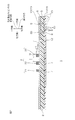
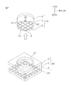
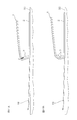
- FIG. 1 shows a plan view of an embodiment of a patch-type biosensor of the present invention.
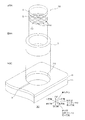
- FIG. 2 is a cross-sectional view taken along the longitudinal direction of the adhesive biosensor shown in FIG. 1, and more specifically, a side cross-sectional view taken along the line AA.
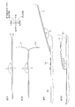
- FIGS. 3A to 3D are side views for explaining a method of applying the skin to the adhesive type biosensor shown in FIGS. 1 and 2 and a state in which stress is applied to the electronic component
- FIG. 3A is an adhesive type biosensor.
- FIG. 3B peels a portion of the first release sheet from the substrate to expose a portion of the substrate
- FIG. 3C pressure sensitively adheres a portion of the substrate to the skin
- FIG. 3D shows a process
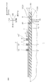
- FIG. 4 shows a side sectional view when the patch-type biosensor shown in FIG. 2 is stuck to the skin.
- 5A to 5D are manufacturing process diagrams of the base in the patch type biosensor shown in FIG. 2, wherein FIG. 5A is a step of preparing a base layer and a wiring layer, and FIG. 5B is a pressure-sensitive adhesive layer and a base A step of bonding material layers, FIG. 5C shows a step of forming an opening, a step of preparing a probe member, a step of FIG. 5D is a step of fitting a probe member into the opening, and a step of forming a connecting portion.
- FIG. 5A is a step of preparing a base layer and a wiring layer
- FIG. 5B is a pressure-sensitive adhesive layer and a base
- FIG. 5C shows a step of forming an opening
- a step of preparing a probe member
- a step of FIG. 5D is a step of fitting a probe member into the opening
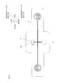
- FIG. 6 is a perspective view of the probe-containing sheet as viewed from below, and shows a perspective view in which a part of the second release sheet is cut away.
- FIG. 7 is a perspective view for explaining the manufacturing process of the probe member, and the upper side view is a perspective view seen from the other side in the thickness direction, and the lower side view is a perspective view seen from one side in the thickness direction.
- 8A to 8C are exploded perspective views of the probe member, and FIG. 8A shows the probe member, FIG. 8B shows the connection portion, and FIG. 8C shows the opening at one end in the longitudinal direction of the substrate.
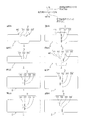
- 9A to 9H show modified examples of the sticking type biosensor.
- FIG. 10 shows a plan view of the patch-type biosensor of Comparative Example 1 in which the longitudinal direction of the electronic component is along the longitudinal direction of the substrate.
- 11A and 11B show side views for explaining a state in which stress is applied to the electronic component along the longitudinal direction of the adhesive biosensor of Comparative Example 1 shown in FIG. 10, and FIG. 11A shows stress in the electronic component. 11B shows that the electronic component is damaged by the stress.
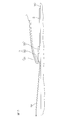
- the longitudinal direction of each of a several electronic component shows the top view of the sticking type
- FIG. 13 is a side view illustrating a state in which adjacent electronic components are in contact with each other along the longitudinal direction of the adhesive biosensor of Comparative Example 2 illustrated in FIG.
- layers or the like included in the electronic component 3 clearly show the side view shape of the electronic component 3. Is omitted.
- the sticking type biosensor 1 has a substantially flat plate shape extending in the longitudinal direction.
- the sticking type biosensor 1 includes a base 2 and an electronic component 3 disposed on one surface of the base 2 in the thickness direction.
- the base material 2 is a base material for attachment with a circuit part, and for example, is a base material having stretchability (flexibility) and pressure-sensitive adhesiveness while having a circuit part 36 (described later).
- the substrate 2 is a flat plate extending in the longitudinal direction, and is a sheet having excellent stretchability.
- the base material 2 has a strip extending in the longitudinal direction, and the longitudinal central portion 46 bulges outward in the lateral direction (direction orthogonal to the longitudinal direction and the thickness direction) (width direction) Have.
- the base 2 includes the pressure-sensitive adhesive layer 5, the base layer 6, the wiring layer 7, the probe 8, and the connection portion 9.
- the pressure-sensitive adhesive layer 5 forms the other surface (pressure-sensitive adhesive surface) in the thickness direction of the substrate 2. That is, the pressure-sensitive adhesive layer 5 is a layer that imparts pressure-sensitive adhesiveness to the other surface of the stick-type biosensor 1 in the thickness direction in order to stick the substrate 2 to the surface of the living body (such as the skin 50 in FIG. 4). It is.
- the pressure sensitive adhesive layer 5 forms the outer shape of the substrate 2.
- the pressure sensitive adhesive layer 5 has a flat plate shape extending in the longitudinal direction.
- the pressure-sensitive adhesive layer 5 has two first openings 11 at both longitudinal ends. Each of the two first openings 11 has a substantially ring shape in plan view. The first opening 11 penetrates the thickness direction of the pressure-sensitive adhesive layer 5. Further, the other surface in the thickness direction on the inner side of the first opening 11 is opened toward the other side in the thickness direction, and has a first groove 10 corresponding to the probe 8.
- the material of the pressure-sensitive adhesive layer 5 is not particularly limited as long as the material has pressure-sensitive adhesion, for example.
- the pressure-sensitive adhesive layer 5 is also an elastic material having elasticity.
- the base layer 6 forms one surface in the thickness direction of the base 2.
- the base layer 6 forms the outer shape (the shape projected in the thickness direction) of the base 2 together with the pressure-sensitive adhesive layer 5.
- the plan view shape of the base material layer 6 is the same as the plan view shape of the pressure sensitive adhesive layer 5.
- the base layer 6 is disposed on the entire surface in the thickness direction of the pressure-sensitive adhesive layer 5.
- the base layer 6 is a support layer that supports the pressure-sensitive adhesive layer 5.
- the base layer 6 has a flat plate shape extending in the longitudinal direction.
- the base material layer 6 has the 2nd groove
- the second groove 12 has the same pattern shape as the wiring layer 7 in plan view. The second groove 12 is opened toward one side in the thickness direction.
- the base layer 6 also has a second opening 13 corresponding to the first opening 11.
- the second opening 13 communicates with the first opening 11 in the thickness direction.
- the second opening 13 has a substantially ring shape in plan view having the same shape and the same size as the first opening 11.
- Examples of the material of the base layer 6 include an insulator having stretchability.
- resin such as polyurethane-type resin, is mentioned, for example.
- the breaking elongation of the base material layer 6 is, for example, 100% or more, preferably 200% or more, more preferably 300% or more, and for example, 2000% or less. If the breaking elongation is at least the above lower limit, the material of the base material layer 6 has excellent stretchability.
- the wiring layer 7 is embedded in, for example, the second groove 12. Specifically, the wiring layer 7 is embedded in one side of the base layer 6 in the thickness direction such that one side in the thickness direction is exposed from the base layer 6. The thickness direction one surface of the wiring layer 7 forms the thickness direction one surface of the base material 2 together with the thickness direction one surface of the base material layer 6 and the electronic component 3.
- the wiring layer 7 has a wiring pattern for connecting the connection portion 9 and the electronic component 3 (described later).
- Wiring layer 7 includes component terminals (not shown) used for electrical connection with electronic component 3.
- the width (line width) of the wiring layer 7 is set in a range that does not inhibit the stretchability of the base layer 6, and is, for example, 2000 ⁇ m or less, preferably 500 ⁇ m or less, or, for example, 50 ⁇ m. The above, preferably, 200 ⁇ m or more.
- Examples of the material of the wiring layer 7 include conductors such as copper, nickel, gold, and their alloys. As a material of the wiring layer 7, preferably, copper is mentioned.
- the probe 8 contacts the skin 50 when the pressure-sensitive adhesive layer 5 is attached to the skin 50 as shown in FIG. 4, and senses the electrical signal from the living body, temperature, vibration, sweat, metabolites, etc. Electrode (bioelectrode).
- the probe 8 is embedded in the pressure sensitive adhesive layer 5 so as to be exposed from the other surface in the thickness direction of the pressure sensitive adhesive layer 5. That is, the probe 8 is embedded in the first groove 10 in the pressure-sensitive adhesive layer 5 inside the first opening 11.
- the probe 8 is disposed on the other surface of the pressure-sensitive adhesive layer 5 forming the first groove 10 in the thickness direction.
- the probe 8 forms the other surface of the base 2 in the thickness direction together with the pressure-sensitive adhesive layer 5.
- the probe 8 has a net shape, preferably a substantially grid shape in plan view (or a substantially mesh shape).
- the outer side surface located in the outermost side among the side surfaces of the probe 8 forms the virtual circle which passes them in planar view.
- the material of the probe 8 include the materials (specifically, conductors) exemplified for the wiring layer 7.
- the outer dimensions of the probe 8 are set such that the virtual circle passing through the outer side surface 22 overlaps the inner peripheral surface defining the first opening 11 in plan view.
- connection portion 9 is provided corresponding to the second opening 13 and the first opening 11 and has the same shape as them.
- the connection portion 9 penetrates (passes) the base material layer 6 and the pressure-sensitive adhesive layer 5 in the thickness direction, and is filled in the second opening 13 and the first opening 11.
- the connection portion 9 has an endless shape in plan view along the outer side surface 22 of the probe 8 as shown in FIG. 8B.
- the connection portion 9 has a substantially cylindrical shape in which an axis extends in the thickness direction (along an imaginary circle passing through the outer side surface 22).
- connection portion 9 is in contact with the outer surface 22 of the probe 8.
- the connection portion 9 is pressure-sensitively adhered to the pressure-sensitive adhesive layer 5 outside the first opening 11 and the pressure-sensitive adhesive layer 5 inside the first opening 11.
- the connecting portion 9 is in contact with the base layer 6 outside the second opening 13 and the base layer 6 inside the second opening 13.
- the thickness direction one surface of the connection portion 9 is flush with the thickness direction one surface of the base material layer 6.
- the other surface in the thickness direction of the connection portion 9 is flush with the other surface in the thickness direction of the pressure-sensitive adhesive layer 5.
- connection portion 9 located on one side in the longitudinal direction is one end of the wiring layer 7 located on one side in the longitudinal direction at one end in the thickness direction. Be continuous.
- the connecting portion 9 located on the other side in the longitudinal direction is continuous with the other end edge in the longitudinal direction of the wiring layer 7 located on the other side in the longitudinal direction at one end in the thickness direction. That is, the connection portion 9 is electrically connected to the wiring layer 7.
- connection portion 9 electrically connects the wiring layer 7 and the probe 8.
- connection part 9 As a material of the connection part 9, a metal, electroconductive resin (including electroconductive polymer), etc. are mentioned, for example, Preferably, electroconductive resin etc. are mentioned.
- connection portion 9 and the wiring layer 7 constitute a circuit portion 36 which electrically connects the probe 8 to the electronic component 3. That is, the circuit portion 36 includes the wiring layer 7 disposed on one surface of the base 2 in the thickness direction, and the connection portion 9 passing the base 2 in the thickness direction. Preferably, the circuit portion 36 is formed only of the wiring layer 7 and the connection portion 9.
- an analog front end for processing and storing as an electric signal from a living body acquired by the probe 8, a microcomputer, a logic IC such as a memory, and further convert the electric signal into a radio wave Transmitter such as a communication IC for wireless transmission to an external receiver, or an interposer.
- a radio wave Transmitter such as a communication IC for wireless transmission to an external receiver, or an interposer.
- one or more may be selected appropriately from the above-described examples.
- the electronic component 3 is disposed at one longitudinal direction central portion 46 of the base 2 in the lateral direction.
- a plurality of (for example, three) electronic components 3 are arranged at intervals in the longitudinal direction of the substrate 2.
- the electronic component 3 includes a first component 31, a second component 32, and a third component 33, which are arranged in order from the other side in the longitudinal direction of the base 2 to one side.
- the first component 31 is an analog front end
- the second component 32 is a memory
- the third component 33 is a communication IC.
- Each of the plurality of electronic components 3 extends in the longitudinal direction LD of the electronic component 3.
- the longitudinal direction LD of the electronic component 3 intersects the short side direction of the base material 2, and specifically, is orthogonal to the short side direction of the base material 2.
- each of the plurality of electronic components 3 has a substantially rectangular shape in plan view extending along a long direction of the base 2.
- the plurality of electronic components 3 overlap when projected in the longitudinal direction.
- one end 37 (longitudinal one end edge) on the side facing the one end edge of the base 2 is the same when projected in the longitudinal direction of the base 2. It is placed in position.
- the electronic component 3 is disposed on one surface of the base 2 in the thickness direction. Specifically, the electronic component 3 is in contact with one surface of the base layer 6 in the thickness direction.
- the electronic component 3 has a substantially rectangular plate shape in cross section.
- a terminal (not shown) is provided on the other surface of the electronic component 3 in the thickness direction. The terminal (not shown) of the electronic component 3 is electrically connected to the component terminal (not shown) of the wiring layer 7.
- the electronic component 3 is harder than, for example, the pressure sensitive adhesive layer 5 and the base material layer 6. Therefore, as a material of the electronic component 3, a hard material is mentioned, for example, For example, a silicon-type inorganic material is mentioned.
- the length L of the longitudinal direction LD of the electronic component 3 is not particularly limited as long as it exceeds the above-mentioned width W.
- the ratio (L / W) of the longitudinal length L to the width W exceeds 1, preferably , 1.2 or more, more preferably, 1.5 or more, and for example, 10 or less.
- the length L of the electronic component 3 means the length of the electronic component 3 in the short direction of the substrate 2.
- the thickness T of the electronic component 3 is, for example, 20 ⁇ m or more, preferably 50 ⁇ m or more, and for example, 3000 ⁇ m or less, preferably 1000 ⁇ m or less.
- the maximum thickness Tmax of the adjacent electronic component 3 is, for example, 20 ⁇ m or more, preferably 50 ⁇ m or more, and for example, 3000 ⁇ m or less, preferably 1000 ⁇ m or less.
- the maximum thickness Tmax means the thickness of the electronic component 3 having a large thickness when two electronic components 3 having different thicknesses are adjacent to each other.
- the spacing I between the adjacent electronic components 3 is, for example, 40 ⁇ m or more, preferably 100 ⁇ m or more, and for example, 6000 ⁇ m or less, preferably 2000 ⁇ m or less.
- the spacing I corresponds to the distance between the adjacent electronic components 3 in the short direction of the substrate 2.
- the ratio (I / Tmax) of the distance I between two adjacent electronic components 3 to the maximum thickness Tmax of the two electronic components 3 is, for example, 2 or more, preferably 2.5 or more, more preferably, It is three or more, for example, four or less.
- the plurality of electronic components 3 can be disposed with high efficiency and space saving.
- the width W of the electronic component 3 is a length in the direction orthogonal to the longitudinal direction LD of the electronic component 3 and corresponds to the length of the electronic component 3 in the longitudinal direction of the base 2, specifically, 5000 ⁇ m or less Preferably, it is 4000 ⁇ m or less, more preferably, 3000 ⁇ m or less, and for example, 1000 ⁇ m or more.
- the width W is equal to or less than the above-described upper limit, when the substrate 2 is attached to the skin 50, damage when the electronic component 3 is stressed can be effectively suppressed.
- the sticking type biometric sensor 1 is provided with the 1st peeling sheet 19 as an example of a peeling sheet.
- the first release sheet 19 forms the lowermost surface of the adhesive type biosensor 1.
- the first release sheet 19 is disposed on the other surface of the base 2 in the thickness direction.
- the first release sheet 19 is a protective sheet that covers the other surface of the base 2 in the thickness direction (the pressure-sensitive adhesive surface of the pressure-sensitive adhesive layer 5) and protects it from scratches, dust, and the like.
- the first peelable sheet 19 is a peelable sheet which is peeled from the base 2 along the longitudinal direction of the base 2 when the attached biosensor 1 is in use (see FIGS. 3B to 3D).
- the first release sheet 19 has, for example, a substantially flat plate shape extending in the longitudinal direction of the substrate 2.
- the material of the first release sheet 19 include resins (polymers) such as polyester (such as polyethylene terephthalate) and polyolefins (such as polypropylene), and metals such as aluminum and stainless steel.
- the material of the first release sheet 19 is preferably a resin from the viewpoint of stretchability.
- a substrate 2 is prepared according to FIGS. 5A-5D.
- the substrate layer 6 and the wiring layer 7 are prepared.
- the base material layer 6 and the wiring layer 7 are prepared such that the wiring layer 7 is embedded in the second groove 12 by the method described in JP-A-2017-22236 and JP-A-2017-22237.
- the pressure-sensitive adhesive layer 5 is disposed on the other surface of the base layer 6 in the thickness direction.
- a coating solution containing the material of the pressure-sensitive adhesive layer 5 is prepared, and then, the coating solution is applied to one surface of the first release sheet 19 in the thickness direction And then dried by heating.
- the pressure sensitive adhesive layer 5 is disposed on one surface of the first release sheet 19 in the thickness direction.
- the pressure-sensitive adhesive layer 5 and the base material layer 6 are attached to each other by, for example, a laminator. Specifically, one surface of the pressure-sensitive adhesive layer 5 in the thickness direction is brought into contact with the other surface of the base layer 6 in the thickness direction.
- each of the base material layer 6 and the pressure-sensitive adhesive layer 5 does not have the second opening 13 and the first opening 11 (opening 23) (see FIG. 5C).
- the openings 23 are formed in the base layer 6 and the pressure-sensitive adhesive layer 5.
- the opening 23 penetrates the base layer 6 and the pressure-sensitive adhesive layer 5.
- the opening 23 is a hole (through hole) having a substantially circular shape in a plan view and divided by an outer peripheral surface that divides the second opening 13 and an outer peripheral surface that divides the first opening 11.
- the opening 23 is opened toward one side in the thickness direction.
- the lower end of the opening 23 is closed by the first release sheet 19.
- the pressure-sensitive adhesive layer 5 and the base material layer 6 are punched and half-etched, for example.
- the probe member 18 is then prepared and fitted into the opening 23.
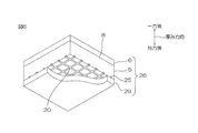
- the probe-containing sheet 26 is prepared.
- the probe-containing sheet 26 is formed on the second release sheet 29, the probe pattern 25 formed on one side in the thickness direction of the second release sheet 29, and on the one side in the thickness direction of the second release sheet 29, A pressure-sensitive adhesive layer 5 to be embedded and a base material layer 6 disposed on one surface in the thickness direction of the pressure-sensitive adhesive layer 5 are provided.
- the second release sheet 29 has the same configuration as the first release sheet 19 described above.
- the probe pattern 25 has the same pattern shape as the probe 8, and the material of the probe pattern 25 is the same as the material of the probe 8.
- the probe pattern 25 has a larger planar area than an imaginary circle passing through the outer surface 22 of the probe 8.
- Each of the pressure-sensitive adhesive layer 5 and the substrate layer 6 in the probe-containing sheet 26 has the same configuration as each of the pressure-sensitive adhesive layer 5 and the substrate layer 6 described above.
- the probe-containing sheet 26 is prepared, for example, by the methods described in JP-A-2017-22236 and JP-A-2017-22237.
- the cutting lines 27 are formed on the probe pattern 25, the pressure-sensitive adhesive layer 5 and the base layer 6 in a substantially circular shape in plan view.
- the cutting line 27 is formed by, for example, punching.
- the cutting line 27 divides the probe pattern 25, the pressure-sensitive adhesive layer 5 and the base layer 6 into and out of the same, but is not formed on the second release sheet 29.
- the dimensions of the cutting line 27 are the same as the inner diameters of the first opening 11 and the second opening 13. That is, the cutting line 27 coincides with an imaginary circle passing through the outer side surface 22.
- the formation of the cutting line 27 forms the probe member 18.
- the outer side surface 22 of the probe 8 is flush with the outer side surface of the pressure sensitive adhesive layer 5. In the probe member 18, the outer side surface 22 is exposed radially outward from the outer side surface of the pressure-sensitive adhesive layer 5.
- the probe member 18 is pulled up from the second release sheet 29. Specifically, the other surface in the thickness direction of the probe member 18 is peeled off from the second peeling sheet 29.
- the probe member 18 is fitted into the opening 23.
- connection portion 9 is provided in the second opening 13 and the first opening 11.
- the conductive resin composition (conductive composition liquid) is injected (or applied) to the second opening 13 and the first opening 11 Do. Thereafter, the conductive resin composition (conductive composition liquid) is heated to remove the solvent, and at the same time, the binder resin is crosslinked by the crosslinking agent.
- the laminated body 30 for biosensors provided with the base material 2 and the 1st peeling sheet 19 is produced.
- the biosensor stack 30 does not include the electronic component 3 (further, the battery 45), that is, it is not an adhesive type biosensor 1 but an intermediate component for manufacturing the adhesive type biosensor 1 .
- the plurality of electronic components 3 are mounted on the biosensor stack 30. Specifically, the terminal (not shown) of electronic component 3 is brought into contact with the component terminal (not shown) in wiring layer 7, and the other surface in the thickness direction of electronic component 3 is made the thickness of base material layer 6 Contact with one side of the direction.
- the sticking type biosensor 1 including the base 2, the electronic component 3 and the first release sheet 19 is manufactured.
- the patch-type biosensor 1 preferably includes only the base 2, the electronic component 3, and the first release sheet 19.
- the battery 45 is mounted on the patch-type biosensor 1 as shown by the phantom line in FIG. 1.
- the battery 45 has a substantially flat (box) shape extending in the surface direction.
- the battery 45 has a terminal (not shown) provided on the other surface in the thickness direction.
- the terminal (not shown) of the battery 45 is electrically connected to the battery terminal (not shown) of the wiring layer 7. At that time, the other surface in the thickness direction of the battery 45 is brought into contact with one surface in the thickness direction of the base material layer 6.
- the first release sheet 19 (see the arrow and the phantom line in FIG. 3D) is removed from the base 2 and the base 2 is attached to the skin 50.
- one longitudinal end edge of the first release sheet 19 (a portion of the first release sheet 19 facing the longitudinal end edge of the base material 2)
- the one longitudinal side portion of the first release sheet 19 is peeled away from the one longitudinal side portion of the substrate 2 while being peeled.
- the longitudinal direction one side portion of the thickness direction other surface (pressure-sensitive adhesive surface) of the base material 2 is exposed toward the other thickness direction side.
- the other surface (pressure-sensitive adhesive surface) in the thickness direction of the substrate 2 is pressure-sensitively adhered to the surface of the skin 50.
- the other longitudinal side portion of the first release sheet 19 is peeled off from the other longitudinal side portion of the substrate 2, and the other longitudinal side portion of the substrate 2 is Is exposed, and immediately thereafter, the portion is pressure-sensitively adhered to the surface of the skin 50.
- the first release sheet 19 is removed from the patch-type biosensor 1, and the other surface (pressure-sensitive adhesive surface) of the base 2 in the thickness direction is adhered to the surface of the skin 50.
- the probe 8 senses as an electrical signal from a living body, and the electrical signal sensed by the probe 8 is input to the electronic component 3 through the connection portion 9 and the wiring layer 7.
- the electronic component 3 processes the electrical signal based on the power supplied from the battery 45 and stores it as information. Furthermore, if necessary, the electric signal is converted into a radio wave, which is wirelessly transmitted to an external receiver.
- the operation of the first component 31, the second component 32, and the third component 33 in the electronic component 3 is as follows. If the sticking type biosensor 1 is a sticking type electrocardiograph (described later), the potential change of the heart acquired by the probe 8 is converted into digital data by the first component 31 which is an analog front end, and the second component which is a memory Record potential changes in the heart at 32. As an example, the potential change of the heart is recorded in the second part 32 at a data rate of 16 bits and 1 kHz. In addition, the third component 33 which is a communication IC wirelessly transmits the signal acquired by the probe 8 to the outside.
- the sticking type biosensor 1 is a sticking type electrocardiograph (described later)
- the potential change of the heart acquired by the probe 8 is converted into digital data by the first component 31 which is an analog front end
- the second component which is a memory Record potential changes in the heart at 32.
- the potential change of the heart is recorded in the second part 32 at a data rate of 16 bits and 1 kHz.
- the patch-type biosensor 1 After the above operation (that is, after sensing of the living body by the patch-type biosensor 1), the patch-type biosensor 1 is removed from the skin 50, and the recorded data is extracted from the second part 32 and analyzed. Thereafter, the second part 32 (and, if necessary, the first part 31 and the third part 33) is reused.
- the longitudinal direction LD of the electronic component 3 is orthogonal to the longitudinal direction of the base 2, the stress applied to the electronic component 3 can be reduced more reliably.
- the adhesive type biosensor 1 since the longitudinal direction LD of the electronic component 3 intersects with the longitudinal direction of the base 2, even when the first release sheet 19 is peeled from the base 2 The stress applied to the electronic component 3 can be reduced. Therefore, when the substrate 2 is attached to the skin 50, damage to the electronic component 3 can be further reliably suppressed.
- the plurality of electronic components 3 having the longitudinal direction LD along the longitudinal direction of the substrate 2 and arranged adjacent to the longitudinal direction of the substrate 2 are the substrate 2 described above as shown in FIGS. 12 and 13.
- the deformation along the longitudinal direction may cause contact with each other and damage due to this (Comparative Example 2). Specifically, damage due to the contact of the first part 31 and the second part 32 or the contact of the second part 32 and the third part 33 is assumed.
- this sticking type biosensor 1 at least one selected from the group consisting of an analog front end, a microcomputer, a memory, an interposer and a chip is hard or brittle, so the electronic component 3 is damaged when stressed. May occur.
- the adhesive type biosensor 1 since the longitudinal direction LD of the electronic component 3 intersects with the longitudinal direction of the base 2, the stress applied to the electronic component 3 can be reduced.
- the electronic component 3 is provided with the first component 31 which is an analog front end, the second component 32 which is a memory, and the third component 33 which is a communication IC, The sensing performance of the sensor 1 can be improved.
- the patch-type biosensor 1 is not particularly limited as long as it is a device capable of monitoring the state of a living body by sensing an electrical signal from the living body, for example.
- a patch-type electrocardiograph, a patch-type electroencephalograph And a patch-type sphygmomanometer, a patch-type pulsimeter, a patch-type electromyograph, a patch-type thermometer, and a patch-type accelerometer may be individual devices or a plurality of devices may be incorporated in one device.
- the patch-type biosensor 1 is preferably used as a patch-type electrocardiograph.
- the probe 8 senses the action potential of the heart as an electrical signal.
- a living body includes living bodies other than a human body and a human body, Preferably, it is a human body.
- the patch-type biosensor 1 may not include the first release sheet 19 and may include the base 2, the electronic component 3 and (only).
- the patch-type biosensor 1 includes a first release sheet 19, a base 2, and an electronic component 3.
- the first release sheet 19 can protect the pressure-sensitive adhesive surface of the substrate 2 from scratches, dust, and the like.
- FIG. 3B when the first release sheet 19 is removed along the longitudinal direction of the substrate 2, the substrate 2 tends to be deformed.
- the stress applied to the electronic component 3 is reduced even when the first release sheet 19 is peeled from the base material 2 be able to.
- the longitudinal direction LD of the electronic component 3 may cross the longitudinal direction of the substrate 2, that is, although not shown, the longitudinal direction LD of the electronic component 3 is orthogonal to the longitudinal direction of the substrate 2 although it does not, it may cross.
- the longitudinal directions LD of the plurality of electronic components 3 are inclined with respect to the longitudinal direction of the substrate 2.
- the angle between the longitudinal direction LD of the electronic component 3 and the longitudinal direction of the base material 2 is, for example, more than 0 degrees, and further 30 degrees or more, and for example, less than 90 degrees and less than 60 degrees.
- the longitudinal direction LD crossing (orthogonal to) the longitudinal direction of the substrate 2 may be provided with the electronic component 3, for example, one of the plurality of electronic components 3 with respect to the longitudinal direction of the substrate 2
- the other may have a longitudinal direction LD along the longitudinal direction of the substrate 2.
- the longitudinal direction LD of one or more of the electronic components 3 intersects (orthogonalizes) the longitudinal direction of the base material 2, preferably more than half of the electronic components 3.
- the longitudinal direction LD of the component 3 intersects (orthogonal to) the longitudinal direction of the substrate 2, and more preferably, the longitudinal direction LD of the electronic component 3 of 80% or more intersects the longitudinal direction of the substrate 2 More preferably, the longitudinal directions LD of all the electronic components 3 intersect (orthogonal) the longitudinal direction of the substrate 2.
- the arrangement of the plurality of electronic components 3 is not limited to the above, and examples thereof include the arrangements shown in FIGS. 9B to 9H.
- the plurality of electronic components 3 are spaced apart in the lateral direction of the substrate 2 It is done.
- the plurality of electronic components 3 are disposed at the center of the base 2 in the short direction.
- Each of the short direction end edges of the substrate 2 extends in a straight line along the longitudinal direction of the substrate 2 across the longitudinal central portion 46 and the longitudinal ends.
- the plurality of electronic components 3 are arranged spaced apart from each other in both the longitudinal direction and the lateral direction of the substrate 2.
- the electronic component 3 includes the first component 31, the second component 32 and the third component 33, and the second component 32 which are disposed apart from each other in the longitudinal direction.
- the fourth part 34 and the fifth part 35 are disposed at intervals on both sides in the short direction.
- the first part 31 and the second part 32 are disposed at an interval in the longitudinal direction of the base 2, and the third part 33 and the fourth part 34 are also of the base 2. It is spaced apart in the longitudinal direction.
- Each of the third component 33 and the fourth component 34 is disposed opposite to the first component 31 and the second component 32 at an interval on the other side in the short direction.
- the plurality of electronic components 3 are arranged offset from one another.
- the first part 31 and the third part 33 are shifted with the second part 32 and the fourth part 34 when projected in the longitudinal direction of the base material 2 and do not overlap.
- one side of the base 2 is short.
- they are arranged in order from the other side to the one side in the longitudinal direction of the base material 2.
- FIGS. 9A to 9H those are preferably the modifications shown in FIGS. 9B, 9D, 9F, 9G, and 9H, and more preferably the modifications shown in FIGS. 9B, 9F, and 9H. is there.
- the patch-type biosensor is used, for example, in a patch-type electrocardiograph, a patch-type electroencephalograph, a patch-type sphygmomanometer, a patch-type pulsimeter, a patch-type electromyograph, a patch-type thermometer, a patch-type accelerometer, and the like.
Abstract
L'invention concerne un biocapteur de type à adhérence, comprenant : un substrat pour adhérer à une surface d'un organisme, le substrat s'étendant dans une direction longitudinale et ayant des propriétés élastiques ; et un composant électronique disposé sur une surface du substrat dans la direction de l'épaisseur de celui-ci et s'étendant dans la direction longitudinale. La direction longitudinale du composant électronique croise la direction longitudinale du substrat.
Priority Applications (4)
| Application Number | Priority Date | Filing Date | Title |
|---|---|---|---|
| EP18876597.8A EP3708074A4 (fr) | 2017-11-10 | 2018-10-25 | Biocapteur de type à adhérence |
| US16/762,319 US11510623B2 (en) | 2017-11-10 | 2018-10-25 | Patchable biosensor |
| JP2019552709A JP7222905B2 (ja) | 2017-11-10 | 2018-10-25 | 貼付型生体センサ |
| CN201880072568.0A CN111315288B (zh) | 2017-11-10 | 2018-10-25 | 贴附型生物传感器 |
Applications Claiming Priority (2)
| Application Number | Priority Date | Filing Date | Title |
|---|---|---|---|
| JP2017217040 | 2017-11-10 | ||
| JP2017-217040 | 2017-11-10 |
Publications (1)
| Publication Number | Publication Date |
|---|---|
| WO2019093144A1 true WO2019093144A1 (fr) | 2019-05-16 |
Family
ID=66439218
Family Applications (1)
| Application Number | Title | Priority Date | Filing Date |
|---|---|---|---|
| PCT/JP2018/039750 WO2019093144A1 (fr) | 2017-11-10 | 2018-10-25 | Biocapteur de type à adhérence |
Country Status (5)
| Country | Link |
|---|---|
| US (1) | US11510623B2 (fr) |
| EP (1) | EP3708074A4 (fr) |
| JP (1) | JP7222905B2 (fr) |
| CN (1) | CN111315288B (fr) |
| WO (1) | WO2019093144A1 (fr) |
Cited By (2)
| Publication number | Priority date | Publication date | Assignee | Title |
|---|---|---|---|---|
| JPWO2021152919A1 (fr) * | 2020-01-30 | 2021-08-05 | ||
| EP3906964A1 (fr) * | 2020-05-08 | 2021-11-10 | Heraeus Deutschland GmbH & Co KG | Électrodes encastrées pour substrats souples |
Citations (8)
| Publication number | Priority date | Publication date | Assignee | Title |
|---|---|---|---|---|
| JPH06245915A (ja) * | 1993-02-23 | 1994-09-06 | Tsutomu Otake | 生体電気信号記録具 |
| JP2002541893A (ja) * | 1999-04-15 | 2002-12-10 | ネキサン・リミテツド | 携帯型遠隔式患者テレモニタリングシステム |
| US20060030781A1 (en) * | 2004-08-05 | 2006-02-09 | Adnan Shennib | Emergency heart sensor patch |
| US20070191728A1 (en) * | 2006-02-10 | 2007-08-16 | Adnan Shennib | Intrapartum monitor patch |
| JP2012010978A (ja) | 2010-06-30 | 2012-01-19 | Japan Science & Technology Agency | 生体適合性ポリマー基板 |
| JP2017022236A (ja) | 2015-07-09 | 2017-01-26 | 日東電工株式会社 | 配線回路基板の製造方法 |
| JP2017022237A (ja) | 2015-07-09 | 2017-01-26 | 日東電工株式会社 | 配線回路基板 |
| JP2018164725A (ja) * | 2017-03-28 | 2018-10-25 | 国立大学法人大阪大学 | 生体信号測定装置及びプログラム |
Family Cites Families (38)
| Publication number | Priority date | Publication date | Assignee | Title |
|---|---|---|---|---|
| JPH05159994A (ja) * | 1991-12-09 | 1993-06-25 | Takeshi Ikeda | 電子部品の製法 |
| JP2003330041A (ja) * | 2002-05-10 | 2003-11-19 | Sharp Corp | 半導体装置及びそれを備えた表示パネルモジュール |
| DE10354833A1 (de) | 2003-11-24 | 2005-06-23 | Liedtke, Rainer K., Dr. | Dermale diagnostische Pflastersysteme mit aktiven Transpondern |
| JP2005236137A (ja) * | 2004-02-20 | 2005-09-02 | Fujikura Ltd | 封止剤、メンブレン回路基板 |
| JP2006137184A (ja) * | 2004-10-13 | 2006-06-01 | Furukawa Electric Co Ltd:The | 電気電子部品用金属材料及びその製造方法 |
| JP2006131331A (ja) * | 2004-11-05 | 2006-05-25 | Brother Ind Ltd | タグテープロール及び無線タグ回路素子カートリッジ |
| AU2006222414B2 (en) * | 2005-03-09 | 2011-03-03 | Delta Dansk Elektronik, Lys Og Akustik | A three-dimensional adhesive device having a microelectronic system embedded therein |
| WO2007038607A2 (fr) * | 2005-09-27 | 2007-04-05 | Telzuit Technologies, Llc | Appareil et procede de surveillance de patients |
| JP2007180197A (ja) | 2005-12-27 | 2007-07-12 | Sanyo Electric Co Ltd | 回路装置 |
| US8244335B2 (en) | 2006-02-06 | 2012-08-14 | The Board Of Trustees Of The Leland Stanford Junior University | Non-invasive cardiac monitor and methods of using continuously recorded cardiac data |
| US20080091090A1 (en) * | 2006-10-12 | 2008-04-17 | Kenneth Shane Guillory | Self-contained surface physiological monitor with adhesive attachment |
| US20090076397A1 (en) * | 2007-09-14 | 2009-03-19 | Corventis, Inc. | Adherent Emergency Patient Monitor |
| US20090076341A1 (en) * | 2007-09-14 | 2009-03-19 | Corventis, Inc. | Adherent Athletic Monitor |
| JP2010039234A (ja) * | 2008-08-06 | 2010-02-18 | Konica Minolta Business Technologies Inc | 画像形成装置に用いられるブラシローラ及びその製造方法 |
| US20130123594A1 (en) * | 2010-03-09 | 2013-05-16 | Arkray, Inc. | Electrochemical Sensor |
| KR101048662B1 (ko) * | 2010-05-03 | 2011-07-14 | 한국과학기술원 | 신체 부착형 센서 및 모니터링 장치 |
| JP2013155241A (ja) * | 2012-01-27 | 2013-08-15 | Nitto Denko Corp | シート状伸長性有機基材 |
| JP5899641B2 (ja) * | 2011-03-31 | 2016-04-06 | 大日本印刷株式会社 | バイオセンサカートリッジ、測定装置及び測定方法 |
| WO2013056126A2 (fr) * | 2011-10-13 | 2013-04-18 | Innovamedix, Inc | Dispositif de surveillance de choc traumatique jetable sans fil |
| JP6294353B2 (ja) | 2013-01-23 | 2018-03-14 | エーブリー デニソン コーポレイション | ワイヤレスセンサパッチとその製造方法 |
| US10244986B2 (en) | 2013-01-23 | 2019-04-02 | Avery Dennison Corporation | Wireless sensor patches and methods of manufacturing |
| KR102096562B1 (ko) | 2013-08-06 | 2020-04-03 | 삼성디스플레이 주식회사 | 회로기판 및 이를 구비한 표시장치 |
| JP2015093167A (ja) * | 2013-11-14 | 2015-05-18 | 日東電工株式会社 | 生体センサ |
| CN104648816A (zh) * | 2013-11-18 | 2015-05-27 | 罗姆股份有限公司 | 电子部件包装体 |
| EP3114911B1 (fr) * | 2014-03-04 | 2023-05-03 | Medidata Solutions, Inc. | Boîtier d'encapsulation souple en plusieurs parties pour dispositifs électroniques |
| CN204246122U (zh) | 2014-04-30 | 2015-04-08 | 苏州博思长健电子科技有限公司 | 穿戴式心电检测装置 |
| EP3171768B1 (fr) * | 2014-08-01 | 2020-09-16 | LifeLens Technologies, LLC | Systèmes de surveillance physiologique modulaire |
| WO2016080082A1 (fr) * | 2014-11-17 | 2016-05-26 | 積水化成品工業株式会社 | Pastille pour électrodes |
| US9378450B1 (en) | 2014-12-05 | 2016-06-28 | Vivalnk, Inc | Stretchable electronic patch having a circuit layer undulating in the thickness direction |
| JP6488189B2 (ja) * | 2015-05-18 | 2019-03-20 | 日本メクトロン株式会社 | 伸縮性配線基板 |
| JP2017113088A (ja) * | 2015-12-21 | 2017-06-29 | パナソニックIpマネジメント株式会社 | 生体センサー・デバイス |
| JP2017132874A (ja) * | 2016-01-27 | 2017-08-03 | リンテック株式会社 | 電子部品貼付用アースラベル |
| JP6982959B2 (ja) * | 2016-02-05 | 2021-12-17 | 日本メクトロン株式会社 | 伸縮基板モジュール、伸縮性配線基板及びそれらの製造方法 |
| US10277386B2 (en) * | 2016-02-22 | 2019-04-30 | Mc10, Inc. | System, devices, and method for on-body data and power transmission |
| US11026598B2 (en) | 2016-02-24 | 2021-06-08 | Bainisha Cvba | Elastic movement sensors and calibration |
| WO2017173462A1 (fr) * | 2016-04-01 | 2017-10-05 | The Regents Of The University Of California | Moniteur de santé multimodal flexible de l'épiderme |
| JP6710091B2 (ja) * | 2016-04-13 | 2020-06-17 | 花王株式会社 | センサー付き着用物品 |
| CN207286046U (zh) | 2017-02-22 | 2018-05-01 | 深圳市岩尚科技有限公司 | 一次性自粘贴片及信号采集设备 |
-
2018
- 2018-10-25 WO PCT/JP2018/039750 patent/WO2019093144A1/fr unknown
- 2018-10-25 EP EP18876597.8A patent/EP3708074A4/fr active Pending
- 2018-10-25 CN CN201880072568.0A patent/CN111315288B/zh active Active
- 2018-10-25 US US16/762,319 patent/US11510623B2/en active Active
- 2018-10-25 JP JP2019552709A patent/JP7222905B2/ja active Active
Patent Citations (8)
| Publication number | Priority date | Publication date | Assignee | Title |
|---|---|---|---|---|
| JPH06245915A (ja) * | 1993-02-23 | 1994-09-06 | Tsutomu Otake | 生体電気信号記録具 |
| JP2002541893A (ja) * | 1999-04-15 | 2002-12-10 | ネキサン・リミテツド | 携帯型遠隔式患者テレモニタリングシステム |
| US20060030781A1 (en) * | 2004-08-05 | 2006-02-09 | Adnan Shennib | Emergency heart sensor patch |
| US20070191728A1 (en) * | 2006-02-10 | 2007-08-16 | Adnan Shennib | Intrapartum monitor patch |
| JP2012010978A (ja) | 2010-06-30 | 2012-01-19 | Japan Science & Technology Agency | 生体適合性ポリマー基板 |
| JP2017022236A (ja) | 2015-07-09 | 2017-01-26 | 日東電工株式会社 | 配線回路基板の製造方法 |
| JP2017022237A (ja) | 2015-07-09 | 2017-01-26 | 日東電工株式会社 | 配線回路基板 |
| JP2018164725A (ja) * | 2017-03-28 | 2018-10-25 | 国立大学法人大阪大学 | 生体信号測定装置及びプログラム |
Non-Patent Citations (1)
| Title |
|---|
| See also references of EP3708074A4 |
Cited By (4)
| Publication number | Priority date | Publication date | Assignee | Title |
|---|---|---|---|---|
| JPWO2021152919A1 (fr) * | 2020-01-30 | 2021-08-05 | ||
| WO2021152919A1 (fr) * | 2020-01-30 | 2021-08-05 | 株式会社村田製作所 | Enveloppe de capteur |
| JP7168107B2 (ja) | 2020-01-30 | 2022-11-09 | 株式会社村田製作所 | センサカバー |
| EP3906964A1 (fr) * | 2020-05-08 | 2021-11-10 | Heraeus Deutschland GmbH & Co KG | Électrodes encastrées pour substrats souples |
Also Published As
| Publication number | Publication date |
|---|---|
| US11510623B2 (en) | 2022-11-29 |
| EP3708074A1 (fr) | 2020-09-16 |
| CN111315288B (zh) | 2024-04-23 |
| JP7222905B2 (ja) | 2023-02-15 |
| CN111315288A (zh) | 2020-06-19 |
| EP3708074A4 (fr) | 2021-07-28 |
| TW201922167A (zh) | 2019-06-16 |
| JPWO2019093144A1 (ja) | 2020-11-12 |
| US20200289058A1 (en) | 2020-09-17 |
Similar Documents
| Publication | Publication Date | Title |
|---|---|---|
| CN110573070B (zh) | 生物传感器用片材 | |
| JP7450659B2 (ja) | 導電性組成物および生体センサ | |
| JP7033469B2 (ja) | 生体センサ | |
| WO2019093144A1 (fr) | Biocapteur de type à adhérence | |
| JP7017426B2 (ja) | 生体センサ用積層体および生体センサ用積層体の製造方法 | |
| WO2018198571A1 (fr) | Stratifié pour biocapteur et procédé de production de stratifié pour biocapteur | |
| JP5888799B2 (ja) | 生体用電極パッド | |
| JP7037285B2 (ja) | 生体センサ用積層体および生体センサ | |
| TWI835757B (zh) | 貼附型生物體感測器 | |
| WO2019092919A1 (fr) | Capteur biologique à fixation adhésive | |
| CN110545718B (zh) | 生物传感器 |
Legal Events
| Date | Code | Title | Description |
|---|---|---|---|
| 121 | Ep: the epo has been informed by wipo that ep was designated in this application |
Ref document number: 18876597 Country of ref document: EP Kind code of ref document: A1 |
|
| ENP | Entry into the national phase |
Ref document number: 2019552709 Country of ref document: JP Kind code of ref document: A |
|
| NENP | Non-entry into the national phase |
Ref country code: DE |
|
| ENP | Entry into the national phase |
Ref document number: 2018876597 Country of ref document: EP Effective date: 20200610 |