WO2019093144A1 - Adhering-type biosensor - Google Patents
Adhering-type biosensor Download PDFInfo
- Publication number
- WO2019093144A1 WO2019093144A1 PCT/JP2018/039750 JP2018039750W WO2019093144A1 WO 2019093144 A1 WO2019093144 A1 WO 2019093144A1 JP 2018039750 W JP2018039750 W JP 2018039750W WO 2019093144 A1 WO2019093144 A1 WO 2019093144A1
- Authority
- WO
- WIPO (PCT)
- Prior art keywords
- longitudinal direction
- electronic component
- substrate
- base
- layer
- Prior art date
Links
Images


Classifications
-
- A—HUMAN NECESSITIES
- A61—MEDICAL OR VETERINARY SCIENCE; HYGIENE
- A61B—DIAGNOSIS; SURGERY; IDENTIFICATION
- A61B5/00—Measuring for diagnostic purposes; Identification of persons
- A61B5/68—Arrangements of detecting, measuring or recording means, e.g. sensors, in relation to patient
- A61B5/6801—Arrangements of detecting, measuring or recording means, e.g. sensors, in relation to patient specially adapted to be attached to or worn on the body surface
- A61B5/683—Means for maintaining contact with the body
- A61B5/6832—Means for maintaining contact with the body using adhesives
- A61B5/6833—Adhesive patches
-
- A—HUMAN NECESSITIES
- A61—MEDICAL OR VETERINARY SCIENCE; HYGIENE
- A61B—DIAGNOSIS; SURGERY; IDENTIFICATION
- A61B5/00—Measuring for diagnostic purposes; Identification of persons
- A61B5/24—Detecting, measuring or recording bioelectric or biomagnetic signals of the body or parts thereof
- A61B5/25—Bioelectric electrodes therefor
- A61B5/279—Bioelectric electrodes therefor specially adapted for particular uses
- A61B5/28—Bioelectric electrodes therefor specially adapted for particular uses for electrocardiography [ECG]
- A61B5/282—Holders for multiple electrodes
-
- A—HUMAN NECESSITIES
- A61—MEDICAL OR VETERINARY SCIENCE; HYGIENE
- A61B—DIAGNOSIS; SURGERY; IDENTIFICATION
- A61B5/00—Measuring for diagnostic purposes; Identification of persons
- A61B5/68—Arrangements of detecting, measuring or recording means, e.g. sensors, in relation to patient
- A61B5/6801—Arrangements of detecting, measuring or recording means, e.g. sensors, in relation to patient specially adapted to be attached to or worn on the body surface
- A61B5/683—Means for maintaining contact with the body
- A61B5/6832—Means for maintaining contact with the body using adhesives
- A61B5/68335—Means for maintaining contact with the body using adhesives including release sheets or liners
-
- A—HUMAN NECESSITIES
- A61—MEDICAL OR VETERINARY SCIENCE; HYGIENE
- A61B—DIAGNOSIS; SURGERY; IDENTIFICATION
- A61B2562/00—Details of sensors; Constructional details of sensor housings or probes; Accessories for sensors
- A61B2562/02—Details of sensors specially adapted for in-vivo measurements
- A61B2562/0219—Inertial sensors, e.g. accelerometers, gyroscopes, tilt switches
-
- A—HUMAN NECESSITIES
- A61—MEDICAL OR VETERINARY SCIENCE; HYGIENE
- A61B—DIAGNOSIS; SURGERY; IDENTIFICATION
- A61B2562/00—Details of sensors; Constructional details of sensor housings or probes; Accessories for sensors
- A61B2562/12—Manufacturing methods specially adapted for producing sensors for in-vivo measurements
- A61B2562/125—Manufacturing methods specially adapted for producing sensors for in-vivo measurements characterised by the manufacture of electrodes
-
- A—HUMAN NECESSITIES
- A61—MEDICAL OR VETERINARY SCIENCE; HYGIENE
- A61B—DIAGNOSIS; SURGERY; IDENTIFICATION
- A61B2562/00—Details of sensors; Constructional details of sensor housings or probes; Accessories for sensors
- A61B2562/16—Details of sensor housings or probes; Details of structural supports for sensors
- A61B2562/164—Details of sensor housings or probes; Details of structural supports for sensors the sensor is mounted in or on a conformable substrate or carrier
-
- A—HUMAN NECESSITIES
- A61—MEDICAL OR VETERINARY SCIENCE; HYGIENE
- A61B—DIAGNOSIS; SURGERY; IDENTIFICATION
- A61B2562/00—Details of sensors; Constructional details of sensor housings or probes; Accessories for sensors
- A61B2562/18—Shielding or protection of sensors from environmental influences, e.g. protection from mechanical damage
- A61B2562/187—Strain relief means
-
- A—HUMAN NECESSITIES
- A61—MEDICAL OR VETERINARY SCIENCE; HYGIENE
- A61B—DIAGNOSIS; SURGERY; IDENTIFICATION
- A61B5/00—Measuring for diagnostic purposes; Identification of persons
- A61B5/01—Measuring temperature of body parts ; Diagnostic temperature sensing, e.g. for malignant or inflamed tissue
-
- A—HUMAN NECESSITIES
- A61—MEDICAL OR VETERINARY SCIENCE; HYGIENE
- A61B—DIAGNOSIS; SURGERY; IDENTIFICATION
- A61B5/00—Measuring for diagnostic purposes; Identification of persons
- A61B5/02—Detecting, measuring or recording pulse, heart rate, blood pressure or blood flow; Combined pulse/heart-rate/blood pressure determination; Evaluating a cardiovascular condition not otherwise provided for, e.g. using combinations of techniques provided for in this group with electrocardiography or electroauscultation; Heart catheters for measuring blood pressure
- A61B5/0205—Simultaneously evaluating both cardiovascular conditions and different types of body conditions, e.g. heart and respiratory condition
- A61B5/02055—Simultaneously evaluating both cardiovascular condition and temperature
-
- A—HUMAN NECESSITIES
- A61—MEDICAL OR VETERINARY SCIENCE; HYGIENE
- A61B—DIAGNOSIS; SURGERY; IDENTIFICATION
- A61B5/00—Measuring for diagnostic purposes; Identification of persons
- A61B5/02—Detecting, measuring or recording pulse, heart rate, blood pressure or blood flow; Combined pulse/heart-rate/blood pressure determination; Evaluating a cardiovascular condition not otherwise provided for, e.g. using combinations of techniques provided for in this group with electrocardiography or electroauscultation; Heart catheters for measuring blood pressure
- A61B5/021—Measuring pressure in heart or blood vessels
-
- A—HUMAN NECESSITIES
- A61—MEDICAL OR VETERINARY SCIENCE; HYGIENE
- A61B—DIAGNOSIS; SURGERY; IDENTIFICATION
- A61B5/00—Measuring for diagnostic purposes; Identification of persons
- A61B5/02—Detecting, measuring or recording pulse, heart rate, blood pressure or blood flow; Combined pulse/heart-rate/blood pressure determination; Evaluating a cardiovascular condition not otherwise provided for, e.g. using combinations of techniques provided for in this group with electrocardiography or electroauscultation; Heart catheters for measuring blood pressure
- A61B5/024—Detecting, measuring or recording pulse rate or heart rate
- A61B5/02438—Detecting, measuring or recording pulse rate or heart rate with portable devices, e.g. worn by the patient
-
- A—HUMAN NECESSITIES
- A61—MEDICAL OR VETERINARY SCIENCE; HYGIENE
- A61B—DIAGNOSIS; SURGERY; IDENTIFICATION
- A61B5/00—Measuring for diagnostic purposes; Identification of persons
- A61B5/24—Detecting, measuring or recording bioelectric or biomagnetic signals of the body or parts thereof
- A61B5/25—Bioelectric electrodes therefor
- A61B5/251—Means for maintaining electrode contact with the body
- A61B5/257—Means for maintaining electrode contact with the body using adhesive means, e.g. adhesive pads or tapes
- A61B5/259—Means for maintaining electrode contact with the body using adhesive means, e.g. adhesive pads or tapes using conductive adhesive means, e.g. gels
-
- A—HUMAN NECESSITIES
- A61—MEDICAL OR VETERINARY SCIENCE; HYGIENE
- A61B—DIAGNOSIS; SURGERY; IDENTIFICATION
- A61B5/00—Measuring for diagnostic purposes; Identification of persons
- A61B5/24—Detecting, measuring or recording bioelectric or biomagnetic signals of the body or parts thereof
- A61B5/25—Bioelectric electrodes therefor
- A61B5/279—Bioelectric electrodes therefor specially adapted for particular uses
- A61B5/291—Bioelectric electrodes therefor specially adapted for particular uses for electroencephalography [EEG]
-
- A—HUMAN NECESSITIES
- A61—MEDICAL OR VETERINARY SCIENCE; HYGIENE
- A61B—DIAGNOSIS; SURGERY; IDENTIFICATION
- A61B5/00—Measuring for diagnostic purposes; Identification of persons
- A61B5/24—Detecting, measuring or recording bioelectric or biomagnetic signals of the body or parts thereof
- A61B5/25—Bioelectric electrodes therefor
- A61B5/279—Bioelectric electrodes therefor specially adapted for particular uses
- A61B5/296—Bioelectric electrodes therefor specially adapted for particular uses for electromyography [EMG]
Definitions
- the present invention relates to a patch-type biosensor.
- a biocompatible polymer substrate which comprises a longitudinally extending flexible layer and a data acquisition module fixed on one side thereof (see, for example, Patent Document 1).
- the data acquisition module extends in the same direction as the longitudinal direction of the polymer layer. Therefore, when the biocompatible polymer substrate of Patent Document 1 is applied to human skin along the longitudinal direction of the polymer layer, bending (or bending) or the like along the longitudinal direction in the flexible polymer layer Results in At that time, due to the deformation of the polymer layer, a large stress is applied to the data acquisition module, and there is a problem that the data acquisition module is damaged.
- the present invention provides a patch-type biosensor capable of suppressing damage to an electronic component when the substrate is affixed to the surface of a living body.
- the present invention (1) comprises a base material extending in the longitudinal direction and having stretchability and being attached to the surface of a living body, and an electronic component disposed on one surface in the thickness direction of the base material and extending in the longitudinal direction. And a patch-type biosensor, wherein the longitudinal direction of the electronic component intersects with the longitudinal direction of the substrate.
- the longitudinal direction of the electronic component is the longitudinal direction of the substrate And the stress applied to the electronic component can be reduced. Therefore, when the substrate is attached to the surface of the living body, damage to the electronic component can be suppressed.
- the present invention (2) includes the adhesive biosensor as described in (1), in which the longitudinal direction of the electronic component is orthogonal to the longitudinal direction of the substrate.
- the longitudinal direction of the electronic component is the longitudinal direction of the substrate And the stress applied to the electronic component can be further reliably reduced. Therefore, when the substrate is attached to the surface of the living body, damage to the electronic component can be more reliably suppressed.
- the present invention (3) is the patch type according to (1) or (2), further comprising a release sheet which is disposed on the other surface in the thickness direction of the substrate and which is peeled along the longitudinal direction of the substrate Includes a biometric sensor.
- the electronic component includes at least two of the electronic components disposed adjacent to each other along the longitudinal direction of the substrate, according to any one of (1) to (3) Type biometric sensor.
- At least two electronic components arranged adjacent to each other may be damaged by contact with each other due to the deformation along the longitudinal direction of the above-mentioned substrate.
- the ratio (I / Tmax) of the distance I between the two electronic components in the longitudinal direction of the substrate to the maximum thickness Tmax of the electronic components is 2 or more.
- a patch-type biosensor as described in the above.
- the ratio I / Tmax of the distance I between two electronic components in the longitudinal direction of the substrate to the maximum thickness Tmax of the electronic component is 2 or more, the two electronic components are effectively inhibited from contacting each other Thus, damage to the electronic component can be effectively suppressed.
- the present invention (6) is any one of (1) to (5), wherein the electronic component is at least one selected from the group consisting of an analog front end, a microcomputer, a memory, an interposer and a chip. It includes the attached type biosensor as described.
- At least one selected from the group consisting of an analog front end, a microcomputer, a memory, an interposer and a chip is hard or brittle, so the electronic component is damaged when it is stressed There is a case.
- the electronic component is at least one selected from the group consisting of an analog front end, a microcomputer, a memory, an interposer and a chip, its operation can improve the sensing performance of the patch-type biosensor.
- the patch-type biosensor can suppress damage to the electronic component when the substrate is stuck to the surface of the living body.
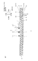
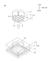
- FIG. 1 shows a plan view of an embodiment of a patch-type biosensor of the present invention.
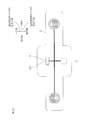
- FIG. 2 is a cross-sectional view taken along the longitudinal direction of the adhesive biosensor shown in FIG. 1, and more specifically, a side cross-sectional view taken along the line AA.
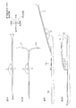
- FIGS. 3A to 3D are side views for explaining a method of applying the skin to the adhesive type biosensor shown in FIGS. 1 and 2 and a state in which stress is applied to the electronic component
- FIG. 3A is an adhesive type biosensor.
- FIG. 3B peels a portion of the first release sheet from the substrate to expose a portion of the substrate
- FIG. 3C pressure sensitively adheres a portion of the substrate to the skin
- FIG. 3D shows a process
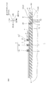
- FIG. 4 shows a side sectional view when the patch-type biosensor shown in FIG. 2 is stuck to the skin.
- 5A to 5D are manufacturing process diagrams of the base in the patch type biosensor shown in FIG. 2, wherein FIG. 5A is a step of preparing a base layer and a wiring layer, and FIG. 5B is a pressure-sensitive adhesive layer and a base A step of bonding material layers, FIG. 5C shows a step of forming an opening, a step of preparing a probe member, a step of FIG. 5D is a step of fitting a probe member into the opening, and a step of forming a connecting portion.
- FIG. 5A is a step of preparing a base layer and a wiring layer
- FIG. 5B is a pressure-sensitive adhesive layer and a base
- FIG. 5C shows a step of forming an opening
- a step of preparing a probe member
- a step of FIG. 5D is a step of fitting a probe member into the opening
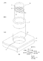
- FIG. 6 is a perspective view of the probe-containing sheet as viewed from below, and shows a perspective view in which a part of the second release sheet is cut away.
- FIG. 7 is a perspective view for explaining the manufacturing process of the probe member, and the upper side view is a perspective view seen from the other side in the thickness direction, and the lower side view is a perspective view seen from one side in the thickness direction.
- 8A to 8C are exploded perspective views of the probe member, and FIG. 8A shows the probe member, FIG. 8B shows the connection portion, and FIG. 8C shows the opening at one end in the longitudinal direction of the substrate.
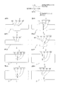
- 9A to 9H show modified examples of the sticking type biosensor.
- FIG. 10 shows a plan view of the patch-type biosensor of Comparative Example 1 in which the longitudinal direction of the electronic component is along the longitudinal direction of the substrate.
- 11A and 11B show side views for explaining a state in which stress is applied to the electronic component along the longitudinal direction of the adhesive biosensor of Comparative Example 1 shown in FIG. 10, and FIG. 11A shows stress in the electronic component. 11B shows that the electronic component is damaged by the stress.
- the longitudinal direction of each of a several electronic component shows the top view of the sticking type
- FIG. 13 is a side view illustrating a state in which adjacent electronic components are in contact with each other along the longitudinal direction of the adhesive biosensor of Comparative Example 2 illustrated in FIG.
- layers or the like included in the electronic component 3 clearly show the side view shape of the electronic component 3. Is omitted.
- the sticking type biosensor 1 has a substantially flat plate shape extending in the longitudinal direction.
- the sticking type biosensor 1 includes a base 2 and an electronic component 3 disposed on one surface of the base 2 in the thickness direction.
- the base material 2 is a base material for attachment with a circuit part, and for example, is a base material having stretchability (flexibility) and pressure-sensitive adhesiveness while having a circuit part 36 (described later).
- the substrate 2 is a flat plate extending in the longitudinal direction, and is a sheet having excellent stretchability.
- the base material 2 has a strip extending in the longitudinal direction, and the longitudinal central portion 46 bulges outward in the lateral direction (direction orthogonal to the longitudinal direction and the thickness direction) (width direction) Have.
- the base 2 includes the pressure-sensitive adhesive layer 5, the base layer 6, the wiring layer 7, the probe 8, and the connection portion 9.
- the pressure-sensitive adhesive layer 5 forms the other surface (pressure-sensitive adhesive surface) in the thickness direction of the substrate 2. That is, the pressure-sensitive adhesive layer 5 is a layer that imparts pressure-sensitive adhesiveness to the other surface of the stick-type biosensor 1 in the thickness direction in order to stick the substrate 2 to the surface of the living body (such as the skin 50 in FIG. 4). It is.
- the pressure sensitive adhesive layer 5 forms the outer shape of the substrate 2.
- the pressure sensitive adhesive layer 5 has a flat plate shape extending in the longitudinal direction.
- the pressure-sensitive adhesive layer 5 has two first openings 11 at both longitudinal ends. Each of the two first openings 11 has a substantially ring shape in plan view. The first opening 11 penetrates the thickness direction of the pressure-sensitive adhesive layer 5. Further, the other surface in the thickness direction on the inner side of the first opening 11 is opened toward the other side in the thickness direction, and has a first groove 10 corresponding to the probe 8.
- the material of the pressure-sensitive adhesive layer 5 is not particularly limited as long as the material has pressure-sensitive adhesion, for example.
- the pressure-sensitive adhesive layer 5 is also an elastic material having elasticity.
- the base layer 6 forms one surface in the thickness direction of the base 2.
- the base layer 6 forms the outer shape (the shape projected in the thickness direction) of the base 2 together with the pressure-sensitive adhesive layer 5.
- the plan view shape of the base material layer 6 is the same as the plan view shape of the pressure sensitive adhesive layer 5.
- the base layer 6 is disposed on the entire surface in the thickness direction of the pressure-sensitive adhesive layer 5.
- the base layer 6 is a support layer that supports the pressure-sensitive adhesive layer 5.
- the base layer 6 has a flat plate shape extending in the longitudinal direction.
- the base material layer 6 has the 2nd groove
- the second groove 12 has the same pattern shape as the wiring layer 7 in plan view. The second groove 12 is opened toward one side in the thickness direction.
- the base layer 6 also has a second opening 13 corresponding to the first opening 11.
- the second opening 13 communicates with the first opening 11 in the thickness direction.
- the second opening 13 has a substantially ring shape in plan view having the same shape and the same size as the first opening 11.
- Examples of the material of the base layer 6 include an insulator having stretchability.
- resin such as polyurethane-type resin, is mentioned, for example.
- the breaking elongation of the base material layer 6 is, for example, 100% or more, preferably 200% or more, more preferably 300% or more, and for example, 2000% or less. If the breaking elongation is at least the above lower limit, the material of the base material layer 6 has excellent stretchability.
- the wiring layer 7 is embedded in, for example, the second groove 12. Specifically, the wiring layer 7 is embedded in one side of the base layer 6 in the thickness direction such that one side in the thickness direction is exposed from the base layer 6. The thickness direction one surface of the wiring layer 7 forms the thickness direction one surface of the base material 2 together with the thickness direction one surface of the base material layer 6 and the electronic component 3.
- the wiring layer 7 has a wiring pattern for connecting the connection portion 9 and the electronic component 3 (described later).
- Wiring layer 7 includes component terminals (not shown) used for electrical connection with electronic component 3.
- the width (line width) of the wiring layer 7 is set in a range that does not inhibit the stretchability of the base layer 6, and is, for example, 2000 ⁇ m or less, preferably 500 ⁇ m or less, or, for example, 50 ⁇ m. The above, preferably, 200 ⁇ m or more.
- Examples of the material of the wiring layer 7 include conductors such as copper, nickel, gold, and their alloys. As a material of the wiring layer 7, preferably, copper is mentioned.
- the probe 8 contacts the skin 50 when the pressure-sensitive adhesive layer 5 is attached to the skin 50 as shown in FIG. 4, and senses the electrical signal from the living body, temperature, vibration, sweat, metabolites, etc. Electrode (bioelectrode).
- the probe 8 is embedded in the pressure sensitive adhesive layer 5 so as to be exposed from the other surface in the thickness direction of the pressure sensitive adhesive layer 5. That is, the probe 8 is embedded in the first groove 10 in the pressure-sensitive adhesive layer 5 inside the first opening 11.
- the probe 8 is disposed on the other surface of the pressure-sensitive adhesive layer 5 forming the first groove 10 in the thickness direction.
- the probe 8 forms the other surface of the base 2 in the thickness direction together with the pressure-sensitive adhesive layer 5.
- the probe 8 has a net shape, preferably a substantially grid shape in plan view (or a substantially mesh shape).
- the outer side surface located in the outermost side among the side surfaces of the probe 8 forms the virtual circle which passes them in planar view.
- the material of the probe 8 include the materials (specifically, conductors) exemplified for the wiring layer 7.
- the outer dimensions of the probe 8 are set such that the virtual circle passing through the outer side surface 22 overlaps the inner peripheral surface defining the first opening 11 in plan view.
- connection portion 9 is provided corresponding to the second opening 13 and the first opening 11 and has the same shape as them.
- the connection portion 9 penetrates (passes) the base material layer 6 and the pressure-sensitive adhesive layer 5 in the thickness direction, and is filled in the second opening 13 and the first opening 11.
- the connection portion 9 has an endless shape in plan view along the outer side surface 22 of the probe 8 as shown in FIG. 8B.
- the connection portion 9 has a substantially cylindrical shape in which an axis extends in the thickness direction (along an imaginary circle passing through the outer side surface 22).
- connection portion 9 is in contact with the outer surface 22 of the probe 8.
- the connection portion 9 is pressure-sensitively adhered to the pressure-sensitive adhesive layer 5 outside the first opening 11 and the pressure-sensitive adhesive layer 5 inside the first opening 11.
- the connecting portion 9 is in contact with the base layer 6 outside the second opening 13 and the base layer 6 inside the second opening 13.
- the thickness direction one surface of the connection portion 9 is flush with the thickness direction one surface of the base material layer 6.
- the other surface in the thickness direction of the connection portion 9 is flush with the other surface in the thickness direction of the pressure-sensitive adhesive layer 5.
- connection portion 9 located on one side in the longitudinal direction is one end of the wiring layer 7 located on one side in the longitudinal direction at one end in the thickness direction. Be continuous.
- the connecting portion 9 located on the other side in the longitudinal direction is continuous with the other end edge in the longitudinal direction of the wiring layer 7 located on the other side in the longitudinal direction at one end in the thickness direction. That is, the connection portion 9 is electrically connected to the wiring layer 7.
- connection portion 9 electrically connects the wiring layer 7 and the probe 8.
- connection part 9 As a material of the connection part 9, a metal, electroconductive resin (including electroconductive polymer), etc. are mentioned, for example, Preferably, electroconductive resin etc. are mentioned.
- connection portion 9 and the wiring layer 7 constitute a circuit portion 36 which electrically connects the probe 8 to the electronic component 3. That is, the circuit portion 36 includes the wiring layer 7 disposed on one surface of the base 2 in the thickness direction, and the connection portion 9 passing the base 2 in the thickness direction. Preferably, the circuit portion 36 is formed only of the wiring layer 7 and the connection portion 9.
- an analog front end for processing and storing as an electric signal from a living body acquired by the probe 8, a microcomputer, a logic IC such as a memory, and further convert the electric signal into a radio wave Transmitter such as a communication IC for wireless transmission to an external receiver, or an interposer.
- a radio wave Transmitter such as a communication IC for wireless transmission to an external receiver, or an interposer.
- one or more may be selected appropriately from the above-described examples.
- the electronic component 3 is disposed at one longitudinal direction central portion 46 of the base 2 in the lateral direction.
- a plurality of (for example, three) electronic components 3 are arranged at intervals in the longitudinal direction of the substrate 2.
- the electronic component 3 includes a first component 31, a second component 32, and a third component 33, which are arranged in order from the other side in the longitudinal direction of the base 2 to one side.
- the first component 31 is an analog front end
- the second component 32 is a memory
- the third component 33 is a communication IC.
- Each of the plurality of electronic components 3 extends in the longitudinal direction LD of the electronic component 3.
- the longitudinal direction LD of the electronic component 3 intersects the short side direction of the base material 2, and specifically, is orthogonal to the short side direction of the base material 2.
- each of the plurality of electronic components 3 has a substantially rectangular shape in plan view extending along a long direction of the base 2.
- the plurality of electronic components 3 overlap when projected in the longitudinal direction.
- one end 37 (longitudinal one end edge) on the side facing the one end edge of the base 2 is the same when projected in the longitudinal direction of the base 2. It is placed in position.
- the electronic component 3 is disposed on one surface of the base 2 in the thickness direction. Specifically, the electronic component 3 is in contact with one surface of the base layer 6 in the thickness direction.
- the electronic component 3 has a substantially rectangular plate shape in cross section.
- a terminal (not shown) is provided on the other surface of the electronic component 3 in the thickness direction. The terminal (not shown) of the electronic component 3 is electrically connected to the component terminal (not shown) of the wiring layer 7.
- the electronic component 3 is harder than, for example, the pressure sensitive adhesive layer 5 and the base material layer 6. Therefore, as a material of the electronic component 3, a hard material is mentioned, for example, For example, a silicon-type inorganic material is mentioned.
- the length L of the longitudinal direction LD of the electronic component 3 is not particularly limited as long as it exceeds the above-mentioned width W.
- the ratio (L / W) of the longitudinal length L to the width W exceeds 1, preferably , 1.2 or more, more preferably, 1.5 or more, and for example, 10 or less.
- the length L of the electronic component 3 means the length of the electronic component 3 in the short direction of the substrate 2.
- the thickness T of the electronic component 3 is, for example, 20 ⁇ m or more, preferably 50 ⁇ m or more, and for example, 3000 ⁇ m or less, preferably 1000 ⁇ m or less.
- the maximum thickness Tmax of the adjacent electronic component 3 is, for example, 20 ⁇ m or more, preferably 50 ⁇ m or more, and for example, 3000 ⁇ m or less, preferably 1000 ⁇ m or less.
- the maximum thickness Tmax means the thickness of the electronic component 3 having a large thickness when two electronic components 3 having different thicknesses are adjacent to each other.
- the spacing I between the adjacent electronic components 3 is, for example, 40 ⁇ m or more, preferably 100 ⁇ m or more, and for example, 6000 ⁇ m or less, preferably 2000 ⁇ m or less.
- the spacing I corresponds to the distance between the adjacent electronic components 3 in the short direction of the substrate 2.
- the ratio (I / Tmax) of the distance I between two adjacent electronic components 3 to the maximum thickness Tmax of the two electronic components 3 is, for example, 2 or more, preferably 2.5 or more, more preferably, It is three or more, for example, four or less.
- the plurality of electronic components 3 can be disposed with high efficiency and space saving.
- the width W of the electronic component 3 is a length in the direction orthogonal to the longitudinal direction LD of the electronic component 3 and corresponds to the length of the electronic component 3 in the longitudinal direction of the base 2, specifically, 5000 ⁇ m or less Preferably, it is 4000 ⁇ m or less, more preferably, 3000 ⁇ m or less, and for example, 1000 ⁇ m or more.
- the width W is equal to or less than the above-described upper limit, when the substrate 2 is attached to the skin 50, damage when the electronic component 3 is stressed can be effectively suppressed.
- the sticking type biometric sensor 1 is provided with the 1st peeling sheet 19 as an example of a peeling sheet.
- the first release sheet 19 forms the lowermost surface of the adhesive type biosensor 1.
- the first release sheet 19 is disposed on the other surface of the base 2 in the thickness direction.
- the first release sheet 19 is a protective sheet that covers the other surface of the base 2 in the thickness direction (the pressure-sensitive adhesive surface of the pressure-sensitive adhesive layer 5) and protects it from scratches, dust, and the like.
- the first peelable sheet 19 is a peelable sheet which is peeled from the base 2 along the longitudinal direction of the base 2 when the attached biosensor 1 is in use (see FIGS. 3B to 3D).
- the first release sheet 19 has, for example, a substantially flat plate shape extending in the longitudinal direction of the substrate 2.
- the material of the first release sheet 19 include resins (polymers) such as polyester (such as polyethylene terephthalate) and polyolefins (such as polypropylene), and metals such as aluminum and stainless steel.
- the material of the first release sheet 19 is preferably a resin from the viewpoint of stretchability.
- a substrate 2 is prepared according to FIGS. 5A-5D.
- the substrate layer 6 and the wiring layer 7 are prepared.
- the base material layer 6 and the wiring layer 7 are prepared such that the wiring layer 7 is embedded in the second groove 12 by the method described in JP-A-2017-22236 and JP-A-2017-22237.
- the pressure-sensitive adhesive layer 5 is disposed on the other surface of the base layer 6 in the thickness direction.
- a coating solution containing the material of the pressure-sensitive adhesive layer 5 is prepared, and then, the coating solution is applied to one surface of the first release sheet 19 in the thickness direction And then dried by heating.
- the pressure sensitive adhesive layer 5 is disposed on one surface of the first release sheet 19 in the thickness direction.
- the pressure-sensitive adhesive layer 5 and the base material layer 6 are attached to each other by, for example, a laminator. Specifically, one surface of the pressure-sensitive adhesive layer 5 in the thickness direction is brought into contact with the other surface of the base layer 6 in the thickness direction.
- each of the base material layer 6 and the pressure-sensitive adhesive layer 5 does not have the second opening 13 and the first opening 11 (opening 23) (see FIG. 5C).
- the openings 23 are formed in the base layer 6 and the pressure-sensitive adhesive layer 5.
- the opening 23 penetrates the base layer 6 and the pressure-sensitive adhesive layer 5.
- the opening 23 is a hole (through hole) having a substantially circular shape in a plan view and divided by an outer peripheral surface that divides the second opening 13 and an outer peripheral surface that divides the first opening 11.
- the opening 23 is opened toward one side in the thickness direction.
- the lower end of the opening 23 is closed by the first release sheet 19.
- the pressure-sensitive adhesive layer 5 and the base material layer 6 are punched and half-etched, for example.
- the probe member 18 is then prepared and fitted into the opening 23.
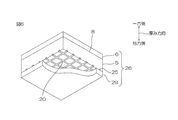
- the probe-containing sheet 26 is prepared.
- the probe-containing sheet 26 is formed on the second release sheet 29, the probe pattern 25 formed on one side in the thickness direction of the second release sheet 29, and on the one side in the thickness direction of the second release sheet 29, A pressure-sensitive adhesive layer 5 to be embedded and a base material layer 6 disposed on one surface in the thickness direction of the pressure-sensitive adhesive layer 5 are provided.
- the second release sheet 29 has the same configuration as the first release sheet 19 described above.
- the probe pattern 25 has the same pattern shape as the probe 8, and the material of the probe pattern 25 is the same as the material of the probe 8.
- the probe pattern 25 has a larger planar area than an imaginary circle passing through the outer surface 22 of the probe 8.
- Each of the pressure-sensitive adhesive layer 5 and the substrate layer 6 in the probe-containing sheet 26 has the same configuration as each of the pressure-sensitive adhesive layer 5 and the substrate layer 6 described above.
- the probe-containing sheet 26 is prepared, for example, by the methods described in JP-A-2017-22236 and JP-A-2017-22237.
- the cutting lines 27 are formed on the probe pattern 25, the pressure-sensitive adhesive layer 5 and the base layer 6 in a substantially circular shape in plan view.
- the cutting line 27 is formed by, for example, punching.
- the cutting line 27 divides the probe pattern 25, the pressure-sensitive adhesive layer 5 and the base layer 6 into and out of the same, but is not formed on the second release sheet 29.
- the dimensions of the cutting line 27 are the same as the inner diameters of the first opening 11 and the second opening 13. That is, the cutting line 27 coincides with an imaginary circle passing through the outer side surface 22.
- the formation of the cutting line 27 forms the probe member 18.
- the outer side surface 22 of the probe 8 is flush with the outer side surface of the pressure sensitive adhesive layer 5. In the probe member 18, the outer side surface 22 is exposed radially outward from the outer side surface of the pressure-sensitive adhesive layer 5.
- the probe member 18 is pulled up from the second release sheet 29. Specifically, the other surface in the thickness direction of the probe member 18 is peeled off from the second peeling sheet 29.
- the probe member 18 is fitted into the opening 23.
- connection portion 9 is provided in the second opening 13 and the first opening 11.
- the conductive resin composition (conductive composition liquid) is injected (or applied) to the second opening 13 and the first opening 11 Do. Thereafter, the conductive resin composition (conductive composition liquid) is heated to remove the solvent, and at the same time, the binder resin is crosslinked by the crosslinking agent.
- the laminated body 30 for biosensors provided with the base material 2 and the 1st peeling sheet 19 is produced.
- the biosensor stack 30 does not include the electronic component 3 (further, the battery 45), that is, it is not an adhesive type biosensor 1 but an intermediate component for manufacturing the adhesive type biosensor 1 .
- the plurality of electronic components 3 are mounted on the biosensor stack 30. Specifically, the terminal (not shown) of electronic component 3 is brought into contact with the component terminal (not shown) in wiring layer 7, and the other surface in the thickness direction of electronic component 3 is made the thickness of base material layer 6 Contact with one side of the direction.
- the sticking type biosensor 1 including the base 2, the electronic component 3 and the first release sheet 19 is manufactured.
- the patch-type biosensor 1 preferably includes only the base 2, the electronic component 3, and the first release sheet 19.
- the battery 45 is mounted on the patch-type biosensor 1 as shown by the phantom line in FIG. 1.
- the battery 45 has a substantially flat (box) shape extending in the surface direction.
- the battery 45 has a terminal (not shown) provided on the other surface in the thickness direction.
- the terminal (not shown) of the battery 45 is electrically connected to the battery terminal (not shown) of the wiring layer 7. At that time, the other surface in the thickness direction of the battery 45 is brought into contact with one surface in the thickness direction of the base material layer 6.
- the first release sheet 19 (see the arrow and the phantom line in FIG. 3D) is removed from the base 2 and the base 2 is attached to the skin 50.
- one longitudinal end edge of the first release sheet 19 (a portion of the first release sheet 19 facing the longitudinal end edge of the base material 2)
- the one longitudinal side portion of the first release sheet 19 is peeled away from the one longitudinal side portion of the substrate 2 while being peeled.
- the longitudinal direction one side portion of the thickness direction other surface (pressure-sensitive adhesive surface) of the base material 2 is exposed toward the other thickness direction side.
- the other surface (pressure-sensitive adhesive surface) in the thickness direction of the substrate 2 is pressure-sensitively adhered to the surface of the skin 50.
- the other longitudinal side portion of the first release sheet 19 is peeled off from the other longitudinal side portion of the substrate 2, and the other longitudinal side portion of the substrate 2 is Is exposed, and immediately thereafter, the portion is pressure-sensitively adhered to the surface of the skin 50.
- the first release sheet 19 is removed from the patch-type biosensor 1, and the other surface (pressure-sensitive adhesive surface) of the base 2 in the thickness direction is adhered to the surface of the skin 50.
- the probe 8 senses as an electrical signal from a living body, and the electrical signal sensed by the probe 8 is input to the electronic component 3 through the connection portion 9 and the wiring layer 7.
- the electronic component 3 processes the electrical signal based on the power supplied from the battery 45 and stores it as information. Furthermore, if necessary, the electric signal is converted into a radio wave, which is wirelessly transmitted to an external receiver.
- the operation of the first component 31, the second component 32, and the third component 33 in the electronic component 3 is as follows. If the sticking type biosensor 1 is a sticking type electrocardiograph (described later), the potential change of the heart acquired by the probe 8 is converted into digital data by the first component 31 which is an analog front end, and the second component which is a memory Record potential changes in the heart at 32. As an example, the potential change of the heart is recorded in the second part 32 at a data rate of 16 bits and 1 kHz. In addition, the third component 33 which is a communication IC wirelessly transmits the signal acquired by the probe 8 to the outside.
- the sticking type biosensor 1 is a sticking type electrocardiograph (described later)
- the potential change of the heart acquired by the probe 8 is converted into digital data by the first component 31 which is an analog front end
- the second component which is a memory Record potential changes in the heart at 32.
- the potential change of the heart is recorded in the second part 32 at a data rate of 16 bits and 1 kHz.
- the patch-type biosensor 1 After the above operation (that is, after sensing of the living body by the patch-type biosensor 1), the patch-type biosensor 1 is removed from the skin 50, and the recorded data is extracted from the second part 32 and analyzed. Thereafter, the second part 32 (and, if necessary, the first part 31 and the third part 33) is reused.
- the longitudinal direction LD of the electronic component 3 is orthogonal to the longitudinal direction of the base 2, the stress applied to the electronic component 3 can be reduced more reliably.
- the adhesive type biosensor 1 since the longitudinal direction LD of the electronic component 3 intersects with the longitudinal direction of the base 2, even when the first release sheet 19 is peeled from the base 2 The stress applied to the electronic component 3 can be reduced. Therefore, when the substrate 2 is attached to the skin 50, damage to the electronic component 3 can be further reliably suppressed.
- the plurality of electronic components 3 having the longitudinal direction LD along the longitudinal direction of the substrate 2 and arranged adjacent to the longitudinal direction of the substrate 2 are the substrate 2 described above as shown in FIGS. 12 and 13.
- the deformation along the longitudinal direction may cause contact with each other and damage due to this (Comparative Example 2). Specifically, damage due to the contact of the first part 31 and the second part 32 or the contact of the second part 32 and the third part 33 is assumed.
- this sticking type biosensor 1 at least one selected from the group consisting of an analog front end, a microcomputer, a memory, an interposer and a chip is hard or brittle, so the electronic component 3 is damaged when stressed. May occur.
- the adhesive type biosensor 1 since the longitudinal direction LD of the electronic component 3 intersects with the longitudinal direction of the base 2, the stress applied to the electronic component 3 can be reduced.
- the electronic component 3 is provided with the first component 31 which is an analog front end, the second component 32 which is a memory, and the third component 33 which is a communication IC, The sensing performance of the sensor 1 can be improved.
- the patch-type biosensor 1 is not particularly limited as long as it is a device capable of monitoring the state of a living body by sensing an electrical signal from the living body, for example.
- a patch-type electrocardiograph, a patch-type electroencephalograph And a patch-type sphygmomanometer, a patch-type pulsimeter, a patch-type electromyograph, a patch-type thermometer, and a patch-type accelerometer may be individual devices or a plurality of devices may be incorporated in one device.
- the patch-type biosensor 1 is preferably used as a patch-type electrocardiograph.
- the probe 8 senses the action potential of the heart as an electrical signal.
- a living body includes living bodies other than a human body and a human body, Preferably, it is a human body.
- the patch-type biosensor 1 may not include the first release sheet 19 and may include the base 2, the electronic component 3 and (only).
- the patch-type biosensor 1 includes a first release sheet 19, a base 2, and an electronic component 3.
- the first release sheet 19 can protect the pressure-sensitive adhesive surface of the substrate 2 from scratches, dust, and the like.
- FIG. 3B when the first release sheet 19 is removed along the longitudinal direction of the substrate 2, the substrate 2 tends to be deformed.
- the stress applied to the electronic component 3 is reduced even when the first release sheet 19 is peeled from the base material 2 be able to.
- the longitudinal direction LD of the electronic component 3 may cross the longitudinal direction of the substrate 2, that is, although not shown, the longitudinal direction LD of the electronic component 3 is orthogonal to the longitudinal direction of the substrate 2 although it does not, it may cross.
- the longitudinal directions LD of the plurality of electronic components 3 are inclined with respect to the longitudinal direction of the substrate 2.
- the angle between the longitudinal direction LD of the electronic component 3 and the longitudinal direction of the base material 2 is, for example, more than 0 degrees, and further 30 degrees or more, and for example, less than 90 degrees and less than 60 degrees.
- the longitudinal direction LD crossing (orthogonal to) the longitudinal direction of the substrate 2 may be provided with the electronic component 3, for example, one of the plurality of electronic components 3 with respect to the longitudinal direction of the substrate 2
- the other may have a longitudinal direction LD along the longitudinal direction of the substrate 2.
- the longitudinal direction LD of one or more of the electronic components 3 intersects (orthogonalizes) the longitudinal direction of the base material 2, preferably more than half of the electronic components 3.
- the longitudinal direction LD of the component 3 intersects (orthogonal to) the longitudinal direction of the substrate 2, and more preferably, the longitudinal direction LD of the electronic component 3 of 80% or more intersects the longitudinal direction of the substrate 2 More preferably, the longitudinal directions LD of all the electronic components 3 intersect (orthogonal) the longitudinal direction of the substrate 2.
- the arrangement of the plurality of electronic components 3 is not limited to the above, and examples thereof include the arrangements shown in FIGS. 9B to 9H.
- the plurality of electronic components 3 are spaced apart in the lateral direction of the substrate 2 It is done.
- the plurality of electronic components 3 are disposed at the center of the base 2 in the short direction.
- Each of the short direction end edges of the substrate 2 extends in a straight line along the longitudinal direction of the substrate 2 across the longitudinal central portion 46 and the longitudinal ends.
- the plurality of electronic components 3 are arranged spaced apart from each other in both the longitudinal direction and the lateral direction of the substrate 2.
- the electronic component 3 includes the first component 31, the second component 32 and the third component 33, and the second component 32 which are disposed apart from each other in the longitudinal direction.
- the fourth part 34 and the fifth part 35 are disposed at intervals on both sides in the short direction.
- the first part 31 and the second part 32 are disposed at an interval in the longitudinal direction of the base 2, and the third part 33 and the fourth part 34 are also of the base 2. It is spaced apart in the longitudinal direction.
- Each of the third component 33 and the fourth component 34 is disposed opposite to the first component 31 and the second component 32 at an interval on the other side in the short direction.
- the plurality of electronic components 3 are arranged offset from one another.
- the first part 31 and the third part 33 are shifted with the second part 32 and the fourth part 34 when projected in the longitudinal direction of the base material 2 and do not overlap.
- one side of the base 2 is short.
- they are arranged in order from the other side to the one side in the longitudinal direction of the base material 2.
- FIGS. 9A to 9H those are preferably the modifications shown in FIGS. 9B, 9D, 9F, 9G, and 9H, and more preferably the modifications shown in FIGS. 9B, 9F, and 9H. is there.
- the patch-type biosensor is used, for example, in a patch-type electrocardiograph, a patch-type electroencephalograph, a patch-type sphygmomanometer, a patch-type pulsimeter, a patch-type electromyograph, a patch-type thermometer, a patch-type accelerometer, and the like.
Abstract
The adhering-type biosensor according to the present invention is provided with: a substrate for adhering to an organism surface, the substrate extending in a longitudinal direction and having elastic properties; and an electronic component disposed on one surface of the substrate in the thickness direction thereof and extending in the longitudinal direction. The longitudinal direction of the electronic component intersects with the longitudinal direction of the substrate.
Description
本発明は、貼付型生体センサに関する。
The present invention relates to a patch-type biosensor.
従来、人の皮膚などに貼付することが可能な生体適合性ポリマー基板が知られている。
Conventionally, a biocompatible polymer substrate that can be attached to human skin or the like is known.
例えば、長手方向に延び、柔軟性を有するポリマー層と、その一方の面に固定されるデータ取得用モジュールとを備える生体適合性ポリマー基板が提案されている(例えば、特許文献1参照。)。
For example, a biocompatible polymer substrate has been proposed which comprises a longitudinally extending flexible layer and a data acquisition module fixed on one side thereof (see, for example, Patent Document 1).
上記特許文献1の生体適合性ポリマー基板では、データ取得用モジュールは、ポリマー層の長手方向と同じ方向に長く延びている。そのため、上記特許文献1の生体適合性ポリマー基板を、ポリマー層の長手方向に沿って人の皮膚に貼付するときに、柔軟性を有するポリマー層において、長手方向に沿って屈曲(あるいは湾曲)などの変形を生じる。その際、ポリマー層の変形に起因して、データ取得用モジュールに大きな応力がかかり、データ取得用モジュールが損傷するという不具合がある。
In the biocompatible polymer substrate of Patent Document 1, the data acquisition module extends in the same direction as the longitudinal direction of the polymer layer. Therefore, when the biocompatible polymer substrate of Patent Document 1 is applied to human skin along the longitudinal direction of the polymer layer, bending (or bending) or the like along the longitudinal direction in the flexible polymer layer Results in At that time, due to the deformation of the polymer layer, a large stress is applied to the data acquisition module, and there is a problem that the data acquisition module is damaged.
本発明は、基材を生体表面に貼付するときに、電子部品の損傷を抑制することのできる貼付型生体センサを提供する。
The present invention provides a patch-type biosensor capable of suppressing damage to an electronic component when the substrate is affixed to the surface of a living body.
本発明(1)は、長手方向に延び、伸縮性を有し、生体表面に貼付するための基材と、前記基材の厚み方向一方面に配置され、長手方向に延びる電子部品とを備え、前記電子部品の長手方向が、前記基材の長手方向と交差する、貼付型生体センサを含む。
The present invention (1) comprises a base material extending in the longitudinal direction and having stretchability and being attached to the surface of a living body, and an electronic component disposed on one surface in the thickness direction of the base material and extending in the longitudinal direction. And a patch-type biosensor, wherein the longitudinal direction of the electronic component intersects with the longitudinal direction of the substrate.
基材をその長手方向に沿って生体表面に貼着して、基材がその長手方向に沿って変形しても、この貼付型生体センサでは、電子部品の長手方向が、基材の長手方向と交差するので、電子部品にかかる応力を低減することができる。そのため、基材を生体表面に貼付するときに、電子部品の損傷を抑制することができる。
Even if the substrate is attached to the surface of the living body along its longitudinal direction and the substrate is deformed along its longitudinal direction, in this attachment type biosensor, the longitudinal direction of the electronic component is the longitudinal direction of the substrate And the stress applied to the electronic component can be reduced. Therefore, when the substrate is attached to the surface of the living body, damage to the electronic component can be suppressed.
本発明(2)は、前記電子部品の長手方向が、前記基材の長手方向と直交する、(1)に記載の貼付型生体センサを含む。
The present invention (2) includes the adhesive biosensor as described in (1), in which the longitudinal direction of the electronic component is orthogonal to the longitudinal direction of the substrate.
基材をその長手方向に沿って生体表面に貼着して、基材がその長手方向に沿って変形しても、この貼付型生体センサでは、電子部品の長手方向が、基材の長手方向と直交するので、電子部品にかかる応力をより一層確実に低減することができる。そのため、基材を生体表面に貼付するときに、電子部品の損傷をより一層確実に抑制することができる。
Even if the substrate is attached to the surface of the living body along its longitudinal direction and the substrate is deformed along its longitudinal direction, in this attachment type biosensor, the longitudinal direction of the electronic component is the longitudinal direction of the substrate And the stress applied to the electronic component can be further reliably reduced. Therefore, when the substrate is attached to the surface of the living body, damage to the electronic component can be more reliably suppressed.
本発明(3)は、前記基材の前記厚み方向他方面に配置され、前記基材の長手方向に沿って剥離される剥離シートをさらに備える、(1)または(2)に記載の貼付型生体センサを含む。
The present invention (3) is the patch type according to (1) or (2), further comprising a release sheet which is disposed on the other surface in the thickness direction of the substrate and which is peeled along the longitudinal direction of the substrate Includes a biometric sensor.
剥離シートを、基材の長手方向に沿って剥離するときにも、基材は、伸縮性を有することから、変形を生じ易い。
Even when the release sheet is released along the longitudinal direction of the substrate, the substrate is likely to be deformed because it has stretchability.
しかし、上記したように、この貼付型生体センサでは、電子部品の長手方向が基材の長手方向と交差するので、剥離シートを基材から剥離するときにも、電子部品にかかる応力を低減することができる。
However, as described above, in this patch-type biosensor, since the longitudinal direction of the electronic component intersects with the longitudinal direction of the substrate, stress applied to the electronic component is reduced even when the release sheet is peeled from the substrate be able to.
本発明(4)は、前記電子部品は、前記基材の長手方向に沿って隣接配置される少なくとも2つの前記電子部品を含む、(1)~(3)のいずれか一項に記載の貼付型生体センサを含む。
In the invention (4), the electronic component includes at least two of the electronic components disposed adjacent to each other along the longitudinal direction of the substrate, according to any one of (1) to (3) Type biometric sensor.
隣接配置される少なくとも2つの電子部品は、上記した基材の長手方向に沿う変形によって、互いに接触して、損傷する場合がある。
At least two electronic components arranged adjacent to each other may be damaged by contact with each other due to the deformation along the longitudinal direction of the above-mentioned substrate.
しかし、この貼付型生体センサでは、電子部品の長手方向が、基材の長手方向と交差するので、上記した接触の発生を抑制して、電子部品の損傷を抑制することができる。
However, in this patch-type biosensor, since the longitudinal direction of the electronic component intersects with the longitudinal direction of the base material, the occurrence of the above-described contact can be suppressed, and damage to the electronic component can be suppressed.
本発明(5)は、前記基材の長手方向における前記2つの前記電子部品間の間隔Iの、前記電子部品の最大厚みTmaxに対する比(I/Tmax)が、2以上である、(4)に記載の貼付型生体センサを含む。
In the invention (5), the ratio (I / Tmax) of the distance I between the two electronic components in the longitudinal direction of the substrate to the maximum thickness Tmax of the electronic components is 2 or more. And a patch-type biosensor as described in the above.
基材の長手方向における2つの電子部品間の間隔Iの、電子部品の最大厚みTmaxに対する比I/Tmax)が、2以上であるので、2つの電子部品が互いに接触することを有効に抑制して、電子部品の損傷を有効に抑制することができる。
Since the ratio I / Tmax of the distance I between two electronic components in the longitudinal direction of the substrate to the maximum thickness Tmax of the electronic component is 2 or more, the two electronic components are effectively inhibited from contacting each other Thus, damage to the electronic component can be effectively suppressed.
本発明(6)は、前記電子部品が、アナログフロントエンド、マイコン、メモリ、インターポーザおよびチップからなる群からなる選択される少なくとも1つである、(1)~(5)のいずれか一項に記載の貼付型生体センサを含む。
The present invention (6) is any one of (1) to (5), wherein the electronic component is at least one selected from the group consisting of an analog front end, a microcomputer, a memory, an interposer and a chip. It includes the attached type biosensor as described.
この貼付型生体センサでは、アナログフロントエンド、マイコン、メモリ、インターポーザおよびチップからなる群からなる選択される少なくとも1つは、硬く、あるいは、脆く、そのため、電子部品は、応力を受けると損傷を生じる場合がある。
In this patch-type biosensor, at least one selected from the group consisting of an analog front end, a microcomputer, a memory, an interposer and a chip is hard or brittle, so the electronic component is damaged when it is stressed There is a case.
しかし、この貼付型生体センサでは、上記したように、電子部品の長手方向が、基材の長手方向と交差するので、電子部品にかかる応力を低減することができる。
However, in the patch-type biosensor, as described above, since the longitudinal direction of the electronic component intersects with the longitudinal direction of the base, stress applied to the electronic component can be reduced.
さらに、電子部品が、アナログフロントエンド、マイコン、メモリ、インターポーザおよびチップからなる群からなる選択される少なくとも1つであるので、その作動によって、貼付型生体センサのセンシング性能を向上させることができる。
Furthermore, since the electronic component is at least one selected from the group consisting of an analog front end, a microcomputer, a memory, an interposer and a chip, its operation can improve the sensing performance of the patch-type biosensor.
この貼付型生体センサは、基材を生体表面に貼付するときに、電子部品の損傷を抑制することができる。
The patch-type biosensor can suppress damage to the electronic component when the substrate is stuck to the surface of the living body.
本発明の貼付型生体センサの一実施形態を、図1~図4を参照して説明する。
One embodiment of a patch-type biosensor according to the present invention will be described with reference to FIGS. 1 to 4.
なお、図3A~図3Dにおいて、後述するが、電子部品3が備える各層など(例えば、感圧接着層5や基材層6など)は、電子部品3の側面視形状を明確に示すために、省略している。
3A to 3D, although it will be described later, layers or the like included in the electronic component 3 (for example, the pressure-sensitive adhesive layer 5 and the base material layer 6) clearly show the side view shape of the electronic component 3. Is omitted.
図1および図2に示すように、貼付型生体センサ1は、長手方向に延びる略平板形状を有する。貼付型生体センサ1は、基材2と、基材2の厚み方向一方面に配置される電子部品3とを備える。
As shown in FIG. 1 and FIG. 2, the sticking type biosensor 1 has a substantially flat plate shape extending in the longitudinal direction. The sticking type biosensor 1 includes a base 2 and an electronic component 3 disposed on one surface of the base 2 in the thickness direction.
基材2は、回路部付き貼付用基材であって、例えば、回路部36(後述)を有しながら、伸縮性(柔軟性)および感圧接着性も有する基材である。基材2は、長手方向に延びる平板形状であって、優れた伸縮性を有するシートである。具体的には、基材2は、長手方向に延びる帯状を有し、長手方向中央部46が短手方向(長手方向および厚み方向に直交する方向)(幅方向)両外側に向かって膨らむ形状を有する。
The base material 2 is a base material for attachment with a circuit part, and for example, is a base material having stretchability (flexibility) and pressure-sensitive adhesiveness while having a circuit part 36 (described later). The substrate 2 is a flat plate extending in the longitudinal direction, and is a sheet having excellent stretchability. Specifically, the base material 2 has a strip extending in the longitudinal direction, and the longitudinal central portion 46 bulges outward in the lateral direction (direction orthogonal to the longitudinal direction and the thickness direction) (width direction) Have.
また、基材2は、感圧接着層5と、基材層6と、配線層7と、プローブ8と、接続部9とを備える。
Further, the base 2 includes the pressure-sensitive adhesive layer 5, the base layer 6, the wiring layer 7, the probe 8, and the connection portion 9.
感圧接着層5は、基材2の厚み方向他方面(感圧接着面)を形成する。つまり、感圧接着層5は、基材2を生体表面(図4における皮膚50など)に対して貼付するために、貼付型生体センサ1の厚み方向他方面に感圧接着性を付与する層である。感圧接着層5は、基材2の外形形状を形成している。感圧接着層5は、長手方向に延びる平板形状を有する。
The pressure-sensitive adhesive layer 5 forms the other surface (pressure-sensitive adhesive surface) in the thickness direction of the substrate 2. That is, the pressure-sensitive adhesive layer 5 is a layer that imparts pressure-sensitive adhesiveness to the other surface of the stick-type biosensor 1 in the thickness direction in order to stick the substrate 2 to the surface of the living body (such as the skin 50 in FIG. 4). It is. The pressure sensitive adhesive layer 5 forms the outer shape of the substrate 2. The pressure sensitive adhesive layer 5 has a flat plate shape extending in the longitudinal direction.
感圧接着層5は、その長手方向両端部に、2つの第1開口部11を有する。2つの第1開口部11のそれぞれは、平面視略リング形状を有する。第1開口部11は、感圧接着層5の厚み方向を貫通する。また、第1開口部11の内側における厚み方向他方面は、厚み方向他方側に向かって開放され、プローブ8に対応する第1溝10を有する。
The pressure-sensitive adhesive layer 5 has two first openings 11 at both longitudinal ends. Each of the two first openings 11 has a substantially ring shape in plan view. The first opening 11 penetrates the thickness direction of the pressure-sensitive adhesive layer 5. Further, the other surface in the thickness direction on the inner side of the first opening 11 is opened toward the other side in the thickness direction, and has a first groove 10 corresponding to the probe 8.
感圧接着層5の材料としては、例えば、感圧接着性を有する材料であれば特に限定されない。また、感圧接着層5は、伸縮性を有する伸縮性材料でもある。
The material of the pressure-sensitive adhesive layer 5 is not particularly limited as long as the material has pressure-sensitive adhesion, for example. The pressure-sensitive adhesive layer 5 is also an elastic material having elasticity.
基材層6は、基材2の厚み方向一方面を形成する。基材層6は、感圧接着層5とともに基材2の外形形状(厚み方向に投影した形状)を形成している。基材層6の平面視形状は、感圧接着層5の平面視形状と同一である。基材層6は、感圧接着層5の厚み方向一方面全面に配置されている。基材層6は、感圧接着層5を支持する支持層である。基材層6は、長手方向に延びる平板形状を有する。
The base layer 6 forms one surface in the thickness direction of the base 2. The base layer 6 forms the outer shape (the shape projected in the thickness direction) of the base 2 together with the pressure-sensitive adhesive layer 5. The plan view shape of the base material layer 6 is the same as the plan view shape of the pressure sensitive adhesive layer 5. The base layer 6 is disposed on the entire surface in the thickness direction of the pressure-sensitive adhesive layer 5. The base layer 6 is a support layer that supports the pressure-sensitive adhesive layer 5. The base layer 6 has a flat plate shape extending in the longitudinal direction.
また、基材層6は、その厚み方向一方面において、配線層7(後述)に対応する第2溝12を有する。第2溝12は、平面視において、配線層7と同一のパターン形状を有する。第2溝12は、厚み方向一方側に向かって開放される。
Moreover, the base material layer 6 has the 2nd groove | channel 12 corresponding to the wiring layer 7 (after-mentioned) in the thickness direction one surface. The second groove 12 has the same pattern shape as the wiring layer 7 in plan view. The second groove 12 is opened toward one side in the thickness direction.
また、基材層6は、第1開口部11に対応する第2開口部13を有する。第2開口部13は、第1開口部11に厚み方向に連通する。第2開口部13は、第1開口部11と同一形状および同一寸法の平面視略リング形状を有する。
The base layer 6 also has a second opening 13 corresponding to the first opening 11. The second opening 13 communicates with the first opening 11 in the thickness direction. The second opening 13 has a substantially ring shape in plan view having the same shape and the same size as the first opening 11.
基材層6の材料は、例えば、伸縮性を有する絶縁体などが挙げられる。そのような材料としては、例えば、ポリウレタン系樹脂などの樹脂が挙げられる。
Examples of the material of the base layer 6 include an insulator having stretchability. As such a material, resin, such as polyurethane-type resin, is mentioned, for example.
基材層6の破断伸度は、例えば、100%以上、好ましくは、200%以上、より好ましくは、300%以上であり、また、例えば、2000%以下である。破断伸度が上記下限以上であれば、基材層6の材料が優れた伸縮性を有する。
The breaking elongation of the base material layer 6 is, for example, 100% or more, preferably 200% or more, more preferably 300% or more, and for example, 2000% or less. If the breaking elongation is at least the above lower limit, the material of the base material layer 6 has excellent stretchability.
配線層7は、例えば、第2溝12に埋め込まれている。詳しくは、配線層7は、その厚み方向一方面が基材層6から露出するように、基材層6の厚み方向一方側部に埋め込まれている。配線層7の厚み方向一方面は、基材層6の厚み方向一方面および電子部品3とともに、基材2の厚み方向一方面を形成する。
The wiring layer 7 is embedded in, for example, the second groove 12. Specifically, the wiring layer 7 is embedded in one side of the base layer 6 in the thickness direction such that one side in the thickness direction is exposed from the base layer 6. The thickness direction one surface of the wiring layer 7 forms the thickness direction one surface of the base material 2 together with the thickness direction one surface of the base material layer 6 and the electronic component 3.
配線層7は、接続部9と、電子部品3(後述)とを接続する配線パターンを有する。配線層7は、電子部品3との電気的な接続に用いられる部品用端子(図示せず)を含む。
The wiring layer 7 has a wiring pattern for connecting the connection portion 9 and the electronic component 3 (described later). Wiring layer 7 includes component terminals (not shown) used for electrical connection with electronic component 3.
なお、配線層7の幅(線幅)は、基材層6の伸縮性を阻害しないような範囲に設定されており、例えば、2000μm以下、好ましくは、500μm以下であり、また、例えば、50μm以上、好ましくは、200μm以上である。
The width (line width) of the wiring layer 7 is set in a range that does not inhibit the stretchability of the base layer 6, and is, for example, 2000 μm or less, preferably 500 μm or less, or, for example, 50 μm. The above, preferably, 200 μm or more.
配線層7の材料としては、例えば、銅、ニッケル、金、それらの合金などの導体が挙げられる。配線層7の材料として、好ましくは、銅が挙げられる。
Examples of the material of the wiring layer 7 include conductors such as copper, nickel, gold, and their alloys. As a material of the wiring layer 7, preferably, copper is mentioned.
プローブ8は、図4に示すように、感圧接着層5が皮膚50に貼付されるときに、皮膚50に接触して、生体からの電気信号や温度、振動、汗、代謝物などをセンシングする電極(生体電極)である。プローブ8は、感圧接着層5の厚み方向他方面から露出するように、感圧接着層5に埋め込まれている。つまり、プローブ8は、第1開口部11の内側において、感圧接着層5における第1溝10に埋め込まれている。なお、プローブ8は、第1溝10を形成する感圧接着層5の厚み方向他方面に配置されている。プローブ8は、感圧接着層5とともに、基材2の厚み方向他方面を形成する。プローブ8は、網形状、好ましくは、平面視略碁盤目形状(あるいは略メッシュ形状)を有する。なお、図8に示すように、プローブ8の側面のうち、最外側に位置する外側面は、平面視において、それらを通過する仮想円を形成する。プローブ8の材料としては、配線層7で例示した材料(具体的には、導体)が挙げられる。プローブ8の外形寸法は、外側面22を通過する仮想円が、第1開口部11を区画する内周面が平面視で重複するように、設定されている。
The probe 8 contacts the skin 50 when the pressure-sensitive adhesive layer 5 is attached to the skin 50 as shown in FIG. 4, and senses the electrical signal from the living body, temperature, vibration, sweat, metabolites, etc. Electrode (bioelectrode). The probe 8 is embedded in the pressure sensitive adhesive layer 5 so as to be exposed from the other surface in the thickness direction of the pressure sensitive adhesive layer 5. That is, the probe 8 is embedded in the first groove 10 in the pressure-sensitive adhesive layer 5 inside the first opening 11. The probe 8 is disposed on the other surface of the pressure-sensitive adhesive layer 5 forming the first groove 10 in the thickness direction. The probe 8 forms the other surface of the base 2 in the thickness direction together with the pressure-sensitive adhesive layer 5. The probe 8 has a net shape, preferably a substantially grid shape in plan view (or a substantially mesh shape). In addition, as shown in FIG. 8, the outer side surface located in the outermost side among the side surfaces of the probe 8 forms the virtual circle which passes them in planar view. Examples of the material of the probe 8 include the materials (specifically, conductors) exemplified for the wiring layer 7. The outer dimensions of the probe 8 are set such that the virtual circle passing through the outer side surface 22 overlaps the inner peripheral surface defining the first opening 11 in plan view.
図1および図2に示すように、接続部9は、第2開口部13および第1開口部11に対応して設けられており、それらと同一形状を有する。接続部9は、基材層6および感圧接着層5を厚み方向に貫通(通過)しており、第2開口部13および第1開口部11に充填されている。接続部9は、図8Bに示すように、プローブ8の外側面22に沿う、平面視無端形状を有する。具体的には、接続部9は、軸線が厚み方向に延びる(外側面22を通過する仮想円に沿う)略円筒形状を有する。
As shown in FIGS. 1 and 2, the connection portion 9 is provided corresponding to the second opening 13 and the first opening 11 and has the same shape as them. The connection portion 9 penetrates (passes) the base material layer 6 and the pressure-sensitive adhesive layer 5 in the thickness direction, and is filled in the second opening 13 and the first opening 11. The connection portion 9 has an endless shape in plan view along the outer side surface 22 of the probe 8 as shown in FIG. 8B. Specifically, the connection portion 9 has a substantially cylindrical shape in which an axis extends in the thickness direction (along an imaginary circle passing through the outer side surface 22).
接続部9の内側面は、プローブ8の外側面22に接触している。接続部9は、第1開口部11の外側の感圧接着層5と、第1開口部11の内側の感圧接着層5とに感圧接着している。また、接続部9は、第2開口部13の外側の基材層6と、第2開口部13の内側の基材層6とに接触している。
The inner surface of the connection portion 9 is in contact with the outer surface 22 of the probe 8. The connection portion 9 is pressure-sensitively adhered to the pressure-sensitive adhesive layer 5 outside the first opening 11 and the pressure-sensitive adhesive layer 5 inside the first opening 11. The connecting portion 9 is in contact with the base layer 6 outside the second opening 13 and the base layer 6 inside the second opening 13.
接続部9の厚み方向一方面は、基材層6の厚み方向一方面と面一である。接続部9の厚み方向他方面は、感圧接着層5の厚み方向他方面と面一である。
The thickness direction one surface of the connection portion 9 is flush with the thickness direction one surface of the base material layer 6. The other surface in the thickness direction of the connection portion 9 is flush with the other surface in the thickness direction of the pressure-sensitive adhesive layer 5.
図1に示すように、2つの接続部9のうち、長手方向一方側に位置する接続部9は、その厚み方向一端部において、長手方向一方側に位置する配線層7の長手方向一端部に連続する。長手方向他方側に位置する接続部9は、その厚み方向一端部において、長手方向他方側に位置する配線層7の長手方向他端縁に連続する。つまり、接続部9は、配線層7と電気的に接続される。
As shown in FIG. 1, of the two connection portions 9, the connection portion 9 located on one side in the longitudinal direction is one end of the wiring layer 7 located on one side in the longitudinal direction at one end in the thickness direction. Be continuous. The connecting portion 9 located on the other side in the longitudinal direction is continuous with the other end edge in the longitudinal direction of the wiring layer 7 located on the other side in the longitudinal direction at one end in the thickness direction. That is, the connection portion 9 is electrically connected to the wiring layer 7.
これにより、接続部9は、配線層7とプローブ8とを電気的に接続する。
Thus, the connection portion 9 electrically connects the wiring layer 7 and the probe 8.
接続部9の材料としては、例えば、金属、導電性樹脂(導電性高分子を含む)などが挙げられ、好ましくは、導電性樹脂などが挙げられる。
As a material of the connection part 9, a metal, electroconductive resin (including electroconductive polymer), etc. are mentioned, for example, Preferably, electroconductive resin etc. are mentioned.
なお、接続部9および配線層7は、プローブ8を電子部品3に電気的に接続する回路部36を構成する。つまり、回路部36は、基材2の厚み方向一方面に配置される配線層7と、基材2を厚み方向に通過する接続部9とを備える。好ましくは、回路部36は、配線層7および接続部9のみからなる。
The connection portion 9 and the wiring layer 7 constitute a circuit portion 36 which electrically connects the probe 8 to the electronic component 3. That is, the circuit portion 36 includes the wiring layer 7 disposed on one surface of the base 2 in the thickness direction, and the connection portion 9 passing the base 2 in the thickness direction. Preferably, the circuit portion 36 is formed only of the wiring layer 7 and the connection portion 9.
電子部品3としては、例えば、プローブ8で取得した生体からの電気信号として処理して記憶するためのアナログフロントエンド、マイコン、メモリなどのロジックIC、さらには、電気信号を電波に変換し、これを外部の受信機に無線送信するための通信ICなどの送信機、さらには、インターポーザなどが挙げられる。
As the electronic component 3, for example, an analog front end for processing and storing as an electric signal from a living body acquired by the probe 8, a microcomputer, a logic IC such as a memory, and further convert the electric signal into a radio wave Transmitter such as a communication IC for wireless transmission to an external receiver, or an interposer.
電子部品3としては、上記した例示から単独または複数が適宜組み合わせて選択される。
As the electronic component 3, one or more may be selected appropriately from the above-described examples.
電子部品3は、基材2における長手方向中央部46において短手方向一方部に配置されている。電子部品3は、基材2の長手方向において互いに間隔を隔てて複数(例えば、3つ)整列配置されている。具体的には、電子部品3は、第1部品31、第2部品32および第3部品33を備え、これらは、基材2の長手方向他方側から一方側に向かって順に配置されている。例えば、第1部品31が、アナログフロントエンドであり、第2部品32が、メモリであり、第3部品33が、通信ICである。
The electronic component 3 is disposed at one longitudinal direction central portion 46 of the base 2 in the lateral direction. A plurality of (for example, three) electronic components 3 are arranged at intervals in the longitudinal direction of the substrate 2. Specifically, the electronic component 3 includes a first component 31, a second component 32, and a third component 33, which are arranged in order from the other side in the longitudinal direction of the base 2 to one side. For example, the first component 31 is an analog front end, the second component 32 is a memory, and the third component 33 is a communication IC.
複数の電子部品3のそれぞれは、電子部品3の長手方向LDに延びる。電子部品3の長手方向LDは、基材2の短手方向と交差しており、具体的には、基材2の短手方向と直交する。具体的には、複数の電子部品3のそれぞれは、基材2の短手方向に長く沿って延びる平面視略矩形状を有する。
Each of the plurality of electronic components 3 extends in the longitudinal direction LD of the electronic component 3. The longitudinal direction LD of the electronic component 3 intersects the short side direction of the base material 2, and specifically, is orthogonal to the short side direction of the base material 2. Specifically, each of the plurality of electronic components 3 has a substantially rectangular shape in plan view extending along a long direction of the base 2.
また、複数の電子部品3は、長手方向に投影したときに、重複する。
Further, the plurality of electronic components 3 overlap when projected in the longitudinal direction.
なお、複数の電子部品3の長手方向LDにおいて、基材2の短手方向一端縁に向かう側の一端縁37(長手方向一端縁)は、基材2の長手方向に投影したときに、同一位置に配置されている。
In the longitudinal direction LD of the plurality of electronic components 3, one end 37 (longitudinal one end edge) on the side facing the one end edge of the base 2 is the same when projected in the longitudinal direction of the base 2. It is placed in position.
電子部品3は、基材2の厚み方向一方面に配置されている。具体的には、電子部品3は、基材層6の厚み方向一方面に接触している。電子部品3は、断面視略矩平板形状を有する。電子部品3の厚み方向他方面には、端子(図示せず)が設けられる。電子部品3の端子(図示せず)は、配線層7の部品用端子(図示せず)と電気的に接続される。
The electronic component 3 is disposed on one surface of the base 2 in the thickness direction. Specifically, the electronic component 3 is in contact with one surface of the base layer 6 in the thickness direction. The electronic component 3 has a substantially rectangular plate shape in cross section. A terminal (not shown) is provided on the other surface of the electronic component 3 in the thickness direction. The terminal (not shown) of the electronic component 3 is electrically connected to the component terminal (not shown) of the wiring layer 7.
電子部品3は、例えば、感圧接着層5および基材層6に比べて、硬い。そのため、電子部品3の材料としては、例えば、硬質材料が挙げられ、例えば、ケイ素系無機材料が挙げられる。
The electronic component 3 is harder than, for example, the pressure sensitive adhesive layer 5 and the base material layer 6. Therefore, as a material of the electronic component 3, a hard material is mentioned, for example, For example, a silicon-type inorganic material is mentioned.
電子部品3の長手方向LDの長さLは、上記した幅Wを超過すれば特に限定されず、例えば、長手方向長さLの幅Wに対する比(L/W)が1を超過、好ましくは、1.2以上、より好ましくは、1.5以上、また、例えば、10以下となるように、設定される。電子部品3の長さLは、電子部品3の、基材2の短手方向における長さを意味する。
The length L of the longitudinal direction LD of the electronic component 3 is not particularly limited as long as it exceeds the above-mentioned width W. For example, the ratio (L / W) of the longitudinal length L to the width W exceeds 1, preferably , 1.2 or more, more preferably, 1.5 or more, and for example, 10 or less. The length L of the electronic component 3 means the length of the electronic component 3 in the short direction of the substrate 2.
電子部品3の厚みTは、例えば、20μm以上、好ましくは、50μm以上であり、また、例えば、3000μm以下、好ましくは、1000μm以下である。
The thickness T of the electronic component 3 is, for example, 20 μm or more, preferably 50 μm or more, and for example, 3000 μm or less, preferably 1000 μm or less.
また、隣接する電子部品3の最大厚みTmaxは、例えば、20μm以上、好ましくは、50μm以上であり、また、例えば、3000μm以下、好ましくは、1000μm以下である。なお、最大厚みTmaxは、厚みの異なる2つの電子部品3が隣接する場合において、厚い厚みを有する電子部品3の厚みを意味する。
The maximum thickness Tmax of the adjacent electronic component 3 is, for example, 20 μm or more, preferably 50 μm or more, and for example, 3000 μm or less, preferably 1000 μm or less. The maximum thickness Tmax means the thickness of the electronic component 3 having a large thickness when two electronic components 3 having different thicknesses are adjacent to each other.
隣接する電子部品3間の間隔Iは、例えば、40μm以上、好ましくは、100μm以上であり、また、例えば、6000μm以下、好ましくは、2000μm以下である。間隔Iは、隣接する電子部品3間における、基材2の短手方向における距離に相当する。
The spacing I between the adjacent electronic components 3 is, for example, 40 μm or more, preferably 100 μm or more, and for example, 6000 μm or less, preferably 2000 μm or less. The spacing I corresponds to the distance between the adjacent electronic components 3 in the short direction of the substrate 2.
そして、隣接する2つの電子部品3間の間隔Iの、2つの電子部品3の最大厚みTmaxに対する比(I/Tmax)は、例えば、2以上、好ましくは、2.5以上、より好ましくは、3以上であり、また、例えば、4以下である。
The ratio (I / Tmax) of the distance I between two adjacent electronic components 3 to the maximum thickness Tmax of the two electronic components 3 is, for example, 2 or more, preferably 2.5 or more, more preferably, It is three or more, for example, four or less.
上記した比(I/Tmax)が上記した下限以上であれば、複数の電子部品3を省スペースで(高密度)で配置することができる。
If the ratio (I / Tmax) described above is equal to or more than the lower limit described above, the plurality of electronic components 3 can be disposed with high efficiency and space saving.
一方、上記した比(I/Tmax)が上記した下限以上であれば、貼付型生体センサ1を皮膚50にする際に、2つの電子部品3同士が接触することを有効に抑制して、電子部品3の損傷を有効に抑制することができる。
On the other hand, when the ratio (I / Tmax) described above is equal to or more than the lower limit described above, when the adhesive biosensor 1 is made to be the skin 50, contact between the two electronic components 3 is effectively suppressed. Damage to the part 3 can be effectively suppressed.
電子部品3の幅Wは、電子部品3の長手方向LDに直交する方向の長さであり、電子部品3の、基材2の長手方向における長さに相当し、具体的には、5000μm以下、好ましくは、4000μm以下、より好ましくは、3000μm以下であり、また、例えば、1000μm以上である。幅Wが上記した上限以下であれば、基材2を皮膚50に貼付するときに、電子部品3に応力がかかったときの損傷を有効に抑制することができる。
The width W of the electronic component 3 is a length in the direction orthogonal to the longitudinal direction LD of the electronic component 3 and corresponds to the length of the electronic component 3 in the longitudinal direction of the base 2, specifically, 5000 μm or less Preferably, it is 4000 μm or less, more preferably, 3000 μm or less, and for example, 1000 μm or more. When the width W is equal to or less than the above-described upper limit, when the substrate 2 is attached to the skin 50, damage when the electronic component 3 is stressed can be effectively suppressed.
また、図2に示すように、貼付型生体センサ1は、剥離シートの一例としての第1剥離シート19を備える。第1剥離シート19は、貼付型生体センサ1における最下面を形成する。第1剥離シート19は、基材2の厚み方向他方面に配置されている。第1剥離シート19は、基材2の厚み方向他方面(感圧接着層5の感圧接着面)を被覆して、それを傷や埃などから保護する保護シートである。そして、第1剥離シート19は、貼付型生体センサ1の使用時(図3B~図3D参照)には、基材2の長手方向に沿って基材2から剥離される剥離可能シートである。
Moreover, as shown in FIG. 2, the sticking type biometric sensor 1 is provided with the 1st peeling sheet 19 as an example of a peeling sheet. The first release sheet 19 forms the lowermost surface of the adhesive type biosensor 1. The first release sheet 19 is disposed on the other surface of the base 2 in the thickness direction. The first release sheet 19 is a protective sheet that covers the other surface of the base 2 in the thickness direction (the pressure-sensitive adhesive surface of the pressure-sensitive adhesive layer 5) and protects it from scratches, dust, and the like. The first peelable sheet 19 is a peelable sheet which is peeled from the base 2 along the longitudinal direction of the base 2 when the attached biosensor 1 is in use (see FIGS. 3B to 3D).
第1剥離シート19は、例えば、基材2の長手方向に延びる略平板形状を有する。第1剥離シート19の材料としては、例えば、ポリエステル(ポリエチレンテレフタレートなど)、ポリオレフィン(ポリプロピレンなど)などの樹脂(高分子)、例えば、アルミニウム、ステンレスなどの金属が挙げられる。第1剥離シート19の材料としては、伸縮性の観点から、好ましくは、樹脂が挙げられる。
The first release sheet 19 has, for example, a substantially flat plate shape extending in the longitudinal direction of the substrate 2. Examples of the material of the first release sheet 19 include resins (polymers) such as polyester (such as polyethylene terephthalate) and polyolefins (such as polypropylene), and metals such as aluminum and stainless steel. The material of the first release sheet 19 is preferably a resin from the viewpoint of stretchability.
次に、貼付型生体センサ1の製造方法を図5A~図8を参照して説明する。
Next, a method of manufacturing the stick-type biosensor 1 will be described with reference to FIGS. 5A to 8.
この方法では、まず、基材2を、図5A~図5Dに従って、準備する。
In this method, first, a substrate 2 is prepared according to FIGS. 5A-5D.
基材2を準備するには、まず、図5Aに示すように、基材層6および配線層7を準備する。例えば、特開2017-22236号公報、特開2017-22237号公報に記載される方法によって、配線層7が第2溝12に埋め込まれるように、基材層6および配線層7を準備する。
In order to prepare the substrate 2, first, as shown in FIG. 5A, the substrate layer 6 and the wiring layer 7 are prepared. For example, the base material layer 6 and the wiring layer 7 are prepared such that the wiring layer 7 is embedded in the second groove 12 by the method described in JP-A-2017-22236 and JP-A-2017-22237.
次いで、図5Bに示すように、感圧接着層5を、基材層6の厚み方向他方面に配置する。感圧接着層5を配置するには、例えば、まず、感圧接着層5の材料を含有する塗布液を調製し、続いて、塗布液を、第1剥離シート19の厚み方向一方面に塗布し、その後、加熱により乾燥させる。これによって、感圧接着層5を第1剥離シート19の厚み方向一方面に配置する。
Next, as shown in FIG. 5B, the pressure-sensitive adhesive layer 5 is disposed on the other surface of the base layer 6 in the thickness direction. In order to dispose the pressure-sensitive adhesive layer 5, for example, first, a coating solution containing the material of the pressure-sensitive adhesive layer 5 is prepared, and then, the coating solution is applied to one surface of the first release sheet 19 in the thickness direction And then dried by heating. By this, the pressure sensitive adhesive layer 5 is disposed on one surface of the first release sheet 19 in the thickness direction.
次いで、感圧接着層5および基材層6を、例えば、ラミネータなどにより、貼り合わせる。具体的には、感圧接着層5の厚み方向一方面と、基材層6の厚み方向他方面とを接触させる。
Subsequently, the pressure-sensitive adhesive layer 5 and the base material layer 6 are attached to each other by, for example, a laminator. Specifically, one surface of the pressure-sensitive adhesive layer 5 in the thickness direction is brought into contact with the other surface of the base layer 6 in the thickness direction.
なお、この時点では、基材層6および感圧接着層5のそれぞれは、第2開口部13および第1開口部11(開口部23)のそれぞれ(図5C参照)を有しない。
At this point, each of the base material layer 6 and the pressure-sensitive adhesive layer 5 does not have the second opening 13 and the first opening 11 (opening 23) (see FIG. 5C).
図5Cに示すように、次いで、開口部23を、基材層6および感圧接着層5に形成する。
Next, as shown in FIG. 5C, the openings 23 are formed in the base layer 6 and the pressure-sensitive adhesive layer 5.
開口部23は、基材層6および感圧接着層5を貫通する。開口部23は、第2開口部13を区画する外周面と、第1開口部11を区画する外周面とによって区画される平面視略円形状の穴(貫通穴)である。開口部23は、厚み方向一方側に向かって開口される。一方、開口部23の下端は、第1剥離シート19によって閉塞されている。
The opening 23 penetrates the base layer 6 and the pressure-sensitive adhesive layer 5. The opening 23 is a hole (through hole) having a substantially circular shape in a plan view and divided by an outer peripheral surface that divides the second opening 13 and an outer peripheral surface that divides the first opening 11. The opening 23 is opened toward one side in the thickness direction. On the other hand, the lower end of the opening 23 is closed by the first release sheet 19.
開口部23を形成するには、感圧接着層5および基材層6を、例えば、パンチング、ハーフエッチングする。
In order to form the opening 23, the pressure-sensitive adhesive layer 5 and the base material layer 6 are punched and half-etched, for example.
次いで、プローブ部材18を準備し、これを開口部23内に嵌め込む。
The probe member 18 is then prepared and fitted into the opening 23.
プローブ部材18を準備するには、まず、図6に示すように、プローブ含有シート26を準備する。
In order to prepare the probe member 18, first, as shown in FIG. 6, the probe-containing sheet 26 is prepared.
プローブ含有シート26は、第2剥離シート29と、第2剥離シート29の厚み方向一方側に形成されるプローブパターン25と、第2剥離シート29の厚み方向一方側に形成され、プローブパターン25を埋め込む感圧接着層5と、感圧接着層5の厚み方向一方面に配置される基材層6とを備える。
The probe-containing sheet 26 is formed on the second release sheet 29, the probe pattern 25 formed on one side in the thickness direction of the second release sheet 29, and on the one side in the thickness direction of the second release sheet 29, A pressure-sensitive adhesive layer 5 to be embedded and a base material layer 6 disposed on one surface in the thickness direction of the pressure-sensitive adhesive layer 5 are provided.
第2剥離シート29は、上記した第1剥離シート19と同様の構成を有する。
The second release sheet 29 has the same configuration as the first release sheet 19 described above.
プローブパターン25は、プローブ8と同一のパターン形状を有し、プローブパターン25の材料は、プローブ8の材料と同一である。プローブパターン25は、プローブ8の外側面22を通過する仮想円より大きい平面積を有する。
The probe pattern 25 has the same pattern shape as the probe 8, and the material of the probe pattern 25 is the same as the material of the probe 8. The probe pattern 25 has a larger planar area than an imaginary circle passing through the outer surface 22 of the probe 8.
プローブ含有シート26における感圧接着層5および基材層6のそれぞれは、上記した感圧接着層5および基材層6のそれぞれと同一構成を有する。
Each of the pressure-sensitive adhesive layer 5 and the substrate layer 6 in the probe-containing sheet 26 has the same configuration as each of the pressure-sensitive adhesive layer 5 and the substrate layer 6 described above.
プローブ含有シート26は、例えば、特開2017-22236号公報、特開2017-22237号公報に記載される方法によって準備される。
The probe-containing sheet 26 is prepared, for example, by the methods described in JP-A-2017-22236 and JP-A-2017-22237.
次いで、図7に示すように、切断線27を、プローブパターン25、感圧接着層5および基材層6に、平面視略円形状に形成する。切断線27は、例えば、パンチングなどによって形成される。切断線27は、プローブパターン25、感圧接着層5および基材層6をその内外に分断するが、第2剥離シート29には形成されない。また、切断線27の寸法は、第1開口部11および第2開口部13の内径と同一である。つまり、切断線27は、外側面22を通過する仮想円と一致する。
Next, as shown in FIG. 7, the cutting lines 27 are formed on the probe pattern 25, the pressure-sensitive adhesive layer 5 and the base layer 6 in a substantially circular shape in plan view. The cutting line 27 is formed by, for example, punching. The cutting line 27 divides the probe pattern 25, the pressure-sensitive adhesive layer 5 and the base layer 6 into and out of the same, but is not formed on the second release sheet 29. Also, the dimensions of the cutting line 27 are the same as the inner diameters of the first opening 11 and the second opening 13. That is, the cutting line 27 coincides with an imaginary circle passing through the outer side surface 22.
切断線27の形成によって、プローブ部材18が形成される。
The formation of the cutting line 27 forms the probe member 18.
プローブ部材18において、プローブ8の外側面22は、感圧接着層5の外側面と面一である。また、プローブ部材18において、外側面22は、感圧接着層5の外側面から径方向外方に露出する。
In the probe member 18, the outer side surface 22 of the probe 8 is flush with the outer side surface of the pressure sensitive adhesive layer 5. In the probe member 18, the outer side surface 22 is exposed radially outward from the outer side surface of the pressure-sensitive adhesive layer 5.
続いて、図7の矢印で示すように、プローブ部材18を、第2剥離シート29から引き上げる。具体的には、プローブ部材18の厚み方向他方面を、第2剥離シート29から剥離する。
Subsequently, as shown by the arrows in FIG. 7, the probe member 18 is pulled up from the second release sheet 29. Specifically, the other surface in the thickness direction of the probe member 18 is peeled off from the second peeling sheet 29.
その後、図5Cの矢印で示すように、プローブ部材18を、開口部23内に嵌め込む。
Thereafter, as shown by the arrow in FIG. 5C, the probe member 18 is fitted into the opening 23.
この際、プローブ部材18の感圧接着層5、基材層6およびプローブ8と、開口部23の周囲の感圧接着層5および基材層6との間に、間隔を隔てる。つまり、第2開口部13および第1開口部11が形成されるように、プローブ部材18を開口部23内に嵌め込む。
At this time, a space is formed between the pressure-sensitive adhesive layer 5, the base material layer 6 and the probe 8 of the probe member 18 and the pressure-sensitive adhesive layer 5 and the base material layer 6 around the opening 23. That is, the probe member 18 is fitted into the opening 23 so that the second opening 13 and the first opening 11 are formed.
その後、図5Dに示すように、接続部9を、第2開口部13および第1開口部11内に設ける。
Thereafter, as shown in FIG. 5D, the connection portion 9 is provided in the second opening 13 and the first opening 11.
具体的には、接続部9の材料が導電性樹脂組成物であれば、導電性樹脂組成物(導電性組成物液)を第2開口部13および第1開口部11に注入(あるいは塗布)する。その後、導電性樹脂組成物(導電性組成物液)を加熱して、溶媒を除去するとともに、架橋剤によってバインダー樹脂を架橋する。
Specifically, if the material of the connection portion 9 is a conductive resin composition, the conductive resin composition (conductive composition liquid) is injected (or applied) to the second opening 13 and the first opening 11 Do. Thereafter, the conductive resin composition (conductive composition liquid) is heated to remove the solvent, and at the same time, the binder resin is crosslinked by the crosslinking agent.
これにより、基材2と、第1剥離シート19とを備える生体センサ用積層体30が作製される。なお、生体センサ用積層体30は、電子部品3(さらには、電池45)を備えておらず、つまり、貼付型生体センサ1ではなく、貼付型生体センサ1を製造するための中間部品である。
Thereby, the laminated body 30 for biosensors provided with the base material 2 and the 1st peeling sheet 19 is produced. Note that the biosensor stack 30 does not include the electronic component 3 (further, the battery 45), that is, it is not an adhesive type biosensor 1 but an intermediate component for manufacturing the adhesive type biosensor 1 .
図2に示すように、その後、生体センサ用積層体30に複数の電子部品3を実装する。具体的には、電子部品3の端子(図示せず)を、配線層7における部品用端子(図示せず)と接触させて、電子部品3の厚み方向他方面を、基材層6の厚み方向一方面に接触させる。
Thereafter, as shown in FIG. 2, the plurality of electronic components 3 are mounted on the biosensor stack 30. Specifically, the terminal (not shown) of electronic component 3 is brought into contact with the component terminal (not shown) in wiring layer 7, and the other surface in the thickness direction of electronic component 3 is made the thickness of base material layer 6 Contact with one side of the direction.
これにより、基材2と、電子部品3と、第1剥離シート19とを備える貼付型生体センサ1を製造する。
Thereby, the sticking type biosensor 1 including the base 2, the electronic component 3 and the first release sheet 19 is manufactured.
この貼付型生体センサ1は、好ましくは、基材2と、電子部品3と、第1剥離シート19とのみからなる。
The patch-type biosensor 1 preferably includes only the base 2, the electronic component 3, and the first release sheet 19.
次に、貼付型生体センサ1の使用方法を、図3A~図4を参照して説明する。
Next, a method of using the stick-type biosensor 1 will be described with reference to FIGS. 3A to 4.
貼付型生体センサ1を使用するには、まず、図1の仮想線で示すように、電池45を貼付型生体センサ1に搭載する。
In order to use the patch-type biosensor 1, first, the battery 45 is mounted on the patch-type biosensor 1 as shown by the phantom line in FIG. 1.
電池45は、面方向に延びる略平板(箱)形状を有する。電池45は、その厚み方向他方面に設けられる端子(図示せず)を有する。
The battery 45 has a substantially flat (box) shape extending in the surface direction. The battery 45 has a terminal (not shown) provided on the other surface in the thickness direction.
電池45を貼付型生体センサ1に搭載するには、電池45の端子(図示せず)を配線層7の電池用端子(図示せず)と電気的に接続する。その際、電池45の厚み方向他方面を、基材層6の厚み方向一方面に接触させる。
In order to mount the battery 45 on the adhesive type biosensor 1, the terminal (not shown) of the battery 45 is electrically connected to the battery terminal (not shown) of the wiring layer 7. At that time, the other surface in the thickness direction of the battery 45 is brought into contact with one surface in the thickness direction of the base material layer 6.
次いで、第1剥離シート19(図3Dの矢印および仮想線が参照)を基材2から剥離するとともに、基材2を皮膚50に貼付する。
Next, the first release sheet 19 (see the arrow and the phantom line in FIG. 3D) is removed from the base 2 and the base 2 is attached to the skin 50.
図3Aの仮想線および矢印に示すように、例えば、まず、第1剥離シート19の長手方向一端縁(第1剥離シート19において基材2の長手方向一端縁に対向する部分)を基材2から剥離し、これを把持しながら、図3Bに示すように、第1剥離シート19の長手方向一方側部分を、基材2の長手方向一方側部分から剥離する。これにより、基材2の厚み方向他方面(感圧接着面)の長手方向一方側部分を、厚み方向他方側に向けて、露出させる。
As shown by phantom lines and arrows in FIG. 3A, for example, first, one longitudinal end edge of the first release sheet 19 (a portion of the first release sheet 19 facing the longitudinal end edge of the base material 2) As shown in FIG. 3B, the one longitudinal side portion of the first release sheet 19 is peeled away from the one longitudinal side portion of the substrate 2 while being peeled. Thereby, the longitudinal direction one side portion of the thickness direction other surface (pressure-sensitive adhesive surface) of the base material 2 is exposed toward the other thickness direction side.
続いて、図3Cおよび図3Dに示すように、基材2の厚み方向他方面(感圧接着面)を皮膚50の表面に感圧接着させる。
Subsequently, as shown in FIGS. 3C and 3D, the other surface (pressure-sensitive adhesive surface) in the thickness direction of the substrate 2 is pressure-sensitively adhered to the surface of the skin 50.
その後、図3Dの矢印および図4に示すように、第1剥離シート19の長手方向他方側部分を、基材2の長手方向他方側部分から剥離して、基材2の長手方向他方側部分を露出させ、その直後、かかる部分を、皮膚50の表面に感圧接着させる。これによって、第1剥離シート19を貼付型生体センサ1から除去すると同時に、基材2の厚み方向他方面(感圧接着面)全面を、皮膚50の表面に貼付する。
Thereafter, as shown by the arrow in FIG. 3D and in FIG. 4, the other longitudinal side portion of the first release sheet 19 is peeled off from the other longitudinal side portion of the substrate 2, and the other longitudinal side portion of the substrate 2 is Is exposed, and immediately thereafter, the portion is pressure-sensitively adhered to the surface of the skin 50. As a result, the first release sheet 19 is removed from the patch-type biosensor 1, and the other surface (pressure-sensitive adhesive surface) of the base 2 in the thickness direction is adhered to the surface of the skin 50.
その後、プローブ8と、回路部36(接続部9および配線層7)と、電子部品3とによって、生体をセンシングする。
Thereafter, a living body is sensed by the probe 8, the circuit unit 36 (the connection unit 9 and the wiring layer 7), and the electronic component 3.
具体的には、プローブ8が生体からの電気信号としてセンシングし、プローブ8でセンシングした電気信号が、接続部9および配線層7を介して、電子部品3に入力される。電子部品3は、電池45から供給される電力に基づいて、電気信号を処理して情報として記憶する。さらには、必要により、電気信号を電波に変換し、これを外部の受信機に無線送信する。
Specifically, the probe 8 senses as an electrical signal from a living body, and the electrical signal sensed by the probe 8 is input to the electronic component 3 through the connection portion 9 and the wiring layer 7. The electronic component 3 processes the electrical signal based on the power supplied from the battery 45 and stores it as information. Furthermore, if necessary, the electric signal is converted into a radio wave, which is wirelessly transmitted to an external receiver.
より具体的には、電子部品3における第1部品31、第2部品32および第3部品33の作動は、次の通りである。貼付型生体センサ1が貼付型心電計(後述)であれば、プローブ8で取得した心臓の電位変化をアナログフロントエンドである第1部品31でデジタルデータに変換し、メモリである第2部品32に心臓の電位変化を記録する。一例として、心臓の電位変化を16ビット、1kHzのデータレートで第2部品32に記録する。また、通信ICである第3部品33は、プローブ8で取得した信号を外部に無線送信する。
More specifically, the operation of the first component 31, the second component 32, and the third component 33 in the electronic component 3 is as follows. If the sticking type biosensor 1 is a sticking type electrocardiograph (described later), the potential change of the heart acquired by the probe 8 is converted into digital data by the first component 31 which is an analog front end, and the second component which is a memory Record potential changes in the heart at 32. As an example, the potential change of the heart is recorded in the second part 32 at a data rate of 16 bits and 1 kHz. In addition, the third component 33 which is a communication IC wirelessly transmits the signal acquired by the probe 8 to the outside.
上記の作動後(つまり、貼付型生体センサ1による生体のセンシング後)、貼付型生体センサ1を皮膚50から取り外し、第2部品32から、記録したデータを取り出して解析する。その後、第2部品32(さらには、必要により、第1部品31および第3部品33)を再利用する。
After the above operation (that is, after sensing of the living body by the patch-type biosensor 1), the patch-type biosensor 1 is removed from the skin 50, and the recorded data is extracted from the second part 32 and analyzed. Thereafter, the second part 32 (and, if necessary, the first part 31 and the third part 33) is reused.
そして、図10および図11に示すように、電子部品3の長手方向LDが、基材2の長手方向に沿う比較例1では、基材2をその長手方向に沿って皮膚50に貼着しようとすれば、基材2がその長手方向に沿って変形し、これにより、上記した電子部品3に大きな応力Fがかかる。そのため、図11Bに示すように、かかる応力Fによって、電子部品3に損傷(割れなど)を生じる。
Then, as shown in FIGS. 10 and 11, in Comparative Example 1 in which the longitudinal direction LD of the electronic component 3 is along the longitudinal direction of the substrate 2, the substrate 2 is attached to the skin 50 along the longitudinal direction In this case, the base material 2 is deformed along its longitudinal direction, which causes a large stress F to be applied to the electronic component 3 described above. Therefore, as shown in FIG. 11B, the stress F causes damage (such as a crack) to the electronic component 3.
しかしながら、この貼付型生体センサ1では、図3Dに示すように、基材2をその長手方向に沿って皮膚50に貼着して、基材2がその長手方向に沿って変形しても、この貼付型生体センサ1では、電子部品3の長手方向LDが、基材2の長手方向と交差するので、電子部品3にかかる応力を低減することができる。そのため、基材2を皮膚50に貼付するときに、電子部品3の上記応力に起因する損傷を抑制することができる。
However, in this sticking type biosensor 1, as shown in FIG. 3D, even if the base material 2 is attached to the skin 50 along its longitudinal direction, even if the base material 2 is deformed along its longitudinal direction, In the attachment type biosensor 1, since the longitudinal direction LD of the electronic component 3 intersects with the longitudinal direction of the base 2, stress applied to the electronic component 3 can be reduced. Therefore, when the substrate 2 is attached to the skin 50, the damage caused by the stress of the electronic component 3 can be suppressed.
さらに、電子部品3の長手方向LDが、基材2の長手方向と直交するので、電子部品3にかかる応力をより一層確実に低減することができる。
Furthermore, since the longitudinal direction LD of the electronic component 3 is orthogonal to the longitudinal direction of the base 2, the stress applied to the electronic component 3 can be reduced more reliably.
また、図11に示すように、第1剥離シート19を、基材2の長手方向に沿って剥離するときにも、基材2は、伸縮性を有することから、変形を生じ易い。
In addition, as shown in FIG. 11, even when the first release sheet 19 is removed along the longitudinal direction of the base material 2, the base material 2 is easily deformed because it has stretchability.
しかし、上記したように、この貼付型生体センサ1では、電子部品3の長手方向LDが、基材2の長手方向と交差するので、第1剥離シート19を基材2から剥離するときにも、電子部品3にかかる応力を低減することができる。そのため、基材2を皮膚50に貼付するときに、電子部品3の損傷をより一層確実に抑制することができる。
However, as described above, in the adhesive type biosensor 1, since the longitudinal direction LD of the electronic component 3 intersects with the longitudinal direction of the base 2, even when the first release sheet 19 is peeled from the base 2 The stress applied to the electronic component 3 can be reduced. Therefore, when the substrate 2 is attached to the skin 50, damage to the electronic component 3 can be further reliably suppressed.
基材2の長手方向に沿う長手方向LDを有し、かつ、基材2の長手方向に隣接配置される複数の電子部品3は、図12および図13に示すように、上記した基材2の長手方向に沿う変形によって、互いに接触し、これに起因して、損傷する場合がある(比較例2)。
具体的には、第1部品31および第2部品32の接触や、第2部品32および第3部品33の接触に起因する損傷などが想定される。 The plurality ofelectronic components 3 having the longitudinal direction LD along the longitudinal direction of the substrate 2 and arranged adjacent to the longitudinal direction of the substrate 2 are the substrate 2 described above as shown in FIGS. 12 and 13. The deformation along the longitudinal direction may cause contact with each other and damage due to this (Comparative Example 2).
Specifically, damage due to the contact of thefirst part 31 and the second part 32 or the contact of the second part 32 and the third part 33 is assumed.
具体的には、第1部品31および第2部品32の接触や、第2部品32および第3部品33の接触に起因する損傷などが想定される。 The plurality of
Specifically, damage due to the contact of the
しかし、この貼付型生体センサ1では、図1に示すように、電子部品3の長手方向LDが、基材2の長手方向と交差するので、上記した接触の発生を抑制して、電子部品3の損傷を抑制することができる。
However, in the attachment type biosensor 1 as shown in FIG. 1, since the longitudinal direction LD of the electronic component 3 intersects with the longitudinal direction of the base material 2, the occurrence of the contact described above is suppressed, Damage can be suppressed.
この生体センサでは、2つの電子部品間3の間隔Iの、電子部品3の最大厚みTmaxに対する比(I/Tmax)が、2以上であれば、隣接する2つの電子部品3が互いに接触することを有効に抑制して、電子部品3の損傷を有効に抑制することができる。
In this biosensor, two adjacent electronic components 3 contact each other if the ratio (I / Tmax) of the distance I between the two electronic components 3 to the maximum thickness Tmax of the electronic components 3 is 2 or more. Can be effectively suppressed, and damage to the electronic component 3 can be effectively suppressed.
この貼付型生体センサ1では、アナログフロントエンド、マイコン、メモリ、インターポーザおよびチップからなる群からなる選択される少なくとも1つは、硬く、あるいは、脆く、そのため、電子部品3は、応力を受けると損傷を生じる場合がある。
In this sticking type biosensor 1, at least one selected from the group consisting of an analog front end, a microcomputer, a memory, an interposer and a chip is hard or brittle, so the electronic component 3 is damaged when stressed. May occur.
しかし、この貼付型生体センサ1では、上記したように、電子部品3の長手方向LDが、基材2の長手方向と交差するので、電子部品3にかかる応力を低減することができる。
However, in the adhesive type biosensor 1, as described above, since the longitudinal direction LD of the electronic component 3 intersects with the longitudinal direction of the base 2, the stress applied to the electronic component 3 can be reduced.
さらに、電子部品3が、アナログフロントエンドである第1部品31と、メモリである第2部品32と、通信ICである第3部品33とを備えるので、電子部品3における上記した作動によって、貼付型生体センサ1のセンシング性能を向上させることができる。
Furthermore, since the electronic component 3 is provided with the first component 31 which is an analog front end, the second component 32 which is a memory, and the third component 33 which is a communication IC, The sensing performance of the sensor 1 can be improved.
この貼付型生体センサ1は、例えば、生体からの電気信号をセンシングして生体の状態をモニタできる装置であれば、特に限定されず、具体的には、貼付型心電計、貼付型脳波計、貼付型血圧計、貼付型脈拍計、貼付型筋電計、貼付型温度計、貼付型加速度計などが挙げられる。また、これらの装置は、それぞれ個別の装置でもよいし、一つの装置に複数のものが組み込まれていてもよい。
The patch-type biosensor 1 is not particularly limited as long as it is a device capable of monitoring the state of a living body by sensing an electrical signal from the living body, for example. Specifically, a patch-type electrocardiograph, a patch-type electroencephalograph And a patch-type sphygmomanometer, a patch-type pulsimeter, a patch-type electromyograph, a patch-type thermometer, and a patch-type accelerometer. Also, these devices may be individual devices or a plurality of devices may be incorporated in one device.
貼付型生体センサ1は、好ましくは、貼付型心電計として用いられる。貼付型心電計では、プローブ8が心臓の活動電位を電気信号としてセンシングする。
The patch-type biosensor 1 is preferably used as a patch-type electrocardiograph. In the patch type electrocardiograph, the probe 8 senses the action potential of the heart as an electrical signal.
なお、生体は、人体および人体以外の生物を含むが、好ましくは、人体である。
In addition, although a living body includes living bodies other than a human body and a human body, Preferably, it is a human body.
[変形例]
変形例において、一実施形態と同様の部材および工程については、同一の参照符号を付し、その詳細な説明を省略する。さらに、変形例は、特記する以外、一実施形態と同様の作用効果を奏することができる。 [Modification]
In a modification, about the member and process similar to one embodiment, the same reference mark is attached and the detailed explanation is omitted. Furthermore, the modified example can exhibit the same function and effect as that of the embodiment except as described in particular.
図4に示すように、貼付型生体センサ1は、第1剥離シート19を備えず、基材2と、電子部品3と(のみ)を備えることもできる。
As shown in FIG. 4, the patch-type biosensor 1 may not include the first release sheet 19 and may include the base 2, the electronic component 3 and (only).
好ましくは、図2に示すように、貼付型生体センサ1は、第1剥離シート19と、基材2と、電子部品3とを備える。第1剥離シート19によって、基材2の感圧接着面を傷や埃などから保護することができる。他方、図3Bに示すように、第1剥離シート19を、基材2を、基材2の長手方向に沿って剥離するときに、基材2において変形を生じ易い。
Preferably, as shown in FIG. 2, the patch-type biosensor 1 includes a first release sheet 19, a base 2, and an electronic component 3. The first release sheet 19 can protect the pressure-sensitive adhesive surface of the substrate 2 from scratches, dust, and the like. On the other hand, as shown in FIG. 3B, when the first release sheet 19 is removed along the longitudinal direction of the substrate 2, the substrate 2 tends to be deformed.
しかし、上記したように、この貼付型生体センサ1では、基材の長手方向と交差するので、第1剥離シート19を基材2から剥離するときにも、電子部品3にかかる応力を低減することができる。
However, as described above, in the adhesive type biosensor 1, since it intersects with the longitudinal direction of the base material, the stress applied to the electronic component 3 is reduced even when the first release sheet 19 is peeled from the base material 2 be able to.
また、電子部品3は、その長手方向LDが、基材2の長手方向に対して交差すればよく、つまり、図示しないが、電子部品3の長手方向LDが、基材2の長手方向に直交しないが、交差していてもよい。具体的には、図9Aに示すように、複数の電子部品3の長手方向LDが、基材2の長手方向に対して傾斜する。電子部品3の長手方向LDと、基材2の長手方向との成す角度は、例えば、0度超過、さらには、30度以上であり、また、例えば、90度未満、60度未満である。
Moreover, the longitudinal direction LD of the electronic component 3 may cross the longitudinal direction of the substrate 2, that is, although not shown, the longitudinal direction LD of the electronic component 3 is orthogonal to the longitudinal direction of the substrate 2 Although it does not, it may cross. Specifically, as shown in FIG. 9A, the longitudinal directions LD of the plurality of electronic components 3 are inclined with respect to the longitudinal direction of the substrate 2. The angle between the longitudinal direction LD of the electronic component 3 and the longitudinal direction of the base material 2 is, for example, more than 0 degrees, and further 30 degrees or more, and for example, less than 90 degrees and less than 60 degrees.
さらに、基材2の長手方向に対して交差(直交)する長手方向LDを電子部品3を備えればよく、例えば、複数の電子部品3のうち、一方が、基材2の長手方向に対して交差(直交)する長手方向LDを有し、他方が、基材2の長手方向に沿う長手方向LDを有していてもよい。
Furthermore, the longitudinal direction LD crossing (orthogonal to) the longitudinal direction of the substrate 2 may be provided with the electronic component 3, for example, one of the plurality of electronic components 3 with respect to the longitudinal direction of the substrate 2 The other may have a longitudinal direction LD along the longitudinal direction of the substrate 2.
具体的には、複数の電子部品3のうち、例えば、1つ以上の電子部品3の長手方向LDが、基材2の長手方向に対して交差(直交)し、好ましくは、半数以上の電子部品3の長手方向LDが、基材2の長手方向に対して交差(直交)し、より好ましくは、8割以上の電子部品3の長手方向LDが、基材2の長手方向に対して交差(直交)し、さらに好ましくは、全部の電子部品3の長手方向LDが、基材2の長手方向に対して交差(直交)する。
Specifically, among the plurality of electronic components 3, for example, the longitudinal direction LD of one or more of the electronic components 3 intersects (orthogonalizes) the longitudinal direction of the base material 2, preferably more than half of the electronic components 3. The longitudinal direction LD of the component 3 intersects (orthogonal to) the longitudinal direction of the substrate 2, and more preferably, the longitudinal direction LD of the electronic component 3 of 80% or more intersects the longitudinal direction of the substrate 2 More preferably, the longitudinal directions LD of all the electronic components 3 intersect (orthogonal) the longitudinal direction of the substrate 2.
複数の電子部品3の配置は、上記に限定されず、例えば、図9B~図9Hに示す配置を挙げることができる。
The arrangement of the plurality of electronic components 3 is not limited to the above, and examples thereof include the arrangements shown in FIGS. 9B to 9H.
例えば、図9Bに示すように、この変形例では、複数の電子部品3(第1部品31、第2部品32および第3部品33)は、基材2の短手方向に間隔を隔てて配置されている。
For example, as shown in FIG. 9B, in this modification, the plurality of electronic components 3 (the first component 31, the second component 32, and the third component 33) are spaced apart in the lateral direction of the substrate 2 It is done.
図9Cに示すように、複数の電子部品3は、基材2の短手方向中央部に配置される。基材2の短手方向両端縁のそれぞれは、長手方向中央部46および長手方向両端部にわたって、基材2の長手方向に沿って一直線状に延びる。
As shown in FIG. 9C, the plurality of electronic components 3 are disposed at the center of the base 2 in the short direction. Each of the short direction end edges of the substrate 2 extends in a straight line along the longitudinal direction of the substrate 2 across the longitudinal central portion 46 and the longitudinal ends.
図9Dおよび図9Eに示すように、複数の電子部品3は、基材2の長手方向および短手方向の両方向において互いに間隔を隔てて整列配置される。具体的には、図9Dに示す変形例では、電子部品3は、長手方向に互いに間隔を隔てて配置される第1部品31、第2部品32および第3部品33と、第2部品32の短手方向両側のそれぞれに間隔を隔てて配置される第4部品34および第5部品35とを備える。
As shown in FIG. 9D and FIG. 9E, the plurality of electronic components 3 are arranged spaced apart from each other in both the longitudinal direction and the lateral direction of the substrate 2. Specifically, in the modified example shown in FIG. 9D, the electronic component 3 includes the first component 31, the second component 32 and the third component 33, and the second component 32 which are disposed apart from each other in the longitudinal direction. The fourth part 34 and the fifth part 35 are disposed at intervals on both sides in the short direction.
また、図9Eに示す変形例では、第1部品31および第2部品32は、基材2の長手方向に間隔を隔てて配置され、第3部品33および第4部品34も、基材2の長手方向に間隔を隔てて配置される。第3部品33および第4部品34のそれぞれは、第1部品31および第2部品32のそれぞれに対して、短手方向他方側に間隔を隔てて対向配置される。
Further, in the modification shown in FIG. 9E, the first part 31 and the second part 32 are disposed at an interval in the longitudinal direction of the base 2, and the third part 33 and the fourth part 34 are also of the base 2. It is spaced apart in the longitudinal direction. Each of the third component 33 and the fourth component 34 is disposed opposite to the first component 31 and the second component 32 at an interval on the other side in the short direction.
図9F~図9Hに示すように、この変形例では、複数の電子部品3は、互いにずれて配置されている。例えば、図9Fに示す変形例では、第1部品31および第3部品33は、基材2の長手方向に投影したときに、第2部品32および第4部品34とずれており、重複しない。
As shown in FIGS. 9F to 9H, in this modification, the plurality of electronic components 3 are arranged offset from one another. For example, in the modification shown in FIG. 9F, the first part 31 and the third part 33 are shifted with the second part 32 and the fourth part 34 when projected in the longitudinal direction of the base material 2 and do not overlap.
また、図9Gに示す変形例では、第1部品31の一部(電子部品3の長手方向LDにおける他方側部)が、基材2の長手方向に投影したときに、第2部品32と重複し、第1部品31の残部(電子部品3の長手方向LDにおける一方側部)が、第2部品32と重複しない。また、第2部品32の一部(電子部品3の長手方向LDにおける他方側部)は、基材2の長手方向に投影したときに、第3部品33と重複し、第2部品32の残部(電子部品3の長手方向LDにおける一方側部)が、第3部品33と重複しない。
Further, in the modification shown in FIG. 9G, when a portion of the first component 31 (the other side portion in the longitudinal direction LD of the electronic component 3) is projected in the longitudinal direction of the base 2, the second component 32 overlaps. The remaining part of the first component 31 (one side portion of the electronic component 3 in the longitudinal direction LD) does not overlap with the second component 32. Further, when projected in the longitudinal direction of the base 2, a part of the second part 32 (the other side portion in the longitudinal direction LD of the electronic part 3) overlaps with the third part 33, and the remaining part of the second part 32 (One side portion of the electronic component 3 in the longitudinal direction LD) does not overlap with the third component 33.
さらに、図9Hに示すように、第1部品31、第2部品32、第3部品33および第4部品34は、基材2の長手方向に投影したときに、基材2の短手方向一方側から他方側に向かって順に配列され、かつ、基材2の短手方向に投影したときに、基材2の長手方向他方側から一方側に向かって順に配列される。
Furthermore, as shown in FIG. 9H, when the first part 31, the second part 32, the third part 33, and the fourth part 34 are projected in the longitudinal direction of the base 2, one side of the base 2 is short. When arranged in order from the side to the other side and projected in the short direction of the base material 2, they are arranged in order from the other side to the one side in the longitudinal direction of the base material 2.
図9A~図9Hの変形例のうち、好ましくは、図9B、図9D、図9F、図9G、図9Hの変形例であり、より好ましくは、図9B、図9F、図9Hの変形例である。
Among the modifications shown in FIGS. 9A to 9H, those are preferably the modifications shown in FIGS. 9B, 9D, 9F, 9G, and 9H, and more preferably the modifications shown in FIGS. 9B, 9F, and 9H. is there.
図9B、図9D、図9F、図9G、図9Hの変形例であれば、基材2の長手方向に投影したときに、互いに重複しない部分が存在するので、少なくとも係る部分の、基材2の皮膚50に貼付するときの変形に起因する上記した部分同士の接触を有効に抑制できる。
In the modification of FIGS. 9B, 9D, 9F, 9G, and 9H, when projected in the longitudinal direction of the base material 2, there are portions that do not overlap each other, so at least the portion of the base 2 The contact between the above-described portions resulting from deformation when applied to the skin 50 of the present invention can be effectively suppressed.
図9B、図9F、図9Hの変形例であれば、基材2の長手方向に投影したときに互いに重複する部分が存在しないので、電子部品3同士の接触を防止することができる。
なお、上記発明は、本発明の例示の実施形態として提供したが、これは単なる例示に過ぎず、限定的に解釈してはならない。当該技術分野の当業者によって明らかな本発明の変形例は、後記請求の範囲に含まれる。 If it is a modification ofDrawing 9B, Drawing 9F, and Drawing 9H, since a portion which overlaps mutually when projected in the longitudinal direction of substrate 2 does not exist, contact of electronic parts 3 comrades can be prevented.
Although the above invention is provided as an exemplary embodiment of the present invention, this is merely an example and should not be interpreted in a limited manner. Variations of the invention that are apparent to those skilled in the art are within the scope of the following claims.
なお、上記発明は、本発明の例示の実施形態として提供したが、これは単なる例示に過ぎず、限定的に解釈してはならない。当該技術分野の当業者によって明らかな本発明の変形例は、後記請求の範囲に含まれる。 If it is a modification of
Although the above invention is provided as an exemplary embodiment of the present invention, this is merely an example and should not be interpreted in a limited manner. Variations of the invention that are apparent to those skilled in the art are within the scope of the following claims.
貼付型生体センサは、例えば、貼付型心電計、貼付型脳波計、貼付型血圧計、貼付型脈拍計、貼付型筋電計、貼付型温度計、貼付型加速度計などに用いられる。
The patch-type biosensor is used, for example, in a patch-type electrocardiograph, a patch-type electroencephalograph, a patch-type sphygmomanometer, a patch-type pulsimeter, a patch-type electromyograph, a patch-type thermometer, a patch-type accelerometer, and the like.
1 貼付型生体センサ
2 基材
3 電子部品
19 第1剥離シート
31 アナログフロントエンド(第1部品の一例)
32 メモリ(第2部品の一例)
33 通信IC(第3部品の一例)
34 第4部品
35 第5部品
50 皮膚
LD 電子部品の長手方向
I 電子部品間の間隔
Tmax 隣接する電子部品の最大厚み DESCRIPTION OFSYMBOLS 1 sticking type biometric sensor 2 base material 3 electronic component 19 1st peeling sheet 31 analog front end (an example of 1st component)
32 Memory (an example of the second part)
33 Communication IC (Example of Third Component)
34Fourth Component 35 Fifth Component 50 Longitudinal direction of skin LD electronic components I Distance Tmax between electronic components Maximum thickness of adjacent electronic components
2 基材
3 電子部品
19 第1剥離シート
31 アナログフロントエンド(第1部品の一例)
32 メモリ(第2部品の一例)
33 通信IC(第3部品の一例)
34 第4部品
35 第5部品
50 皮膚
LD 電子部品の長手方向
I 電子部品間の間隔
Tmax 隣接する電子部品の最大厚み DESCRIPTION OF
32 Memory (an example of the second part)
33 Communication IC (Example of Third Component)
34
Claims (6)
- 長手方向に延び、伸縮性を有し、生体表面に貼付するための基材と、
前記基材の厚み方向一方面に配置され、長手方向に延びる電子部品とを備え、
前記電子部品の長手方向が、前記基材の長手方向と交差することを特徴とする、貼付型生体センサ。 A longitudinally extending, stretchable, substrate for application to a biological surface;
And an electronic component disposed on one surface in the thickness direction of the substrate and extending in the longitudinal direction,
A stuck type biosensor, wherein a longitudinal direction of the electronic component intersects with a longitudinal direction of the base material. - 前記電子部品の長手方向が、前記基材の長手方向と直交することを特徴とする、請求項1に記載の貼付型生体センサ。 The patch-type biosensor according to claim 1, wherein the longitudinal direction of the electronic component is orthogonal to the longitudinal direction of the base material.
- 前記基材の前記厚み方向他方面に配置され、前記基材の長手方向に沿って剥離される剥離シートをさらに備えることを特徴とする、請求項1に記載の貼付型生体センサ。 The adhesive type biosensor according to claim 1, further comprising a release sheet which is disposed on the other surface in the thickness direction of the substrate and which is peeled along the longitudinal direction of the substrate.
- 前記電子部品は、前記基材の長手方向に沿って隣接配置される少なくとも2つの前記電子部品を含むことを特徴とする、請求項1に記載の貼付型生体センサ。 The patch-type biosensor according to claim 1, wherein the electronic component includes at least two of the electronic components disposed adjacent to each other along the longitudinal direction of the substrate.
- 前記基材の長手方向における前記2つの前記電子部品間の間隔Iの、前記電子部品の最大厚みTmaxに対する比(I/Tmax)が、2以上であることを特徴とする、請求項4に記載の貼付型生体センサ。 The ratio (I / Tmax) of the distance I between the two electronic components in the longitudinal direction of the substrate to the maximum thickness Tmax of the electronic components is 2 or more. Stick-type biometric sensor.
- 前記電子部品が、アナログフロントエンド、マイコン、メモリ、インターポーザおよびチップからなる群からなる選択される少なくとも1つであることを特徴とする、請求項1に記載の貼付型生体センサ。 The adhesive type biosensor according to claim 1, wherein the electronic component is at least one selected from the group consisting of an analog front end, a microcomputer, a memory, an interposer and a chip.
Priority Applications (4)
| Application Number | Priority Date | Filing Date | Title |
|---|---|---|---|
| US16/762,319 US11510623B2 (en) | 2017-11-10 | 2018-10-25 | Patchable biosensor |
| EP18876597.8A EP3708074A4 (en) | 2017-11-10 | 2018-10-25 | Adhering-type biosensor |
| CN201880072568.0A CN111315288B (en) | 2017-11-10 | 2018-10-25 | Attached biosensor |
| JP2019552709A JP7222905B2 (en) | 2017-11-10 | 2018-10-25 | Stick-on biosensor |
Applications Claiming Priority (2)
| Application Number | Priority Date | Filing Date | Title |
|---|---|---|---|
| JP2017-217040 | 2017-11-10 | ||
| JP2017217040 | 2017-11-10 |
Publications (1)
| Publication Number | Publication Date |
|---|---|
| WO2019093144A1 true WO2019093144A1 (en) | 2019-05-16 |
Family
ID=66439218
Family Applications (1)
| Application Number | Title | Priority Date | Filing Date |
|---|---|---|---|
| PCT/JP2018/039750 WO2019093144A1 (en) | 2017-11-10 | 2018-10-25 | Adhering-type biosensor |
Country Status (5)
| Country | Link |
|---|---|
| US (1) | US11510623B2 (en) |
| EP (1) | EP3708074A4 (en) |
| JP (1) | JP7222905B2 (en) |
| CN (1) | CN111315288B (en) |
| WO (1) | WO2019093144A1 (en) |
Cited By (2)
| Publication number | Priority date | Publication date | Assignee | Title |
|---|---|---|---|---|
| WO2021152919A1 (en) * | 2020-01-30 | 2021-08-05 | 株式会社村田製作所 | Sensor cover |
| EP3906964A1 (en) * | 2020-05-08 | 2021-11-10 | Heraeus Deutschland GmbH & Co KG | Recessed electrodes for flexible substrates |
Citations (8)
| Publication number | Priority date | Publication date | Assignee | Title |
|---|---|---|---|---|
| JPH06245915A (en) * | 1993-02-23 | 1994-09-06 | Tsutomu Otake | Bio-electric signal recorder |
| JP2002541893A (en) * | 1999-04-15 | 2002-12-10 | ネキサン・リミテツド | Portable remote patient telemonitoring system |
| US20060030781A1 (en) * | 2004-08-05 | 2006-02-09 | Adnan Shennib | Emergency heart sensor patch |
| US20070191728A1 (en) * | 2006-02-10 | 2007-08-16 | Adnan Shennib | Intrapartum monitor patch |
| JP2012010978A (en) | 2010-06-30 | 2012-01-19 | Japan Science & Technology Agency | Biocompatible polymer substrate |
| JP2017022237A (en) | 2015-07-09 | 2017-01-26 | 日東電工株式会社 | Wiring circuit board |
| JP2017022236A (en) | 2015-07-09 | 2017-01-26 | 日東電工株式会社 | Method for manufacturing wiring circuit board |
| JP2018164725A (en) * | 2017-03-28 | 2018-10-25 | 国立大学法人大阪大学 | Biological signal measuring device and program |
Family Cites Families (38)
| Publication number | Priority date | Publication date | Assignee | Title |
|---|---|---|---|---|
| JPH05159994A (en) * | 1991-12-09 | 1993-06-25 | Takeshi Ikeda | Manufacture of electronic component |
| JP2003330041A (en) * | 2002-05-10 | 2003-11-19 | Sharp Corp | Semiconductor device and display panel module provided therewith |
| DE10354833A1 (en) | 2003-11-24 | 2005-06-23 | Liedtke, Rainer K., Dr. | Dermal diagnostic patch systems with active transponders |
| JP2005236137A (en) * | 2004-02-20 | 2005-09-02 | Fujikura Ltd | Sealing agent and membrane circuit board |
| JP2006137184A (en) * | 2004-10-13 | 2006-06-01 | Furukawa Electric Co Ltd:The | Metallic material for electrical/electronic components and its manufacturing method |
| JP2006131331A (en) * | 2004-11-05 | 2006-05-25 | Brother Ind Ltd | Tag tape roll, and radio tag circuit element cartridge |
| EP1871218B1 (en) * | 2005-03-09 | 2012-05-16 | Coloplast A/S | A three-dimensional adhesive device having a microelectronic system embedded therein |
| US20070073132A1 (en) * | 2005-09-27 | 2007-03-29 | Michael Vosch | Apparatus and method for monitoring patients |
| JP2007180197A (en) * | 2005-12-27 | 2007-07-12 | Sanyo Electric Co Ltd | Circuit device |
| US8150502B2 (en) | 2006-02-06 | 2012-04-03 | The Board Of Trustees Of The Leland Stanford Junior University | Non-invasive cardiac monitor and methods of using continuously recorded cardiac data |
| US20080091090A1 (en) * | 2006-10-12 | 2008-04-17 | Kenneth Shane Guillory | Self-contained surface physiological monitor with adhesive attachment |
| WO2009036326A1 (en) * | 2007-09-14 | 2009-03-19 | Corventis, Inc. | Adherent athletic monitor |
| WO2009036319A1 (en) * | 2007-09-14 | 2009-03-19 | Corventis, Inc. | Adherent emergency patient monitor |
| JP2010039234A (en) * | 2008-08-06 | 2010-02-18 | Konica Minolta Business Technologies Inc | Brush roller for use in image forming apparatus and manufacturing method for the same |
| EP2545853B1 (en) * | 2010-03-09 | 2017-10-25 | ARKRAY, Inc. | Electrochemical sensor |
| KR101048662B1 (en) * | 2010-05-03 | 2011-07-14 | 한국과학기술원 | A body attaching type sensor and monitoring apparatus thereof |
| JP2013155241A (en) * | 2012-01-27 | 2013-08-15 | Nitto Denko Corp | Sheet-like elongatable organic base material |
| JP5899641B2 (en) * | 2011-03-31 | 2016-04-06 | 大日本印刷株式会社 | Biosensor cartridge, measuring apparatus and measuring method |
| WO2013056126A2 (en) | 2011-10-13 | 2013-04-18 | Innovamedix, Inc | Wireless disposable shock trauma monitoring device |
| US10244986B2 (en) | 2013-01-23 | 2019-04-02 | Avery Dennison Corporation | Wireless sensor patches and methods of manufacturing |
| BR112015017477A2 (en) * | 2013-01-23 | 2020-02-04 | Avery Dennison Corp | wireless sensor plasters and manufacturing methods |
| KR102096562B1 (en) * | 2013-08-06 | 2020-04-03 | 삼성디스플레이 주식회사 | Circuit Board and Display Device Having the Same |
| JP2015093167A (en) * | 2013-11-14 | 2015-05-18 | 日東電工株式会社 | Biological sensor |
| CN104648816A (en) * | 2013-11-18 | 2015-05-27 | 罗姆股份有限公司 | Electronic component packaging body |
| KR20160129007A (en) * | 2014-03-04 | 2016-11-08 | 엠씨10, 인크 | Multi-part flexible encapsulation housing for electronic devices |
| CN204246122U (en) | 2014-04-30 | 2015-04-08 | 苏州博思长健电子科技有限公司 | Wearable ECG checkout gear |
| SG11201700798QA (en) * | 2014-08-01 | 2017-02-27 | Tricord Holdings Llc | Modular physiologic monitoring systems, kits, and methods |
| US10307103B2 (en) * | 2014-11-17 | 2019-06-04 | Sekisui Plastics Co., Ltd. | Pad for electrodes |
| US9378450B1 (en) * | 2014-12-05 | 2016-06-28 | Vivalnk, Inc | Stretchable electronic patch having a circuit layer undulating in the thickness direction |
| JP6488189B2 (en) * | 2015-05-18 | 2019-03-20 | 日本メクトロン株式会社 | Elastic wiring board |
| JP2017113088A (en) * | 2015-12-21 | 2017-06-29 | パナソニックIpマネジメント株式会社 | Biological sensor device |
| JP2017132874A (en) * | 2016-01-27 | 2017-08-03 | リンテック株式会社 | Earth label for adhering electronic component |
| JP6982959B2 (en) * | 2016-02-05 | 2021-12-17 | 日本メクトロン株式会社 | Telescopic board modules, stretchable wiring boards and their manufacturing methods |
| US10277386B2 (en) * | 2016-02-22 | 2019-04-30 | Mc10, Inc. | System, devices, and method for on-body data and power transmission |
| WO2017144710A1 (en) * | 2016-02-24 | 2017-08-31 | Bainisha Cvba | Elastic movement sensors and calibration |
| WO2017173462A1 (en) * | 2016-04-01 | 2017-10-05 | The Regents Of The University Of California | Flexible epidermal multimodal health monitor |
| JP6710091B2 (en) * | 2016-04-13 | 2020-06-17 | 花王株式会社 | Wearing article with sensor |
| CN207286046U (en) | 2017-02-22 | 2018-05-01 | 深圳市岩尚科技有限公司 | Disposable adhesive patch and signal collecting device |
-
2018
- 2018-10-25 CN CN201880072568.0A patent/CN111315288B/en active Active
- 2018-10-25 US US16/762,319 patent/US11510623B2/en active Active
- 2018-10-25 EP EP18876597.8A patent/EP3708074A4/en active Pending
- 2018-10-25 JP JP2019552709A patent/JP7222905B2/en active Active
- 2018-10-25 WO PCT/JP2018/039750 patent/WO2019093144A1/en unknown
Patent Citations (8)
| Publication number | Priority date | Publication date | Assignee | Title |
|---|---|---|---|---|
| JPH06245915A (en) * | 1993-02-23 | 1994-09-06 | Tsutomu Otake | Bio-electric signal recorder |
| JP2002541893A (en) * | 1999-04-15 | 2002-12-10 | ネキサン・リミテツド | Portable remote patient telemonitoring system |
| US20060030781A1 (en) * | 2004-08-05 | 2006-02-09 | Adnan Shennib | Emergency heart sensor patch |
| US20070191728A1 (en) * | 2006-02-10 | 2007-08-16 | Adnan Shennib | Intrapartum monitor patch |
| JP2012010978A (en) | 2010-06-30 | 2012-01-19 | Japan Science & Technology Agency | Biocompatible polymer substrate |
| JP2017022237A (en) | 2015-07-09 | 2017-01-26 | 日東電工株式会社 | Wiring circuit board |
| JP2017022236A (en) | 2015-07-09 | 2017-01-26 | 日東電工株式会社 | Method for manufacturing wiring circuit board |
| JP2018164725A (en) * | 2017-03-28 | 2018-10-25 | 国立大学法人大阪大学 | Biological signal measuring device and program |
Non-Patent Citations (1)
| Title |
|---|
| See also references of EP3708074A4 |
Cited By (4)
| Publication number | Priority date | Publication date | Assignee | Title |
|---|---|---|---|---|
| WO2021152919A1 (en) * | 2020-01-30 | 2021-08-05 | 株式会社村田製作所 | Sensor cover |
| JPWO2021152919A1 (en) * | 2020-01-30 | 2021-08-05 | ||
| JP7168107B2 (en) | 2020-01-30 | 2022-11-09 | 株式会社村田製作所 | sensor cover |
| EP3906964A1 (en) * | 2020-05-08 | 2021-11-10 | Heraeus Deutschland GmbH & Co KG | Recessed electrodes for flexible substrates |
Also Published As
| Publication number | Publication date |
|---|---|
| CN111315288A (en) | 2020-06-19 |
| EP3708074A4 (en) | 2021-07-28 |
| CN111315288B (en) | 2024-04-23 |
| JPWO2019093144A1 (en) | 2020-11-12 |
| US11510623B2 (en) | 2022-11-29 |
| JP7222905B2 (en) | 2023-02-15 |
| TW201922167A (en) | 2019-06-16 |
| US20200289058A1 (en) | 2020-09-17 |
| EP3708074A1 (en) | 2020-09-16 |
Similar Documents
| Publication | Publication Date | Title |
|---|---|---|
| CN110573070B (en) | Sheet for biosensor | |
| JP7450659B2 (en) | Conductive compositions and biosensors | |
| JP7033469B2 (en) | Biosensor | |
| WO2019093144A1 (en) | Adhering-type biosensor | |
| JP7017426B2 (en) | Method for manufacturing a laminate for a biosensor and a laminate for a biosensor | |
| WO2018198571A1 (en) | Laminate for biosensor and method for producing laminate for biosensor | |
| JP5888799B2 (en) | Biological electrode pad | |
| JP7037285B2 (en) | Laminates for biosensors and biosensors | |
| TWI835757B (en) | Attached biosensor | |
| WO2019092919A1 (en) | Adhesively attachable biological sensor | |
| CN110545718B (en) | Biosensor with a sensor element | |
| CN113301848A (en) | Elastic wearable sensor |
Legal Events
| Date | Code | Title | Description |
|---|---|---|---|
| 121 | Ep: the epo has been informed by wipo that ep was designated in this application |
Ref document number: 18876597 Country of ref document: EP Kind code of ref document: A1 |
|
| ENP | Entry into the national phase |
Ref document number: 2019552709 Country of ref document: JP Kind code of ref document: A |
|
| NENP | Non-entry into the national phase |
Ref country code: DE |
|
| ENP | Entry into the national phase |
Ref document number: 2018876597 Country of ref document: EP Effective date: 20200610 |