WO2019073801A1 - 半導体装置およびその製造方法 - Google Patents
半導体装置およびその製造方法 Download PDFInfo
- Publication number
- WO2019073801A1 WO2019073801A1 PCT/JP2018/035840 JP2018035840W WO2019073801A1 WO 2019073801 A1 WO2019073801 A1 WO 2019073801A1 JP 2018035840 W JP2018035840 W JP 2018035840W WO 2019073801 A1 WO2019073801 A1 WO 2019073801A1
- Authority
- WO
- WIPO (PCT)
- Prior art keywords
- glass substrate
- semiconductor device
- wiring layer
- electronic component
- wiring
- Prior art date
- Legal status (The legal status is an assumption and is not a legal conclusion. Google has not performed a legal analysis and makes no representation as to the accuracy of the status listed.)
- Ceased
Links
Images






Classifications
-
- H—ELECTRICITY
- H10—SEMICONDUCTOR DEVICES; ELECTRIC SOLID-STATE DEVICES NOT OTHERWISE PROVIDED FOR
- H10W—GENERIC PACKAGES, INTERCONNECTIONS, CONNECTORS OR OTHER CONSTRUCTIONAL DETAILS OF DEVICES COVERED BY CLASS H10
- H10W74/00—Encapsulations, e.g. protective coatings
- H10W74/01—Manufacture or treatment
- H10W74/019—Manufacture or treatment using temporary auxiliary substrates
-
- H—ELECTRICITY
- H10—SEMICONDUCTOR DEVICES; ELECTRIC SOLID-STATE DEVICES NOT OTHERWISE PROVIDED FOR
- H10W—GENERIC PACKAGES, INTERCONNECTIONS, CONNECTORS OR OTHER CONSTRUCTIONAL DETAILS OF DEVICES COVERED BY CLASS H10
- H10W70/00—Package substrates; Interposers; Redistribution layers [RDL]
- H10W70/01—Manufacture or treatment
- H10W70/05—Manufacture or treatment of insulating or insulated package substrates, or of interposers, or of redistribution layers
- H10W70/08—Manufacture or treatment of insulating or insulated package substrates, or of interposers, or of redistribution layers by depositing layers on the chip or wafer, e.g. "chip-first" RDLs
- H10W70/09—Manufacture or treatment of insulating or insulated package substrates, or of interposers, or of redistribution layers by depositing layers on the chip or wafer, e.g. "chip-first" RDLs extending onto an encapsulation that laterally surrounds the chip or wafer, e.g. fan-out wafer level package [FOWLP] RDLs
-
- H—ELECTRICITY
- H05—ELECTRIC TECHNIQUES NOT OTHERWISE PROVIDED FOR
- H05K—PRINTED CIRCUITS; CASINGS OR CONSTRUCTIONAL DETAILS OF ELECTRIC APPARATUS; MANUFACTURE OF ASSEMBLAGES OF ELECTRICAL COMPONENTS
- H05K3/00—Apparatus or processes for manufacturing printed circuits
- H05K3/46—Manufacturing multilayer circuits
-
- H—ELECTRICITY
- H10—SEMICONDUCTOR DEVICES; ELECTRIC SOLID-STATE DEVICES NOT OTHERWISE PROVIDED FOR
- H10W—GENERIC PACKAGES, INTERCONNECTIONS, CONNECTORS OR OTHER CONSTRUCTIONAL DETAILS OF DEVICES COVERED BY CLASS H10
- H10W70/00—Package substrates; Interposers; Redistribution layers [RDL]
- H10W70/01—Manufacture or treatment
- H10W70/05—Manufacture or treatment of insulating or insulated package substrates, or of interposers, or of redistribution layers
-
- H—ELECTRICITY
- H10—SEMICONDUCTOR DEVICES; ELECTRIC SOLID-STATE DEVICES NOT OTHERWISE PROVIDED FOR
- H10W—GENERIC PACKAGES, INTERCONNECTIONS, CONNECTORS OR OTHER CONSTRUCTIONAL DETAILS OF DEVICES COVERED BY CLASS H10
- H10W70/00—Package substrates; Interposers; Redistribution layers [RDL]
- H10W70/60—Insulating or insulated package substrates; Interposers; Redistribution layers
-
- H—ELECTRICITY
- H10—SEMICONDUCTOR DEVICES; ELECTRIC SOLID-STATE DEVICES NOT OTHERWISE PROVIDED FOR
- H10W—GENERIC PACKAGES, INTERCONNECTIONS, CONNECTORS OR OTHER CONSTRUCTIONAL DETAILS OF DEVICES COVERED BY CLASS H10
- H10W70/00—Package substrates; Interposers; Redistribution layers [RDL]
- H10W70/60—Insulating or insulated package substrates; Interposers; Redistribution layers
- H10W70/611—Insulating or insulated package substrates; Interposers; Redistribution layers for connecting multiple chips together
- H10W70/614—Insulating or insulated package substrates; Interposers; Redistribution layers for connecting multiple chips together the multiple chips being integrally enclosed
-
- H—ELECTRICITY
- H10—SEMICONDUCTOR DEVICES; ELECTRIC SOLID-STATE DEVICES NOT OTHERWISE PROVIDED FOR
- H10W—GENERIC PACKAGES, INTERCONNECTIONS, CONNECTORS OR OTHER CONSTRUCTIONAL DETAILS OF DEVICES COVERED BY CLASS H10
- H10W70/00—Package substrates; Interposers; Redistribution layers [RDL]
- H10W70/60—Insulating or insulated package substrates; Interposers; Redistribution layers
- H10W70/62—Insulating or insulated package substrates; Interposers; Redistribution layers characterised by their interconnections
- H10W70/65—Shapes or dispositions of interconnections
-
- H—ELECTRICITY
- H10—SEMICONDUCTOR DEVICES; ELECTRIC SOLID-STATE DEVICES NOT OTHERWISE PROVIDED FOR
- H10W—GENERIC PACKAGES, INTERCONNECTIONS, CONNECTORS OR OTHER CONSTRUCTIONAL DETAILS OF DEVICES COVERED BY CLASS H10
- H10W70/00—Package substrates; Interposers; Redistribution layers [RDL]
- H10W70/60—Insulating or insulated package substrates; Interposers; Redistribution layers
- H10W70/67—Insulating or insulated package substrates; Interposers; Redistribution layers characterised by their insulating layers or insulating parts
- H10W70/69—Insulating materials thereof
- H10W70/692—Ceramics or glasses
-
- H—ELECTRICITY
- H10—SEMICONDUCTOR DEVICES; ELECTRIC SOLID-STATE DEVICES NOT OTHERWISE PROVIDED FOR
- H10W—GENERIC PACKAGES, INTERCONNECTIONS, CONNECTORS OR OTHER CONSTRUCTIONAL DETAILS OF DEVICES COVERED BY CLASS H10
- H10W74/00—Encapsulations, e.g. protective coatings
- H10W74/10—Encapsulations, e.g. protective coatings characterised by their shape or disposition
- H10W74/111—Encapsulations, e.g. protective coatings characterised by their shape or disposition the semiconductor body being completely enclosed
-
- H—ELECTRICITY
- H10—SEMICONDUCTOR DEVICES; ELECTRIC SOLID-STATE DEVICES NOT OTHERWISE PROVIDED FOR
- H10W—GENERIC PACKAGES, INTERCONNECTIONS, CONNECTORS OR OTHER CONSTRUCTIONAL DETAILS OF DEVICES COVERED BY CLASS H10
- H10W70/00—Package substrates; Interposers; Redistribution layers [RDL]
- H10W70/01—Manufacture or treatment
- H10W70/05—Manufacture or treatment of insulating or insulated package substrates, or of interposers, or of redistribution layers
- H10W70/093—Connecting or disconnecting other interconnections thereto or therefrom, e.g. connecting bond wires or bumps
-
- H—ELECTRICITY
- H10—SEMICONDUCTOR DEVICES; ELECTRIC SOLID-STATE DEVICES NOT OTHERWISE PROVIDED FOR
- H10W—GENERIC PACKAGES, INTERCONNECTIONS, CONNECTORS OR OTHER CONSTRUCTIONAL DETAILS OF DEVICES COVERED BY CLASS H10
- H10W72/00—Interconnections or connectors in packages
- H10W72/20—Bump connectors, e.g. solder bumps or copper pillars; Dummy bumps; Thermal bumps
- H10W72/241—Dispositions, e.g. layouts
-
- H—ELECTRICITY
- H10—SEMICONDUCTOR DEVICES; ELECTRIC SOLID-STATE DEVICES NOT OTHERWISE PROVIDED FOR
- H10W—GENERIC PACKAGES, INTERCONNECTIONS, CONNECTORS OR OTHER CONSTRUCTIONAL DETAILS OF DEVICES COVERED BY CLASS H10
- H10W72/00—Interconnections or connectors in packages
- H10W72/90—Bond pads, in general
- H10W72/941—Dispositions of bond pads
- H10W72/9413—Dispositions of bond pads on encapsulations
-
- H—ELECTRICITY
- H10—SEMICONDUCTOR DEVICES; ELECTRIC SOLID-STATE DEVICES NOT OTHERWISE PROVIDED FOR
- H10W—GENERIC PACKAGES, INTERCONNECTIONS, CONNECTORS OR OTHER CONSTRUCTIONAL DETAILS OF DEVICES COVERED BY CLASS H10
- H10W90/00—Package configurations
Definitions
- the present technology relates to a semiconductor device and a method of manufacturing the same, and more particularly to a semiconductor device and a method of manufacturing the same that can improve the reliability of a glass substrate forming a wiring layer.
- FO-WLP Flexible Wafer Level Package
- RDL Redistribution Layer
- FO-WLP realizes miniaturization by applying a thin film wiring process used in a conventional wafer process to a rewiring process.
- the FO-WLP is expected to realize multi-chip modules in which multiple chips are connected by high-density wiring, and to achieve significant downsizing and thinning compared to conventional packages.
- Non-Patent Document 1 As a method of forming FO-WLP, a chip-first method disclosed in Non-Patent Document 1 in which a pseudo wafer in which a bare chip is embedded in a mold resin is formed and a rewiring is formed there; There is a so-called RDL-first method in which a bare chip is flip-chip mounted on wiring, but a chip-first method is the mainstream.
- the Chip-first type structure without bumps or wires at bare chip / rewiring connections is effective for suppressing parasitic inductance at the connections or return loss of signals. is there.
- At least one layer of wiring is formed on the insulating base that maintains the rigidity of the package, and then through holes are opened in the insulating base on which the wiring is formed to embed the bare chip, and then rewiring is performed.
- a technique to be called “chip-middle method” has been proposed to form a so-called “chip-middle method” (see Patent Document 1).
- Patent Document 1 discloses thermosetting resin, thermoplastic resin, glass, ceramic, plastic and the like as an example of the insulating base for maintaining the rigidity of the package, but when using glass as the insulating base When the through hole was opened in the brittle material glass, damage was likely to occur.
- the present technology has been made in view of such a situation, and is intended to improve the reliability of a glass substrate on which a wiring layer is formed.
- a glass substrate having a wiring layer including one or more wiring layers formed on the surface or front and back, and electrons disposed inside an opening formed in the glass substrate.
- a component is provided, and rewiring that connects the wiring of the glass substrate and the electronic component.
- a glass substrate having a wiring layer including one or more wiring layers formed on the surface or front and back, and an electronic component disposed inside an opening formed in the glass substrate.
- a rewiring that connects the wiring of the glass substrate and the electronic component is provided.
- a wiring layer including one or more layers of wiring is formed on the surface or front and back of a glass substrate, and an opening is formed in the glass substrate.
- An electronic component is disposed inside the part, and a rewiring that connects the wiring of the glass substrate and the electronic component is formed.
- a wiring layer including one or more layers of wiring is formed on the surface or front and back of the glass substrate, an opening is formed in the glass substrate, and an electron is formed inside the opening.
- a component is disposed, and a rewiring that connects the wiring of the glass substrate and the electronic component is formed.
- the semiconductor device may be an independent device or a module incorporated in another device.
- the reliability of the glass substrate forming the wiring layer can be improved.
- FIG. 1 is a cross-sectional view showing a configuration example of a first embodiment of a semiconductor device to which the present technology is applied. It is a figure explaining the advantage of the semiconductor device of FIG. It is a figure explaining the manufacturing method of the semiconductor device of FIG. It is a figure explaining the manufacturing method of the semiconductor device of FIG. It is a figure explaining the formation method of a thermal radiation conductive material. It is sectional drawing which shows the 1st modification of 1st Embodiment. It is sectional drawing which shows the 2nd modification of 1st Embodiment. It is a sectional view showing an example of composition of a 2nd embodiment of a semiconductor device to which this art is applied.
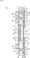
- FIG. 1 is a cross-sectional view showing a configuration example of a first embodiment of a semiconductor device to which the present technology is applied.
- the semiconductor device 1 of FIG. 1 has wiring layers 14A and 14B including one or more layers of wiring 12 and an insulating layer (interlayer insulating film) 13 on the lower surface and the upper surface of a glass substrate 11 to be a core substrate.
- the lower surface of the glass substrate 11 is the front surface of the glass substrate 11
- the upper surface of the glass substrate 11 is the back surface of the glass substrate 11.
- One or more through holes 15 are formed in a predetermined region of the glass substrate 11, and the wiring 12 of the wiring layer 14 A on the upper surface is formed by the through vias (through electrodes) 16 formed on the inner periphery of the through holes 15.
- the wiring 12 of the wiring layer 14B on the lower surface are electrically connected.
- the wiring layers 14A and 14B are also referred to as the wiring layer 14 when not particularly distinguished.
- the semiconductor device 1 further includes a cavity portion 17 in which the glass substrate 11 and the wiring layers 14A and 14B are opened at a substantially central portion in the plane direction.
- the electronic component 18 is disposed in the cavity portion 17, and the space other than the electronic component 18 in the cavity portion 17 is filled with the heat radiation conductive material 19 and the resin 20. More specifically, a plurality of through holes 19A penetrating the resin 20 filled above the electronic component 18 in the depth direction are formed, and the heat radiation conductive material 19 is embedded in each through hole 19A.
- the electronic component 18 is, for example, a component such as an antenna, a filter, a power amplifier, a switch, a low noise amplifier, a phase shifter, a mixer, a PLL, and a passive element.
- a heat spreader 31 is bonded to the upper surface of the wiring layer 14A on the upper side of the semiconductor device 1 with a thermally conductive adhesive 30 such as TIM (thermal interface material).
- a thermally conductive adhesive 30 such as TIM (thermal interface material).
- the rewiring 22 and the insulating layer 23 are formed on the lower surface of the wiring layer 14B under the semiconductor device 1, and the rewiring 22 is connected to the terminal 25 of the electronic component 18 through the via 24. It is connected or connected to the wiring 12 of the wiring layer 14B.
- the rewiring 22 electrically connects the terminal portion 25 of the electronic component 18 and the wiring 12 of the wiring layer 14B.
- the signal and power supply voltage supplied to the electronic component 18 are input from the external terminal 26 to the electronic component 18 through the rewiring 22, and the output signal of the electronic component 18 is output from the external terminal 26 through the rewiring 22. Be done.
- the external terminals 26 are, for example, solder bumps, and Ni / Au or Ni / Pd / Au plating (not shown) as UBM (Under Bump Metal) is formed on the surface of the rewiring 22 on which the external terminals 26 are disposed. It is formed.
- UBM Under Bump Metal
- the semiconductor device 1 can also be in a form in which the external terminal 26 is omitted.
- the rewiring 22 of the semiconductor device 1 and the main substrate are connected by solder bumps or the like.
- the heat radiation conductive material 19 is disposed in contact with the upper surface of the electronic component 18 disposed in the cavity portion 17, and the heat radiation conductive material 19 is formed of the heat conductive adhesive 30. It is connected with the heat sink 31 via the same.
- the heat radiation conductive material 19 By arranging the heat radiation conductive material 19 using a high thermal conductivity material in contact with the upper surface of the electronic component 18 instead of passing the heat radiation path of the electronic component 18 through the glass substrate 11 having low thermal conductivity, The heat dissipation efficiency can be improved.
- a heat dissipation structure with higher capacity can be realized by arranging the heat dissipation plate 31 on the upper surface of the semiconductor device 1 and connecting it to the heat dissipation conductive material 19 via the heat conductive adhesive 30. .
- the opening width of the wiring layer non-formed region 21 which is a region where the upper and lower wiring layers 14 of the glass substrate 11 are not formed is the glass opening which is the opening of the glass substrate 11.
- the width is wider than the width of the portion 32.
- the electronic component 18 having a different thermal expansion coefficient, the resin 20, and the wiring layer 14B are formed in divided regions in the planar direction.
- the stress between the resin 20 and the wiring layer 14B will be singular points. Stress is applied to the boundary 35 and the boundary 36 between the resin 20 and the electronic component 18 according to the thickness of the resin 20 due to expansion and contraction due to thermal cycle or the like, and the electronic component 18, resin 20, and It becomes a factor of the reliability fall of the rewiring 22 formed so as to straddle the wiring layer 14B.
- the end face of the glass substrate 11 is offset with respect to the end faces of the wiring layers 14A and 14B, and the boundary between the resin 20 and the wiring layer 14B.
- the stress applied to 35 is a stress corresponding to the thickness of the wiring layer 14A or 14B, so the stress load is reduced as compared with the case in A of FIG. Thereby, the reliability of the rewiring 22 formed over the entire lower surface can be improved.
- the wiring layer 14A and the wiring layer 14B are formed on the upper surface and the lower surface of the glass substrate 11, respectively.
- the wiring layer 14A and the wiring layer 14B are formed to secure the wiring layer non-formed region 21 having an opening width wider than the width of the glass opening 32 (FIG. 1).
- the glass substrate 11 on which the wiring layer 14A and the wiring layer 14B are formed is collectively referred to as a glass wiring substrate.
- non-alkali glass or low alkali glass which does not contain an alkali metal is desirable from the viewpoint of matching of the linear expansion coefficient with the incorporated electronic component 18 and wiring reliability.
- AN100 As a material of the glass substrate 11, AN100 (Asahi Glass Co., Ltd.), Eagle-XG (Corning), OA-10G (Nippon Electric Glass Co., Ltd.), or the like can be used.
- the wiring 12 in the wiring layer 14A and the wiring layer 14B can be formed by a semi-additive method using, for example, Cu as a metal material, but the material and formation method of the wiring 12 are not limited to this. The same applies to the material of the insulating layer 13. However, when the wiring layer non-formation region 21 is formed and the multilayer wiring 12 is required, the formation region of the wiring 12 and the wiring layer non-formation region 21 It is more preferable to use a thin film PID material (Photo Imageable Dielectric Material) as the material of the insulating layer 13 from the viewpoint of suppressing the step and suppressing the residue of the wiring layer non-formed region 21.
- a thin film PID material Photo Imageable Dielectric Material
- the resist 41 formed on the upper surfaces of the wiring layers 14A and 14B is, for example, an HF resistant resist corresponding to isotropic wet etching such as HF.
- the process of opening the glass substrate 11 is not particularly limited as long as it is a method such as laser ablation, stealth dicing, sand blasting, wet etching, etc. that can process glass materials at a practical speed.
- rough first processing and fine second processing such as a method of removing microcracks and residual stress layer on the end face after processing after opening by laser ablation processing by isotropic wet etching such as HF, etc.
- a method of processing in two stages can be adopted.
- a damage layer is formed to a depth of about 5 to 50 ⁇ m from the end face of the glass substrate 11, so from the end faces of the wiring layers 14A and 14B
- the amount of offset to the end face of the glass substrate 11 before the second processing is, for example, about 70 to 100 ⁇ m so as to be wider than the damaged layer.
- the opening of the glass substrate 11 may be performed by only one processing method such as only isotropic wet etching without performing processing in two steps.
- the glass opening 32 of the glass substrate 11 is formed wider than the unformed region 42 of the resist 41 by isotropic wet etching.
- the distance d1 in the planar direction from the end surface of the glass opening 32 to the end surface of the wiring layer 14 is shorter than the distance d2 in the planar direction from the end surface of the resist 41 to the end surface of the wiring layer 14.
- the resist 41 formed on the upper surface of the wiring layers 14A and 14B is removed. As a result, a cavity 17 in which the wiring layer non-formed region 21 and the glass opening 32 have an offset is formed.
- the support substrate 43 is temporarily bonded to the lower surface of the wiring layer 14B using a TB (Temporary-Bonding) material 44.
- a TB material 44 a material generally used in a Chip-first FO-WLP is used.
- the TB material 44 may be, for example, a thermal peeling type, an ultraviolet peeling type, or a chemical solution dissolving type.
- the support substrate 43 it is preferable to use the thing whose thermal expansion coefficient is the same as or close to the material used for a glass wiring board from a viewpoint of board
- the glass wiring substrate may be attached to the support substrate 43 first, and then the glass opening 32 may be formed. That is, the timing for forming the glass opening 32 may be before or after bonding the support substrate 43.
- the electronic component 18 is mounted face-down on the TB material 44 of the cavity portion 17.
- a chip mounter, flip chip bonder or the like can be used according to the type of electronic component 18, and the mounting accuracy is secured based on the alignment mark formed on the glass wiring substrate to improve the alignment accuracy. Then, the electronic component 18 can be arranged.
- the resin 20 is filled in a region other than the electronic component 18 of the cavity portion 17 formed on the glass wiring substrate.
- the filling method of the resin 20 is appropriately selected depending on the form and characteristics of the filling material. For example, vacuum lamination is used for film-shaped PID materials (polyimide, PBO, etc.) or ABF (Ajinomoto Build-up Film), vacuum screen printing for high viscosity resin, compression mold for mold compound, etc. It is selected. If the filled resin 20 remains on the back surface side of the glass wiring substrate by coating or lamination, it may be left as it is as a wiring insulating layer, or may be removed by polishing, surface planarization, etc. .
- the support substrate 43 is peeled off using a peeling method corresponding to the type of the TB material 44 used. At that time, if there is a residue on the terminal portion 25 of the electronic component 18 which is a peeling surface or on the surface of the connection pad of the wiring 12 on the lower surface of the glass substrate 11, desmear treatment such as plasma cleaning may be performed if necessary.
- the rewirings 22 and the insulating layer 23 are formed on the wiring layer 14B side of the glass wiring substrate.
- the wiring 12 and the rewiring 22 in the wiring layer 14B are electrically connected at predetermined positions by the vias 24.
- the rewirings 22 may be formed directly on the insulating layer 13 of the wiring layer 14B, but it is preferable to form the rewirings 22 after the insulating layer 23 is formed as in the present embodiment. It is.
- This is an electronic component as a step absorption layer when the rewiring 22 straddles between the electronic component 18, the resin 20, and the glass wiring substrate, and as a stress buffer layer at a connection portion with the electronic component 18. This is because the insulating layer 23 brings about the effect of suppressing ion migration along the 18 buried interfaces.
- through holes 19A are formed on the upper surface of the electronic component 18 in the cavity portion 17 filled with the resin 20, and the heat radiation conductive material 19 is embedded therein.
- an optimal method is selected according to the material of the resin 20. For example, if the material of the resin 20 is a PID material, the material of the resin 20 can be removed by exposure and development to form the through holes 19A.
- the through holes 19A may be opened by a CO 2 laser or the like and the heat radiation conductive material 19 may be embedded as shown in C of FIG. 5 similarly to the formation of TMV (Through Mold Via).
- TMV Through Mold Via
- Cu plating, an electrically conductive paste, etc. can be used for the thermal radiation conductive material 19
- metal materials with high thermal conductivity, such as Cu are more preferable.
- the heat radiation conductive material 19 may be embedded in the entire inside of the through hole 19A as shown in C of FIG.
- the inner peripheral surface of the through hole 19A and the upper surface of the metal layer 51 are embedded as shown in D of FIG.
- the entire inside of the through hole 19A may not be filled with the heat radiation conductive material 19.
- the planar shape of the through hole 19A may be circular or polygonal.
- the heat sink 31 is bonded to the upper surface of the wiring layer 14A using a thermally conductive adhesive 30 such as TIM.
- a thermally conductive adhesive 30 such as TIM.
- a conductive material such as a copper foil or a graphite sheet having high thermal conductivity in the planar direction is used.
- external terminals 26 such as solder bumps are formed on the lower surface of the wiring layer 14B on the lower side of the semiconductor device 1.
- FIG. 3 and FIG. 4 a portion corresponding to one semiconductor device 1 shown in FIG. 1 is illustrated, but a single large glass substrate such as that used in the manufacture of a liquid crystal panel is used as the glass substrate 11.
- a large number of semiconductor devices 1 can be manufactured simultaneously with the glass substrate 11 of FIG.
- the size of the glass substrate 11 may be a wafer size.
- the glass substrate 11 of the semiconductor device 1 functions as a reinforcing plate (stiffener) to suppress the warp of the semiconductor device 1 itself as a package as well as the warp of the panel during manufacture and the positional deviation of the electronic component 18 it can.
- the heat radiation path from the chip flip-chip connected to the glass wiring substrate is It is possible to either escape from the back side of the chip or to the back of the glass substrate through the flip chip connection portion and the glass penetrating electrode.
- the heat dissipation plate is disposed in the vicinity of the rewiring, and many of the heat dissipation plates are conductive materials, causing impedance deviation of the rewiring, which is particularly fatal to high frequency circuits. affect.
- the through vias 16 as fine wiring are formed in the glass wiring substrate, and the through holes for heat dissipation are formed in the resin 20 which is easier to process than the glass substrate 11. Through holes of optimum size can be formed.
- FIG. 6 is a cross-sectional view showing a first modification of the first embodiment.
- the heat radiation conductive material 71 in the form of a block (rectangular parallelepiped) is embedded in the resin 20 above the electronic component 18.
- the heat radiation conductive material 71 can be Cu plating, a conductive paste, etc. like the heat radiation conductive material 19, but a metal material having high thermal conductivity such as Cu is preferable.
- the structure of the heat radiation path formed of the heat radiation conductive material above the electronic component 18 is not limited to the through hole.
- the block-shaped heat-radiating conductive material 71 is attached to the upper surface (rear surface) in the process of mounting the electronic component 18 shown in FIG.
- the attached electronic component 18 may be mounted on the TB material 44.
- the height of the block-shaped heat radiation conductive material 71 is the same as the total height of the block-shaped heat radiation conductive material 71 and the electronic component 18 is the total height of the glass substrate 11 and the wiring layers 14A and 14B.
- the resin 20 is set, and the resin 20 is filled around the heat radiation conductive material 71 so as to form the same plane as the upper surface of the block shaped heat radiation conductive material 71.
- FIG. 7 is a cross-sectional view showing a second modification of the first embodiment.
- the 2nd modification of Drawing 7 shows an example of composition in case a plurality of thermal radiation conductive materials 19 formed above electronic parts 18 serve as a grand terminal.
- the rewiring 82 is formed on the top surface of the heat radiation conductive material 19 and the resin 20 of the cavity portion 17 and the wiring layer 14A via the insulating layer 81, and the rewiring 82 is formed with the plurality of heat radiation conductive materials 19 respectively. , Electrically connected by vias 83.
- the rewiring 82 is made of, for example, a metal material such as Cu, Al, W or the like.
- the rewiring 82 connected to the plurality of heat radiation conductive materials 19 is formed on the upper surface of the semiconductor device 1 as the heat sink 31 of FIG. 1, and the rewiring 82 has a function as the heat sink 31 of FIG. It can have a function as a ground terminal.
- FIG. 8 is a cross-sectional view showing a configuration example of a second embodiment of a semiconductor device to which the present technology is applied.
- the semiconductor device 1 according to the second embodiment of FIG. 8 is similar to the semiconductor device 1 of the second embodiment in that the heat dissipation plate 31 connected with the wiring layer 14A and the thermally conductive adhesive 30 is omitted on the upper surface of the glass substrate 11.
- the heat radiation conductive material 19 and the resin 20 are filled to a height reaching the wiring layer 14A formed on the upper surface of the glass substrate 11.
- the second embodiment of FIG. And the height to reach the upper surface (rear surface) of the glass substrate 11.
- the other configuration of the second embodiment is the same as that of the first embodiment.
- the wiring layer 14 formed in the semiconductor device 1 may be formed on only one of the upper surface and the lower surface of the glass substrate 11.
- the terminal portion 25 which is a signal input / output portion of the electronic component 18 or the semiconductor device 1.
- a wiring layer 14 is formed on the surface side of the glass substrate 11 on which the external terminal 26 which is a signal input / output unit is formed.
- the heat dissipation plate 31 is omitted together with the wiring layer 14 A on the upper surface of the glass substrate 11, but the heat dissipation plate 31 may be added in the form of being attached to the upper surface of the glass substrate 11 with the adhesive 30.
- the opening width of the wiring layer non-formed region 21 where the wiring layer 14B on the lower surface of the glass substrate 11 is not formed in the cavity 17 is larger than the width of the glass opening 32 of the glass substrate 11. It is widely open. Thus, as described with reference to FIG. 2, the reliability of the rewiring 22 formed on the entire lower surface can be improved.
- a plurality of through holes 19A are formed in a part of the resin 20 covering the electronic component 18, and the heat radiation conductive material 19 using a high thermal conductivity material is disposed from the upper surface of the electronic component 18 to the uppermost surface of the resin 20
- the heat dissipation efficiency can be improved.
- FIG. 9 is a cross-sectional view showing a configuration example of a third embodiment of a semiconductor device to which the present technology is applied.
- the heat sink 31 disposed on the top surface of the glass substrate 11 in the first embodiment is omitted.
- the heat sink 31 replaces with the heat sink 31, and discrete components 101, such as a chip capacitor, are mounted.
- the discrete component 101 is electrically connected to the wiring 12 of the wiring layer 14A at a predetermined location (not shown).
- the other configuration of the second embodiment is the same as that of the first embodiment.
- the discrete component 101 can be vertically stacked on the wiring layer 14A to reduce the footprint of the package.
- the opening width of the wiring layer non-formed area 21 where the wiring layer 14 is not formed with respect to the glass substrate 11 in the cavity 17 is larger than the width of the glass opening 32 of the glass substrate 11. It is widely open. Thus, as described with reference to FIG. 2, the reliability of the rewiring 22 formed on the entire lower surface can be improved.
- a plurality of through holes 19A are formed in a part of the resin 20 covering the electronic component 18, and the heat radiation conductive material 19 using a high thermal conductivity material is disposed from the upper surface of the electronic component 18 to the uppermost surface of the resin 20
- the heat dissipation efficiency can be improved.
- FIG. 10 is a cross-sectional view showing a configuration example of a fourth embodiment of a semiconductor device to which the present technology is applied.
- the semiconductor device 1 according to the fourth embodiment of FIG. 10 has a configuration in which the discrete component 101 in the third embodiment of FIG. 9 is replaced with the semiconductor element 102, and has a so-called PoP (Package on Package) structure. ing. Further, in the semiconductor device 1 of FIG. 10, as compared with the semiconductor device 1 of FIG. 9, the top and bottom of the glass wiring board are reversed, and the heat radiation path by the heat radiation conductive material 19 is downward. The external terminal 26 is connected to the wiring 12 of the wiring layer 14 A, and the semiconductor element 102 is connected to the rewiring 22 by the solder bump 103. The remaining structure of the fourth embodiment is similar to that of the first embodiment.
- miniaturization of the bump connection between the packages and high reliability can be realized by utilizing the fact that the thermal expansion coefficient of the glass substrate 11 matches with silicon. it can.
- the opening width of the wiring layer non-formed area 21 where the wiring layer 14 is not formed with respect to the glass substrate 11 in the cavity 17 is larger than the width of the glass opening 32 of the glass substrate 11. It is widely open. Thus, as described with reference to FIG. 2, the reliability of the rewiring 22 formed on the entire lower surface can be improved.
- a plurality of through holes 19A are formed in a part of the resin 20 covering the electronic component 18, and the heat radiation conductive material 19 using a high thermal conductivity material is disposed from the upper surface of the electronic component 18 to the uppermost surface of the resin 20
- the heat dissipation efficiency can be improved.
- the external terminal 26 may be omitted.
- FIGS. 11 and 12 show an example in which the semiconductor device 1 is configured as a functional module composed of a plurality of parts. Specifically, FIGS. 11 and 12 show an example in which the semiconductor device 1 is configured as a high frequency front end module.
- the semiconductor device 1 as the high frequency front end module of FIG. 11 includes a circuit block 121 and an antenna block 122.
- the wiring layers 14A and 14B are formed on the upper surface and the lower surface of the glass substrate 11, respectively, as in the first embodiment described above, and the cavity 17 is formed in a predetermined region of the glass substrate 11.
- One or more are provided, and the electronic component 18 is disposed in the cavity portion 17.
- the plurality of electronic components 18 in the circuit block 121 are, for example, power amplifiers.
- a heat radiation path is formed for each electronic component 18 by the heat radiation conductive material 19 and the heat radiation plate 31 disposed on the upper surface.
- the opening width of the wiring layer non-formation region 21 is wider than the width of the glass opening 32.
- the plurality of electronic components 18 in the circuit block 121 are connected by the rewiring 22 in the shortest path.
- an antenna circuit is configured by the wiring 12 of the wiring layer 14A formed on the upper surface of the glass substrate 11.
- a filter circuit, a passive element, or the like may be formed on the wiring layer 14A using the wiring 12.
- the antenna itself may vary in system depending on the mounted device. Therefore, as shown in FIG. 12, the antenna block 122 can be provided with the cavity portion 17 and the antenna chip 131 can be disposed in the cavity portion 17 similarly to the electronic component 18 of the circuit block 121. is there.
- 5G communication modules In recent years, the development of so-called 5G communication modules has been promoted by various companies due to demands for high-speed and large-capacity communication of portable devices in recent years, and high-speed communication functions with low delay accompanying edge computing.
- the signal frequency handled by this 5G front-end module is said to be around 30 GHz, and it is necessary to consider loss that can not be compared to the previous several GHz.
- the present technology it is possible to connect the electronic components 18 in the shortest and minimize the impedance deviation by using the high precision wiring 12 and the rewiring 22 on the glass substrate 11, and with the minimum loss.
- a high frequency front end module capable of transmitting and receiving signals can be realized. Furthermore, since the power amplifier used as the electronic component 18 in the high-frequency front end module generates a very large amount of heat, the formation of a heat radiation path is indispensable, and the heat radiation path by the heat radiation conductive material 19 and the heat radiation plate 31 is effective. Function.
- the technology according to the present disclosure can be applied to various products.
- the technology according to the present disclosure is any type of movement, such as automobiles, electric vehicles, hybrid electric vehicles, motorcycles, bicycles, personal mobility, airplanes, drones, ships, robots, construction machines, agricultural machines (tractors), etc. It may be realized as a device mounted on the body.
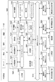
- FIG. 13 is a block diagram showing a schematic configuration example of a vehicle control system 7000 that is an example of a mobile control system to which the technology according to the present disclosure can be applied.
- Vehicle control system 7000 comprises a plurality of electronic control units connected via communication network 7010.
- the vehicle control system 7000 includes a drive system control unit 7100, a body system control unit 7200, a battery control unit 7300, an external information detection unit 7400, an in-vehicle information detection unit 7500, and an integrated control unit 7600. .
- the communication network 7010 connecting the plurality of control units is, for example, an arbitrary standard such as CAN (Controller Area Network), LIN (Local Interconnect Network), LAN (Local Area Network), or FlexRay (registered trademark). It may be an in-vehicle communication network.
- CAN Controller Area Network
- LIN Local Interconnect Network
- LAN Local Area Network
- FlexRay registered trademark
- Each control unit includes a microcomputer that performs arithmetic processing in accordance with various programs, a storage unit that stores programs executed by the microcomputer or parameters used in various arithmetic operations, and drive circuits that drive devices to be controlled. Equipped with Each control unit is provided with a network I / F for communicating with other control units via the communication network 7010, and by wired communication or wireless communication with an apparatus or sensor inside or outside the vehicle. A communication I / F for performing communication is provided. In FIG.
- a microcomputer 7610 for a functional configuration of the integrated control unit 7600, a microcomputer 7610, a general-purpose communication I / F 7620, a dedicated communication I / F 7630, a positioning unit 7640, a beacon receiving unit 7650, an in-vehicle device I / F 7660, an audio image output unit 7670, An in-vehicle network I / F 7680 and a storage unit 7690 are illustrated.
- the other control units also include a microcomputer, a communication I / F, a storage unit, and the like.
- Drive system control unit 7100 controls the operation of devices related to the drive system of the vehicle according to various programs.
- drive system control unit 7100 includes a drive force generation device for generating a drive force of a vehicle such as an internal combustion engine or a drive motor, a drive force transmission mechanism for transmitting the drive force to the wheels, and a steering angle of the vehicle. It functions as a control mechanism such as a steering mechanism that adjusts and a braking device that generates a braking force of the vehicle.
- the drive system control unit 7100 may have a function as a control device such as an ABS (Antilock Brake System) or an ESC (Electronic Stability Control).
- Vehicle state detection unit 7110 is connected to drive system control unit 7100.
- the vehicle state detection unit 7110 may be, for example, a gyro sensor that detects an angular velocity of an axial rotational movement of a vehicle body, an acceleration sensor that detects an acceleration of the vehicle, or an operation amount of an accelerator pedal, an operation amount of a brake pedal, and steering of a steering wheel. At least one of the sensors for detecting the angle, the engine speed, the rotational speed of the wheel, etc. is included.
- Drive system control unit 7100 performs arithmetic processing using a signal input from vehicle state detection unit 7110 to control an internal combustion engine, a drive motor, an electric power steering device, a brake device, and the like.
- Body system control unit 7200 controls the operation of various devices equipped on the vehicle body according to various programs.
- the body control unit 7200 functions as a keyless entry system, a smart key system, a power window device, or a control device of various lamps such as a head lamp, a back lamp, a brake lamp, a blinker or a fog lamp.
- the body system control unit 7200 may receive radio waves or signals of various switches transmitted from a portable device substituting a key.
- Body system control unit 7200 receives the input of these radio waves or signals, and controls a door lock device, a power window device, a lamp and the like of the vehicle.
- the battery control unit 7300 controls the secondary battery 7310 which is a power supply source of the drive motor according to various programs. For example, information such as the battery temperature, the battery output voltage, or the remaining capacity of the battery is input to the battery control unit 7300 from the battery device provided with the secondary battery 7310. The battery control unit 7300 performs arithmetic processing using these signals, and performs temperature adjustment control of the secondary battery 7310 or control of a cooling device or the like provided in the battery device.
- Outside-vehicle information detection unit 7400 detects information outside the vehicle equipped with vehicle control system 7000.
- the imaging unit 7410 and the external information detection unit 7420 is connected to the external information detection unit 7400.
- the imaging unit 7410 includes at least one of a time-of-flight (ToF) camera, a stereo camera, a monocular camera, an infrared camera, and another camera.
- ToF time-of-flight
- an environment sensor for detecting the current weather or weather, or another vehicle, an obstacle or a pedestrian around the vehicle equipped with the vehicle control system 7000 is detected in the outside-vehicle information detection unit 7420, for example.
- the ambient information detection sensors at least one of the ambient information detection sensors.
- the environment sensor may be, for example, at least one of a raindrop sensor that detects wet weather, a fog sensor that detects fog, a sunshine sensor that detects sunshine intensity, and a snow sensor that detects snowfall.
- the ambient information detection sensor may be at least one of an ultrasonic sensor, a radar device, and a light detection and ranging (LIDAR) device.
- the imaging unit 7410 and the external information detection unit 7420 may be provided as independent sensors or devices, or may be provided as an integrated device of a plurality of sensors or devices.
- FIG. 14 shows an example of installation positions of the imaging unit 7410 and the external information detection unit 7420.
- the imaging units 7910, 7912, 7914, 7916, 7918 are provided at, for example, at least one of the front nose of the vehicle 7900, the side mirror, the rear bumper, the back door, and the upper portion of the windshield of the vehicle interior.
- An imaging unit 7910 provided in the front nose and an imaging unit 7918 provided in the upper part of the windshield in the vehicle cabin mainly acquire an image in front of the vehicle 7900.
- the imaging units 7912 and 7914 provided in the side mirror mainly acquire an image of the side of the vehicle 7900.
- An imaging unit 7916 provided in the rear bumper or back door mainly acquires an image behind the vehicle 7900.
- the imaging unit 7918 provided on the upper part of the windshield in the passenger compartment is mainly used to detect a leading vehicle or a pedestrian, an obstacle, a traffic light, a traffic sign, a lane, or the like.
- FIG. 14 illustrates an example of the imaging range of each of the imaging units 7910, 7912, 7914, and 7916.
- the imaging range a indicates the imaging range of the imaging unit 7910 provided on the front nose
- the imaging ranges b and c indicate the imaging ranges of the imaging units 7912 and 7914 provided on the side mirrors
- the imaging range d indicates The imaging range of the imaging part 7916 provided in the rear bumper or the back door is shown.
- a bird's-eye view of the vehicle 7900 as viewed from above can be obtained.
- the external information detection units 7920, 7922, 7924, 7926, 7928, and 7930 provided on the front, rear, sides, and corners of the vehicle 7900 and above the windshield of the vehicle interior may be, for example, ultrasonic sensors or radar devices.
- the external information detection units 7920, 7926, 7930 provided on the front nose of the vehicle 7900, the rear bumper, the back door, and the upper part of the windshield of the vehicle interior may be, for example, a LIDAR device.
- These outside-of-vehicle information detection units 7920 to 7930 are mainly used for detecting a preceding vehicle, a pedestrian, an obstacle or the like.
- the out-of-vehicle information detection unit 7400 causes the imaging unit 7410 to capture an image outside the vehicle, and receives the captured image data. Further, the external information detection unit 7400 receives detection information from the external information detection unit 7420 connected. When the out-of-vehicle information detection unit 7420 is an ultrasonic sensor, a radar device, or a LIDAR device, the out-of-vehicle information detection unit 7400 transmits ultrasonic waves or electromagnetic waves and receives information on the received reflected waves.
- the external information detection unit 7400 may perform object detection processing or distance detection processing of a person, a car, an obstacle, a sign, a character on a road surface, or the like based on the received information.
- the external information detection unit 7400 may perform environment recognition processing for recognizing rainfall, fog, road surface conditions and the like based on the received information.
- the external information detection unit 7400 may calculate the distance to an object outside the vehicle based on the received information.
- the external information detection unit 7400 may perform image recognition processing or distance detection processing for recognizing a person, a car, an obstacle, a sign, a character on a road surface, or the like based on the received image data.
- the external information detection unit 7400 performs processing such as distortion correction or alignment on the received image data, and combines the image data captured by different imaging units 7410 to generate an overhead image or a panoramic image. It is also good.
- the external information detection unit 7400 may perform viewpoint conversion processing using image data captured by different imaging units 7410.
- An in-vehicle information detection unit 7500 detects information in the vehicle.
- a driver state detection unit 7510 that detects a state of a driver is connected to the in-vehicle information detection unit 7500.
- the driver state detection unit 7510 may include a camera for imaging the driver, a biometric sensor for detecting the driver's biological information, a microphone for collecting sound in the vehicle interior, and the like.
- the biological sensor is provided, for example, on a seat or a steering wheel, and detects biological information of an occupant sitting on a seat or a driver who grips the steering wheel.
- the in-vehicle information detection unit 7500 may calculate the degree of fatigue or concentration of the driver based on the detection information input from the driver state detection unit 7510, or determine whether the driver does not go to sleep You may The in-vehicle information detection unit 7500 may perform processing such as noise canceling processing on the collected audio signal.
- the integrated control unit 7600 controls the overall operation in the vehicle control system 7000 in accordance with various programs.
- An input unit 7800 is connected to the integrated control unit 7600.
- the input unit 7800 is realized by, for example, a device such as a touch panel, a button, a microphone, a switch or a lever, which can be input operated by the passenger.
- the integrated control unit 7600 may receive data obtained by speech recognition of speech input by the microphone.
- the input unit 7800 may be, for example, a remote control device using infrared rays or other radio waves, or an external connection device such as a mobile phone or a PDA (Personal Digital Assistant) corresponding to the operation of the vehicle control system 7000.
- PDA Personal Digital Assistant
- the input unit 7800 may be, for example, a camera, in which case the passenger can input information by gesture. Alternatively, data obtained by detecting the movement of the wearable device worn by the passenger may be input. Furthermore, the input unit 7800 may include, for example, an input control circuit that generates an input signal based on the information input by the passenger or the like using the above-described input unit 7800 and outputs the generated signal to the integrated control unit 7600. The passenger or the like operates the input unit 7800 to input various data to the vehicle control system 7000 and instruct processing operations.
- the storage unit 7690 may include a ROM (Read Only Memory) that stores various programs executed by the microcomputer, and a RAM (Random Access Memory) that stores various parameters, calculation results, sensor values, and the like.
- the storage unit 7690 may be realized by a magnetic storage device such as a hard disk drive (HDD), a semiconductor storage device, an optical storage device, a magneto-optical storage device, or the like.
- HDD hard disk drive
- semiconductor storage device an optical storage device
- magneto-optical storage device or the like.
- the general-purpose communication I / F 7620 is a general-purpose communication I / F that mediates communication with various devices existing in the external environment 7750.
- General-purpose communication I / F 7620 is a cellular communication protocol such as GSM (registered trademark) (Global System of Mobile communications), WiMAX (registered trademark), LTE (registered trademark) (Long Term Evolution) or LTE-A (LTE-Advanced).
- GSM Global System of Mobile communications
- WiMAX registered trademark
- LTE registered trademark
- LTE-A Long Term Evolution-Advanced
- other wireless communication protocols such as wireless LAN (also referred to as Wi-Fi (registered trademark)), Bluetooth (registered trademark), etc. may be implemented.
- the general-purpose communication I / F 7620 is connected to, for example, an apparatus (for example, an application server or control server) existing on an external network (for example, the Internet, a cloud network, or an operator-specific network) via a base station or access point
- an apparatus for example, an application server or control server
- an external network for example, the Internet, a cloud network, or an operator-specific network
- the general-purpose communication I / F 7620 is a terminal (for example, a driver, a pedestrian or a shop terminal, or an MTC (Machine Type Communication) terminal) existing near the vehicle using, for example, P2P (Peer To Peer) technology. It may be connected with
- the dedicated communication I / F 7630 is a communication I / F that supports a communication protocol designed for use in a vehicle.
- the dedicated communication I / F 7630 may be a standard protocol such as WAVE (Wireless Access in Vehicle Environment), DSRC (Dedicated Short Range Communications), or cellular communication protocol, which is a combination of lower layer IEEE 802.11p and upper layer IEEE 1609, for example. May be implemented.
- the dedicated communication I / F 7630 is typically used for Vehicle to Vehicle communication, Vehicle to Infrastructure communication, Vehicle to Home communication, and Vehicle to Pedestrian. 2.) Perform V2X communication, a concept that includes one or more of the communication.
- the positioning unit 7640 receives a GNSS signal (for example, a GPS signal from a Global Positioning System (GPS) satellite) from, for example, a Global Navigation Satellite System (GNSS) satellite and executes positioning, thereby performing latitude, longitude, and altitude of the vehicle.
- Generate location information including Positioning section 7640 may specify the current position by exchanging signals with the wireless access point, or may acquire position information from a terminal such as a mobile phone having a positioning function, a PHS, or a smartphone.
- the beacon receiving unit 7650 receives, for example, radio waves or electromagnetic waves transmitted from a radio station or the like installed on a road, and acquires information such as the current position, traffic jams, closing times or required time.
- the function of the beacon reception unit 7650 may be included in the above-described dedicated communication I / F 7630.
- An in-vehicle apparatus I / F 7660 is a communication interface that mediates the connection between the microcomputer 7610 and various in-vehicle apparatuses 7760 existing in the vehicle.
- the in-car device I / F 7660 may establish a wireless connection using a wireless communication protocol such as wireless LAN, Bluetooth (registered trademark), NFC (Near Field Communication), or WUSB (Wireless USB).
- a wireless communication protocol such as wireless LAN, Bluetooth (registered trademark), NFC (Near Field Communication), or WUSB (Wireless USB).
- the in-vehicle device I / F 7660 is connected via a connection terminal (not shown) (and, if necessary, a cable) via USB (Universal Serial Bus), HDMI (High-Definition Multimedia Interface), or MHL (Mobile)
- USB Universal Serial Bus
- HDMI High-Definition Multimedia Interface
- MHL Mobile
- the in-vehicle device 7760 may include, for example, at least one of a mobile device or wearable device owned by a passenger, or an information device carried in or attached to a vehicle. Further, the in-vehicle device 7760 may include a navigation device for performing a route search to any destination.
- the in-vehicle device I / F 7660 exchanges control signals or data signals with these in-vehicle devices 7760.
- the in-vehicle network I / F 7680 is an interface that mediates communication between the microcomputer 7610 and the communication network 7010.
- the in-vehicle network I / F 7680 transmits and receives signals and the like in accordance with a predetermined protocol supported by the communication network 7010.
- the microcomputer 7610 of the integrated control unit 7600 is connected via at least one of a general-purpose communication I / F 7620, a dedicated communication I / F 7630, a positioning unit 7640, a beacon reception unit 7650, an in-vehicle device I / F 7660, and an in-vehicle network I / F 7680.
- the vehicle control system 7000 is controlled in accordance with various programs based on the information acquired. For example, the microcomputer 7610 calculates a control target value of the driving force generation device, the steering mechanism or the braking device based on the acquired information inside and outside the vehicle, and outputs a control command to the driving system control unit 7100. It is also good.
- the microcomputer 7610 realizes the function of an advanced driver assistance system (ADAS) including collision avoidance or shock mitigation of a vehicle, follow-up traveling based on an inter-vehicle distance, vehicle speed maintenance traveling, vehicle collision warning, vehicle lane departure warning, etc. Cooperative control for the purpose of In addition, the microcomputer 7610 automatically runs without using the driver's operation by controlling the driving force generating device, the steering mechanism, the braking device, etc. based on the acquired information of the surroundings of the vehicle. Coordinated control may be performed for the purpose of driving and the like.
- ADAS advanced driver assistance system
- the microcomputer 7610 is information acquired via at least one of a general-purpose communication I / F 7620, a dedicated communication I / F 7630, a positioning unit 7640, a beacon reception unit 7650, an in-vehicle device I / F 7660, and an in-vehicle network I / F 7680. Based on the above, three-dimensional distance information between the vehicle and an object such as a surrounding structure or a person may be generated, and local map information including the peripheral information of the current position of the vehicle may be created. Further, the microcomputer 7610 may predict a danger such as a collision of a vehicle or a pedestrian or the like approaching a road or the like on the basis of the acquired information, and may generate a signal for warning.
- the warning signal may be, for example, a signal for generating a warning sound or lighting a warning lamp.
- the audio image output unit 7670 transmits an output signal of at least one of audio and image to an output device capable of visually or aurally notifying information to a passenger or the outside of a vehicle.
- an audio speaker 7710, a display unit 7720, and an instrument panel 7730 are illustrated as output devices.
- the display unit 7720 may include, for example, at least one of an on-board display and a head-up display.
- the display portion 7720 may have an AR (Augmented Reality) display function.
- the output device may be another device such as a headphone, a wearable device such as a glasses-type display worn by a passenger, a projector, or a lamp other than these devices.
- the display device may obtain information obtained from various processes performed by the microcomputer 7610 or information received from another control unit in various formats such as text, images, tables, graphs, etc. Display visually.
- the audio output device converts an audio signal composed of reproduced audio data or audio data into an analog signal and outputs it in an auditory manner.
- At least two control units connected via the communication network 7010 may be integrated as one control unit.
- each control unit may be configured by a plurality of control units.
- the vehicle control system 7000 may comprise another control unit not shown.
- part or all of the functions of any control unit may be provided to another control unit. That is, as long as transmission and reception of information are performed via the communication network 7010, predetermined arithmetic processing may be performed by any control unit.
- a sensor or device connected to any control unit is connected to another control unit, a plurality of control units may mutually transmit and receive detection information via the communication network 7010. .
- the semiconductor device 1 according to each embodiment described above can be applied to the integrated control unit 7600 of the application example shown in FIG.
- the configuration of the semiconductor device 1 shown in FIGS. 11 and 12 as at least one of the general-purpose communication I / F 7620, the dedicated communication I / F 7630, the beacon reception unit 7650, or the in-vehicle device I / F 7660 it can.
- 11 and 12 is adopted as a high frequency front end module included in the general-purpose communication I / F 7620, the dedicated communication I / F 7630, the beacon reception unit 7650, or the in-vehicle device I / F 7660
- the general-purpose communication I / F 7620 the dedicated communication I / F 7630
- the beacon reception unit 7650 the in-vehicle device I / F 7660
- the present technology can also have the following configurations.
- a semiconductor device comprising: rewiring for connecting the wiring of the glass substrate and the electronic component.
- the opening width of the wiring layer non-formed area which is the area where the wiring layer is not formed on the front surface or the back surface of the glass substrate is wider than the opening width of the opening formed in the glass substrate.
- the semiconductor device according to (1) (3) The semiconductor device according to (1) or (2), wherein a region other than the electronic component of the opening formed in the glass substrate is at least filled with a resin.
- the heat radiation conductive material is filled on the back surface side of the electronic component which is the opposite side to the surface on which the terminal portion connected to the rewiring is formed.
- the semiconductor device of description (5)
- the wiring layer is formed only on the surface of the glass substrate, The semiconductor device according to (4), wherein the heat radiation conductive material is configured to be filled to a height reaching the back surface of the glass substrate.
- the wiring layer is formed on front and back surfaces of the glass substrate, The semiconductor device according to (4), wherein the heat radiation conductive material is filled to a height reaching the wiring layer on the back surface of the glass substrate.
- the wiring layer is formed only on the surface side of the glass substrate, The semiconductor device according to any one of (1) to (11), further including discrete components on the back surface side of the glass substrate. (13) The wiring layer is formed on both the front and back surfaces of the glass substrate, The semiconductor device according to any one of (1) to (11), further including a semiconductor element on the wiring layer on the back surface side of the glass substrate. (14) Form a wiring layer including one or more layers of wiring on the surface or front and back of the glass substrate, Forming an opening in the glass substrate, and disposing an electronic component inside the opening; A rewiring for connecting the wiring of the glass substrate and the electronic component is formed.
- the back surface of the electronic component is filled with a resin, and further, a part of the resin is removed and the heat radiation conductive material is filled.
- the manufacturing method of the semiconductor device in any one of these.
- the electronic component having a block-shaped heat radiation conductive material attached to the back surface of the electronic component is disposed inside the opening, and the block-shaped heat radiation conductive material.
- Reference Signs List 1 semiconductor device 11 glass substrate, 3 pixel array portion, 12 wiring, 13 insulating layer, 14 (14A, 14B) wiring layer, 15 through hole, 16 through via, 17 cavity portion, 18 electronic parts, 19A through hole, 19 Heat radiation conductive material, 20 resin, 21 wiring layer non-formed area, 22 rewiring, 23 insulation layer, 25 terminal part, 26 external terminal, 31 heat sink, 32 glass opening, 42 unformed area, 71 heat conductive material, 82 Rewiring, 101 discrete components, 102 semiconductor devices
Landscapes
- Engineering & Computer Science (AREA)
- Manufacturing & Machinery (AREA)
- Microelectronics & Electronic Packaging (AREA)
- Production Of Multi-Layered Print Wiring Board (AREA)
- Physics & Mathematics (AREA)
- Geometry (AREA)
- Ceramic Engineering (AREA)
- Cooling Or The Like Of Semiconductors Or Solid State Devices (AREA)
- Internal Circuitry In Semiconductor Integrated Circuit Devices (AREA)
Abstract
本技術は、配線層を形成するガラス基板の信頼性を向上させることができるようにする半導体装置およびその製造方法に関する。 半導体装置は、表面または表裏面に1層以上の配線を含む配線層が形成されたガラス基板と、ガラス基板に形成されたガラス開口部の内側に配置された電子部品と、ガラス基板の配線と電子部品とを接続する再配線とを備える。本技術は、例えば、高周波フロントエンドモジュール等に適用できる。
Description
本技術は、半導体装置およびその製造方法に関し、特に、配線層を形成するガラス基板の信頼性を向上させることができるようにした半導体装置およびその製造方法に関する。
モバイル機器に代表される近年の電子機器では、機器内に搭載される電子部品の継続的な小型・薄型化要求に加え、使用される素子の高性能化、多機能化、通信速度・容量の増大に伴う信号周波数の上昇などにも対応することが求められている。
これらの要求に応えるため、様々な実装・パッケージング技術が進展している。その中でも注目すべき技術に、例えば、非特許文献1に開示されるような、FO-WLP(Fan-out Wafer Level Package)がある。これは、ベアチップ上に形成された再配線(RDL: Redistribution Layer)がチップ外形より外側に拡張された、いわゆるFan-out型パッケージの一種である。FO-WLPは、従来のウェハプロセスで用いられる薄膜配線プロセスを、再配線工程に適用することで、微細化を実現している。FO-WLPによって、複数のチップ間を高密度な配線で接続したマルチチップモジュールの実現や、従来パッケージからの大幅な小型・薄型化が期待される。
FO-WLPの形成方法には、非特許文献1に開示された、ベアチップをモールド樹脂に埋め込んだ疑似ウェハを形成し、そこに再配線を形成する、Chip-first方式と、先に形成した再配線上にベアチップをフリップチップ実装する、いわゆるRDL-first方式とがあるが、Chip-first方式が主流である。特に、高速かつ高周波の信号を扱うパッケージでは、Chip-first方式の、ベアチップと再配線の接続部にバンプやワイヤを介さない構造が、接続部の寄生インダクタンスや信号のリターンロスの抑制に有効である。
しかし、このChip-first方式では、ベアチップが良品であっても、再配線の部分に不良個所があると、パッケージとしては不良となってしまう。再配線の形成不良の原因の一つとして、モールド樹脂で形成した疑似ウェハの反りや、モールド硬化時の収縮によるベアチップ位置ずれが挙げられる。特に複数のベアチップを接続するマルチチップモジュールでは、ウェハ内での位置ずれに加え、パッケージ領域内でのチップ間の位置ずれも複合的に発生する。
このような状況に対し、パッケージの剛性を維持する絶縁基材に少なくとも1層の配線を形成し、その後、配線を形成した絶縁基材に貫通孔を開口してベアチップを埋め込んでから、再配線を形成する、いわばChip-middle方式ともいうべき技術が提案されている(特許文献1参照)。
M. Brunnbauer et al. ,"Embedded wafer level ball grid array (eWLB)", 2006, EPTC '06. 8th
特許文献1では、パッケージの剛性を維持する絶縁基材の例として、熱硬化性樹脂、熱可塑性樹脂、ガラス、セラミック、プラスチックなどが開示されているが、絶縁基材としてガラスを用いる場合には、脆性材料であるガラスに貫通孔を開口する際に、ダメージが発生しやすかった。
本技術は、このような状況に鑑みてなされたものであり、配線層を形成するガラス基板の信頼性を向上させることができるようにするものである。
本技術の第1の側面の半導体装置は、表面または表裏面に1層以上の配線を含む配線層が形成されたガラス基板と、前記ガラス基板に形成された開口部の内側に配置された電子部品と、前記ガラス基板の前記配線と前記電子部品とを接続する再配線とを備える。
本技術の第1の側面においては、表面または表裏面に1層以上の配線を含む配線層が形成されたガラス基板と、前記ガラス基板に形成された開口部の内側に配置された電子部品と、前記ガラス基板の前記配線と前記電子部品とを接続する再配線とが設けられる。
本技術の第2の側面の半導体装置の製造方法は、ガラス基板の表面または表裏面に、1層以上の配線を含む配線層を形成し、前記ガラス基板に開口部を形成して、前記開口部の内側に電子部品を配置し、前記ガラス基板の前記配線と前記電子部品とを接続する再配線を形成する。
本技術の第2の側面においては、ガラス基板の表面または表裏面に、1層以上の配線を含む配線層が形成され、前記ガラス基板に開口部が形成されて、前記開口部の内側に電子部品が配置され、前記ガラス基板の前記配線と前記電子部品とを接続する再配線が形成される。
半導体装置は、独立した装置であっても良いし、他の装置に組み込まれるモジュールであっても良い。
本技術の第1および第2の側面によれば、配線層を形成するガラス基板の信頼性を向上させることができる。
なお、ここに記載された効果は必ずしも限定されるものではなく、本開示中に記載されたいずれかの効果であってもよい。
以下、本技術を実施するための形態(以下、実施の形態という)について説明する。なお、説明は以下の順序で行う。
1.半導体装置の第1の実施の形態
1.1 半導体装置の断面図
1.2 半導体装置の製造方法
2.第1実施の形態の変形例
2.1 第1変形例
2.2 第2変形例
3.半導体装置の第2の実施の形態
4.半導体装置の第3の実施の形態
5.半導体装置の第4の実施の形態
6.半導体装置の第5及び第6実施の形態
7.応用例
1.半導体装置の第1の実施の形態
1.1 半導体装置の断面図
1.2 半導体装置の製造方法
2.第1実施の形態の変形例
2.1 第1変形例
2.2 第2変形例
3.半導体装置の第2の実施の形態
4.半導体装置の第3の実施の形態
5.半導体装置の第4の実施の形態
6.半導体装置の第5及び第6実施の形態
7.応用例
<1.半導体装置の第1の実施の形態>
<1.1 半導体装置の断面図>
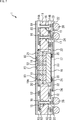
図1は、本技術を適用した半導体装置の第1実施の形態の構成例を示す断面図である。
<1.1 半導体装置の断面図>
図1は、本技術を適用した半導体装置の第1実施の形態の構成例を示す断面図である。
図1の半導体装置1は、コア基板となるガラス基板11の下面及び上面のそれぞれに、1層以上の配線12と絶縁層(層間絶縁膜)13とを含む配線層14Aおよび14Bを有する。図1において、ガラス基板11の下面がガラス基板11の表面であり、ガラス基板11の上面がガラス基板11の裏面である。ガラス基板11の所定の領域には、貫通孔15が1つ以上形成されており、貫通孔15の内周に形成された貫通ビア(貫通電極)16によって、上面の配線層14Aの配線12と、下面の配線層14Bの配線12とが電気的に接続されている。以下において、配線層14Aおよび14Bを特に区別しない場合には、配線層14とも称する。
また、半導体装置1は、平面方向略中央部において、ガラス基板11および配線層14Aおよび14Bが開口されたキャビティ部17を装置内に備える。キャビティ部17には、電子部品18が配置され、キャビティ部17内の電子部品18以外の空間には、放熱伝導材19および樹脂20が充填されている。より具体的には、電子部品18上方に充填された樹脂20を深さ方向に貫通する貫通孔19Aが複数形成され、各貫通孔19Aの内部に、放熱伝導材19が埋め込まれている。電子部品18は、例えば、アンテナ、フィルタ、パワーアンプ、スイッチ、低ノイズアンプ、フェーズシフタ、ミキサ、PLL、受動素子などの部品である。
半導体装置1の上側となる配線層14Aの上面には、TIM(thermal interface material)等の熱伝導性の接着剤30により、放熱板(ヒートスプレッダー)31が接着されている。これにより、放熱伝導材19によって電子部品18の上側に逃がした熱を拡散して、放熱させることができる。
一方、半導体装置1の下側となる配線層14Bの下面には、再配線22および絶縁層23が形成されており、再配線22は、ビア24を介して、電子部品18の端子部25と接続されたり、配線層14Bの配線12と接続されている。再配線22は、電子部品18の端子部25と、配線層14Bの配線12とを電気的に接続する。電子部品18に供給される信号や電源電圧は、外部端子26から再配線22を介して電子部品18に入力されるとともに、電子部品18の出力信号が再配線22を介して外部端子26から出力される。外部端子26は、例えば、はんだバンプであり、外部端子26が配置される再配線22の表面には、UBM(Under Bump Metal)としてのNi/AuまたはNi/Pd/Auメッキ(不図示)が形成されている。
なお、半導体装置1は、外部端子26を省略した形態とすることもできる。この場合、例えば、半導体装置1を主基板にマウントする際に、半導体装置1の再配線22と主基板が、はんだバンプ等により接続される。
以上のように構成される半導体装置1において、キャビティ部17に配置された電子部品18の上面と接する形で放熱伝導材19が配置され、放熱伝導材19は、熱伝導性の接着剤30を介して、放熱板31と接続されている。
電子部品18の放熱パスを、熱伝導性の低いガラス基板11を経由するのではなく、高熱伝導率材料を用いた放熱伝導材19を、電子部品18の上面と接する形で配置することで、放熱効率を向上させることができる。また、半導体装置1の上面に放熱板31を配置し、熱伝導性の接着剤30を介して放熱伝導材19と接続する構造とすることで、より高い容量の放熱構造を実現することができる。
また、半導体装置1では、キャビティ部17において、ガラス基板11の上下の配線層14が形成されていない領域である配線層未形成領域21の開口幅が、ガラス基板11の開口部であるガラス開口部32の幅よりも広く構成されている。
半導体装置1においては、再配線22を含む絶縁層23の上に、熱膨張係数の異なる電子部品18、樹脂20、および、配線層14Bが、平面方向に領域を分けて形成されている。
仮に、図2のAに示されるように、配線層14Aおよび14Bの端面と、ガラス基板11の端面が同一平面となっていた場合、応力の特異点となる、樹脂20と配線層14Bとの境界35、および、樹脂20と電子部品18との境界36には、サーマルサイクル(Thermal Cycle)などによる伸縮により、樹脂20の厚みに応じた応力負荷がかかり、電子部品18、樹脂20、および、配線層14Bを跨るように形成された再配線22の信頼性低下の要因となる。
これに対して、半導体装置1では、図2のBに示されるように、ガラス基板11の端面が配線層14Aおよび14Bの端面に対してオフセットされており、樹脂20と配線層14Bとの境界35にかかる応力は、配線層14Aまたは14Bの厚みに応じた応力となるので、図2のAにおける場合と比較して、応力負荷が軽減される。これにより、下面全面にわたって形成された再配線22の信頼性を向上させることができる。
<1.2 半導体装置の製造方法>
次に、図3および図4を参照して、図1に示した半導体装置1の製造方法について説明する。
次に、図3および図4を参照して、図1に示した半導体装置1の製造方法について説明する。
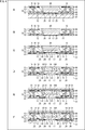
初めに、図3のAに示されるように、ガラス基板11の上面及び下面に、配線層14Aおよび配線層14Bが形成される。配線層14Aおよび配線層14Bは、ガラス開口部32(図1)の幅よりも広い開口幅の配線層未形成領域21を確保して形成される。以下の説明では、配線層14Aおよび配線層14Bが形成されたガラス基板11を、まとめて、ガラス配線基板とも称する。
ガラス基板11の材料としては、内蔵される電子部品18との線膨張係数の整合、および、配線信頼性の観点から、アルカリ金属を含まない無アルカリガラスまたは低アルカリガラスが望ましい。例えば、ガラス基板11の材料には、AN100(旭硝子株式会社)、Eagle-XG(コーニング社)、OA-10G(日本電気硝子株式会社)、などを用いることができる。
配線層14Aおよび配線層14B内の配線12は、例えば、金属材料としてCuを用いて、セミアディティブ法により形成することができるが、配線12の材料および形成方法は、これに限定されない。絶縁層13の材料についても同様のことが言えるが、配線層未形成領域21を形成し、かつ多層の配線12が必要な場合には、配線12の形成領域と配線層未形成領域21との段差を抑え、かつ配線層未形成領域21の残渣抑制の観点から、絶縁層13の材料として、薄膜のPID材料(Photo Imageable Dielectric Material)を用いるのが、より好適である。
次に、図3のBに示されるように、ガラス基板11の上面及び下面に形成された配線層14Aおよび配線層14Bを覆うようにレジスト41を形成した後、レジスト41が形成されていない領域のガラス基板11が除去される。これにより、図3のCに示されるように、ガラス基板11が開口される。配線層14Aおよび14B上面に形成されるレジスト41は、例えば、HF等の等方性ウェットエッチングに対応した耐HFレジストなどされる。
ガラス基板11を開口するプロセスは、レーザによるアブレーションやステルスダイシング、サンドブラスト、ウェットエッチング、等、ガラス材料を実用的な速度で加工できる方法であれば、特に限定されない。例えば、レーザアブレーション加工により開口した後、加工後の端面のマイクロクラックや残留応力層をHF等の等方性ウェットエッチングで除去する方法など、粗めの第1の加工と微細な第2の加工の2段階で加工する方法を採用することができる。この場合、加工方法によっても異なるが、粗めの第1の加工において、ガラス基板11の端面から5乃至50um程度の深さにダメージ層が形成されるので、配線層14Aおよび14Bの端面から、第2の加工前のガラス基板11の端面までのオフセット量が、そのダメージ層よりも広い幅となるように、例えば、70乃至100um程度とされる。なお、ガラス基板11の開口は、2段階による加工を行わずに、等方性ウェットエッチングのみ、など、1つの加工方法のみで行ってもよい。ガラス基板11のガラス開口部32は、等方性ウェットエッチングにより、レジスト41の未形成領域42よりも広く形成される。その結果、ガラス開口部32の端面から配線層14の端面までの平面方向の距離d1は、レジスト41の端面から配線層14の端面までの平面方向の距離d2よりも短くなる。
ガラス基板11にガラス開口部32が形成された後、図3のDに示されるように、配線層14Aおよび14B上面に形成されたレジスト41が除去される。これにより、配線層未形成領域21とガラス開口部32がオフセットを有するキャビティ部17が形成される。
続いて、図3のEに示されるように、支持基板43が、TB(Temporary-Bonding)材44を用いて、配線層14Bの下面に仮接合される。TB材44には、Chip-first方式のFO-WLPで一般的に用いられる材料が用いられる。TB材44には、例えば、熱剥離タイプ、紫外線剥離タイプ、薬液溶解タイプ等がある。また、支持基板43は、貼り付け後の基板反り抑制の観点から、熱膨張係数が、ガラス配線基板に用いる材料と同一または近いものを用いることが望ましい。なお、ガラス配線基板に対するガラス開口部32の開口面積比率が高い場合は、ガラス開口部32を形成した後のガラス配線基板の剛性が低下して破損しやすくなる。そのため、先に支持基板43をガラス配線基板を貼り付け、その後で、ガラス開口部32を形成してもよい。すなわち、ガラス開口部32を形成するタイミングは、支持基板43を貼り合わせる前でも後でも良い。
次に、図3のFに示されるように、キャビティ部17のTB材44上に、電子部品18が、Face-downでマウントされる。マウントには、電子部品18の種類に応じて、チップマウンターやフリップチップボンダーなどを用いることができ、アライメント精度向上のため、ガラス配線基板に形成しておいたアライメントマークを基準に搭載精度を確保して、電子部品18を配置することが可能である。
次に、図4のAに示されるように、ガラス配線基板に形成されたキャビティ部17の電子部品18以外の領域に、樹脂20が充填される。樹脂20の充填方法は、充填材料の形態や特性によって、適切に選択される。例えば、フィルム形状のPID材料(ポリイミド、PBO、等)やABF(Ajinomoto Build-up Film)であれば真空ラミネート、高粘度の樹脂であれば真空スクリーン印刷、モールドコンパウンドであればコンプレッションモールド、等が選択される。なお、塗布やラミネートによって、充填した樹脂20がガラス配線基板の裏面側に残存する場合は、そのまま残して配線絶縁層としてもよいし、研磨、サーフェスプレーナー等による除去および平坦化を行ってもよい。
次に、図4のBに示されるように、使用したTB材44の種類に応じた剥離方法を用いて、支持基板43が剥離される。その際、剥離面である電子部品18の端子部25やガラス基板11の下面の配線12の接続パッド表面に残渣がある場合は、必要に応じてプラズマクリーニングなどのデスミア処理を行ってもよい。
次に、図4のCに示されるように、ガラス配線基板の配線層14B側に、再配線22および絶縁層23が形成される。配線層14B内の配線12と再配線22は、ビア24により所定の箇所で電気的に接続される。配線層14Bの絶縁層13の上に、直接、再配線22を形成してもよいが、本実施の形態のように、絶縁層23を形成してから、再配線22を形成する方が好適である。これは、電子部品18、樹脂20、および、ガラス配線基板の間を再配線22がまたぐ際の段差吸収層として、また、電子部品18との接続部の応力バッファ層として、さらには、電子部品18の埋め込み界面に沿ったイオンマイグレーションの抑制として、の効果を絶縁層23がもたらすためである。
次に、図4のDに示されるように、樹脂20を充填したキャビティ部17内の電子部品18上面に、貫通孔19Aを形成し、その内部に放熱伝導材19が埋め込まれる。
放熱伝導材19を埋め込む貫通孔19Aの形成方法としては、樹脂20の材料に応じて最適な手法が選択される。例えば、樹脂20の材料が、PID材料であれば、露光および現像によって樹脂20の材料を除去して貫通孔19Aを形成することができる。
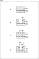
また例えば、樹脂20の材料が、モールド樹脂等であれば、図5のAに示されるように、電子部品18の上面に、メタル層51を予め形成しておき、これをストッパーとして、図5のBに示されるように、TMV(Through Mold Via)の形成と同様に、CO2レーザ等で貫通孔19Aを開口し、図5のCに示されるように、放熱伝導材19を埋め込めばよい。放熱伝導材19には、Cuめっき、導電性ペーストなどとすることができるが、Cuなどの高熱伝導率を持つ金属材料が、より好適である。放熱伝導材19は、図5のCのように、貫通孔19Aの内部全体に埋め込んでもよいが、図5のDのように、貫通孔19Aの内周面と、メタル層51の上面を埋め込む形として、貫通孔19A内部全体が放熱伝導材19で埋められなくてもよい。また、貫通孔19Aの平面形状は、円形でも多角形でもよい。
次に、図4のEに示されるように、配線層14Aの上面に、TIM等の熱伝導性の接着剤30を用いて、放熱板31が接着される。放熱板31には、例えば、銅箔やグラファイトシート等、平面方向に高い熱伝導率を持つ導電性材料が用いられる。
最後に、図4のFに示されるように、半導体装置1下側の配線層14Bの下面に、はんだバンプ等の外部端子26が形成される。
以上で、図1の半導体装置1が完成する。
図3および図4では、図1に示した1個の半導体装置1に相当する部分を図示したが、ガラス基板11として、液晶パネルの製造で用いられるような大型ガラス基板を用いて、1枚のガラス基板11で、多数の半導体装置1を同時に製造することが可能である。また、ガラス基板11のサイズは、ウエハサイズであってもよい。
半導体装置1のガラス基板11は、補強板(スティフナ)として機能し、パッケージとしての半導体装置1自体の反りは勿論、製造時のパネルの反りと、電子部品18の位置ずれをも抑制することができる。
先に形成した再配線上にベアチップ(電子部品18)をフリップチップ実装する、いわゆるRDL-first方式によるFO-WLP構造では、ガラス配線基板に対してフリップチップ接続されているチップからの放熱パスは、チップ裏面側から逃がすか、フリップチップ接続部とガラス貫通電極を介してガラス基板裏面に逃がすか、のいずれかが考えられる。
チップ裏面側から逃がす方式では、再配線近傍に放熱板を配置することになり、放熱板の多くは導電性材料であるため、再配線のインピーダンスずれを引き起こし、特に高周波回路に対して致命的な影響を及ぼす。
一方、フリップチップ接続部とガラス貫通電極を介してガラス基板裏面に逃がす方式では、ガラス貫通電極の熱抵抗を下げようとすると、ガラス貫通孔の径が大きくなり微細化に不利となり、径が小さいままでは熱抵抗が高くなる。また、径の異なる貫通孔を同時に開口するガラス加工技術は、実用的にはまだ存在しない。
図1の半導体装置1の構造によれば、微細配線としての貫通ビア16についてはガラス配線基板に形成し、放熱のための貫通孔はガラス基板11より加工しやすい樹脂20に形成するため、それぞれ最適なサイズの貫通孔を形成することができる。
<2.第1実施の形態の変形例>
<2.1 第1変形例>
図6は、第1実施の形態の第1変形例を示す断面図である。
<2.1 第1変形例>
図6は、第1実施の形態の第1変形例を示す断面図である。
図6以降に示す変形例およびその他の実施の形態おいては、図1で示した第1実施の形態と対応する部分については同一の符号を付してあり、その部分の説明は適宜省略する。
図1で示した第1実施の形態では、電子部品18上方の樹脂20に複数の貫通孔19Aが形成され、各貫通孔19Aの内部に、放熱伝導材19が埋め込まれていた。
これに対して、図6の第1変形例では、電子部品18上方の樹脂20内に、ブロック(直方体)形状の放熱伝導材71が埋め込まれている。放熱伝導材71は、放熱伝導材19と同様、Cuめっき、導電性ペーストなどとすることができるが、Cuなどの高熱伝導率を持つ金属材料が好適である。このように、電子部品18上方に放熱伝導材で形成される放熱パスの構造は、貫通孔に限られない。
なお、図6に示したようなブロック形状の放熱伝導材71とする場合、図3のFで示した電子部品18をマウントする工程において、ブロック形状の放熱伝導材71が上面(裏面)に貼り付けられた電子部品18を、TB材44上にマウントすればよい。ブロック形状の放熱伝導材71と電子部品18を合わせた高さが、ガラス基板11と配線層14Aおよび14Bとを合わせた高さと同じになるように、ブロック形状の放熱伝導材71の高さが設定され、樹脂20が、ブロック形状の放熱伝導材71の上面と同一平面を形成するように、放熱伝導材71の周囲に充填される。
<2.2 第2変形例>
図7は、第1実施の形態の第2変形例を示す断面図である。
図7は、第1実施の形態の第2変形例を示す断面図である。
図7の第2変形例は、電子部品18上方に形成された複数の放熱伝導材19が、グランド端子を兼ねる場合の構成例を示している。
具体的には、キャビティ部17の放熱伝導材19および樹脂20と配線層14Aの上面に、絶縁層81を介して再配線82が形成され、再配線82は、複数の放熱伝導材19それぞれと、ビア83で電気的に接続されている。再配線82は、例えば、Cu,Al,Wなどの金属材料で構成される。
このように、図1の放熱板31として、複数の放熱伝導材19と接続する再配線82を半導体装置1の上面に形成し、再配線82に、図1の放熱板31としての機能と、グランド端子としての機能を持たせることができる。
<3.半導体装置の第2の実施の形態>
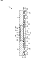
図8は、本技術を適用した半導体装置の第2実施の形態の構成例を示す断面図である。
図8は、本技術を適用した半導体装置の第2実施の形態の構成例を示す断面図である。
図8の第2実施の形態に係る半導体装置1は、ガラス基板11の上面に、配線層14Aと、熱伝導性の接着剤30で接続された放熱板31が省略されている点で、図1で示した第1実施の形態に係る半導体装置1と異なる。図1の第1実施の形態では、放熱伝導材19および樹脂20が、ガラス基板11上面に形成された配線層14Aに到達する高さまで充填されていたが、図8の第2実施の形態では、ガラス基板11の上面(裏面)に到達する高さまで充填されている。第2実施の形態のその他の構成は、第1実施の形態と同様である。
このように、半導体装置1に形成される配線層14は、ガラス基板11の上面または下面のいずれか一方のみに形成されてもよい。配線層14が、ガラス基板11の上面または下面のいずれか一方のみに形成される場合、図8に示されるように、電子部品18の信号入出力部である端子部25や、半導体装置1の信号入出力部である外部端子26が形成された、ガラス基板11の表面側に、配線層14が形成される。
図8の例では、ガラス基板11の上面の配線層14Aとともに、放熱板31も省略したが、放熱板31は、ガラス基板11上面に接着剤30で貼り付ける形で追加してもよい。
第2実施の形態においても、キャビティ部17において、ガラス基板11の下面の配線層14Bが形成されていない配線層未形成領域21の開口幅は、ガラス基板11のガラス開口部32の幅よりも広く開口されている。これにより、図2を参照して説明したように、下面全面に形成された再配線22の信頼性を向上させることができる。
また、電子部品18を覆う樹脂20の一部に複数の貫通孔19Aを形成し、高熱伝導率材料を用いた放熱伝導材19を、電子部品18の上面から樹脂20の最上面まで配置したことで、放熱効率を向上させることができる。
<4.半導体装置の第3の実施の形態>
図9は、本技術を適用した半導体装置の第3実施の形態の構成例を示す断面図である。
図9は、本技術を適用した半導体装置の第3実施の形態の構成例を示す断面図である。
図9の第3実施の形態に係る半導体装置1を、図1の第1実施の形態と比較すると、第1実施の形態においてガラス基板11上面に配置されていた放熱板31が省略されている。そして、放熱板31に代えて、チップコンデンサ等のディスクリート部品101が搭載されている。ディスクリート部品101は、図示せぬ所定の箇所において、配線層14Aの配線12と電気的に接続されている。第2実施の形態のその他の構成は、第1実施の形態と同様である。
ガラス基板11上面に形成された配線層14Aを使って、抵抗やインダクタ等のIPD(Integrated Passive Device)をガラス配線基板に組み込むことも可能であるが、それでは足りない、またはフットプリントが大きくなりすぎる素子については、第3実施の形態のように、ディスクリート部品101を配線層14A上に縦積みにして、パッケージのフットプリントを縮小することができる。
第3実施の形態においても、キャビティ部17において、ガラス基板11に対して配線層14が形成されていない配線層未形成領域21の開口幅は、ガラス基板11のガラス開口部32の幅よりも広く開口されている。これにより、図2を参照して説明したように、下面全面に形成された再配線22の信頼性を向上させることができる。
また、電子部品18を覆う樹脂20の一部に複数の貫通孔19Aを形成し、高熱伝導率材料を用いた放熱伝導材19を、電子部品18の上面から樹脂20の最上面まで配置したことで、放熱効率を向上させることができる。
<5.半導体装置の第4の実施の形態>
図10は、本技術を適用した半導体装置の第4実施の形態の構成例を示す断面図である。
図10は、本技術を適用した半導体装置の第4実施の形態の構成例を示す断面図である。
図10の第4実施の形態に係る半導体装置1は、図9の第3実施の形態におけるディスクリート部品101が、半導体素子102に置き換えられた構成であり、いわゆるPoP(Package on Package)構造となっている。また、図10の半導体装置1は、図9の半導体装置1と比較すると、ガラス配線基板の上下が反転されており、放熱伝導材19による放熱パスが下向きとなっている。外部端子26は、配線層14Aの配線12と接続されており、半導体素子102は、再配線22と、はんだバンプ103によって接続されている。第4実施の形態のその他の構成は、第1実施の形態と同様である。
第4実施の形態の半導体装置1によれば、ガラス基板11の熱膨張係数が、シリコンと整合していることを活かして、パッケージ間のバンプ接続の微細化と高信頼性を実現することができる。
第4実施の形態においても、キャビティ部17において、ガラス基板11に対して配線層14が形成されていない配線層未形成領域21の開口幅は、ガラス基板11のガラス開口部32の幅よりも広く開口されている。これにより、図2を参照して説明したように、下面全面に形成された再配線22の信頼性を向上させることができる。
また、電子部品18を覆う樹脂20の一部に複数の貫通孔19Aを形成し、高熱伝導率材料を用いた放熱伝導材19を、電子部品18の上面から樹脂20の最上面まで配置したことで、放熱効率を向上させることができる。
なお、図8乃至図10に示した第2乃至第4実施の形態においても、外部端子26を省略した形態をとり得る。
<6.半導体装置の第5及び第6実施の形態>
図11および図12は、本技術を適用した半導体装置の第5及び第6実施の形態の構成例を示す断面図である。
図11および図12は、本技術を適用した半導体装置の第5及び第6実施の形態の構成例を示す断面図である。
図11および図12は、半導体装置1を、複数の部品から成る機能モジュールとして構成した例である。具体的には、図11および図12は、半導体装置1を高周波フロントエンドモジュールとして構成した例を示している。
図11の高周波フロントエンドモジュールとしての半導体装置1は、回路ブロック121とアンテナブロック122を備える。
回路ブロック121には、上述した第1実施の形態と同様に、ガラス基板11の上面及び下面のそれぞれに配線層14Aおよび14Bが形成されるとともに、ガラス基板11の所定の領域に、キャビティ部17が1つ以上設けられ、キャビティ部17内に電子部品18が配置されている。回路ブロック121内の複数の電子部品18は、例えば、パワーアンプなどである。各電子部品18に対しては、上面に配置された放熱伝導材19および放熱板31により放熱パスが形成されている。また、各キャビティ部17において、配線層未形成領域21の開口幅が、ガラス開口部32の幅よりも広く開口されている。回路ブロック121内の複数の電子部品18は、再配線22により最短経路で接続されている。
一方、アンテナブロック122では、ガラス基板11の上面に形成された配線層14Aの配線12によって、アンテナ回路が構成されている。配線層14Aには、アンテナ回路以外に、フィルタ回路、受動素子などを、配線12を用いて形成してもよい。
アンテナ自体は、搭載機器によって様々に方式が変わる可能性がある。そのため、図12に示されるように、アンテナブロック122にもキャビティ部17を設け、回路ブロック121の電子部品18と同様に、アンテナチップ131をキャビティ部17内に配置する構成とすることも可能である。
近年の携帯機器の通信高速化および大容量化や、エッジコンピューティングの進展に伴う低遅延の高速通信機能の要求などから、いわゆる5G通信モジュールの開発が各社で進められている。この5G用フロントエンドモジュールで扱う信号周波数は、30GHz付近が有力と言われており、これまでの数GHzとは比較にならない損失への配慮が必要になる。
本技術によれば、ガラス基板11上の高精度の配線12および再配線22を用いて、電子部品18間を、最短かつインピーダンスのずれを最小化して接続することができ、最低限の損失で信号を送受できる高周波フロントエンドモジュールが実現できる。さらに、高周波フロントエンドモジュールで電子部品18として使われるパワーアンプは、発熱量が非常に大きいことから、放熱パスの形成が不可欠であり、放熱伝導材19および放熱板31による放熱パスが効果的に機能する。
<7.応用例>
本開示に係る技術は、様々な製品へ応用することができる。例えば、本開示に係る技術は、自動車、電気自動車、ハイブリッド電気自動車、自動二輪車、自転車、パーソナルモビリティ、飛行機、ドローン、船舶、ロボット、建設機械、農業機械(トラクター)などのいずれかの種類の移動体に搭載される装置として実現されてもよい。
本開示に係る技術は、様々な製品へ応用することができる。例えば、本開示に係る技術は、自動車、電気自動車、ハイブリッド電気自動車、自動二輪車、自転車、パーソナルモビリティ、飛行機、ドローン、船舶、ロボット、建設機械、農業機械(トラクター)などのいずれかの種類の移動体に搭載される装置として実現されてもよい。
図13は、本開示に係る技術が適用され得る移動体制御システムの一例である車両制御システム7000の概略的な構成例を示すブロック図である。車両制御システム7000は、通信ネットワーク7010を介して接続された複数の電子制御ユニットを備える。図13に示した例では、車両制御システム7000は、駆動系制御ユニット7100、ボディ系制御ユニット7200、バッテリ制御ユニット7300、車外情報検出ユニット7400、車内情報検出ユニット7500、及び統合制御ユニット7600を備える。これらの複数の制御ユニットを接続する通信ネットワーク7010は、例えば、CAN(Controller Area Network)、LIN(Local Interconnect Network)、LAN(Local Area Network)又はFlexRay(登録商標)等の任意の規格に準拠した車載通信ネットワークであってよい。
各制御ユニットは、各種プログラムにしたがって演算処理を行うマイクロコンピュータと、マイクロコンピュータにより実行されるプログラム又は各種演算に用いられるパラメータ等を記憶する記憶部と、各種制御対象の装置を駆動する駆動回路とを備える。各制御ユニットは、通信ネットワーク7010を介して他の制御ユニットとの間で通信を行うためのネットワークI/Fを備えるとともに、車内外の装置又はセンサ等との間で、有線通信又は無線通信により通信を行うための通信I/Fを備える。図13では、統合制御ユニット7600の機能構成として、マイクロコンピュータ7610、汎用通信I/F7620、専用通信I/F7630、測位部7640、ビーコン受信部7650、車内機器I/F7660、音声画像出力部7670、車載ネットワークI/F7680及び記憶部7690が図示されている。他の制御ユニットも同様に、マイクロコンピュータ、通信I/F及び記憶部等を備える。
駆動系制御ユニット7100は、各種プログラムにしたがって車両の駆動系に関連する装置の動作を制御する。例えば、駆動系制御ユニット7100は、内燃機関又は駆動用モータ等の車両の駆動力を発生させるための駆動力発生装置、駆動力を車輪に伝達するための駆動力伝達機構、車両の舵角を調節するステアリング機構、及び、車両の制動力を発生させる制動装置等の制御装置として機能する。駆動系制御ユニット7100は、ABS(Antilock Brake System)又はESC(Electronic Stability Control)等の制御装置としての機能を有してもよい。
駆動系制御ユニット7100には、車両状態検出部7110が接続される。車両状態検出部7110には、例えば、車体の軸回転運動の角速度を検出するジャイロセンサ、車両の加速度を検出する加速度センサ、あるいは、アクセルペダルの操作量、ブレーキペダルの操作量、ステアリングホイールの操舵角、エンジン回転数又は車輪の回転速度等を検出するためのセンサのうちの少なくとも一つが含まれる。駆動系制御ユニット7100は、車両状態検出部7110から入力される信号を用いて演算処理を行い、内燃機関、駆動用モータ、電動パワーステアリング装置又はブレーキ装置等を制御する。
ボディ系制御ユニット7200は、各種プログラムにしたがって車体に装備された各種装置の動作を制御する。例えば、ボディ系制御ユニット7200は、キーレスエントリシステム、スマートキーシステム、パワーウィンドウ装置、あるいは、ヘッドランプ、バックランプ、ブレーキランプ、ウィンカー又はフォグランプ等の各種ランプの制御装置として機能する。この場合、ボディ系制御ユニット7200には、鍵を代替する携帯機から発信される電波又は各種スイッチの信号が入力され得る。ボディ系制御ユニット7200は、これらの電波又は信号の入力を受け付け、車両のドアロック装置、パワーウィンドウ装置、ランプ等を制御する。
バッテリ制御ユニット7300は、各種プログラムにしたがって駆動用モータの電力供給源である二次電池7310を制御する。例えば、バッテリ制御ユニット7300には、二次電池7310を備えたバッテリ装置から、バッテリ温度、バッテリ出力電圧又はバッテリの残存容量等の情報が入力される。バッテリ制御ユニット7300は、これらの信号を用いて演算処理を行い、二次電池7310の温度調節制御又はバッテリ装置に備えられた冷却装置等の制御を行う。
車外情報検出ユニット7400は、車両制御システム7000を搭載した車両の外部の情報を検出する。例えば、車外情報検出ユニット7400には、撮像部7410及び車外情報検出部7420のうちの少なくとも一方が接続される。撮像部7410には、ToF(Time Of Flight)カメラ、ステレオカメラ、単眼カメラ、赤外線カメラ及びその他のカメラのうちの少なくとも一つが含まれる。車外情報検出部7420には、例えば、現在の天候又は気象を検出するための環境センサ、あるいは、車両制御システム7000を搭載した車両の周囲の他の車両、障害物又は歩行者等を検出するための周囲情報検出センサのうちの少なくとも一つが含まれる。
環境センサは、例えば、雨天を検出する雨滴センサ、霧を検出する霧センサ、日照度合いを検出する日照センサ、及び降雪を検出する雪センサのうちの少なくとも一つであってよい。周囲情報検出センサは、超音波センサ、レーダ装置及びLIDAR(Light Detection and Ranging、Laser Imaging Detection and Ranging)装置のうちの少なくとも一つであってよい。これらの撮像部7410及び車外情報検出部7420は、それぞれ独立したセンサないし装置として備えられてもよいし、複数のセンサないし装置が統合された装置として備えられてもよい。
ここで、図14は、撮像部7410及び車外情報検出部7420の設置位置の例を示す。撮像部7910,7912,7914,7916,7918は、例えば、車両7900のフロントノーズ、サイドミラー、リアバンパ、バックドア及び車室内のフロントガラスの上部のうちの少なくとも一つの位置に設けられる。フロントノーズに備えられる撮像部7910及び車室内のフロントガラスの上部に備えられる撮像部7918は、主として車両7900の前方の画像を取得する。サイドミラーに備えられる撮像部7912,7914は、主として車両7900の側方の画像を取得する。リアバンパ又はバックドアに備えられる撮像部7916は、主として車両7900の後方の画像を取得する。車室内のフロントガラスの上部に備えられる撮像部7918は、主として先行車両又は、歩行者、障害物、信号機、交通標識又は車線等の検出に用いられる。
なお、図14には、それぞれの撮像部7910,7912,7914,7916の撮影範囲の一例が示されている。撮像範囲aは、フロントノーズに設けられた撮像部7910の撮像範囲を示し、撮像範囲b,cは、それぞれサイドミラーに設けられた撮像部7912,7914の撮像範囲を示し、撮像範囲dは、リアバンパ又はバックドアに設けられた撮像部7916の撮像範囲を示す。例えば、撮像部7910,7912,7914,7916で撮像された画像データが重ね合わせられることにより、車両7900を上方から見た俯瞰画像が得られる。
車両7900のフロント、リア、サイド、コーナ及び車室内のフロントガラスの上部に設けられる車外情報検出部7920,7922,7924,7926,7928,7930は、例えば超音波センサ又はレーダ装置であってよい。車両7900のフロントノーズ、リアバンパ、バックドア及び車室内のフロントガラスの上部に設けられる車外情報検出部7920,7926,7930は、例えばLIDAR装置であってよい。これらの車外情報検出部7920~7930は、主として先行車両、歩行者又は障害物等の検出に用いられる。
図13に戻って説明を続ける。車外情報検出ユニット7400は、撮像部7410に車外の画像を撮像させるとともに、撮像された画像データを受信する。また、車外情報検出ユニット7400は、接続されている車外情報検出部7420から検出情報を受信する。車外情報検出部7420が超音波センサ、レーダ装置又はLIDAR装置である場合には、車外情報検出ユニット7400は、超音波又は電磁波等を発信させるとともに、受信された反射波の情報を受信する。車外情報検出ユニット7400は、受信した情報に基づいて、人、車、障害物、標識又は路面上の文字等の物体検出処理又は距離検出処理を行ってもよい。車外情報検出ユニット7400は、受信した情報に基づいて、降雨、霧又は路面状況等を認識する環境認識処理を行ってもよい。車外情報検出ユニット7400は、受信した情報に基づいて、車外の物体までの距離を算出してもよい。
また、車外情報検出ユニット7400は、受信した画像データに基づいて、人、車、障害物、標識又は路面上の文字等を認識する画像認識処理又は距離検出処理を行ってもよい。車外情報検出ユニット7400は、受信した画像データに対して歪補正又は位置合わせ等の処理を行うとともに、異なる撮像部7410により撮像された画像データを合成して、俯瞰画像又はパノラマ画像を生成してもよい。車外情報検出ユニット7400は、異なる撮像部7410により撮像された画像データを用いて、視点変換処理を行ってもよい。
車内情報検出ユニット7500は、車内の情報を検出する。車内情報検出ユニット7500には、例えば、運転者の状態を検出する運転者状態検出部7510が接続される。運転者状態検出部7510は、運転者を撮像するカメラ、運転者の生体情報を検出する生体センサ又は車室内の音声を集音するマイク等を含んでもよい。生体センサは、例えば、座面又はステアリングホイール等に設けられ、座席に座った搭乗者又はステアリングホイールを握る運転者の生体情報を検出する。車内情報検出ユニット7500は、運転者状態検出部7510から入力される検出情報に基づいて、運転者の疲労度合い又は集中度合いを算出してもよいし、運転者が居眠りをしていないかを判別してもよい。車内情報検出ユニット7500は、集音された音声信号に対してノイズキャンセリング処理等の処理を行ってもよい。
統合制御ユニット7600は、各種プログラムにしたがって車両制御システム7000内の動作全般を制御する。統合制御ユニット7600には、入力部7800が接続されている。入力部7800は、例えば、タッチパネル、ボタン、マイクロフォン、スイッチ又はレバー等、搭乗者によって入力操作され得る装置によって実現される。統合制御ユニット7600には、マイクロフォンにより入力される音声を音声認識することにより得たデータが入力されてもよい。入力部7800は、例えば、赤外線又はその他の電波を利用したリモートコントロール装置であってもよいし、車両制御システム7000の操作に対応した携帯電話又はPDA(Personal Digital Assistant)等の外部接続機器であってもよい。入力部7800は、例えばカメラであってもよく、その場合搭乗者はジェスチャにより情報を入力することができる。あるいは、搭乗者が装着したウェアラブル装置の動きを検出することで得られたデータが入力されてもよい。さらに、入力部7800は、例えば、上記の入力部7800を用いて搭乗者等により入力された情報に基づいて入力信号を生成し、統合制御ユニット7600に出力する入力制御回路などを含んでもよい。搭乗者等は、この入力部7800を操作することにより、車両制御システム7000に対して各種のデータを入力したり処理動作を指示したりする。
記憶部7690は、マイクロコンピュータにより実行される各種プログラムを記憶するROM(Read Only Memory)、及び各種パラメータ、演算結果又はセンサ値等を記憶するRAM(Random Access Memory)を含んでいてもよい。また、記憶部7690は、HDD(Hard Disc Drive)等の磁気記憶デバイス、半導体記憶デバイス、光記憶デバイス又は光磁気記憶デバイス等によって実現してもよい。
汎用通信I/F7620は、外部環境7750に存在する様々な機器との間の通信を仲介する汎用的な通信I/Fである。汎用通信I/F7620は、GSM(登録商標)(Global System of Mobile communications)、WiMAX(登録商標)、LTE(登録商標)(Long Term Evolution)若しくはLTE-A(LTE-Advanced)などのセルラー通信プロトコル、又は無線LAN(Wi-Fi(登録商標)ともいう)、Bluetooth(登録商標)などのその他の無線通信プロトコルを実装してよい。汎用通信I/F7620は、例えば、基地局又はアクセスポイントを介して、外部ネットワーク(例えば、インターネット、クラウドネットワーク又は事業者固有のネットワーク)上に存在する機器(例えば、アプリケーションサーバ又は制御サーバ)へ接続してもよい。また、汎用通信I/F7620は、例えばP2P(Peer To Peer)技術を用いて、車両の近傍に存在する端末(例えば、運転者、歩行者若しくは店舗の端末、又はMTC(Machine Type Communication)端末)と接続してもよい。
専用通信I/F7630は、車両における使用を目的として策定された通信プロトコルをサポートする通信I/Fである。専用通信I/F7630は、例えば、下位レイヤのIEEE802.11pと上位レイヤのIEEE1609との組合せであるWAVE(Wireless Access in Vehicle Environment)、DSRC(Dedicated Short Range Communications)、又はセルラー通信プロトコルといった標準プロトコルを実装してよい。専用通信I/F7630は、典型的には、車車間(Vehicle to Vehicle)通信、路車間(Vehicle to Infrastructure)通信、車両と家との間(Vehicle to Home)の通信及び歩車間(Vehicle to Pedestrian)通信のうちの1つ以上を含む概念であるV2X通信を遂行する。
測位部7640は、例えば、GNSS(Global Navigation Satellite System)衛星からのGNSS信号(例えば、GPS(Global Positioning System)衛星からのGPS信号)を受信して測位を実行し、車両の緯度、経度及び高度を含む位置情報を生成する。なお、測位部7640は、無線アクセスポイントとの信号の交換により現在位置を特定してもよく、又は測位機能を有する携帯電話、PHS若しくはスマートフォンといった端末から位置情報を取得してもよい。
ビーコン受信部7650は、例えば、道路上に設置された無線局等から発信される電波あるいは電磁波を受信し、現在位置、渋滞、通行止め又は所要時間等の情報を取得する。なお、ビーコン受信部7650の機能は、上述した専用通信I/F7630に含まれてもよい。
車内機器I/F7660は、マイクロコンピュータ7610と車内に存在する様々な車内機器7760との間の接続を仲介する通信インタフェースである。車内機器I/F7660は、無線LAN、Bluetooth(登録商標)、NFC(Near Field Communication)又はWUSB(Wireless USB)といった無線通信プロトコルを用いて無線接続を確立してもよい。また、車内機器I/F7660は、図示しない接続端子(及び、必要であればケーブル)を介して、USB(Universal Serial Bus)、HDMI(登録商標)(High-Definition Multimedia Interface)、又はMHL(Mobile High-definition Link)等の有線接続を確立してもよい。車内機器7760は、例えば、搭乗者が有するモバイル機器若しくはウェアラブル機器、又は車両に搬入され若しくは取り付けられる情報機器のうちの少なくとも1つを含んでいてもよい。また、車内機器7760は、任意の目的地までの経路探索を行うナビゲーション装置を含んでいてもよい。車内機器I/F7660は、これらの車内機器7760との間で、制御信号又はデータ信号を交換する。
車載ネットワークI/F7680は、マイクロコンピュータ7610と通信ネットワーク7010との間の通信を仲介するインタフェースである。車載ネットワークI/F7680は、通信ネットワーク7010によりサポートされる所定のプロトコルに則して、信号等を送受信する。
統合制御ユニット7600のマイクロコンピュータ7610は、汎用通信I/F7620、専用通信I/F7630、測位部7640、ビーコン受信部7650、車内機器I/F7660及び車載ネットワークI/F7680のうちの少なくとも一つを介して取得される情報に基づき、各種プログラムにしたがって、車両制御システム7000を制御する。例えば、マイクロコンピュータ7610は、取得される車内外の情報に基づいて、駆動力発生装置、ステアリング機構又は制動装置の制御目標値を演算し、駆動系制御ユニット7100に対して制御指令を出力してもよい。例えば、マイクロコンピュータ7610は、車両の衝突回避あるいは衝撃緩和、車間距離に基づく追従走行、車速維持走行、車両の衝突警告、又は車両のレーン逸脱警告等を含むADAS(Advanced Driver Assistance System)の機能実現を目的とした協調制御を行ってもよい。また、マイクロコンピュータ7610は、取得される車両の周囲の情報に基づいて駆動力発生装置、ステアリング機構又は制動装置等を制御することにより、運転者の操作に拠らずに自律的に走行する自動運転等を目的とした協調制御を行ってもよい。
マイクロコンピュータ7610は、汎用通信I/F7620、専用通信I/F7630、測位部7640、ビーコン受信部7650、車内機器I/F7660及び車載ネットワークI/F7680のうちの少なくとも一つを介して取得される情報に基づき、車両と周辺の構造物や人物等の物体との間の3次元距離情報を生成し、車両の現在位置の周辺情報を含むローカル地図情報を作成してもよい。また、マイクロコンピュータ7610は、取得される情報に基づき、車両の衝突、歩行者等の近接又は通行止めの道路への進入等の危険を予測し、警告用信号を生成してもよい。警告用信号は、例えば、警告音を発生させたり、警告ランプを点灯させたりするための信号であってよい。
音声画像出力部7670は、車両の搭乗者又は車外に対して、視覚的又は聴覚的に情報を通知することが可能な出力装置へ音声及び画像のうちの少なくとも一方の出力信号を送信する。図13の例では、出力装置として、オーディオスピーカ7710、表示部7720及びインストルメントパネル7730が例示されている。表示部7720は、例えば、オンボードディスプレイ及びヘッドアップディスプレイの少なくとも一つを含んでいてもよい。表示部7720は、AR(Augmented Reality)表示機能を有していてもよい。出力装置は、これらの装置以外の、ヘッドホン、搭乗者が装着する眼鏡型ディスプレイ等のウェアラブルデバイス、プロジェクタ又はランプ等の他の装置であってもよい。出力装置が表示装置の場合、表示装置は、マイクロコンピュータ7610が行った各種処理により得られた結果又は他の制御ユニットから受信された情報を、テキスト、イメージ、表、グラフ等、様々な形式で視覚的に表示する。また、出力装置が音声出力装置の場合、音声出力装置は、再生された音声データ又は音響データ等からなるオーディオ信号をアナログ信号に変換して聴覚的に出力する。
なお、図13に示した例において、通信ネットワーク7010を介して接続された少なくとも二つの制御ユニットが一つの制御ユニットとして一体化されてもよい。あるいは、個々の制御ユニットが、複数の制御ユニットにより構成されてもよい。さらに、車両制御システム7000が、図示されていない別の制御ユニットを備えてもよい。また、上記の説明において、いずれかの制御ユニットが担う機能の一部又は全部を、他の制御ユニットに持たせてもよい。つまり、通信ネットワーク7010を介して情報の送受信がされるようになっていれば、所定の演算処理が、いずれかの制御ユニットで行われるようになってもよい。同様に、いずれかの制御ユニットに接続されているセンサ又は装置が、他の制御ユニットに接続されるとともに、複数の制御ユニットが、通信ネットワーク7010を介して相互に検出情報を送受信してもよい。
以上説明した車両制御システム7000において、上述した各実施形態に係る半導体装置1は、図13に示した応用例の統合制御ユニット7600に適用することができる。例えば、図11および図12に示した半導体装置1の構成を、汎用通信I/F7620、専用通信I/F7630、ビーコン受信部7650、または、車内機器I/F7660の少なくとも1つに採用することができる。例えば、汎用通信I/F7620、専用通信I/F7630、ビーコン受信部7650、または、車内機器I/F7660に含まれる高周波フロントエンドモジュールとして、図11および図12に示した半導体装置1の構成を採用することにより、低遅延の高速通信機能を実現しつつ、高い放熱性を備えることができる。
本技術の実施の形態は、上述した実施の形態に限定されるものではなく、本技術の要旨を逸脱しない範囲において種々の変更が可能である。
例えば、上述した複数の実施の形態の全てまたは一部を組み合わせた形態を採用することができる。
なお、本明細書に記載された効果はあくまで例示であって限定されるものではなく、本明細書に記載されたもの以外の効果があってもよい。
なお、本技術は以下のような構成も取ることができる。
(1)
表面または表裏面に1層以上の配線を含む配線層が形成されたガラス基板と、
前記ガラス基板に形成された開口部の内側に配置された電子部品と、
前記ガラス基板の前記配線と前記電子部品とを接続する再配線と
を備える半導体装置。
(2)
前記ガラス基板の表面または表裏面において前記配線層が形成されていない領域である配線層未形成領域の開口幅は、前記ガラス基板に形成された前記開口部の開口幅よりも広く構成された
前記(1)に記載の半導体装置。
(3)
前記ガラス基板に形成された前記開口部の前記電子部品以外の領域には、少なくとも樹脂が充填されるように構成された
前記(1)または(2)に記載の半導体装置。
(4)
前記再配線に接続する端子部が形成された面と反対側である前記電子部品の裏面側に、放熱伝導材が充填されるように構成された
前記(1)乃至(3)のいずれかに記載の半導体装置。
(5)
前記配線層は、前記ガラス基板の表面のみに形成され、
前記放熱伝導材は、前記ガラス基板の裏面に到達する高さまで充填されるように構成された
前記(4)に記載の半導体装置。
(6)
前記配線層は、前記ガラス基板の表裏面に形成され、
前記放熱伝導材は、前記ガラス基板の裏面の前記配線層に到達する高さまで充填されるように構成された
前記(4)に記載の半導体装置。
(7)
前記ガラス基板の裏面側に、放熱板をさらに備える
前記(1)乃至(6)のいずれかに記載の半導体装置。
(8)
前記放熱板は、導電性材料で形成され、グランド端子としても機能する
前記(7)に記載の半導体装置。
(9)
前記ガラス基板には、前記開口部が複数形成されており、
複数の前記開口部それぞれの内側に、前記電子部品が配置されている
前記(1)乃至(8)のいずれかに記載の半導体装置。
(10)
前記配線層の前記配線を用いて、アンテナ回路、フィルタ回路、受動素子の少なくとも1つが形成されている
前記(1)乃至(9)のいずれかに記載の半導体装置。
(11)
前記電子部品は、アンテナ、フィルタ、パワーアンプ、スイッチ、低ノイズアンプ、フェーズシフタ、ミキサ、PLL、または、受動素子のいずれかを少なくとも含む部品である
前記(1)乃至(10)のいずれかに記載の半導体装置。
(12)
前記配線層は、前記ガラス基板の表面側のみに形成され、
前記ガラス基板の裏面側に、ディスクリート部品をさらに備える
前記(1)乃至(11)のいずれかに記載の半導体装置。
(13)
前記配線層は、前記ガラス基板の表裏面の両方に形成され、
前記ガラス基板の裏面側の前記配線層の上に、半導体素子をさらに備える
前記(1)乃至(11)のいずれかに記載の半導体装置。
(14)
ガラス基板の表面または表裏面に、1層以上の配線を含む配線層を形成し、
前記ガラス基板に開口部を形成して、前記開口部の内側に電子部品を配置し、
前記ガラス基板の前記配線と前記電子部品とを接続する再配線を形成する
半導体装置の製造方法。
(15)
前記ガラス基板の表面または表裏面の前記配線層を覆うレジストを形成し、
前記レジストが形成されていない領域の前記ガラス基板を除去して、前記ガラス基板に前記開口部を形成し、
前記ガラス基板に形成された前記開口部の開口幅は、前記レジストの未形成領域の開口幅よりも広く形成される
前記(14)に記載の半導体装置の製造方法。
(16)
前記開口部の端面から前記配線層の端面までの平面方向の距離は、前記レジストの端面から前記配線層の端面までの平面方向の距離よりも短い
前記(15)に記載の半導体装置の製造方法。
(17)
前記開口部の内側に前記電子部品を配置した後、前記電子部品の裏面に樹脂を充填し、さらに、前記樹脂の一部を除去して、放熱伝導材を充填する
前記(14)乃至(16)のいずれかに記載の半導体装置の製造方法。
(18)
前記開口部の内側に前記電子部品を配置する際、ブロック形状の放熱伝導材を前記電子部品の裏面に貼り付けた前記電子部品を前記開口部の内側に配置し、前記ブロック形状の放熱伝導材の周囲に樹脂を充填する
前記(14)乃至(16)のいずれかに記載の半導体装置の製造方法。
(1)
表面または表裏面に1層以上の配線を含む配線層が形成されたガラス基板と、
前記ガラス基板に形成された開口部の内側に配置された電子部品と、
前記ガラス基板の前記配線と前記電子部品とを接続する再配線と
を備える半導体装置。
(2)
前記ガラス基板の表面または表裏面において前記配線層が形成されていない領域である配線層未形成領域の開口幅は、前記ガラス基板に形成された前記開口部の開口幅よりも広く構成された
前記(1)に記載の半導体装置。
(3)
前記ガラス基板に形成された前記開口部の前記電子部品以外の領域には、少なくとも樹脂が充填されるように構成された
前記(1)または(2)に記載の半導体装置。
(4)
前記再配線に接続する端子部が形成された面と反対側である前記電子部品の裏面側に、放熱伝導材が充填されるように構成された
前記(1)乃至(3)のいずれかに記載の半導体装置。
(5)
前記配線層は、前記ガラス基板の表面のみに形成され、
前記放熱伝導材は、前記ガラス基板の裏面に到達する高さまで充填されるように構成された
前記(4)に記載の半導体装置。
(6)
前記配線層は、前記ガラス基板の表裏面に形成され、
前記放熱伝導材は、前記ガラス基板の裏面の前記配線層に到達する高さまで充填されるように構成された
前記(4)に記載の半導体装置。
(7)
前記ガラス基板の裏面側に、放熱板をさらに備える
前記(1)乃至(6)のいずれかに記載の半導体装置。
(8)
前記放熱板は、導電性材料で形成され、グランド端子としても機能する
前記(7)に記載の半導体装置。
(9)
前記ガラス基板には、前記開口部が複数形成されており、
複数の前記開口部それぞれの内側に、前記電子部品が配置されている
前記(1)乃至(8)のいずれかに記載の半導体装置。
(10)
前記配線層の前記配線を用いて、アンテナ回路、フィルタ回路、受動素子の少なくとも1つが形成されている
前記(1)乃至(9)のいずれかに記載の半導体装置。
(11)
前記電子部品は、アンテナ、フィルタ、パワーアンプ、スイッチ、低ノイズアンプ、フェーズシフタ、ミキサ、PLL、または、受動素子のいずれかを少なくとも含む部品である
前記(1)乃至(10)のいずれかに記載の半導体装置。
(12)
前記配線層は、前記ガラス基板の表面側のみに形成され、
前記ガラス基板の裏面側に、ディスクリート部品をさらに備える
前記(1)乃至(11)のいずれかに記載の半導体装置。
(13)
前記配線層は、前記ガラス基板の表裏面の両方に形成され、
前記ガラス基板の裏面側の前記配線層の上に、半導体素子をさらに備える
前記(1)乃至(11)のいずれかに記載の半導体装置。
(14)
ガラス基板の表面または表裏面に、1層以上の配線を含む配線層を形成し、
前記ガラス基板に開口部を形成して、前記開口部の内側に電子部品を配置し、
前記ガラス基板の前記配線と前記電子部品とを接続する再配線を形成する
半導体装置の製造方法。
(15)
前記ガラス基板の表面または表裏面の前記配線層を覆うレジストを形成し、
前記レジストが形成されていない領域の前記ガラス基板を除去して、前記ガラス基板に前記開口部を形成し、
前記ガラス基板に形成された前記開口部の開口幅は、前記レジストの未形成領域の開口幅よりも広く形成される
前記(14)に記載の半導体装置の製造方法。
(16)
前記開口部の端面から前記配線層の端面までの平面方向の距離は、前記レジストの端面から前記配線層の端面までの平面方向の距離よりも短い
前記(15)に記載の半導体装置の製造方法。
(17)
前記開口部の内側に前記電子部品を配置した後、前記電子部品の裏面に樹脂を充填し、さらに、前記樹脂の一部を除去して、放熱伝導材を充填する
前記(14)乃至(16)のいずれかに記載の半導体装置の製造方法。
(18)
前記開口部の内側に前記電子部品を配置する際、ブロック形状の放熱伝導材を前記電子部品の裏面に貼り付けた前記電子部品を前記開口部の内側に配置し、前記ブロック形状の放熱伝導材の周囲に樹脂を充填する
前記(14)乃至(16)のいずれかに記載の半導体装置の製造方法。
1 半導体装置, 11 ガラス基板, 3 画素アレイ部, 12 配線, 13 絶縁層, 14(14A,14B) 配線層, 15 貫通孔, 16 貫通ビア, 17 キャビティ部, 18 電子部品, 19A 貫通孔, 19 放熱伝導材, 20 樹脂, 21 配線層未形成領域, 22 再配線, 23 絶縁層, 25 端子部, 26 外部端子, 31 放熱板, 32 ガラス開口部, 42 未形成領域, 71 放熱伝導材, 82 再配線, 101 ディスクリート部品, 102 半導体素子
Claims (18)
- 表面または表裏面に1層以上の配線を含む配線層が形成されたガラス基板と、
前記ガラス基板に形成された開口部の内側に配置された電子部品と、
前記ガラス基板の前記配線と前記電子部品とを接続する再配線と
を備える半導体装置。 - 前記ガラス基板の表面または表裏面において前記配線層が形成されていない領域である配線層未形成領域の開口幅は、前記ガラス基板に形成された前記開口部の幅よりも広く構成された
請求項1に記載の半導体装置。 - 前記ガラス基板に形成された前記開口部の前記電子部品以外の領域には、少なくとも樹脂が充填されるように構成された
請求項1に記載の半導体装置。 - 前記再配線に接続する端子部が形成された面と反対側である前記電子部品の裏面側に、放熱伝導材が充填されるように構成された
請求項1に記載の半導体装置。 - 前記配線層は、前記ガラス基板の表面のみに形成され、
前記放熱伝導材は、前記ガラス基板の裏面に到達する高さまで充填されるように構成された
請求項4に記載の半導体装置。 - 前記配線層は、前記ガラス基板の表裏面に形成され、
前記放熱伝導材は、前記ガラス基板の裏面の前記配線層に到達する高さまで充填されるように構成された
請求項4に記載の半導体装置。 - 前記ガラス基板の裏面側に、放熱板をさらに備える
請求項1に記載の半導体装置。 - 前記放熱板は、導電性材料で形成され、グランド端子としても機能する
請求項7に記載の半導体装置。 - 前記ガラス基板には、前記開口部が複数形成されており、
複数の前記開口部それぞれの内側に、前記電子部品が配置されている
請求項1に記載の半導体装置。 - 前記配線層の前記配線を用いて、アンテナ回路、フィルタ回路、受動素子の少なくとも1つが形成されている
請求項1に記載の半導体装置。 - 前記電子部品は、アンテナ、フィルタ、パワーアンプ、スイッチ、低ノイズアンプ、フェーズシフタ、ミキサ、PLL、または、受動素子のいずれかを少なくとも含む部品である
請求項1に記載の半導体装置。 - 前記配線層は、前記ガラス基板の表面側のみに形成され、
前記ガラス基板の裏面側に、ディスクリート部品をさらに備える
請求項1に記載の半導体装置。 - 前記配線層は、前記ガラス基板の表裏面の両方に形成され、
前記ガラス基板の裏面側の前記配線層の上に、半導体素子をさらに備える
請求項1に記載の半導体装置。 - ガラス基板の表面または表裏面に、1層以上の配線を含む配線層を形成し、
前記ガラス基板に開口部を形成して、前記開口部の内側に電子部品を配置し、
前記ガラス基板の前記配線と前記電子部品とを接続する再配線を形成する
半導体装置の製造方法。 - 前記ガラス基板の表面または表裏面の前記配線層を覆うレジストを形成し、
前記レジストが形成されていない領域の前記ガラス基板を除去して、前記ガラス基板に前記開口部を形成し、
前記ガラス基板に形成された前記開口部の開口幅は、前記レジストの未形成領域の開口幅よりも広く形成される
請求項14に記載の半導体装置の製造方法。 - 前記開口部の端面から前記配線層の端面までの平面方向の距離は、前記レジストの端面から前記配線層の端面までの平面方向の距離よりも短い
請求項15に記載の半導体装置の製造方法。 - 前記開口部の内側に前記電子部品を配置した後、前記電子部品の裏面に樹脂を充填し、さらに、前記樹脂の一部を除去して、放熱伝導材を充填する
請求項14に記載の半導体装置の製造方法。 - 前記開口部の内側に前記電子部品を配置する際、ブロック形状の放熱伝導材を前記電子部品の裏面に貼り付けた前記電子部品を前記開口部の内側に配置し、前記ブロック形状の放熱伝導材の周囲に樹脂を充填する
請求項14に記載の半導体装置の製造方法。
Priority Applications (4)
| Application Number | Priority Date | Filing Date | Title |
|---|---|---|---|
| JP2019548107A JP7191842B2 (ja) | 2017-10-11 | 2018-09-27 | 半導体装置およびその製造方法 |
| US16/753,193 US11355465B2 (en) | 2017-10-11 | 2018-09-27 | Semiconductor device including glass substrate having improved reliability and method of manufacturing the same |
| CN201880063811.2A CN111149199A (zh) | 2017-10-11 | 2018-09-27 | 半导体装置及其制造方法 |
| DE112018004499.8T DE112018004499T5 (de) | 2017-10-11 | 2018-09-27 | Halbleitervorrichtung und verfahren zur herstellung derselben |
Applications Claiming Priority (2)
| Application Number | Priority Date | Filing Date | Title |
|---|---|---|---|
| JP2017-197727 | 2017-10-11 | ||
| JP2017197727 | 2017-10-11 |
Publications (1)
| Publication Number | Publication Date |
|---|---|
| WO2019073801A1 true WO2019073801A1 (ja) | 2019-04-18 |
Family
ID=66100624
Family Applications (1)
| Application Number | Title | Priority Date | Filing Date |
|---|---|---|---|
| PCT/JP2018/035840 Ceased WO2019073801A1 (ja) | 2017-10-11 | 2018-09-27 | 半導体装置およびその製造方法 |
Country Status (5)
| Country | Link |
|---|---|
| US (1) | US11355465B2 (ja) |
| JP (1) | JP7191842B2 (ja) |
| CN (1) | CN111149199A (ja) |
| DE (1) | DE112018004499T5 (ja) |
| WO (1) | WO2019073801A1 (ja) |
Cited By (8)
| Publication number | Priority date | Publication date | Assignee | Title |
|---|---|---|---|---|
| CN113225976A (zh) * | 2020-02-06 | 2021-08-06 | 百度(美国)有限责任公司 | 用于电子设备冷却的混合散热器 |
| JPWO2021200406A1 (ja) * | 2020-03-31 | 2021-10-07 | ||
| KR20220138313A (ko) * | 2021-04-05 | 2022-10-12 | 한국전자통신연구원 | 광인터커넥션 모듈의 제작 방법 및 응용 |
| JP2023008819A (ja) * | 2021-07-06 | 2023-01-19 | 珠海越亜半導体股▲分▼有限公司 | 循環冷却可能な埋め込み型パッケージ基板及びその作製方法 |
| KR20230046817A (ko) * | 2021-09-30 | 2023-04-06 | 한국전자기술연구원 | 반도체 패키지 및 그 제조방법 |
| US12235498B2 (en) | 2021-04-05 | 2025-02-25 | Electronics And Telecommunications Research Institute | Manufacturing method and application of optical interconnection module |
| JP2025036119A (ja) * | 2023-08-30 | 2025-03-14 | アブソリックス インコーポレイテッド | パッケージング基板の製造方法及びこれを用いたパッケージング基板 |
| JP2025125546A (ja) * | 2024-02-15 | 2025-08-27 | リヴィアン アイピー ホールディングス,エルエルシー | 先進運転支援システム用途のためのマルチチップモジュールパッケージ技術 |
Families Citing this family (14)
| Publication number | Priority date | Publication date | Assignee | Title |
|---|---|---|---|---|
| JP7229944B2 (ja) * | 2017-06-09 | 2023-02-28 | サン-ゴバン グラス フランス | 埋め込み式データトランスポンダを備えるラミネートガラス |
| US11004786B2 (en) * | 2019-03-15 | 2021-05-11 | Taiwan Semiconductor Manufacturing Company, Ltd. | Package structure and method of forming the same |
| JPWO2021205926A1 (ja) * | 2020-04-08 | 2021-10-14 | ||
| KR102822947B1 (ko) * | 2020-06-29 | 2025-06-20 | 삼성전자주식회사 | 반도체 패키지, 및 이를 가지는 패키지 온 패키지 |
| CN114495736A (zh) * | 2020-11-12 | 2022-05-13 | 深圳市奥拓电子股份有限公司 | 一种微led显示面板、显示模组以及led显示屏 |
| US10993014B1 (en) * | 2020-12-21 | 2021-04-27 | Airtouch (Shanghai) Intelligent Technology Co.,Ltd | Integrated circuit packages in headphones and method for forming and operating the same |
| US12341116B2 (en) * | 2021-01-06 | 2025-06-24 | Huawei Technologies Co., Ltd. | Chip package structure, preparation method, and electronic device |
| EP4044366B1 (en) * | 2021-02-12 | 2023-10-25 | Sivers Wireless AB | An integrated circuit package comprising a crossed dipole antenna |
| US20220399206A1 (en) * | 2021-06-11 | 2022-12-15 | V-Finity Inc. | Method for building conductive through-hole vias in glass substrates |
| KR20230161818A (ko) * | 2022-05-19 | 2023-11-28 | 삼성전자주식회사 | 반도체 패키지, 및 이를 가지는 패키지 온 패키지 |
| US20240079348A1 (en) * | 2022-09-07 | 2024-03-07 | Innolux Corporation | Electronic device |
| US12122251B2 (en) | 2022-09-28 | 2024-10-22 | BorgWarner US Technologies LLC | Systems and methods for bidirectional message architecture for inverter for electric vehicle |
| CN118841378A (zh) * | 2023-04-25 | 2024-10-25 | 长江存储科技有限责任公司 | 封装体结构及其形成方法 |
| US20250112098A1 (en) * | 2023-09-28 | 2025-04-03 | Absolics Inc. | Packaging substrate, method of manufacturing an element package and method of manufacturing packaging substrate |
Citations (7)
| Publication number | Priority date | Publication date | Assignee | Title |
|---|---|---|---|---|
| JP2007123524A (ja) * | 2005-10-27 | 2007-05-17 | Shinko Electric Ind Co Ltd | 電子部品内蔵基板 |
| JP2011216635A (ja) * | 2010-03-31 | 2011-10-27 | Murata Mfg Co Ltd | 電子部品内蔵基板、電子回路モジュール、および電子部品内蔵基板の製造方法 |
| WO2013047520A1 (ja) * | 2011-09-30 | 2013-04-04 | 株式会社フジクラ | 部品内蔵基板実装体及びその製造方法並びに部品内蔵基板 |
| JP2015050457A (ja) * | 2013-08-29 | 2015-03-16 | サムソン エレクトロ−メカニックス カンパニーリミテッド. | 電子部品内蔵基板及びその製造方法 |
| JP2016076510A (ja) * | 2014-10-02 | 2016-05-12 | 太陽誘電株式会社 | 回路モジュール |
| JP2016213466A (ja) * | 2015-05-11 | 2016-12-15 | サムソン エレクトロ−メカニックス カンパニーリミテッド. | ファンアウト半導体パッケージ及びその製造方法 |
| US20170263522A1 (en) * | 2016-03-10 | 2017-09-14 | Samsung Electro-Mechanics Co., Ltd. | Electronic component package and method of manufacturing the same |
Family Cites Families (11)
| Publication number | Priority date | Publication date | Assignee | Title |
|---|---|---|---|---|
| JP4092890B2 (ja) * | 2001-05-31 | 2008-05-28 | 株式会社日立製作所 | マルチチップモジュール |
| US7135357B2 (en) * | 2003-10-06 | 2006-11-14 | E. I. Du Pont De Nemours And Company | Process for making an organic electronic device having a roughened surface heat sink |
| JP4850392B2 (ja) * | 2004-02-17 | 2012-01-11 | 三洋電機株式会社 | 半導体装置の製造方法 |
| CN101683004B (zh) * | 2008-03-27 | 2012-10-17 | 揖斐电株式会社 | 多层印刷线路板的制造方法 |
| JP2009246144A (ja) * | 2008-03-31 | 2009-10-22 | Panasonic Corp | 電子部品内蔵基板及びその製造方法とこれを用いた半導体装置 |
| JP2010147267A (ja) * | 2008-12-19 | 2010-07-01 | Renesas Technology Corp | 半導体集積回路装置および半導体集積回路装置の製造方法 |
| JP2011077075A (ja) * | 2009-09-29 | 2011-04-14 | Oki Electric Industry Co Ltd | 発熱性電子素子内蔵のモジュール基板及びその製造方法 |
| JP2015231009A (ja) * | 2014-06-06 | 2015-12-21 | セイコーエプソン株式会社 | 電子デバイスパッケージ用基板および電子デバイスパッケージ用基板の製造方法 |
| JP6428164B2 (ja) * | 2014-10-31 | 2018-11-28 | 日立化成株式会社 | 半導体装置及びその製造方法 |
| US10199337B2 (en) | 2015-05-11 | 2019-02-05 | Samsung Electro-Mechanics Co., Ltd. | Electronic component package and method of manufacturing the same |
| US9984979B2 (en) | 2015-05-11 | 2018-05-29 | Samsung Electro-Mechanics Co., Ltd. | Fan-out semiconductor package and method of manufacturing the same |
-
2018
- 2018-09-27 US US16/753,193 patent/US11355465B2/en active Active
- 2018-09-27 DE DE112018004499.8T patent/DE112018004499T5/de not_active Ceased
- 2018-09-27 CN CN201880063811.2A patent/CN111149199A/zh active Pending
- 2018-09-27 JP JP2019548107A patent/JP7191842B2/ja active Active
- 2018-09-27 WO PCT/JP2018/035840 patent/WO2019073801A1/ja not_active Ceased
Patent Citations (7)
| Publication number | Priority date | Publication date | Assignee | Title |
|---|---|---|---|---|
| JP2007123524A (ja) * | 2005-10-27 | 2007-05-17 | Shinko Electric Ind Co Ltd | 電子部品内蔵基板 |
| JP2011216635A (ja) * | 2010-03-31 | 2011-10-27 | Murata Mfg Co Ltd | 電子部品内蔵基板、電子回路モジュール、および電子部品内蔵基板の製造方法 |
| WO2013047520A1 (ja) * | 2011-09-30 | 2013-04-04 | 株式会社フジクラ | 部品内蔵基板実装体及びその製造方法並びに部品内蔵基板 |
| JP2015050457A (ja) * | 2013-08-29 | 2015-03-16 | サムソン エレクトロ−メカニックス カンパニーリミテッド. | 電子部品内蔵基板及びその製造方法 |
| JP2016076510A (ja) * | 2014-10-02 | 2016-05-12 | 太陽誘電株式会社 | 回路モジュール |
| JP2016213466A (ja) * | 2015-05-11 | 2016-12-15 | サムソン エレクトロ−メカニックス カンパニーリミテッド. | ファンアウト半導体パッケージ及びその製造方法 |
| US20170263522A1 (en) * | 2016-03-10 | 2017-09-14 | Samsung Electro-Mechanics Co., Ltd. | Electronic component package and method of manufacturing the same |
Cited By (16)
| Publication number | Priority date | Publication date | Assignee | Title |
|---|---|---|---|---|
| CN113225976A (zh) * | 2020-02-06 | 2021-08-06 | 百度(美国)有限责任公司 | 用于电子设备冷却的混合散热器 |
| CN113225976B (zh) * | 2020-02-06 | 2025-01-10 | 百度(美国)有限责任公司 | 用于电子设备冷却的混合散热器 |
| JPWO2021200406A1 (ja) * | 2020-03-31 | 2021-10-07 | ||
| WO2021200406A1 (ja) * | 2020-03-31 | 2021-10-07 | ソニーセミコンダクタソリューションズ株式会社 | 半導体装置 |
| US12456669B2 (en) | 2020-03-31 | 2025-10-28 | Sony Semiconductor Solutions Corporation | Semiconductor device |
| EP4131360A4 (en) * | 2020-03-31 | 2023-11-15 | Sony Semiconductor Solutions Corporation | SEMICONDUCTOR ARRANGEMENT |
| KR20220138313A (ko) * | 2021-04-05 | 2022-10-12 | 한국전자통신연구원 | 광인터커넥션 모듈의 제작 방법 및 응용 |
| KR102718344B1 (ko) * | 2021-04-05 | 2024-10-18 | 한국전자통신연구원 | 광인터커넥션 모듈의 제작 방법 및 응용 |
| US12235498B2 (en) | 2021-04-05 | 2025-02-25 | Electronics And Telecommunications Research Institute | Manufacturing method and application of optical interconnection module |
| US12300576B2 (en) | 2021-07-06 | 2025-05-13 | Zhuhai Access Semiconductor Co., Ltd. | Cyclic cooling embedded packaging substrate and manufacturing method thereof |
| JP2023008819A (ja) * | 2021-07-06 | 2023-01-19 | 珠海越亜半導体股▲分▼有限公司 | 循環冷却可能な埋め込み型パッケージ基板及びその作製方法 |
| JP7387807B2 (ja) | 2021-07-06 | 2023-11-28 | 珠海越亜半導体股▲分▼有限公司 | 循環冷却可能な埋め込み型パッケージ基板及びその作製方法 |
| KR102613002B1 (ko) * | 2021-09-30 | 2023-12-13 | 한국전자기술연구원 | 반도체 패키지 및 그 제조방법 |
| KR20230046817A (ko) * | 2021-09-30 | 2023-04-06 | 한국전자기술연구원 | 반도체 패키지 및 그 제조방법 |
| JP2025036119A (ja) * | 2023-08-30 | 2025-03-14 | アブソリックス インコーポレイテッド | パッケージング基板の製造方法及びこれを用いたパッケージング基板 |
| JP2025125546A (ja) * | 2024-02-15 | 2025-08-27 | リヴィアン アイピー ホールディングス,エルエルシー | 先進運転支援システム用途のためのマルチチップモジュールパッケージ技術 |
Also Published As
| Publication number | Publication date |
|---|---|
| DE112018004499T5 (de) | 2020-06-10 |
| US11355465B2 (en) | 2022-06-07 |
| CN111149199A (zh) | 2020-05-12 |
| JPWO2019073801A1 (ja) | 2020-10-22 |
| JP7191842B2 (ja) | 2022-12-19 |
| US20200321301A1 (en) | 2020-10-08 |
Similar Documents
| Publication | Publication Date | Title |
|---|---|---|
| JP7191842B2 (ja) | 半導体装置およびその製造方法 | |
| JP7660061B2 (ja) | 半導体パッケージ、電子装置、および、半導体パッケージの製造方法 | |
| JP7379425B2 (ja) | 固体撮像装置、および電子装置 | |
| WO2022097390A1 (ja) | 半導体レーザ駆動装置、半導体レーザ駆動装置を備えたlidar及び半導体レーザ駆動装置を備えた車両 | |
| US20240194708A1 (en) | Semiconductor device | |
| WO2023248974A1 (ja) | 光検出素子および光検出素子の製造方法 | |
| WO2022249734A1 (ja) | 撮像装置および電子機器 | |
| CN111886855A (zh) | 摄像装置和电子设备 | |
| CN115956368A (zh) | 半导体装置及半导体装置的制造方法 | |
| US11417584B2 (en) | Semiconductor device | |
| US20240055450A1 (en) | Semiconductor device | |
| US20240413187A1 (en) | Semiconductor apparatus | |
| WO2023248606A1 (ja) | パッケージ、半導体装置およびパッケージの製造方法 | |
| US11605662B2 (en) | Imaging element, imaging device, electronic device, and method of manufacturing imaging element | |
| WO2023188831A1 (ja) | 半導体装置及び半導体装置の製造方法 | |
| US12080636B2 (en) | Semiconductor package and manufacturing method of semiconductor package | |
| US20260018481A1 (en) | Electronic device | |
| WO2024202527A1 (ja) | 半導体パッケージ、半導体装置、および、半導体パッケージの製造方法 | |
| WO2022270110A1 (ja) | 撮像装置および電子機器 | |
| WO2025204975A1 (ja) | 撮像装置 | |
| WO2025205255A1 (ja) | 撮像装置および撮像装置の製造方法 | |
| WO2025115391A1 (ja) | パッケージおよびパッケージの製造方法 |
Legal Events
| Date | Code | Title | Description |
|---|---|---|---|
| 121 | Ep: the epo has been informed by wipo that ep was designated in this application |
Ref document number: 18865399 Country of ref document: EP Kind code of ref document: A1 |
|
| ENP | Entry into the national phase |
Ref document number: 2019548107 Country of ref document: JP Kind code of ref document: A |
|
| 122 | Ep: pct application non-entry in european phase |
Ref document number: 18865399 Country of ref document: EP Kind code of ref document: A1 |