WO2019049448A1 - 表示装置の製造方法及び多面取り基板 - Google Patents
表示装置の製造方法及び多面取り基板 Download PDFInfo
- Publication number
- WO2019049448A1 WO2019049448A1 PCT/JP2018/021988 JP2018021988W WO2019049448A1 WO 2019049448 A1 WO2019049448 A1 WO 2019049448A1 JP 2018021988 W JP2018021988 W JP 2018021988W WO 2019049448 A1 WO2019049448 A1 WO 2019049448A1
- Authority
- WO
- WIPO (PCT)
- Prior art keywords
- product
- light emitting
- pads
- current
- pad
- Prior art date
- Legal status (The legal status is an assumption and is not a legal conclusion. Google has not performed a legal analysis and makes no representation as to the accuracy of the status listed.)
- Ceased
Links
Images


Classifications
-
- H—ELECTRICITY
- H10—SEMICONDUCTOR DEVICES; ELECTRIC SOLID-STATE DEVICES NOT OTHERWISE PROVIDED FOR
- H10K—ORGANIC ELECTRIC SOLID-STATE DEVICES
- H10K71/00—Manufacture or treatment specially adapted for the organic devices covered by this subclass
- H10K71/70—Testing, e.g. accelerated lifetime tests
-
- G—PHYSICS
- G09—EDUCATION; CRYPTOGRAPHY; DISPLAY; ADVERTISING; SEALS
- G09F—DISPLAYING; ADVERTISING; SIGNS; LABELS OR NAME-PLATES; SEALS
- G09F9/00—Indicating arrangements for variable information in which the information is built-up on a support by selection or combination of individual elements
-
- G—PHYSICS
- G09—EDUCATION; CRYPTOGRAPHY; DISPLAY; ADVERTISING; SEALS
- G09F—DISPLAYING; ADVERTISING; SIGNS; LABELS OR NAME-PLATES; SEALS
- G09F9/00—Indicating arrangements for variable information in which the information is built-up on a support by selection or combination of individual elements
- G09F9/30—Indicating arrangements for variable information in which the information is built-up on a support by selection or combination of individual elements in which the desired character or characters are formed by combining individual elements
-
- G—PHYSICS
- G09—EDUCATION; CRYPTOGRAPHY; DISPLAY; ADVERTISING; SEALS
- G09G—ARRANGEMENTS OR CIRCUITS FOR CONTROL OF INDICATING DEVICES USING STATIC MEANS TO PRESENT VARIABLE INFORMATION
- G09G3/00—Control arrangements or circuits, of interest only in connection with visual indicators other than cathode-ray tubes
- G09G3/006—Electronic inspection or testing of displays and display drivers, e.g. of LED or LCD displays
-
- H—ELECTRICITY
- H05—ELECTRIC TECHNIQUES NOT OTHERWISE PROVIDED FOR
- H05B—ELECTRIC HEATING; ELECTRIC LIGHT SOURCES NOT OTHERWISE PROVIDED FOR; CIRCUIT ARRANGEMENTS FOR ELECTRIC LIGHT SOURCES, IN GENERAL
- H05B33/00—Electroluminescent light sources
- H05B33/02—Details
-
- H—ELECTRICITY
- H05—ELECTRIC TECHNIQUES NOT OTHERWISE PROVIDED FOR
- H05B—ELECTRIC HEATING; ELECTRIC LIGHT SOURCES NOT OTHERWISE PROVIDED FOR; CIRCUIT ARRANGEMENTS FOR ELECTRIC LIGHT SOURCES, IN GENERAL
- H05B33/00—Electroluminescent light sources
- H05B33/02—Details
- H05B33/06—Electrode terminals
-
- H—ELECTRICITY
- H05—ELECTRIC TECHNIQUES NOT OTHERWISE PROVIDED FOR
- H05B—ELECTRIC HEATING; ELECTRIC LIGHT SOURCES NOT OTHERWISE PROVIDED FOR; CIRCUIT ARRANGEMENTS FOR ELECTRIC LIGHT SOURCES, IN GENERAL
- H05B33/00—Electroluminescent light sources
- H05B33/10—Apparatus or processes specially adapted to the manufacture of electroluminescent light sources
-
- H—ELECTRICITY
- H05—ELECTRIC TECHNIQUES NOT OTHERWISE PROVIDED FOR
- H05B—ELECTRIC HEATING; ELECTRIC LIGHT SOURCES NOT OTHERWISE PROVIDED FOR; CIRCUIT ARRANGEMENTS FOR ELECTRIC LIGHT SOURCES, IN GENERAL
- H05B33/00—Electroluminescent light sources
- H05B33/12—Light sources with substantially two-dimensional [2D] radiating surfaces
-
- H—ELECTRICITY
- H05—ELECTRIC TECHNIQUES NOT OTHERWISE PROVIDED FOR
- H05K—PRINTED CIRCUITS; CASINGS OR CONSTRUCTIONAL DETAILS OF ELECTRIC APPARATUS; MANUFACTURE OF ASSEMBLAGES OF ELECTRICAL COMPONENTS
- H05K3/00—Apparatus or processes for manufacturing printed circuits
-
- H—ELECTRICITY
- H10—SEMICONDUCTOR DEVICES; ELECTRIC SOLID-STATE DEVICES NOT OTHERWISE PROVIDED FOR
- H10K—ORGANIC ELECTRIC SOLID-STATE DEVICES
- H10K59/00—Integrated devices, or assemblies of multiple devices, comprising at least one organic light-emitting element covered by group H10K50/00
- H10K59/10—OLED displays
- H10K59/12—Active-matrix OLED [AMOLED] displays
- H10K59/131—Interconnections, e.g. wiring lines or terminals
-
- H—ELECTRICITY
- H10—SEMICONDUCTOR DEVICES; ELECTRIC SOLID-STATE DEVICES NOT OTHERWISE PROVIDED FOR
- H10P—GENERIC PROCESSES OR APPARATUS FOR THE MANUFACTURE OR TREATMENT OF DEVICES COVERED BY CLASS H10
- H10P74/00—Testing or measuring during manufacture or treatment of wafers, substrates or devices
- H10P74/27—Structural arrangements therefor
- H10P74/273—Interconnections for measuring or testing, e.g. probe pads
-
- H—ELECTRICITY
- H10—SEMICONDUCTOR DEVICES; ELECTRIC SOLID-STATE DEVICES NOT OTHERWISE PROVIDED FOR
- H10K—ORGANIC ELECTRIC SOLID-STATE DEVICES
- H10K71/00—Manufacture or treatment specially adapted for the organic devices covered by this subclass
- H10K71/851—Division of substrate
-
- H—ELECTRICITY
- H10—SEMICONDUCTOR DEVICES; ELECTRIC SOLID-STATE DEVICES NOT OTHERWISE PROVIDED FOR
- H10K—ORGANIC ELECTRIC SOLID-STATE DEVICES
- H10K71/00—Manufacture or treatment specially adapted for the organic devices covered by this subclass
- H10K71/861—Repairing
Definitions
- the present invention relates to a method of manufacturing a display device and a multi-faceted substrate.
- Patent Document 1 It is known to integrally manufacture a plurality of display panels using a multi-chamfered substrate and then cutting out the individual display panels.
- Patent Document 1 cell inspection is performed before cutting into individual display panels.
- An inspection pad for cell inspection was arranged in the peripheral area outside the display area for each display panel.
- the peripheral area tends to be narrowed in order to widen the display area, and there is no space for arranging the inspection pad in the peripheral area. Therefore, in the multi-chamfered substrate, the inspection pads are often arranged outside the product area.
- the wiring becomes long if the inspection pad for supplying the current is outside the product area.
- the wire may be thinned at the intersection with the cutting line so that the cutting can be easily performed. Therefore, the voltage drop can not perform accurate inspection, and the heat generation affects the light emitting element.
- the present invention aims to efficiently arrange the test pad in a confined space.
- a method of manufacturing a display device includes a plurality of product regions integrally provided with a plurality of product regions respectively provided with light emitting elements driven by current, and a blank region adjacent to each of the plurality of product regions.
- a step of preparing a chamfered substrate, a step of feeding the current through the cathode pad and the anode pad to inspect the light emitting element, and a plurality of display panels respectively corresponding to the plurality of product regions from the multiple chamfered substrate Cutting out the plurality of first inspection pads disposed in each of the plurality of product areas to inspect the light emitting device; and the plurality of chamfered substrates to inspect the light emitting device.
- a plurality of second test pads disposed in the margin area, wherein the cathode pad and the anode pad are included in the plurality of first test pads, and the plurality of second tests are included. Characterized in that it not be included in the head.
- arranging the cathode pad and the anode pad for current flow in the product area enables efficient arrangement of the inspection pad in a restricted space.
- the multi-chamfered substrate according to the present invention is a light emitting element provided so as to be driven by a current in each of a plurality of product areas to be cut out into a plurality of display panels, and the above-mentioned light emitting element for inspection.
- the plurality of first test pads may include a cathode pad and an anode pad for passing the current, and the plurality of second test pads may not include a pad for passing the current.
- arranging the cathode pad and the anode pad for current flow in the product area enables efficient arrangement of the inspection pad in a restricted space.
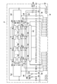
- FIG. 1 is a plan view of a multiple substrate according to an embodiment of the present invention.
- FIG. 2 is an enlarged view of a cross section taken along line II-II of the multi-faceted substrate shown in FIG. It is a figure which shows the circuit of a product area
- FIG. 1 is a plan view of a multi-faceted substrate according to an embodiment of the present invention.
- the multi-chamfered substrate 10 has a plurality of product areas P.
- the product area P is an area to be cut out to the display panel.
- the display panel is an organic electroluminescence panel, and for example, unit pixels (sub-pixels) of plural colors of red, green and blue are combined to form a full-color pixel (pixel), and a full-color image is displayed in the display area DA. It is supposed to be displayed on.
- the multi-chamfered substrate 10 has a blank area M adjacent to each of the plurality of product areas P.
- FIG. 2 is an enlarged view of a cross section taken along line II-II of the substrate 10 shown in FIG.
- the multi-chamfered substrate 10 has a substrate 12.
- An undercoat layer 14 serving as a barrier to impurities is formed on the substrate 12, and a semiconductor layer 16 is formed thereon.
- the source electrode 18 and the drain electrode 20 are electrically connected to the semiconductor layer 16, and the gate insulating film 22 is formed to cover the semiconductor layer 16.
- a gate electrode 24 is formed on the gate insulating film 22, and an interlayer insulating film 26 is formed to cover the gate electrode 24.
- the source electrode 18 and the drain electrode 20 penetrate the gate insulating film 22 and the interlayer insulating film 26.
- the semiconductor layer 16, the source electrode 18, the drain electrode 20 and the gate electrode 24 constitute at least a part of the thin film transistor TFT.
- a passivation film 28 is provided to cover the thin film transistor TFT.
- a planarization layer 30 is provided on the passivation film 28.
- a plurality of pixel electrodes 32 eg, anodes
- the planarization layer 30 is formed such that at least the surface on which the pixel electrode 32 is provided is flat.
- the pixel electrode 32 is electrically connected to one of the source electrode 18 and the drain electrode 20 on the semiconductor layer 16 by a contact hole 34 penetrating the planarization layer 30 and the passivation film 28.
- An insulating layer 36 is formed on the planarization layer 30 and the pixel electrode 32.
- the insulating layer 36 is formed on the peripheral portion of the pixel electrode 32 so as to open a part (for example, the central portion) of the pixel electrode 32.
- the insulating layer 36 forms a bank surrounding a part of the pixel electrode 32.
- the pixel electrode 32 is a part of the light emitting element 38.
- the light emitting element 38 includes an opposing electrode 40 (for example, a cathode) facing the plurality of pixel electrodes 32 and an organic electroluminescent layer 42.
- the organic electroluminescent layer 42 includes a light emitting layer EML.
- the light emitting layer EML is provided separately (separately) for each of the pixel electrodes 32 and is also placed on the insulating layer 36.
- the light emitting layer EML emits light in blue, red or green corresponding to each pixel.
- the color corresponding to each pixel is not limited to this, and may be yellow or white, for example.
- the light emitting layer EML is formed, for example, by vapor deposition.
- the light emitting layer EML may be formed on the entire surface covering the display area DA shown in FIG. 1 so as to extend over a plurality of pixels. That is, the light emitting layer EML may be formed on the insulating layer 36 so as to be continuous.
- the light emitting layer EML is formed by application by solvent dispersion.
- the light emitting layer EML is formed to extend over a plurality of pixels, light emission is performed in white in all sub-pixels, and a desired color wavelength portion is extracted through a color filter (not shown).
- a hole injecting and transporting layer HITL made of at least one of a hole injecting layer and a hole transporting layer is interposed.
- the hole injection transport layer HITL may be provided separately for each pixel electrode 32, but in the example of FIG. 2, it is continuous throughout the display area DA (see FIG. 1).
- the hole injection transport layer HITL is in contact with the pixel electrode 32 and the insulating layer 36.
- an electron injecting and transporting layer EITL formed of at least one of the electron injecting layer and the electron transporting layer is interposed.
- the electron injecting and transporting layer EITL may be provided separately for each pixel electrode 32, but in the example of FIG. 2, it is continuous over the entire display area DA.
- the electron injection transport layer EITL is in contact with the counter electrode 40.
- the light emitting layer EML is sandwiched between the pixel electrode 32 and the counter electrode 40, and the luminance is controlled by the current flowing between the two to emit light.
- a light emitting element 38 is provided so as to be driven by current.
- the counter electrode 40 is made of a metal thin film or the like and has light transparency, and transmits light generated in the light emitting layer EML to display an image.
- the pixel electrode 32 may be a reflective film that reflects light generated in the light emitting layer EML in the direction of the counter electrode 40, and one of the plurality of layers may be a reflective film.
- the organic electroluminescent layer 42 is sealed by the sealing film 44 and blocked from moisture.
- the sealing film 44 may include an inorganic layer made of an inorganic layer material such as silicon nitride, and the pair of inorganic layers may sandwich the organic layer.
- the opposing substrate 48 is attached to the sealing film 44 via the adhesive layer 46.
- FIG. 3 is a diagram showing a circuit of the product area P.
- a plurality of light emitting elements 38 for generating an image are driven for each scanning line 50 by a line sequential scanning method.
- a plurality of scan lines 50 are drawn from the scan circuit 52.
- a power supply line 54 (a cathode line and an anode line) for supplying a current is connected to the light emitting element 38.
- a signal line 56 is connected to the light emitting element 38 in order to input an image signal for controlling a current.
- a signal line selection circuit 58 for selecting one of the plurality of signal lines 56 is provided, and a cell inspection circuit 60 for inspecting all the light emitting elements 38 at one time is provided.
- a plurality of product pads 62 are arranged.
- the product pad 62 is used in the cut out display panel.
- the plurality of product pads 62 include pads for supplying power to the scanning circuit 52, pads for inputting control signals to the scanning circuit 52, pads for inputting control signals to the signal line selection circuit 58, and the like.
- the plurality of product pads 62 include power supply pads 64 (product cathode pads and product anode pads) connected to power supply lines 54 for supplying current to the light emitting elements 38.
- a plurality of first inspection pads 66 are disposed to inspect the light emitting elements 38.
- the plurality of first test pads 66 include a cathode pad 68 and an anode pad 70 for supplying a current to the light emitting device 38.
- the cathode pad 68 and the anode pad 70 are connected to the power supply pad 64 (product cathode pad and product anode pad), respectively.
- the plurality of first test pads 66 are closer to the plurality of light emitting elements 38 than the plurality of product pads 62.
- a plurality of second inspection pads 72 are arranged corresponding to the respective product areas P in order to inspect the light emitting elements 38.
- the plurality of second test pads 72 are a pad for supplying power to the scanning circuit 52, a pad for inputting a control signal to the scanning circuit 52, a pad for inputting a control signal to the signal line selection circuit 58, and a cell It includes a pad and the like for inputting a control signal to inspection circuit 60.
- the plurality of second test pads 72 do not include pads for flowing current for causing the light emitting element 38 to emit light.
- the inspection pad can be efficiently arranged in the restricted space. become.
- FIG. 1 A current is supplied through the cathode pad 68 and the anode pad 70 to inspect the light emitting element 38. Then, a plurality of display panels are cut out from the multiple substrate 10 so as to correspond to the plurality of product areas P, respectively.
- the wires 74 connected to the plurality of second test pads 72 have narrow portions 74 a narrowed on the cutting lines so as to be easily cut (see FIG. 1).
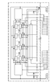
- FIG. 4 is a diagram showing a circuit of a product area P according to a modification of the embodiment of the present invention.
- the cathode pad 168 and the anode pad 170 are used not only for testing the light emitting element 138 but also for products. That is, the cathode pad 168 and the anode pad 170 are also used to supply current to the light emitting element 138 in each of the plurality of display panels cut out.
- a plurality of product pads 162 for use in each of the plurality of display panels cut out for applications other than flowing current to the light emitting element 138 are disposed.
- the cathode pad 168 and the anode pad 170 have a large area, or the distance between adjacent pads is wide. This makes it easier to apply a test probe to the cathode pad 168 and the anode pad 170.
- the method for manufacturing a display device according to the present embodiment corresponds to the obvious contents from the above description of the structure and the contents described in the above embodiment.
- the display device is not limited to the organic electroluminescence display device, and may be a display device provided with a light emitting element such as a quantum dot light emitting element (QLED: Quantum-Dot Light Emitting Diode) in each pixel.
- a light emitting element such as a quantum dot light emitting element (QLED: Quantum-Dot Light Emitting Diode) in each pixel.
- QLED Quantum-Dot Light Emitting Diode
- the present invention is not limited to the above-described embodiment, and various modifications are possible.
- the configurations described in the embodiments can be replaced with configurations that have substantially the same configuration, configurations having the same effects, or configurations that can achieve the same purpose.
Landscapes
- Engineering & Computer Science (AREA)
- Manufacturing & Machinery (AREA)
- Microelectronics & Electronic Packaging (AREA)
- Physics & Mathematics (AREA)
- General Physics & Mathematics (AREA)
- Theoretical Computer Science (AREA)
- Computer Hardware Design (AREA)
- Electroluminescent Light Sources (AREA)
- Devices For Indicating Variable Information By Combining Individual Elements (AREA)
Abstract
電流で駆動される発光素子(38)がそれぞれに設けられた複数の製品領域(P)と、複数の製品領域(P)のそれぞれに隣接する余白領域(M)と、を一体的に有する多面取り基板(10)を用意する。陰極パッド(68)及び陽極パッド(70)を通して電流を流して発光素子(38)を検査する。多面取り基板(10)から、複数の製品領域(P)にそれぞれ対応するように、複数の表示パネルを切り出す。多面取り基板(10)は、発光素子(38)を検査するために複数の製品領域(P)のそれぞれに配置された複数の第1検査パッド(66)と、発光素子(38)を検査するために余白領域(M)に配置された複数の第2検査パッド(72)と、を有する。陰極パッド(68)及び陽極パッド(70)は、複数の第1検査パッド(66)に含まれ、複数の第2検査パッド(72)に含まれない。
Description
本発明は、表示装置の製造方法及び多面取り基板に関する。
多面取り基板を使用して複数の表示パネルを一体的に製造し、その後、個々の表示パネルを切り出すことが知られている(特許文献1)。このような多面取り方式の製造プロセスでは、個々の表示パネルに切断する前にセル検査を行う。セル検査のための検査パッドは、表示パネルごとに、表示領域の外側にある周辺領域に配置されていた。
近年、表示領域を広くするために周辺領域が狭くなる傾向にあり、周辺領域には検査パッドを配置するスペースがなくなってきた。そこで、多面取り基板において、製品領域の外側に検査パッドを配置することが多くなってきた。
有機エレクトロルミネッセンス表示装置のように、発光素子を電流駆動する場合、電流を供給するための検査パッドが製品領域の外側にあると配線が長くなる。あるいは、切断を容易に行えるように、切断ラインと交差する部分で配線を細くすることがある。そのため、電圧降下によって正確な検査ができなかったり、発熱によって発光素子に影響を与えたりする。
本発明は、制約されたスペースで検査パッドを効率的に配置することを目的とする。
本発明に係る表示装置の製造方法は、電流で駆動される発光素子がそれぞれに設けられた複数の製品領域と、前記複数の製品領域のそれぞれに隣接する余白領域と、を一体的に有する多面取り基板を用意する工程と、陰極パッド及び陽極パッドを通して前記電流を流して前記発光素子を検査する工程と、前記多面取り基板から、前記複数の製品領域にそれぞれ対応するように、複数の表示パネルを切り出す工程と、を含み、前記多面取り基板は、前記発光素子を検査するために前記複数の製品領域のそれぞれに配置された複数の第1検査パッドと、前記発光素子を検査するために前記余白領域に配置された複数の第2検査パッドと、を有し、前記陰極パッド及び前記陽極パッドは、前記複数の第1検査パッドに含まれ、前記複数の第2検査パッドに含まれないことを特徴とする。
本発明によれば、電流を流すための陰極パッド及び陽極パッドを製品領域内に配置することで、制約されたスペースで検査パッドを効率的に配置することが可能になる。
本発明に係る多面取り基板は、複数の表示パネルに切り出されるための複数の製品領域のそれぞれに、電流で駆動されるように設けられた発光素子と、前記発光素子を検査するために、前記複数の製品領域のそれぞれに配置された複数の第1検査パッドと、前記発光素子を検査するために、前記複数の製品領域のそれぞれに隣接する余白領域に配置された複数の第2検査パッドと、前記複数の第1検査パッドは、前記電流を流すための陰極パッド及び陽極パッドを含み、前記複数の第2検査パッドは、前記電流を流すためのパッドを含まないことを特徴とする。
本発明によれば、電流を流すための陰極パッド及び陽極パッドを製品領域内に配置することで、制約されたスペースで検査パッドを効率的に配置することが可能になる。
以下、本発明の実施形態について図面を参照して説明する。但し、本発明は、その要旨を逸脱しない範囲において様々な態様で実施することができ、以下に例示する実施形態の記載内容に限定して解釈されるものではない。
図面は、説明をより明確にするため、実際の態様に比べ、各部の幅、厚さ、形状等について模式的に表される場合があるが、あくまで一例であって、本発明の解釈を限定するものではない。本明細書と各図において、既出の図に関して説明したものと同様の機能を備えた要素には、同一の符号を付して、重複する説明を省略することがある。
さらに、本発明の詳細な説明において、ある構成物と他の構成物の位置関係を規定する際、「上に」「下に」とは、ある構成物の直上あるいは直下に位置する場合のみでなく、特に断りの無い限りは、間にさらに他の構成物を介在する場合を含むものとする。
図1は、本発明の実施形態に係る多面取り基板の平面図である。多面取り基板10は、複数の製品領域Pを有する。製品領域Pは表示パネルに切り出されるための領域である。表示パネルは、有機エレクトロルミネッセンスパネルであり、例えば、赤、緑及び青からなる複数色の単位画素(サブピクセル)を組み合わせて、フルカラーの画素(ピクセル)を形成し、フルカラーの画像を表示領域DAに表示するようになっている。多面取り基板10は、複数の製品領域Pのそれぞれに隣接する余白領域Mを有する。
図2は、図1に示す多面取り基板10のII-II線断面の拡大図である。多面取り基板10は、基板12を有する。基板12には、不純物に対するバリアとなるアンダーコート層14が形成され、その上に半導体層16が形成されている。半導体層16にソース電極18及びドレイン電極20が電気的に接続し、半導体層16を覆ってゲート絶縁膜22が形成されている。ゲート絶縁膜22の上にはゲート電極24が形成され、ゲート電極24を覆って層間絶縁膜26が形成されている。ソース電極18及びドレイン電極20は、ゲート絶縁膜22及び層間絶縁膜26を貫通している。半導体層16、ソース電極18、ドレイン電極20及びゲート電極24によって薄膜トランジスタTFTの少なくとも一部が構成される。薄膜トランジスタTFTを覆うようにパッシベーション膜28が設けられている。
パッシベーション膜28の上には、平坦化層30が設けられている。平坦化層30の上には、複数の単位画素それぞれに対応するように構成された複数の画素電極32(例えば陽極)が設けられている。平坦化層30は、少なくとも画素電極32が設けられる面が平坦になるように形成される。画素電極32は、平坦化層30及びパッシベーション膜28を貫通するコンタクトホール34によって、半導体層16上のソース電極18及びドレイン電極20の一方に電気的に接続している。
平坦化層30及び画素電極32上に、絶縁層36が形成されている。絶縁層36は、画素電極32の周縁部に載り、画素電極32の一部(例えば中央部)を開口させるように形成されている。絶縁層36によって、画素電極32の一部を囲むバンクが形成される。画素電極32は、発光素子38の一部である。発光素子38は、複数の画素電極32に対向する対向電極40(例えば陰極)と有機エレクトロルミネッセンス層42を含む。
有機エレクトロルミネッセンス層42は、発光層EMLを含む。発光層EMLは、画素電極32ごとに別々に(分離して)設けられ、絶縁層36にも載るようになっている。この場合は各画素に対応して青、赤又は緑で発光層EMLが発光するようになる。各画素に対応する色はこれに限られず、例えば、黄又は白等でもよい。発光層EMLは、例えば、蒸着により形成される。あるいは、発光層EMLは、図1に示す表示領域DAを覆う全面に、複数の画素に亘るように形成してもよい。つまり、発光層EMLを絶縁層36上で連続するように形成してもよい。この場合、発光層EMLは溶媒分散による塗布により形成する。発光層EMLを複数の画素に亘るように形成する場合は、全サブピクセルにおいて白色で発光し、図示しないカラーフィルタを通して所望の色波長部分を取り出す構成になる。
画素電極32と発光層EMLとの間に、正孔注入層及び正孔輸送層の少なくとも一方からなる正孔注入輸送層HITLが介在する。正孔注入輸送層HITLは、1つの画素電極32ごとに分離して設けてもよいが、図2の例では表示領域DA(図1参照)の全体にわたって連続している。正孔注入輸送層HITLは、画素電極32及び絶縁層36に接触するようになっている。
対向電極40と発光層EMLとの間に、電子注入層及び電子輸送層の少なくとも一方からなる電子注入輸送層EITLが介在する。電子注入輸送層EITLは、1つの画素電極32ごとに分離して設けてもよいが、図2の例では表示領域DAの全体にわたって連続している。電子注入輸送層EITLは、対向電極40に接触するようになっている。
発光層EMLは、画素電極32及び対向電極40に挟まれ、両者間を流れる電流によって輝度が制御されて発光する。製品領域Pには、電流で駆動されるように発光素子38が設けられている。対向電極40は、金属薄膜などからなり光透過性を有し、発光層EMLで生じた光を透過させて画像を表示する。画素電極32は、発光層EMLで生じた光を対向電極40の方向に反射する反射膜からなり、複数層の1層が反射膜であってもよい。
有機エレクトロルミネッセンス層42は、封止膜44によって封止されて水分から遮断される。封止膜44は、窒化ケイ素などの無機層材料からなる無機層を含み、一対の無機層が有機層を挟む構造であってもよい。封止膜44には、粘着層46を介して、対向基板48が貼り付けられている。
図3は、製品領域Pの回路を示す図である。画像を生成するための複数の発光素子38は、線順次走査方式によって走査線50ごとに駆動される。複数の走査線50は走査回路52から引き出されている。発光素子38には、電流を供給するための電源線54(陰極線及び陽極線)が接続される。また、発光素子38には、電流を制御するための画像信号を入力するために信号線56が接続される。なお、複数の信号線56のいずれかを選択するための信号線選択回路58が設けられ、全ての発光素子38を一括して検査するためのセル検査回路60が設けられている。
製品領域Pには、複数の製品パッド62が配置されている。製品パッド62は、切り出された表示パネルで使用される。複数の製品パッド62は、走査回路52に電源を供給するためのパッド、走査回路52に制御信号を入力するためのパッド、信号線選択回路58に制御信号を入力するためのパッドなどを含む。さらに、複数の製品パッド62は、発光素子38に電流を供給するための電源線54に接続される電源パッド64(製品陰極パッド及び製品陽極パッド)を含む。
製品領域Pには、発光素子38を検査するために、複数の第1検査パッド66が配置されている。複数の第1検査パッド66は、発光素子38に電流を流すための陰極パッド68及び陽極パッド70を含む。陰極パッド68及び陽極パッド70は、それぞれ、電源パッド64(製品陰極パッド及び製品陽極パッド)に接続されている。複数の第1検査パッド66は、複数の製品パッド62よりも、複数の発光素子38に近い位置にある。
余白領域Mには、発光素子38を検査するために、それぞれの製品領域Pに対応して複数の第2検査パッド72が配置されている。複数の第2検査パッド72は、走査回路52に電源を供給するためのパッド、走査回路52に制御信号を入力するためのパッド、信号線選択回路58に制御信号を入力するためのパッド、セル検査回路60に制御信号を入力するためのパッドなどを含む。複数の第2検査パッド72は、発光素子38を発光させるための電流を流すためのパッドは含まない。
本実施形態によれば、発光素子38に電流を流すための陰極パッド68及び陽極パッド70を製品領域P内に配置することで、制約されたスペースで検査パッドを効率的に配置することが可能になる。
本実施形態に係る表示装置の製造方法では、図1に示すように、多面取り基板10を用意する。陰極パッド68及び陽極パッド70を通して電流を流して発光素子38を検査する。そして、多面取り基板10から、複数の製品領域Pにそれぞれ対応するように、複数の表示パネルを切り出す。なお、複数の第2検査パッド72に接続される配線74は、切断しやすいように、切断ライン上に細くなった幅狭部74aを有する(図1参照)。
図4は、本発明の実施形態の変形例に係る製品領域Pの回路を示す図である。この例では、陰極パッド168及び陽極パッド170は、発光素子138を検査するためだけでなく、製品にも使用される。つまり、陰極パッド168及び陽極パッド170は、切り出された複数の表示パネルのそれぞれで、電流を発光素子138に流すためにも兼用される。
製品領域Pには、電流を発光素子138に流す以外の用途で、切り出された複数の表示パネルのそれぞれで使用するための複数の製品パッド162が配置されている。製品パッド162と比べて、陰極パッド168及び陽極パッド170は、面積が大きいか、あるいは、隣のパッドとの間隔が広くなっている。こうすることで、陰極パッド168及び陽極パッド170に、検査用のプローブを当て易くなる。本実施形態に係る表示装置の製造方法は、上記構造に関する説明から自明の内容及び上記実施形態で説明した内容が該当する。
なお、表示装置は、有機エレクトロルミネッセンス表示装置には限定されず、量子ドット発光素子(QLED:Quantum‐Dot Light Emitting Diode)のような発光素子を各画素に備えた表示装置であってもよい。
本発明は、上述した実施形態に限定されるものではなく種々の変形が可能である。例えば、実施形態で説明した構成は、実質的に同一の構成、同一の作用効果を奏する構成又は同一の目的を達成することができる構成で置き換えることができる。
Claims (8)
- 電流で駆動される発光素子がそれぞれに設けられた複数の製品領域と、前記複数の製品領域のそれぞれに隣接する余白領域と、を一体的に有する多面取り基板を用意する工程と、
陰極パッド及び陽極パッドを通して前記電流を流して前記発光素子を検査する工程と、
前記多面取り基板から、前記複数の製品領域にそれぞれ対応するように、複数の表示パネルを切り出す工程と、
を含み、
前記多面取り基板は、前記発光素子を検査するために前記複数の製品領域のそれぞれに配置された複数の第1検査パッドと、前記発光素子を検査するために前記余白領域に配置された複数の第2検査パッドと、を有し、
前記陰極パッド及び前記陽極パッドは、前記複数の第1検査パッドに含まれ、前記複数の第2検査パッドに含まれないことを特徴とする表示装置の製造方法。 - 請求項1に記載された表示装置の製造方法において、
前記多面取り基板は、前記複数の製品領域のそれぞれに、切り出された前記複数の表示パネルのそれぞれで使用するための複数の製品パッドをさらに有することを特徴とする表示装置の製造方法。 - 請求項1に記載された表示装置の製造方法において、
前記陰極パッド及び前記陽極パッドは、切り出された前記複数の表示パネルのそれぞれで前記電流を前記発光素子に流すためにも兼用されることを特徴とする表示装置の製造方法。 - 請求項3に記載された表示装置の製造方法において、
前記多面取り基板は、前記複数の製品領域のそれぞれに、前記電流を前記発光素子に流す以外の用途で、切り出された前記複数の表示パネルのそれぞれで使用するための複数の製品パッドをさらに有することを特徴とする表示装置の製造方法。 - 複数の表示パネルに切り出されるための複数の製品領域のそれぞれに、電流で駆動されるように設けられた発光素子と、
前記発光素子を検査するために、前記複数の製品領域のそれぞれに配置された複数の第1検査パッドと、
前記発光素子を検査するために、前記複数の製品領域のそれぞれに隣接する余白領域に配置された複数の第2検査パッドと、
前記複数の第1検査パッドは、前記電流を流すための陰極パッド及び陽極パッドを含み、
前記複数の第2検査パッドは、前記電流を流すためのパッドを含まないことを特徴とする多面取り基板。 - 請求項5に記載された多面取り基板において、
前記複数の製品領域のそれぞれに、切り出された前記複数の表示パネルのそれぞれで使用するための複数の製品パッドをさらに有することを特徴とする多面取り基板。 - 請求項5に記載された多面取り基板において、
前記陰極パッド及び前記陽極パッドは、切り出された前記複数の表示パネルのそれぞれで前記電流を前記発光素子に流すためにも兼用されることを特徴とする多面取り基板。 - 請求項7に記載された多面取り基板において、
前記複数の製品領域のそれぞれに、前記電流を前記発光素子に流す以外の用途で、切り出された前記複数の表示パネルのそれぞれで使用するための複数の製品パッドをさらに有することを特徴とする多面取り基板。
Priority Applications (2)
| Application Number | Priority Date | Filing Date | Title |
|---|---|---|---|
| CN201880051690.XA CN111033600B (zh) | 2017-09-07 | 2018-06-08 | 显示装置的制造方法及拼版基板 |
| US16/781,009 US11322571B2 (en) | 2017-09-07 | 2020-02-04 | Display apparatus including negative electrode pads and positive electrode pads that are included in first inspection pads but not in second inspection pads |
Applications Claiming Priority (2)
| Application Number | Priority Date | Filing Date | Title |
|---|---|---|---|
| JP2017171933A JP7001398B2 (ja) | 2017-09-07 | 2017-09-07 | 表示装置の製造方法及び多面取り基板 |
| JP2017-171933 | 2017-09-07 |
Related Child Applications (1)
| Application Number | Title | Priority Date | Filing Date |
|---|---|---|---|
| US16/781,009 Continuation US11322571B2 (en) | 2017-09-07 | 2020-02-04 | Display apparatus including negative electrode pads and positive electrode pads that are included in first inspection pads but not in second inspection pads |
Publications (1)
| Publication Number | Publication Date |
|---|---|
| WO2019049448A1 true WO2019049448A1 (ja) | 2019-03-14 |
Family
ID=65634759
Family Applications (1)
| Application Number | Title | Priority Date | Filing Date |
|---|---|---|---|
| PCT/JP2018/021988 Ceased WO2019049448A1 (ja) | 2017-09-07 | 2018-06-08 | 表示装置の製造方法及び多面取り基板 |
Country Status (4)
| Country | Link |
|---|---|
| US (1) | US11322571B2 (ja) |
| JP (1) | JP7001398B2 (ja) |
| CN (1) | CN111033600B (ja) |
| WO (1) | WO2019049448A1 (ja) |
Families Citing this family (5)
| Publication number | Priority date | Publication date | Assignee | Title |
|---|---|---|---|---|
| CN111933066A (zh) * | 2020-08-28 | 2020-11-13 | 京东方科技集团股份有限公司 | Oled显示基板、显示模组、显示面板 |
| JP7684851B2 (ja) * | 2021-06-29 | 2025-05-28 | 株式会社ジャパンディスプレイ | 表示装置 |
| CN115692424B (zh) * | 2021-07-30 | 2025-06-20 | 北京京东方光电科技有限公司 | 显示面板以及显示面板母板 |
| CN113809134B (zh) * | 2021-08-26 | 2024-06-28 | 湖北长江新型显示产业创新中心有限公司 | 一种显示面板及显示装置 |
| CN114023914A (zh) * | 2021-12-07 | 2022-02-08 | 南京迪钛飞光电科技有限公司 | 一种有机发光器件测试装置 |
Citations (5)
| Publication number | Priority date | Publication date | Assignee | Title |
|---|---|---|---|---|
| JP2008304880A (ja) * | 2007-06-05 | 2008-12-18 | Samsung Sdi Co Ltd | 有機電界発光表示装置及び有機電界発光表示装置のマザー基板 |
| US20100112887A1 (en) * | 2008-10-31 | 2010-05-06 | Kwang-Min Kim | Method of making organic light emitting display device |
| JP2011134489A (ja) * | 2009-12-22 | 2011-07-07 | Hitachi High-Technologies Corp | 有機elディスプレイ基板の点灯検査設備及び点灯検査方法、有機elディスプレイ基板の欠陥検査修正装置及び欠陥検査修正方法並びに有機elディスプレイ製造システム及び製造方法。 |
| JP2015056335A (ja) * | 2013-09-13 | 2015-03-23 | セイコーエプソン株式会社 | 電気光学装置、電子機器及び電気光学装置の製造方法 |
| JP2016065990A (ja) * | 2014-09-25 | 2016-04-28 | 株式会社ジャパンディスプレイ | 表示装置の製造方法および表示装置 |
Family Cites Families (7)
| Publication number | Priority date | Publication date | Assignee | Title |
|---|---|---|---|---|
| US7503821B2 (en) * | 2004-07-23 | 2009-03-17 | Lg Display Co., Ltd. | Mother glass and method of fabricating organic electro luminescence display device using the same |
| KR100637065B1 (ko) * | 2004-12-29 | 2006-10-23 | 엘지전자 주식회사 | 유기전계발광표시소자용 모기판 및 이를 이용한유기전계발광표시소자의 제조방법 |
| KR100840091B1 (ko) * | 2007-08-17 | 2008-06-20 | 삼성에스디아이 주식회사 | 유기전계발광 표시장치 및 그의 모기판 |
| JP2010139962A (ja) * | 2008-12-15 | 2010-06-24 | Toshiba Mobile Display Co Ltd | アレイ基板、平面表示装置、マザー基板及びアレイ基板の製造方法 |
| KR102231898B1 (ko) | 2013-12-13 | 2021-03-25 | 엘지디스플레이 주식회사 | 표시장치 및 표시패널 |
| JP2015169760A (ja) * | 2014-03-06 | 2015-09-28 | 株式会社ジャパンディスプレイ | 表示装置の製造方法、表示装置および表示装置形成基板 |
| JP6329795B2 (ja) | 2014-03-27 | 2018-05-23 | 株式会社ジャパンディスプレイ | El表示装置及びel表示装置の製造方法 |
-
2017
- 2017-09-07 JP JP2017171933A patent/JP7001398B2/ja active Active
-
2018
- 2018-06-08 WO PCT/JP2018/021988 patent/WO2019049448A1/ja not_active Ceased
- 2018-06-08 CN CN201880051690.XA patent/CN111033600B/zh active Active
-
2020
- 2020-02-04 US US16/781,009 patent/US11322571B2/en active Active
Patent Citations (5)
| Publication number | Priority date | Publication date | Assignee | Title |
|---|---|---|---|---|
| JP2008304880A (ja) * | 2007-06-05 | 2008-12-18 | Samsung Sdi Co Ltd | 有機電界発光表示装置及び有機電界発光表示装置のマザー基板 |
| US20100112887A1 (en) * | 2008-10-31 | 2010-05-06 | Kwang-Min Kim | Method of making organic light emitting display device |
| JP2011134489A (ja) * | 2009-12-22 | 2011-07-07 | Hitachi High-Technologies Corp | 有機elディスプレイ基板の点灯検査設備及び点灯検査方法、有機elディスプレイ基板の欠陥検査修正装置及び欠陥検査修正方法並びに有機elディスプレイ製造システム及び製造方法。 |
| JP2015056335A (ja) * | 2013-09-13 | 2015-03-23 | セイコーエプソン株式会社 | 電気光学装置、電子機器及び電気光学装置の製造方法 |
| JP2016065990A (ja) * | 2014-09-25 | 2016-04-28 | 株式会社ジャパンディスプレイ | 表示装置の製造方法および表示装置 |
Also Published As
| Publication number | Publication date |
|---|---|
| US11322571B2 (en) | 2022-05-03 |
| CN111033600A (zh) | 2020-04-17 |
| JP7001398B2 (ja) | 2022-01-19 |
| US20200176546A1 (en) | 2020-06-04 |
| CN111033600B (zh) | 2021-11-30 |
| JP2019045823A (ja) | 2019-03-22 |
Similar Documents
| Publication | Publication Date | Title |
|---|---|---|
| US11322571B2 (en) | Display apparatus including negative electrode pads and positive electrode pads that are included in first inspection pads but not in second inspection pads | |
| US9305981B2 (en) | Organic electro-luminescent device | |
| US10062870B2 (en) | Display device including a diffraction grating | |
| CN103794175B (zh) | 显示装置及修复该显示装置的方法 | |
| US9035286B2 (en) | Multi-color light emitting diode and method for making same | |
| JP6842362B2 (ja) | 表示装置 | |
| JP2015135438A (ja) | 発光素子表示装置 | |
| CN108682324B (zh) | 无机发光二极管显示面板和显示装置 | |
| US9882174B2 (en) | Repairing method, repairing device and manufacturing method of array substrate | |
| US20220093888A1 (en) | Organic device | |
| JP2003257667A (ja) | 有機電界発光素子及びその製造方法 | |
| US11018200B2 (en) | Display device having a white emitting area | |
| US9362342B2 (en) | Light-emitting element display device | |
| KR20170113866A (ko) | 디스플레이장치 | |
| US20220165976A1 (en) | Display device | |
| KR20160038494A (ko) | 유기발광표시장치 및 그 제조 방법 | |
| US20150090987A1 (en) | Organic el display device | |
| KR20190079308A (ko) | 전계발광 표시장치 | |
| KR20150030069A (ko) | 유기 발광 표시 장치 및 그 제조 방법 | |
| KR20150113530A (ko) | 유기 발광 표시 장치 | |
| JP2018006232A (ja) | 表示装置及びその製造方法 | |
| US20210098548A1 (en) | Display device | |
| EP3113227B1 (en) | Organic light emitting display device | |
| US11138931B2 (en) | Display device and manufacturing method therefor | |
| JP2016096076A (ja) | 有機el表示装置及びその製造方法 |
Legal Events
| Date | Code | Title | Description |
|---|---|---|---|
| 121 | Ep: the epo has been informed by wipo that ep was designated in this application |
Ref document number: 18854962 Country of ref document: EP Kind code of ref document: A1 |
|
| NENP | Non-entry into the national phase |
Ref country code: DE |
|
| 122 | Ep: pct application non-entry in european phase |
Ref document number: 18854962 Country of ref document: EP Kind code of ref document: A1 |