WO2019044948A1 - 電力変換装置 - Google Patents
電力変換装置 Download PDFInfo
- Publication number
- WO2019044948A1 WO2019044948A1 PCT/JP2018/032058 JP2018032058W WO2019044948A1 WO 2019044948 A1 WO2019044948 A1 WO 2019044948A1 JP 2018032058 W JP2018032058 W JP 2018032058W WO 2019044948 A1 WO2019044948 A1 WO 2019044948A1
- Authority
- WO
- WIPO (PCT)
- Prior art keywords
- refrigerant flow
- capacitor
- flow passage
- reactor
- refrigerant
- Prior art date
- Legal status (The legal status is an assumption and is not a legal conclusion. Google has not performed a legal analysis and makes no representation as to the accuracy of the status listed.)
- Ceased
Links
Images

Classifications
-
- B—PERFORMING OPERATIONS; TRANSPORTING
- B60—VEHICLES IN GENERAL
- B60L—PROPULSION OF ELECTRICALLY-PROPELLED VEHICLES; SUPPLYING ELECTRIC POWER FOR AUXILIARY EQUIPMENT OF ELECTRICALLY-PROPELLED VEHICLES; ELECTRODYNAMIC BRAKE SYSTEMS FOR VEHICLES IN GENERAL; MAGNETIC SUSPENSION OR LEVITATION FOR VEHICLES; MONITORING OPERATING VARIABLES OF ELECTRICALLY-PROPELLED VEHICLES; ELECTRIC SAFETY DEVICES FOR ELECTRICALLY-PROPELLED VEHICLES
- B60L15/00—Methods, circuits, or devices for controlling the traction-motor speed of electrically-propelled vehicles
- B60L15/007—Physical arrangements or structures of drive train converters specially adapted for the propulsion motors of electric vehicles
-
- H—ELECTRICITY
- H02—GENERATION; CONVERSION OR DISTRIBUTION OF ELECTRIC POWER
- H02M—APPARATUS FOR CONVERSION BETWEEN AC AND AC, BETWEEN AC AND DC, OR BETWEEN DC AND DC, AND FOR USE WITH MAINS OR SIMILAR POWER SUPPLY SYSTEMS; CONVERSION OF DC OR AC INPUT POWER INTO SURGE OUTPUT POWER; CONTROL OR REGULATION THEREOF
- H02M7/00—Conversion of AC power input into DC power output; Conversion of DC power input into AC power output
- H02M7/42—Conversion of DC power input into AC power output without possibility of reversal
- H02M7/44—Conversion of DC power input into AC power output without possibility of reversal by static converters
- H02M7/48—Conversion of DC power input into AC power output without possibility of reversal by static converters using discharge tubes with control electrode or semiconductor devices with control electrode
- H02M7/53—Conversion of DC power input into AC power output without possibility of reversal by static converters using discharge tubes with control electrode or semiconductor devices with control electrode using devices of a triode or transistor type requiring continuous application of a control signal
- H02M7/537—Conversion of DC power input into AC power output without possibility of reversal by static converters using discharge tubes with control electrode or semiconductor devices with control electrode using devices of a triode or transistor type requiring continuous application of a control signal using semiconductor devices only, e.g. single switched pulse inverters
-
- H—ELECTRICITY
- H05—ELECTRIC TECHNIQUES NOT OTHERWISE PROVIDED FOR
- H05K—PRINTED CIRCUITS; CASINGS OR CONSTRUCTIONAL DETAILS OF ELECTRIC APPARATUS; MANUFACTURE OF ASSEMBLAGES OF ELECTRICAL COMPONENTS
- H05K7/00—Constructional details common to different types of electric apparatus
- H05K7/20—Modifications to facilitate cooling, ventilating, or heating
- H05K7/2089—Modifications to facilitate cooling, ventilating, or heating for power electronics, e.g. for inverters for controlling motor
- H05K7/20927—Liquid coolant without phase change
-
- H—ELECTRICITY
- H10—SEMICONDUCTOR DEVICES; ELECTRIC SOLID-STATE DEVICES NOT OTHERWISE PROVIDED FOR
- H10W—GENERIC PACKAGES, INTERCONNECTIONS, CONNECTORS OR OTHER CONSTRUCTIONAL DETAILS OF DEVICES COVERED BY CLASS H10
- H10W40/00—Arrangements for thermal protection or thermal control
- H10W40/20—Arrangements for cooling
- H10W40/22—Arrangements for cooling characterised by their shape, e.g. having conical or cylindrical projections
-
- H—ELECTRICITY
- H10—SEMICONDUCTOR DEVICES; ELECTRIC SOLID-STATE DEVICES NOT OTHERWISE PROVIDED FOR
- H10W—GENERIC PACKAGES, INTERCONNECTIONS, CONNECTORS OR OTHER CONSTRUCTIONAL DETAILS OF DEVICES COVERED BY CLASS H10
- H10W40/00—Arrangements for thermal protection or thermal control
- H10W40/40—Arrangements for thermal protection or thermal control involving heat exchange by flowing fluids
- H10W40/47—Arrangements for thermal protection or thermal control involving heat exchange by flowing fluids by flowing liquids, e.g. forced water cooling
-
- B—PERFORMING OPERATIONS; TRANSPORTING
- B60—VEHICLES IN GENERAL
- B60L—PROPULSION OF ELECTRICALLY-PROPELLED VEHICLES; SUPPLYING ELECTRIC POWER FOR AUXILIARY EQUIPMENT OF ELECTRICALLY-PROPELLED VEHICLES; ELECTRODYNAMIC BRAKE SYSTEMS FOR VEHICLES IN GENERAL; MAGNETIC SUSPENSION OR LEVITATION FOR VEHICLES; MONITORING OPERATING VARIABLES OF ELECTRICALLY-PROPELLED VEHICLES; ELECTRIC SAFETY DEVICES FOR ELECTRICALLY-PROPELLED VEHICLES
- B60L2210/00—Converter types
- B60L2210/40—DC to AC converters
-
- H—ELECTRICITY
- H02—GENERATION; CONVERSION OR DISTRIBUTION OF ELECTRIC POWER
- H02M—APPARATUS FOR CONVERSION BETWEEN AC AND AC, BETWEEN AC AND DC, OR BETWEEN DC AND DC, AND FOR USE WITH MAINS OR SIMILAR POWER SUPPLY SYSTEMS; CONVERSION OF DC OR AC INPUT POWER INTO SURGE OUTPUT POWER; CONTROL OR REGULATION THEREOF
- H02M1/00—Details of apparatus for conversion
- H02M1/0067—Converter structures employing plural converter units, other than for parallel operation of the units on a single load
- H02M1/007—Plural converter units in cascade
-
- H—ELECTRICITY
- H02—GENERATION; CONVERSION OR DISTRIBUTION OF ELECTRIC POWER
- H02M—APPARATUS FOR CONVERSION BETWEEN AC AND AC, BETWEEN AC AND DC, OR BETWEEN DC AND DC, AND FOR USE WITH MAINS OR SIMILAR POWER SUPPLY SYSTEMS; CONVERSION OF DC OR AC INPUT POWER INTO SURGE OUTPUT POWER; CONTROL OR REGULATION THEREOF
- H02M1/00—Details of apparatus for conversion
- H02M1/0067—Converter structures employing plural converter units, other than for parallel operation of the units on a single load
- H02M1/008—Plural converter units for generating at two or more independent and non-parallel outputs, e.g. systems with plural point of load switching regulators
-
- H—ELECTRICITY
- H02—GENERATION; CONVERSION OR DISTRIBUTION OF ELECTRIC POWER
- H02M—APPARATUS FOR CONVERSION BETWEEN AC AND AC, BETWEEN AC AND DC, OR BETWEEN DC AND DC, AND FOR USE WITH MAINS OR SIMILAR POWER SUPPLY SYSTEMS; CONVERSION OF DC OR AC INPUT POWER INTO SURGE OUTPUT POWER; CONTROL OR REGULATION THEREOF
- H02M3/00—Conversion of DC power input into DC power output
- H02M3/02—Conversion of DC power input into DC power output without intermediate conversion into AC
- H02M3/04—Conversion of DC power input into DC power output without intermediate conversion into AC by static converters
- H02M3/10—Conversion of DC power input into DC power output without intermediate conversion into AC by static converters using discharge tubes with control electrode or semiconductor devices with control electrode
- H02M3/145—Conversion of DC power input into DC power output without intermediate conversion into AC by static converters using discharge tubes with control electrode or semiconductor devices with control electrode using devices of a triode or transistor type requiring continuous application of a control signal
- H02M3/155—Conversion of DC power input into DC power output without intermediate conversion into AC by static converters using discharge tubes with control electrode or semiconductor devices with control electrode using devices of a triode or transistor type requiring continuous application of a control signal using semiconductor devices only
- H02M3/156—Conversion of DC power input into DC power output without intermediate conversion into AC by static converters using discharge tubes with control electrode or semiconductor devices with control electrode using devices of a triode or transistor type requiring continuous application of a control signal using semiconductor devices only with automatic control of output voltage or current, e.g. switching regulators
- H02M3/158—Conversion of DC power input into DC power output without intermediate conversion into AC by static converters using discharge tubes with control electrode or semiconductor devices with control electrode using devices of a triode or transistor type requiring continuous application of a control signal using semiconductor devices only with automatic control of output voltage or current, e.g. switching regulators including plural semiconductor devices as final control devices for a single load
-
- H—ELECTRICITY
- H02—GENERATION; CONVERSION OR DISTRIBUTION OF ELECTRIC POWER
- H02M—APPARATUS FOR CONVERSION BETWEEN AC AND AC, BETWEEN AC AND DC, OR BETWEEN DC AND DC, AND FOR USE WITH MAINS OR SIMILAR POWER SUPPLY SYSTEMS; CONVERSION OF DC OR AC INPUT POWER INTO SURGE OUTPUT POWER; CONTROL OR REGULATION THEREOF
- H02M7/00—Conversion of AC power input into DC power output; Conversion of DC power input into AC power output
- H02M7/003—Constructional details, e.g. physical layout, assembly, wiring or busbar connections
-
- H—ELECTRICITY
- H02—GENERATION; CONVERSION OR DISTRIBUTION OF ELECTRIC POWER
- H02M—APPARATUS FOR CONVERSION BETWEEN AC AND AC, BETWEEN AC AND DC, OR BETWEEN DC AND DC, AND FOR USE WITH MAINS OR SIMILAR POWER SUPPLY SYSTEMS; CONVERSION OF DC OR AC INPUT POWER INTO SURGE OUTPUT POWER; CONTROL OR REGULATION THEREOF
- H02M7/00—Conversion of AC power input into DC power output; Conversion of DC power input into AC power output
- H02M7/42—Conversion of DC power input into AC power output without possibility of reversal
- H02M7/44—Conversion of DC power input into AC power output without possibility of reversal by static converters
- H02M7/48—Conversion of DC power input into AC power output without possibility of reversal by static converters using discharge tubes with control electrode or semiconductor devices with control electrode
- H02M7/53—Conversion of DC power input into AC power output without possibility of reversal by static converters using discharge tubes with control electrode or semiconductor devices with control electrode using devices of a triode or transistor type requiring continuous application of a control signal
- H02M7/537—Conversion of DC power input into AC power output without possibility of reversal by static converters using discharge tubes with control electrode or semiconductor devices with control electrode using devices of a triode or transistor type requiring continuous application of a control signal using semiconductor devices only, e.g. single switched pulse inverters
- H02M7/5387—Conversion of DC power input into AC power output without possibility of reversal by static converters using discharge tubes with control electrode or semiconductor devices with control electrode using devices of a triode or transistor type requiring continuous application of a control signal using semiconductor devices only, e.g. single switched pulse inverters in a bridge configuration
-
- Y—GENERAL TAGGING OF NEW TECHNOLOGICAL DEVELOPMENTS; GENERAL TAGGING OF CROSS-SECTIONAL TECHNOLOGIES SPANNING OVER SEVERAL SECTIONS OF THE IPC; TECHNICAL SUBJECTS COVERED BY FORMER USPC CROSS-REFERENCE ART COLLECTIONS [XRACs] AND DIGESTS
- Y02—TECHNOLOGIES OR APPLICATIONS FOR MITIGATION OR ADAPTATION AGAINST CLIMATE CHANGE
- Y02T—CLIMATE CHANGE MITIGATION TECHNOLOGIES RELATED TO TRANSPORTATION
- Y02T10/00—Road transport of goods or passengers
- Y02T10/60—Other road transportation technologies with climate change mitigation effect
- Y02T10/64—Electric machine technologies in electromobility
-
- Y—GENERAL TAGGING OF NEW TECHNOLOGICAL DEVELOPMENTS; GENERAL TAGGING OF CROSS-SECTIONAL TECHNOLOGIES SPANNING OVER SEVERAL SECTIONS OF THE IPC; TECHNICAL SUBJECTS COVERED BY FORMER USPC CROSS-REFERENCE ART COLLECTIONS [XRACs] AND DIGESTS
- Y02—TECHNOLOGIES OR APPLICATIONS FOR MITIGATION OR ADAPTATION AGAINST CLIMATE CHANGE
- Y02T—CLIMATE CHANGE MITIGATION TECHNOLOGIES RELATED TO TRANSPORTATION
- Y02T10/00—Road transport of goods or passengers
- Y02T10/60—Other road transportation technologies with climate change mitigation effect
- Y02T10/72—Electric energy management in electromobility
Definitions
- the present disclosure relates to a power converter that performs power conversion between direct current power and alternating current power.
- Patent Document 1 a power conversion device mounted on a vehicle such as an electric vehicle or a hybrid vehicle is disclosed in Patent Document 1 below.
- This power conversion device performs power conversion between direct current power and alternating current power, and includes a semiconductor lamination unit in which a plurality of semiconductor modules incorporating semiconductor elements are mutually laminated, a smoothing capacitor, and a step-up. And a reactor for the
- a first coolant flow passage through which the coolant flows is provided between two adjacent semiconductor modules for the semiconductor multilayer unit which is a heat generating component.
- a second refrigerant flow passage communicating with the first refrigerant flow passage is provided between the semiconductor lamination unit and the condenser which is another heat generating component.
- the present disclosure is intended to provide a power converter that can improve the cooling performance for heat-generating components.
- a semiconductor lamination unit in which a plurality of semiconductor modules each including a semiconductor element are laminated in the lamination direction; A reactor that constitutes a booster circuit that boosts a DC voltage; A capacitor electrically connected to the plurality of semiconductor modules; Equipped with A power conversion device, wherein a refrigerant flow path is provided in each of the semiconductor lamination unit, the reactor, and the capacitor, and the reactor and the capacitor are disposed adjacent to each other. It is in.
- the refrigerant flowing through the refrigerant flow passage of the reactor which is one of the heat generating components has a function of cooling the capacitor disposed adjacent to the reactor in addition to the function of cooling the reactor itself. Play.
- the refrigerant flowing through the refrigerant flow passage of another heat generating component in addition to the function of cooling the condenser itself, also functions to cool the reactor disposed adjacent to the condenser. That is, the refrigerant flowing through one refrigerant flow passage of the reactor and the condenser doubles as cooling of the other. Therefore, it is possible to efficiently cool each of the reactor and the condenser as compared with the case of cooling only with the refrigerant flowing through the dedicated refrigerant flow passage.
- the power converter device which can improve the cooling performance with respect to a heat-emitting component can be provided.
- symbol in the parentheses described in the claim shows correspondence with the specific means as described in embodiment mentioned later, and does not limit the technical scope of this indication.
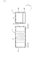
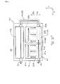
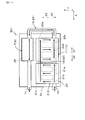
- FIG. 1 is a plan view showing an outline of the power conversion device of Embodiment 1.
- 2 is a cross-sectional view taken along line II-II in FIG.
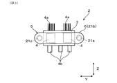
- FIG. 3 is a view of the semiconductor lamination unit in FIG. 1 as viewed from the lamination direction of the semiconductor modules
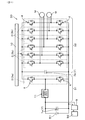
- FIG. 4 is an inverter circuit diagram of the power conversion device of the first embodiment
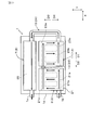
- FIG. 5 is a view schematically showing a cooling structure of the power conversion device of the first embodiment
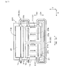
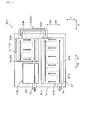
- FIG. 6 is a view schematically showing a cooling structure of the power conversion device of Embodiment 2.
- FIG. 1 is a plan view showing an outline of the power conversion device of Embodiment 1.
- 2 is a cross-sectional view taken along line II-II in FIG.
- FIG. 3 is a view of the semiconductor lamination unit in FIG. 1 as viewed from the lamination direction of the semiconductor modules
- FIG. 4 is an inverter circuit diagram of the power conversion device of the first embodiment
- FIG. 5 is a view schematic
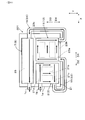
- FIG. 7 is a view schematically showing a cooling structure of the power conversion device of Embodiment 3.
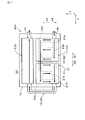
- FIG. 8 is a view schematically showing a cooling structure of the power conversion device of the fourth embodiment
- FIG. 9 is a view schematically showing a cooling structure of the power conversion device of the fifth embodiment
- FIG. 10 is a view schematically showing a cooling structure of the power conversion device of the sixth embodiment
- FIG. 11 is a view schematically showing a cooling structure of the power conversion device of the seventh embodiment.
- the stacking direction of the plurality of semiconductor modules constituting the semiconductor stacking unit is indicated by arrow X
- the orthogonal direction orthogonal to the stacking direction is indicated by arrow Y
- the stacking direction X The vertical direction (also referred to as the “height direction”) orthogonal to both of the orthogonal directions Y is indicated by an arrow Z.
- the power conversion device 1 As shown in FIG. 1, the power conversion device 1 according to the first embodiment includes a semiconductor multilayer unit 2, a plurality of reactors 11, a capacitor 7, a converter 9 (see FIG. 4), and a control circuit in a case 1 a. And the substrate 10 is accommodated.
- the power conversion device 1 is mounted, for example, on an electric car, a hybrid car, etc., and is used as an inverter for converting direct current source power into alternating current power necessary for driving a driving motor.
- stacking unit 2 mutually laminates
- the semiconductor lamination unit 2 further includes a cooler 5 having a plurality of cooling pipes 6.
- a plurality of semiconductor modules 3 and a plurality of cooling pipes 6 of the cooler 5 are alternately laminated in the lamination direction X. That is, each semiconductor module 3 is sandwiched by two cooling pipes 6 from both side surfaces in the stacking direction X.
- the number of stacked semiconductor modules 3 in the semiconductor stacked unit 2 can be appropriately set as needed.
- the semiconductor lamination unit 2 is provided with a refrigerant flow passage 21 through which the refrigerant flows.
- the refrigerant flow passage 21 is configured by an inlet header portion 21 a, a plurality of cooling portions 21 b, and an outlet header portion 21 c.
- the inlet header portion 21a is a flow path extending in the stacking direction X, and the upstream side thereof is in communication with the inflow pipe 1b, and the downstream side thereof is in communication with the inlet portions of the plurality of cooling pipes 6 There is.
- the cooling unit 21 b is configured as a flow path extending in the orthogonal direction Y between the inlet header 21 a and the outlet header 21 c.
- the outlet header portion 21c is a flow path extending in the stacking direction X in parallel with the inlet header portion 21a, and is configured to communicate with the outlet portions of the plurality of cooling pipes 6 and to communicate with the connecting pipe 14 There is.
- refrigerant flowing from the inflow pipe 1b examples include natural refrigerants such as water and ammonia, water mixed with ethylene glycol antifreeze, fluorocarbon refrigerants such as Fluorinert (registered trademark), and fluorocarbon refrigerants such as HCFC 123 and HFC 134a It is preferable to use an alcohol-based refrigerant such as methanol or alcohol, or a ketone-based refrigerant such as acetone.
- the plurality of reactors 11 are stacked in the stacking direction X with each other. That is, the reactor 11 is stacked in the same direction as the stacking direction X of the semiconductor module 3.
- Each reactor 11 is an electronic component having a function of converting electric energy into magnetic energy using an inductor, and accommodates in the case 12 a coil 13 that generates a magnetic flux when energized.
- the plurality of reactors 11 constitute an inverter circuit (an inverter circuit 30 described later) of the power conversion device 1 together with the semiconductor module 3, and more specifically, a booster circuit (step-up circuit) that boosts a DC voltage which is an input voltage to the semiconductor module 3 It comprises the below-mentioned booster 31).
- the number of reactors 11 can be appropriately set as needed.
- the plurality of reactors 11 are provided with a refrigerant flow passage 23 through which the refrigerant flows.
- the refrigerant flow passage 23 is configured by an inlet header portion 23a, a plurality of cooling portions 23b, and an outlet header portion 23c.
- the inlet header portion 23 a is a flow path extending in the stacking direction X, and is configured to communicate with the outlet header portion 21 c of the refrigerant flow passage 21 through the refrigerant flow passage 22 of the connection pipe 14.
- the cooling portion 23 b is configured as a flow path extending in the orthogonal direction Y between the inlet header portion 23 a and the outlet header portion 23 c.
- the outlet header portion 23 c is a flow path extending in the stacking direction X in parallel with the inlet header portion 23 a with the coil 13 interposed therebetween, and is configured to communicate with the inlet portion of the connection pipe 15.
- the capacitor 7 is electrically connected to the plurality of semiconductor modules 3.
- the capacitor 7 includes a capacitor 7a for removing noise current included in a current supplied from a DC power supply in a booster 31 described later, and a capacitor for smoothing a DC voltage boosted in the booster 31. And 7b are included (see FIG. 4).
- the capacitor 7a is also referred to as a filter capacitor, and the capacitor 7b is also referred to as a smoothing capacitor.
- the capacitor element 8 of the capacitors 7a and 7b is accommodated in the case 8a.
- the capacitor 7 can also be referred to as a capacitor module including the capacitor 7a and the capacitor 7b.
- the condenser 7 is provided with a refrigerant flow passage 25 through which the refrigerant flows.
- the refrigerant flow passage 25 is disposed below the condenser element 8 in the vertical direction Z (see FIG. 2).
- the structure for cooling the capacitor 7 can be simplified.
- the refrigerant flow passage 25 of the condenser 7 is configured such that the upstream side thereof communicates with the outlet of the connection pipe 15 and the downstream side thereof communicates with the outflow pipe 1c. According to this configuration, the refrigerant flowing into the refrigerant flow passage 25 through the refrigerant flow passage 24 of the connection pipe 15 flows from the outflow pipe 1c to the refrigerant flow passage 25 toward the outflow pipe 1c. At this time, the heat generated in the condenser 7 moves to the refrigerant flowing through the refrigerant flow passage 25 to cool the condenser 7.
- the plurality of reactors 11 are arranged adjacent to the semiconductor lamination unit 2 in the lamination direction X.
- the capacitor 7 extends in the stacking direction X, and is disposed opposite to both the plurality of reactors 11 and the semiconductor multilayer unit 2 in the orthogonal direction Y orthogonal to the stacking direction X with the space portion 16 therebetween. There is. For this reason, a plurality of reactors 11 and capacitors 7 are disposed adjacent to each other in the orthogonal direction Y.
- the inlet header portion 23 a constituting the refrigerant flow passage 23 for the reactor 11 is disposed to face the capacitor element 8 of the capacitor 7 across the space portion 16 in the orthogonal direction Y. It becomes a counter flow passage that has been According to such an arrangement, the capacitor element 8 is cooled by heat exchange with the refrigerant flowing through the inlet header portion 23 a on the reactor 11 side. That is, the refrigerant of the inlet header portion 23 a used to cool the coil 13 of the reactor 11 can also be used to cool the capacitor element 8 of the capacitor 7.
- the refrigerant flow passage 25 of the condenser 7 is disposed to face the plurality of reactors 11 with the space portion 16 separated in the orthogonal direction Y. According to such an arrangement, the reactor 11 is cooled by heat exchange with the refrigerant flowing in the refrigerant flow passage 25 on the condenser 7 side. That is, the refrigerant in the refrigerant flow passage 25 used to cool the capacitor element 8 of the capacitor 7 can also be used to cool the coil 13 of the reactor 11.
- the semiconductor module 3 incorporates a semiconductor element 4 such as an IGBT that converts DC power into AC power.
- the semiconductor module 3 is provided with a plurality of control terminals 4a electrically connected to the control circuit board 10, and a power terminal 4b for power supply.
- the control circuit board 10 is configured to control the switching operation of the semiconductor element 4 in order to convert direct current power supplied from the power terminal 4 b to the semiconductor module 3 into alternating current power.
- the switching operation (on / off operation) of the semiconductor element 4 built in each of the plurality of semiconductor modules 3 is controlled by the control circuit board 10,
- the DC power of the power source B1 which is a DC power source is converted into AC power.
- the plurality of semiconductor modules 3 are classified into a semiconductor module 3a and a semiconductor module 3b.
- the capacitor 7a, the reactor 11, and the semiconductor module 3a constitute a booster 31 as a booster circuit of the inverter circuit 30.
- the boosting unit 31 has a function of boosting the voltage of the power supply B1.
- the conversion part 32 of the inverter circuit 30 is comprised by the capacitor
- the converter 32 has a function of converting DC power after being boosted by the booster 31 into AC power.
- the AC power obtained by the conversion unit 32 drives a three-phase AC motor M for traveling the vehicle.
- FIG. 4 describes the case where the inverter circuit 30 includes the two conversion units 32 and accordingly the two three-phase AC motors M are driven, but instead, the number of the conversion units 32 is used. It is also possible to adopt a structure in which one three-phase AC motor M is driven accordingly.
- the converter 9 is connected to the power supply B1 and used to step down the voltage of the power supply B1 to charge the auxiliary battery B2 having a lower voltage than the power supply B1.
- the auxiliary battery B2 is used as a power supply of various devices mounted on the vehicle.
- the number and arrangement of the components constituting the above-described inverter circuit 30 are not limited to those shown in FIG. 4 and can be appropriately changed as needed.
- one of the stacking directions X is referred to as a first direction D1, and the other direction is referred to as a second direction D2.
- one of the orthogonal directions Y is referred to as a third direction D3, and the other direction is referred to as a fourth direction D4.
- stacking unit 2 is simplified and shown for convenience of explanation, and the several reactor 11 is simplified and shown as the one reactor 11.
- stacking unit 2 and the reactor 11 differs from the structure of the refrigerant
- the refrigerant flows continuously through the refrigerant path from the inflow pipe 1b to the outflow pipe 1c.
- the refrigerant flow passage 21 of the semiconductor lamination unit 2, the refrigerant flow passage 23 of the reactor 11, and the refrigerant flow passage 25 of the condenser 7 communicate with each other in the refrigerant passage.
- the refrigerant for cooling the three heat generating components can be used in common, and the structure of the refrigerant flow passage for that can be simplified.
- the refrigerant flowing from the inflow pipe 1 b first flows through the refrigerant flow passage 21 of the semiconductor lamination unit 2.
- the refrigerant flowing from the inflow pipe 1b flows in the first direction D1 while branching the inlet header portion 21a into the plurality of cooling portions 21b. Then, the refrigerant of the cooling unit 21b flows in the third direction D3 toward the outlet header 21c. At this time, the heat generated in the semiconductor module 3 moves toward the refrigerant flowing through the cooling unit 21 b, whereby the semiconductor module 3 is cooled.
- the refrigerants having flowed through the cooling unit 21b flow toward the connection pipe 14 in the first direction D1 toward the connecting pipe 14 while merging.
- the refrigerant joined at the outlet header 21 c of the refrigerant flow passage 21 flows through the refrigerant flow passage 22 of the connection pipe 14 and then flows into the refrigerant flow passage 23 of the reactor 11.
- the refrigerant flowing from the refrigerant flow passage 22 of the connection pipe 14 flows in the first direction D1 while branching the inlet header portion 23a into the plurality of cooling portions 23b. Therefore, a linear refrigerant flow in the first direction D1 is formed from the outlet header portion 21c of the refrigerant flow passage 21 to the inlet header portion 23a of the refrigerant flow passage 23 through the connection pipe 14.
- the refrigerant of the cooling unit 23b flows toward the outlet header 23c in the fourth direction D4.
- the heat generated at the coil 13 of the reactor 11 moves to the refrigerant side flowing through the cooling portion 23 b, whereby the reactor 11 is cooled.
- the refrigerant having flowed through the cooling portion 23b flows toward the connection pipe 15 in the first direction D1 toward the connection pipe 15 while merging.
- the refrigerant joined at the outlet header portion 23c of the refrigerant flow passage 23 flows through the refrigerant flow passage 24 of the connection pipe 15 to change the direction from the first direction D1 to the second direction D2, and then flows into the refrigerant flow passage 25 of the condenser 7. Do.
- the refrigerant flowing from the refrigerant flow passage 24 of the connection pipe 15 flows toward the outflow pipe 1c in the second direction D2, and then flows out from the outflow pipe 1c. At this time, the heat generated by the capacitor element 8 of the capacitor 7 moves to the refrigerant side flowing through the refrigerant flow passage 25 to cool the capacitor element 8.
- the refrigerant flowing through the refrigerant flow passage 23 of the reactor 11 has a function of cooling the reactor 11 itself.
- the function of cooling the capacitor 7 disposed adjacent to the reactor 11 is also achieved.
- the refrigerant flowing through the refrigerant flow passage 25 of the condenser 7 also functions to cool the reactor 11 disposed adjacent to the condenser 7. That is, the refrigerant flowing through one of the refrigerant flow passages of the reactor 11 and the condenser 7 also serves to cool the other.
- the semiconductor multilayer is Cooling can be performed more efficiently than in the case of cooling each of the unit 2, the reactor 11, and the condenser 7 only with the refrigerant flowing through the dedicated refrigerant flow passage. Therefore, the power converter device 1 which can improve the cooling performance with respect to heat-emitting components can be provided. In order to improve the cooling performance, it is preferable to keep the dimension in the orthogonal direction Y of the space 16 small.
- the refrigerant flow passage 25 of the capacitor 7 is disposed below the capacitor element 8, and the inlet header portion 23 a constituting the refrigerant flow passage 23 of the reactor 11 is on the side of the capacitor element 8. It is arranged facing each other. For this reason, the cooling performance to the capacitor element 8 can be enhanced by cooling the capacitor element 8 from both directions below and to the side.
- the power conversion device 101 of the second embodiment is different from that of the power conversion device 1 of the first embodiment in the structure of the refrigerant flow passage 23 of the reactor 11.
- the other configuration is the same as that of the first embodiment.
- the positions of the inlet header portion 23 a and the outlet header portion 23 c constituting the refrigerant flow passage 23 are opposite to those of the first embodiment. That is, the inlet header portion 23a is provided on the opposite side of the outlet header portion 23c to the capacitor 7.
- a linear refrigerant flow in the first direction D1 is formed from the outlet header portion 21c of the refrigerant flow passage 21 to the inlet header portion 23a of the refrigerant flow passage 23 through the connection pipe 14.
- the reactor 11 can be cooled by changing the refrigerant path in the refrigerant flow passage 23.
- Other effects and effects similar to those of the first embodiment are achieved.
- the power conversion device 201 of the third embodiment is different from that of the power conversion device 1 of the first embodiment in the respective structures of the refrigerant flow passage 21 of the stacked semiconductor unit 2, the coolant flow passage 23 of the reactor 11, and the connection pipe 14. ing.
- the other configuration is the same as that of the first embodiment.
- the positions of the inlet header portion 21 a and the outlet header portion 21 c that constitute the refrigerant flow passage 21 are opposite to those of the first embodiment. That is, the outlet header portion 21c is provided on the opposite side of the inlet header portion 21a to the capacitor 7.
- the positions of the inlet header portion 23a and the outlet header portion 23c constituting the refrigerant flow passage 23 are opposite to those in the first embodiment. That is, the inlet header portion 23a is provided on the opposite side of the outlet header portion 23c to the capacitor 7.
- connecting pipe 14 is connected at its inlet to the left end in FIG. 7 of both ends in the stacking direction X of the outlet header 21c, and its outlet is in FIG. 7 of the inlet header 23a. Connected to the right end.
- the refrigerant of the cooling unit 21b flows toward the outlet header 21c in the fourth direction D4, and the refrigerant of the outlet header 21c flows toward the inlet of the connection pipe 14 in the second direction. It flows to D2.
- the refrigerant in the inlet header 23a flows from the outlet of the connection pipe 14 in the second direction D2, and the refrigerant in the cooling unit 23b flows toward the outlet header 23c in the third direction D3. Flow.
- the path of the refrigerant in the refrigerant flow passage 21 can be changed to cool the semiconductor lamination unit 2, and the path of the refrigerant in the refrigerant flow passage 23 can be changed to change the reactor 11. Can be cooled.
- Other effects and effects similar to those of the first embodiment are achieved.
- the power conversion device 301 of the fourth embodiment is the same as the power conversion device 1 of the first embodiment in the respective structures of the refrigerant flow passage 21 of the stacked semiconductor unit 2, the reactor 11 and the refrigerant flow passage 23, the connection pipe 14 and the connection pipe 15. It is different from The other configuration is the same as that of the first embodiment.
- the positions of the inlet header portion 21 a and the outlet header portion 21 c constituting the refrigerant flow passage 21 are opposite to those of the first embodiment. That is, the outlet header portion 21c is provided on the opposite side of the inlet header portion 21a to the capacitor 7.
- the reactor 11 is stacked in the orthogonal direction Y. Therefore, in the refrigerant flow passage 23 for the reactor 11, the inlet header portion 23a and the outlet header portion 23c extend in parallel to each other in the orthogonal direction Y, and the inlet header portion 23a is disposed on the semiconductor lamination unit 2 side
- the cooling portion 23b extends in the stacking direction X between the inlet header portion 23a and the outlet header portion 23c.
- the connecting pipe 14 has its inlet connected to the left end in FIG. 8 of both ends in the stacking direction X of the outlet header 21c, and its outlet is in the orthogonal direction Y of the outlet header 23c. Among the both ends, it is connected to the lower end in FIG.
- connecting pipe 15 is connected at its inlet to the lower end in FIG. 8 of both ends in the orthogonal direction Y of the outlet header 23c.
- the refrigerant of the cooling unit 21b flows toward the outlet header 21c in the fourth direction D4, and the refrigerant of the outlet header 21c flows toward the inlet of the connection pipe 14 in the second direction. It flows to D2.
- the refrigerant in the inlet header portion 23a flows from the outlet of the connection pipe 14 in the third direction D3, and the refrigerant in the cooling portion 23b flows toward the outlet header portion 23c in the first direction D1.
- the refrigerant in the outlet header portion 23c flows toward the inlet portion of the connection pipe 15 in the fourth direction D4.
- the semiconductor lamination unit 2 can be cooled by changing the refrigerant passage in the refrigerant passage 21, and the reactor 11 laminated in the orthogonal direction Y can be used as the refrigerant passage 23.
- Embodiment 5 The power conversion device 401 of the fifth embodiment differs from the power conversion device 1 of the first embodiment in the path of the refrigerant from the inflow pipe 1 b to the outflow pipe 1 c.
- the other configuration is the same as that of the first embodiment.
- the refrigerant flowing from the inflow pipe 1 b first flows to the refrigerant flow passage 23 of the reactor 11 and then flows to the refrigerant flow passage 21 of the semiconductor lamination unit 2.
- the refrigerant flowing from the inflow pipe 1b flows in the second direction D2 while branching the inlet header portion 23a into the plurality of cooling portions 23b.
- the refrigerant of the cooling unit 23b flows in the third direction D3 toward the outlet header 23c. Then, the refrigerant flowing through the cooling unit 21b flows toward the connection pipe 14 in the second direction D2 toward the connection pipe 14 while merging.
- the refrigerant flowing from the refrigerant flow passage 22 of the connection pipe 14 flows in the second direction D2 while branching the inlet header portion 21a into the plurality of cooling portions 21b.
- the refrigerant of the cooling unit 21b flows in the fourth direction D4 toward the outlet header 21c. Then, the refrigerant flowing through the cooling unit 21b flows toward the connection pipe 15 in the second direction D2 toward the connection pipe 15 while merging.
- cooling of the reactor 11, the semiconductor multilayer unit 2, and the capacitor 7 can be performed in the order of the refrigerant path from the inflow pipe 1 b to the outflow pipe 1 c.
- Other effects and effects similar to those of the first embodiment are achieved.
- Embodiment 6 The power conversion device 501 of the sixth embodiment differs from the power conversion device 1 of the first embodiment in the arrangement of the capacitors 7.
- the other configuration is the same as that of the first embodiment.
- the capacitor 7 has a dimension in the stacking direction X, that is, a dimension in the stacking direction X of the case 8a (see FIG. 1) is shorter than that in the first embodiment. And while this capacitor
- the arrangement of the capacitor 7 with respect to the reactor 11 can be changed.
- Other effects and effects similar to those of the first embodiment are achieved.
- the power conversion device 601 of the seventh embodiment is different from that of the power conversion device 1 of the first embodiment in the arrangement of the semiconductor multilayer unit 2, the reactor 11 and the capacitor 7.
- the other configuration is the same as that of the first embodiment.
- the dimension in the stacking direction X of the semiconductor multilayer unit 2 is longer than that in the first embodiment, and the dimension in the stacking direction X of the capacitor 7 is larger than that in the first embodiment. Too short.
- the reactor 11 and the capacitor 7 are disposed adjacent to each other in the stacking direction X.
- the arrangement of each of the stacked semiconductor unit 2, the reactor 11, and the capacitor 7 can be changed. Other effects and effects similar to those of the first embodiment are achieved.
- the above embodiment exemplifies the case where the refrigerant flow passage 25 of the capacitor 7 is disposed below the capacitor element 8 in the vertical direction Z, but instead of or in addition to this, the refrigerant flow corresponding to the refrigerant flow passage 25
- the paths can also be arranged above or to the side of the capacitor element 8.
- the structure and arrangement of the refrigerant flow passage 21 in the semiconductor lamination unit 2 and the structure and arrangement of the refrigerant flow passage 23 in the reactor 11 can be changed as necessary.
Landscapes
- Engineering & Computer Science (AREA)
- Microelectronics & Electronic Packaging (AREA)
- Power Engineering (AREA)
- Physics & Mathematics (AREA)
- Thermal Sciences (AREA)
- Transportation (AREA)
- Mechanical Engineering (AREA)
- Inverter Devices (AREA)
Abstract
電力変換装置(1)は、いずれも半導体素子(4)を内蔵した複数の半導体モジュール(3)が互いに積層方向Xに積層されてなる半導体積層ユニット(2)と、直流電圧を昇圧する昇圧回路を構成するリアクトル(11)と、複数の半導体モジュール(3)に電気的に接続されたコンデンサ(7)と、を備え、半導体積層ユニット(2)とリアクトル(11)とコンデンサ(7)のそれぞれに冷媒流通路(21,23,25)が設けられており、且つリアクトル(11)とコンデンサ(7)が互いに隣接して配置されている。
Description
本出願は、2017年8月31日に出願された日本出願番号2017-167636号に基づくもので、ここにその記載内容を援用する。
本開示は、直流電力と交流電力との間で電力変換を行う電力変換装置に関する。
従来、下記の特許文献1に、電気自動車、ハイブリッド自動車等の車両に搭載される電力変換装置が開示されている。この電力変換装置は、直流電力と交流電力との間で電力変換を行うものであり、半導体素子を内蔵した複数の半導体モジュールが互いに積層されてなる半導体積層ユニットと、平滑用のコンデンサと、昇圧用のリアクトルと、を備えている。
この電力変換装置において、発熱部品である半導体積層ユニットに対しては隣接する2つの半導体モジュールの間に冷媒が流れる第1冷媒流通路が設けられている。また、別の発熱部品であるコンデンサに対しては半導体積層ユニットとの間に第1冷媒流通路に連通する第2冷媒流通路が設けられている。これにより、第1冷媒流通路を流れる冷媒によって半導体積層ユニットの各半導体モジュールが冷却され、更に第1冷媒流通路から第2冷媒流通路へと流れる冷媒によってコンデンサが冷却されるようになっている。
この種の電力変換装置の設計に際しては、上記のような電力変換装置のような半導体積層ユニット及びコンデンサの冷却のみならず、リアクトルを含めた発熱部品を効率良く冷却することによって冷却性能を向上させたいという要請がある。
本開示は、発熱部品に対する冷却性能を向上させることができる電力変換装置を提供しようとするものである。
本開示の一態様は、
いずれも半導体素子を内蔵した複数の半導体モジュールが互いに積層方向に積層されてなる半導体積層ユニットと、
直流電圧を昇圧する昇圧回路を構成するリアクトルと、
上記複数の半導体モジュールに電気的に接続されたコンデンサと、
を備え、
上記半導体積層ユニットと上記リアクトルと上記コンデンサのそれぞれに冷媒流通路が設けられており、且つ上記リアクトルと上記コンデンサが互いに隣接して配置されている、電力変換装置、
にある。
いずれも半導体素子を内蔵した複数の半導体モジュールが互いに積層方向に積層されてなる半導体積層ユニットと、
直流電圧を昇圧する昇圧回路を構成するリアクトルと、
上記複数の半導体モジュールに電気的に接続されたコンデンサと、
を備え、
上記半導体積層ユニットと上記リアクトルと上記コンデンサのそれぞれに冷媒流通路が設けられており、且つ上記リアクトルと上記コンデンサが互いに隣接して配置されている、電力変換装置、
にある。
上記の電力変換装置において、発熱部品の1つであるリアクトルの冷媒流通路を流れる冷媒は、リアクトル自体を冷却する機能に加えて、このリアクトルに隣接して配置されたコンデンサをも冷却する機能を果たす。同様に、別の発熱部品であるコンデンサの冷媒流通路を流れる冷媒は、コンデンサ自体を冷却する機能に加えて、このコンデンサに隣接して配置されたリアクトルをも冷却する機能を果たす。即ち、リアクトル及びコンデンサの一方の冷媒流通路を流れる冷媒が他方の冷却を兼務している。このため、リアクトル及びコンデンサのそれぞれを専用の冷媒流通路を流れる冷媒のみで冷却する場合に比べて効率良く冷却することができる。
以上のごとく、上記態様によれば、発熱部品に対する冷却性能を向上させることができる電力変換装置を提供できる。
なお、特許請求の範囲に記載した括弧内の符号は、後述する実施形態に記載の具体的手段との対応関係を示すものであり、本開示の技術的範囲を限定するものではない。
なお、特許請求の範囲に記載した括弧内の符号は、後述する実施形態に記載の具体的手段との対応関係を示すものであり、本開示の技術的範囲を限定するものではない。
本開示についての上記目的およびその他の目的、特徴や利点は、添付の図面を参照しながら下記の詳細な記述により、より明確になる。その図面は、
図1は、実施形態1の電力変換装置の概要を示す平面図であり、
図2は、図1のII-II線矢視断面図であり、
図3は、図1中の半導体積層ユニットを半導体モジュールの積層方向から視た図であり、
図4は、実施形態1の電力変換装置のインバータ回路図であり、
図5は、実施形態1の電力変換装置の冷却構造を模式的に示す図であり、
図6は、実施形態2の電力変換装置の冷却構造を模式的に示す図であり、
図7は、実施形態3の電力変換装置の冷却構造を模式的に示す図であり、
図8は、実施形態4の電力変換装置の冷却構造を模式的に示す図であり、
図9は、実施形態5の電力変換装置の冷却構造を模式的に示す図であり、
図10は、実施形態6の電力変換装置の冷却構造を模式的に示す図であり、
図11は、実施形態7の電力変換装置の冷却構造を模式的に示す図である。
以下、電力変換装置に係る実施形態について、図面を参照しつつ説明する。
なお、本明細書の図面では、特に断わらない限り、半導体積層ユニットを構成する複数の半導体モジュールの積層方向を矢印Xで示し、その積層方向と直交する直交方向を矢印Yで示し、積層方向X及び直交方向Yの両方に直交する上下方向(「高さ方向」ともいう。)を矢印Zで示すものとする。
(実施形態1)
図1に示されるように、実施形態1にかかる電力変換装置1は、ケース1a内に半導体積層ユニット2と、複数のリアクトル11と、コンデンサ7と、コンバータ9(図4参照)と、制御回路基板10と、を収容している。この電力変換装置1は、例えば、電気自動車やハイブリッド自動車等に搭載され、直流の電源電力を駆動用モータの駆動に必要な交流電力に変換するインバータとして用いられる。
図1に示されるように、実施形態1にかかる電力変換装置1は、ケース1a内に半導体積層ユニット2と、複数のリアクトル11と、コンデンサ7と、コンバータ9(図4参照)と、制御回路基板10と、を収容している。この電力変換装置1は、例えば、電気自動車やハイブリッド自動車等に搭載され、直流の電源電力を駆動用モータの駆動に必要な交流電力に変換するインバータとして用いられる。
半導体積層ユニット2は、いずれも半導体素子4(図3参照)を内蔵した複数の半導体モジュール3が互いに積層方向Xに積層されてなる。また、この半導体積層ユニット2は、複数の冷却管6を有する冷却器5を備えている。この半導体積層ユニット2において、複数の半導体モジュール3と冷却器5の複数の冷却管6とが積層方向Xに交互に積層配置されている。即ち、各半導体モジュール3は、2つの冷却管6によって積層方向Xの両側面から挟持されている。
なお、この半導体積層ユニット2における半導体モジュール3の積層数は必要に応じて適宜に設定することができる。
なお、この半導体積層ユニット2における半導体モジュール3の積層数は必要に応じて適宜に設定することができる。
半導体積層ユニット2には、冷媒が流通する冷媒流通路21が設けられている。この冷媒流通路21は、入口ヘッダー部21aと、複数の冷却部21bと、出口ヘッダー部21cと、によって構成されている。
入口ヘッダー部21aは、積層方向Xに延在する流路であり、その上流側が流入管1bに連通し、且つその下流側が複数の冷却管6のそれぞれの入口部分に連通するように構成されている。冷却部21bは、入口ヘッダー部21aと出口ヘッダー部21cとの間で直交方向Yに延在する流路として構成されている。出口ヘッダー部21cは、入口ヘッダー部21aと平行に積層方向Xに延在する流路であり、複数の冷却管6のそれぞれの出口部分に連通し且つ接続管14に連通するように構成されている。
流入管1bから流入する冷媒として、例えば、水やアンモニア等の自然冷媒、エチレングリコール系の不凍液を混入した水、フロリナート(登録商標)等のフッ化炭素系冷媒、HCFC123、HFC134a等のフロン系冷媒、メタノール、アルコール等のアルコール系冷媒、アセトン等のケトン系冷媒等を用いるのが好ましい。
複数のリアクトル11は、互いに積層方向Xに積層されている。即ち、リアクトル11が半導体モジュール3の積層方向Xと同方向に積層されている。各リアクトル11は、インダクタを利用して電気エネルギーを磁気エネルギーに変換する機能を有する電子部品であり、通電により磁束を発生するコイル13をケース12内に収容している。複数のリアクトル11は、半導体モジュール3とともに電力変換装置1のインバータ回路(後述のインバータ回路30)を構成し、より具体的には半導体モジュール3への入力電圧である直流電圧を昇圧する昇圧回路(後述の昇圧部31)を構成している。
なお、このリアクトル11の数は必要に応じて適宜に設定することができる。
なお、このリアクトル11の数は必要に応じて適宜に設定することができる。
複数のリアクトル11には、冷媒が流通する冷媒流通路23が設けられている。この冷媒流通路23は、入口ヘッダー部23aと、複数の冷却部23bと、出口ヘッダー部23cと、によって構成されている。
入口ヘッダー部23aは、積層方向Xに延在する流路であり、接続管14の冷媒流通路22を通じて冷媒流通路21の出口ヘッダー部21cに連通するように構成されている。冷却部23bは、入口ヘッダー部23aと出口ヘッダー部23cとの間で直交方向Yに延在する流路として構成されている。出口ヘッダー部23cは、コイル13を挟んで入口ヘッダー部23aと平行に積層方向Xに延在する流路であり、接続管15の入口部に連通するように構成されている。
コンデンサ7は、複数の半導体モジュール3に電気的に接続されている。このコンデンサ7には、後述の昇圧部31において直流電源から供給される電流に含まれるノイズ電流を除去するためのコンデンサ7aと、この昇圧部31で昇圧された直流電圧を平滑化するためのコンデンサ7bと、が含まれている(図4参照)。コンデンサ7aは、フィルタコンデンサとも称呼され、コンデンサ7bは、平滑コンデンサとも称呼される。これらのコンデンサ7a,7bのコンデンサ素子8がケース8a内に収容されている。コンデンサ7を、コンデンサ7a及びコンデンサ7bを備えたコンデンサモジュールということもできる。
このコンデンサ7には、冷媒が流通する冷媒流通路25が設けられている。この冷媒流通路25は、上下方向Zについてコンデンサ素子8の下方に配置されている(図2参照)。このため、コンデンサ7を冷却するための構造を簡素化することができる。
また、このコンデンサ7の冷媒流通路25は、その上流側が接続管15の出口部に連通し、且つその下流側が流出管1cに連通するように構成されている。本構成によれば、接続管15の冷媒流通路24を通じて冷媒流通路25に流入した冷媒は、この冷媒流通路25を流出管1cに向けて流れた後に、この流出管1cから流出する。このとき、コンデンサ7で生じた熱が冷媒流通路25を流れる冷媒側へと移動することによって、このコンデンサ7が冷却される。
上記の電力変換装置1において、複数のリアクトル11は、半導体積層ユニット2に対して積層方向Xに隣接して配置されている。また、コンデンサ7は、積層方向Xに延在しており、積層方向Xと直交する直交方向Yについて複数のリアクトル11と半導体積層ユニット2の双方に空間部16を隔てて対向して配置されている。このため、複数のリアクトル11とコンデンサ7が直交方向Yについて互いに隣接して配置されている。
図2に示されるように、リアクトル11のための冷媒流通路23を構成する入口ヘッダー部23aは、直交方向Yについて空間部16を隔ててコンデンサ7のコンデンサ素子8の側方に対向して配置された対向流通路となる。このような配置によれば、コンデンサ素子8は、リアクトル11側の入口ヘッダー部23aを流れる冷媒との間の熱交換によって冷却される。即ち、リアクトル11のコイル13の冷却に使用する入口ヘッダー部23aの冷媒を、コンデンサ7のコンデンサ素子8の冷却にも使用できる。
また、コンデンサ7の冷媒流通路25は、直交方向Yについて空間部16を隔てて複数のリアクトル11に対向して配置されている。このような配置によれば、リアクトル11は、コンデンサ7側の冷媒流通路25を流れる冷媒との間の熱交換によって冷却される。即ち、コンデンサ7のコンデンサ素子8の冷却に使用する冷媒流通路25の冷媒を、リアクトル11のコイル13の冷却にも使用できる。
図3に示されるように、半導体モジュール3は、直流電力を交流電力に変換するIGBT等の半導体素子4を内蔵している。この半導体モジュール3には、制御回路基板10に電気的に接続された複数の制御端子4aと、電力供給用のパワー端子4bと、が設けられている。制御回路基板10は、パワー端子4bから半導体モジュール3に供給された直流電力を交流電力に変換するために、半導体素子4のスイッチング動作を制御するように構成されている。
図4に示されるように、電力変換装置1のインバータ回路30において、複数の半導体モジュール3のそれぞれに内蔵されている半導体素子4のスイッチング動作(オンオフ動作)が制御回路基板10によって制御されて、直流電源である電源B1の直流電力が交流電力に変換される。複数の半導体モジュール3は、半導体モジュール3aと、半導体モジュール3bに分類される。
本実施形態では、コンデンサ7a、リアクトル11及び半導体モジュール3aによって、インバータ回路30の昇圧回路としての昇圧部31が構成されている。この昇圧部31は、電源B1の電圧を昇圧する機能を有する。
一方で、コンデンサ7b及び半導体モジュール3bによって、インバータ回路30の変換部32が構成されている。この変換部32は、昇圧部31で昇圧された後の直流電力を交流電力に変換する機能を有する。変換部32で得られた交流電力によって、車両走行用の三相交流モータMが駆動される。
図4では、説明の便宜上、この昇圧部31を1つのみ記載しているが、実際は、図1中のリアクトル11の数に応じて複数の昇圧部31が並列接続されている。また、図4では、インバータ回路30が2つの変換部32を備え、これに応じて2つの三相交流モータMが駆動される場合について記載しているが、これに代えて変換部32の数を1つにし、これに応じて1つの三相交流モータMが駆動される構造を採用することもできる。
コンバータ9は、電源B1に接続されており、この電源B1の電圧を降圧して、電源B1よりも低圧の補助バッテリB2を充電するのに用いられる。補助バッテリB2は、車両に搭載される各種機器の電源として使用される。
なお、上記のインバータ回路30を構成する各要素の数や配置については、図4に示されるものに限定されるものではなく、必要に応じて適宜に変更が可能である。
ここで、上記電力変換装置1における冷媒の流れについて図5を参照しながら説明する。この説明では、積層方向Xのうちの一方向を第1方向D1とし他方向を第2方向D2とする。また、直交方向Yのうちの一方向を第3方向D3とし他方向を第4方向D4とする。
なお、図5では、説明の便宜上、半導体積層ユニット2を簡略化して示し、複数のリアクトル11を1つのリアクトル11として簡略化して示している。このため、半導体積層ユニット2及びリアクトル11のそれぞれにおける冷媒流通路の構造が図1中の冷媒流通路の構造と異なっている。
図5に示されるように、冷媒は流入管1bから流出管1cに至るまでの冷媒の経路を連続的に流れる。この冷媒の経路において、半導体積層ユニット2の冷媒流通路21と、リアクトル11の冷媒流通路23と、コンデンサ7の冷媒流通路25が連通するように構成されている。本構成によれば、3つの発熱部品の冷却のための冷媒を兼用することができ、そのための冷媒流通路の構造を簡素化することができる。
流入管1bから流入した冷媒は、先ず半導体積層ユニット2の冷媒流通路21を流れる。
この冷媒流通路21では、流入管1bから流入した冷媒が入口ヘッダー部21aを複数の冷却部21bに分岐しながら第1方向D1へと流れる。そして、冷却部21bの冷媒は、出口ヘッダー部21cに向けて第3方向D3へと流れる。このとき、半導体モジュール3で生じた熱が冷却部21bを流れる冷媒側へと移動することによって、この半導体モジュール3が冷却される。冷却部21bを流れた冷媒は合流しながら出口ヘッダー部21cを接続管14に向けて第1方向D1へと流れる。
冷媒流通路21の出口ヘッダー部21cで合流した冷媒は、接続管14の冷媒流通路22を流れた後にリアクトル11の冷媒流通路23に流入する。
この冷媒流通路23では、接続管14の冷媒流通路22から流入した冷媒は、入口ヘッダー部23aを複数の冷却部23bに分岐しながら第1方向D1へと流れる。このため、冷媒流通路21の出口ヘッダー部21cから接続管14を通じて冷媒流通路23の入口ヘッダー部23aまで第1方向D1の直線的な冷媒流れが形成される。
そして、冷却部23bの冷媒は、出口ヘッダー部23cに向けて第4方向D4へと流れる。このとき、リアクトル11のコイル13で生じた熱が冷却部23bを流れる冷媒側へと移動することによって、このリアクトル11が冷却される。冷却部23bを流れた冷媒は合流しながら出口ヘッダー部23cを接続管15に向けて第1方向D1へと流れる。
冷媒流通路23の出口ヘッダー部23cで合流した冷媒は、接続管15の冷媒流通路24を流れて第1方向D1から第2方向D2へ方向を変えた後にコンデンサ7の冷媒流通路25に流入する。
この冷媒流通路25では、接続管15の冷媒流通路24から流入した冷媒が流出管1cに向けて第2方向D2へと流れた後、流出管1cから流出する。このとき、コンデンサ7のコンデンサ素子8で生じた熱が冷媒流通路25を流れる冷媒側へと移動することによって、このコンデンサ素子8が冷却される。
次に、実施形態1の作用効果について説明する。
上記の電力変換装置1において、リアクトル11とコンデンサ7が直交方向Yについて互いに隣接して配置されているため、リアクトル11の冷媒流通路23を流れる冷媒は、リアクトル11自体を冷却する機能に加えて、このリアクトル11に隣接して配置されたコンデンサ7をも冷却する機能を果たす。また、コンデンサ7の冷媒流通路25を流れる冷媒は、コンデンサ7自体を冷却する機能に加えて、このコンデンサ7に隣接して配置されたリアクトル11をも冷却する機能を果たす。即ち、リアクトル11及びコンデンサ7の一方の冷媒流通路を流れる冷媒が他方の冷却を兼務している。
更に、リアクトル11が半導体積層ユニット2に対して積層方向Xに隣接して配置され、コンデンサ7が直交方向Yについてリアクトル11と半導体積層ユニット2の双方に対向して配置されているため、半導体積層ユニット2、リアクトル11及びコンデンサ7のそれぞれを専用の冷媒流通路を流れる冷媒のみで冷却する場合に比べて効率良く冷却することができる。
従って、発熱部品に対する冷却性能を向上させることができる電力変換装置1を提供できる。なお、冷却性能の向上に際しては、空間部16の直交方向Yの寸法を小さく抑えるのが好ましい。
従って、発熱部品に対する冷却性能を向上させることができる電力変換装置1を提供できる。なお、冷却性能の向上に際しては、空間部16の直交方向Yの寸法を小さく抑えるのが好ましい。
また、上記の電力変換装置1において、コンデンサ7の冷媒流通路25がコンデンサ素子8の下方に配置され、且つリアクトル11の冷媒流通路23を構成する入口ヘッダー部23aがコンデンサ素子8の側方に対向して配置されている。このため、コンデンサ素子8をその下方及び側方の双方向から冷却することで、このコンデンサ素子8に対する冷却性能を高めることができる。
以下、上記の実施形態1に関連する他の実施形態について図面を参照しつつ説明する。他の実施形態において、実施形態1の要素と同一の要素には同一の符号を付しており、当該同一の要素についての説明を省略する。
(実施形態2)
実施形態2の電力変換装置101は、リアクトル11の冷媒流通路23の構造が、実施形態1の電力変換装置1のものと相違している。
その他の構成は、実施形態1と同様である。
実施形態2の電力変換装置101は、リアクトル11の冷媒流通路23の構造が、実施形態1の電力変換装置1のものと相違している。
その他の構成は、実施形態1と同様である。
図6に示されるように、実施形態2では、冷媒流通路23を構成する入口ヘッダー部23aと出口ヘッダー部23cのそれぞれの位置が実施形態1の場合と逆になっている。即ち、入口ヘッダー部23aは、出口ヘッダー部23cを挟んでコンデンサ7とは反対側に設けられている。
これにより、冷媒流通路21の出口ヘッダー部21cから接続管14を通じて冷媒流通路23の入口ヘッダー部23aまで第1方向D1の直線的な冷媒流れが形成される。
実施形態2の電力変換装置101によれば、冷媒流通路23における冷媒の経路を変更してリアクトル11を冷却することができる。
その他、実施形態1と同様の作用効果を奏する。
その他、実施形態1と同様の作用効果を奏する。
(実施形態3)
実施形態3の電力変換装置201は、半導体積層ユニット2の冷媒流通路21、リアクトル11の冷媒流通路23、接続管14のそれぞれの構造が、実施形態1の電力変換装置1のものと相違している。
その他の構成は、実施形態1と同様である。
実施形態3の電力変換装置201は、半導体積層ユニット2の冷媒流通路21、リアクトル11の冷媒流通路23、接続管14のそれぞれの構造が、実施形態1の電力変換装置1のものと相違している。
その他の構成は、実施形態1と同様である。
図7に示されるように、実施形態3では、冷媒流通路21を構成する入口ヘッダー部21aと出口ヘッダー部21cのそれぞれの位置が実施形態1の場合と逆になっている。即ち、出口ヘッダー部21cは、入口ヘッダー部21aを挟んでコンデンサ7とは反対側に設けられている。
また、冷媒流通路23を構成する入口ヘッダー部23aと出口ヘッダー部23cのそれぞれの位置が実施形態1の場合と逆になっている。即ち、入口ヘッダー部23aは、出口ヘッダー部23cを挟んでコンデンサ7とは反対側に設けられている。
更に、接続管14は、その入口部が出口ヘッダー部21cの積層方向Xの両端部のうち図7中の左側の端部に接続され、且つその出口部が入口ヘッダー部23aの図7中の右側の端部に接続されている。
これにより、冷媒流通路21においては、冷却部21bの冷媒が出口ヘッダー部21cに向けて第4方向D4へと流れ、出口ヘッダー部21cの冷媒が接続管14の入口部に向けて第2方向D2へと流れる。また、冷媒流通路23においては、入口ヘッダー部23aの冷媒が接続管14の出口部から第2方向D2へと流れ、冷却部23bの冷媒が出口ヘッダー部23cに向けて第3方向D3へと流れる。
実施形態3の電力変換装置201によれば、冷媒流通路21における冷媒の経路を変更して半導体積層ユニット2を冷却することができ、また冷媒流通路23における冷媒の経路を変更してリアクトル11を冷却することができる。
その他、実施形態1と同様の作用効果を奏する。
その他、実施形態1と同様の作用効果を奏する。
(実施形態4)
実施形態4の電力変換装置301は、半導体積層ユニット2の冷媒流通路21、リアクトル11とその冷媒流通路23、接続管14、接続管15のそれぞれの構造が、実施形態1の電力変換装置1のものと相違している。
その他の構成は、実施形態1と同様である。
実施形態4の電力変換装置301は、半導体積層ユニット2の冷媒流通路21、リアクトル11とその冷媒流通路23、接続管14、接続管15のそれぞれの構造が、実施形態1の電力変換装置1のものと相違している。
その他の構成は、実施形態1と同様である。
図8に示されるように、実施形態4では、冷媒流通路21を構成する入口ヘッダー部21aと出口ヘッダー部21cのそれぞれの位置が実施形態1の場合と逆になっている。即ち、出口ヘッダー部21cは、入口ヘッダー部21aを挟んでコンデンサ7とは反対側に設けられている。
また、リアクトル11は直交方向Yに積層されている。このため、リアクトル11のための冷媒流通路23において、入口ヘッダー部23a及び出口ヘッダー部23cは、直交方向Yに互いに平行に延在し且つ入口ヘッダー部23aが半導体積層ユニット2側に配置されており、且つ冷却部23bは、入口ヘッダー部23aと出口ヘッダー部23cとの間で積層方向Xに延在している。
また、接続管14は、その入口部が出口ヘッダー部21cの積層方向Xの両端部のうち図8中の左側の端部に接続され、且つその出口部が出口ヘッダー部23cの直交方向Yの両端部のうち図8中の下側の端部に接続されている。
更に、接続管15は、その入口部が出口ヘッダー部23cの直交方向Yの両端部のうち図8中の下側の端部に接続されている。
これにより、冷媒流通路21においては、冷却部21bの冷媒が出口ヘッダー部21cに向けて第4方向D4へと流れ、出口ヘッダー部21cの冷媒が接続管14の入口部に向けて第2方向D2へと流れる。また、冷媒流通路23においては、入口ヘッダー部23aの冷媒が接続管14の出口部から第3方向D3へと流れ、冷却部23bの冷媒が出口ヘッダー部23cに向けて第1方向D1へと流れ、出口ヘッダー部23cの冷媒が接続管15の入口部に向けて第4方向D4へと流れる。
実施形態4の電力変換装置301によれば、冷媒流通路21における冷媒の経路を変更して半導体積層ユニット2を冷却することができ、また直交方向Yに積層されたリアクトル11を冷媒流通路23の冷媒で冷却することができる。
その他、実施形態1と同様の作用効果を奏する。
その他、実施形態1と同様の作用効果を奏する。
(実施形態5)
実施形態5の電力変換装置401は、流入管1bから流出管1cに至るまでの冷媒の経路が実施形態1の電力変換装置1のものと相違している。
その他の構成は、実施形態1と同様である。
実施形態5の電力変換装置401は、流入管1bから流出管1cに至るまでの冷媒の経路が実施形態1の電力変換装置1のものと相違している。
その他の構成は、実施形態1と同様である。
図9に示されるように、実施形態5では、流入管1bから流入した冷媒は、先ずリアクトル11の冷媒流通路23に流れ、その後に半導体積層ユニット2の冷媒流通路21に流れる。
冷媒流通路23では、流入管1bから流入した冷媒が入口ヘッダー部23aを複数の冷却部23bに分岐しながら第2方向D2へと流れる。また、冷却部23bの冷媒は、出口ヘッダー部23cに向けて第3方向D3へと流れる。そして、冷却部21bを流れた冷媒は合流しながら出口ヘッダー部23cを接続管14に向けて第2方向D2へと流れる。
冷媒流通路21では、接続管14の冷媒流通路22から流入した冷媒は、入口ヘッダー部21aを複数の冷却部21bに分岐しながら第2方向D2へと流れる。また、冷却部21bの冷媒は、出口ヘッダー部21cに向けて第4方向D4へと流れる。そして、冷却部21bを流れた冷媒は合流しながら出口ヘッダー部21cを接続管15に向けて第2方向D2へと流れる。
実施形態5の電力変換装置401によれば、流入管1bから流出管1cに至るまでの冷媒の経路において、リアクトル11、半導体積層ユニット2、コンデンサ7の順番での冷却が可能になる。
その他、実施形態1と同様の作用効果を奏する。
その他、実施形態1と同様の作用効果を奏する。
(実施形態6)
実施形態6の電力変換装置501は、コンデンサ7の配置が実施形態1の電力変換装置1のものと相違している。
その他の構成は、実施形態1と同様である。
実施形態6の電力変換装置501は、コンデンサ7の配置が実施形態1の電力変換装置1のものと相違している。
その他の構成は、実施形態1と同様である。
図10に示されるように、実施形態6では、コンデンサ7は、積層方向Xの寸法が、即ちケース8a(図1参照)の積層方向Xの寸法が実施形態1の場合よりも短い。そして、このコンデンサ7は、直交方向Yについてリアクトル11に空間部16を隔てて対向して配置されている一方で、半導体積層ユニット2には対向していない。
実施形態6の電力変換装置501によれば、リアクトル11に対するコンデンサ7の配置を変更することができる。
その他、実施形態1と同様の作用効果を奏する。
その他、実施形態1と同様の作用効果を奏する。
(実施形態7)
実施形態7の電力変換装置601は、半導体積層ユニット2、リアクトル11及びコンデンサ7のそれぞれの配置が実施形態1の電力変換装置1のものと相違している。
その他の構成は、実施形態1と同様である。
実施形態7の電力変換装置601は、半導体積層ユニット2、リアクトル11及びコンデンサ7のそれぞれの配置が実施形態1の電力変換装置1のものと相違している。
その他の構成は、実施形態1と同様である。
図11に示されるように、実施形態7では、半導体積層ユニット2は、積層方向Xの寸法が実施形態1の場合よりも長く、コンデンサ7は、積層方向Xの寸法が実施形態1の場合よりも短い。そして、リアクトル11とコンデンサ7が積層方向Xについて互いに隣接して配置されている。
実施形態7の電力変換装置601によれば、半導体積層ユニット2、リアクトル11及びコンデンサ7のそれぞれの配置を変更することができる。
その他、実施形態1と同様の作用効果を奏する。
その他、実施形態1と同様の作用効果を奏する。
本開示は、実施例に準拠して記述されたが、本開示は当該実施例や構造に限定されるものではないと理解される。本開示は、様々な変形例や均等範囲内の変形をも包含する。加えて、様々な組み合わせや形態、さらには、それらに一要素のみ、それ以上、あるいはそれ以下、を含む他の組み合わせや形態をも、本開示の範疇や思想範囲に入るものである。
上記の実施形態では、リアクトル11とコンデンサ7が積層方向Xや直交方向Yについて互いに隣接して配置される場合について例示したが、これに代えて、リアクトル11とコンデンサ7が上下方向Zについて互いに隣接して配置される構造を採用することもできる。
上記の実施形態では、コンデンサ7の冷媒流通路25が上下方向Zについてコンデンサ素子8の下方に配置される場合について例示したが、これに代えて或いは加えて、冷媒流通路25に相当する冷媒流通路をコンデンサ素子8の上方や側方に配置することもできる。
上記の実施形態では、半導体積層ユニット2とリアクトル11とコンデンサ7のそれぞれの冷媒流通路が連通している場合について例示したが、これに代えて、これら3つの発熱部品の全ての冷媒流通路が連通していない構造や、いずれか2つの発熱部品の冷媒流通路のみが連通している構造を採用することもできる。
上記の実施形態において、半導体積層ユニット2における冷媒流通路21の構造や配置、リアクトル11における冷媒流通路23の構造や配置を、必要に応じて変更することもできる。
Claims (4)
- いずれも半導体素子(4)を内蔵した複数の半導体モジュール(3)が互いに積層方向(X)に積層されてなる半導体積層ユニット(2)と、
直流電圧を昇圧する昇圧回路(31)を構成するリアクトル(11)と、
上記複数の半導体モジュールに電気的に接続されたコンデンサ(7)と、
を備え、
上記半導体積層ユニットと上記リアクトルと上記コンデンサのそれぞれに冷媒流通路(21,23,25)が設けられており、且つ上記リアクトルと上記コンデンサが互いに隣接して配置されている、電力変換装置(1,101,201,301,401,501,601)。 - 上記リアクトルは、上記半導体積層ユニットに対して上記積層方向に隣接して配置され、上記コンデンサは、上記積層方向と直交する直交方向(Y)について上記リアクトルと上記半導体積層ユニットの双方に対向して配置されている、請求項1に記載の電力変換装置(1,101,201,301,401)。
- 上記コンデンサの上記冷媒流通路がコンデンサ素子(8)の下方に配置され、且つ上記リアクトルの上記冷媒流通路は上記コンデンサ素子に対向して配置された対向流通路(23a)を有する、請求項1または2に記載の電力変換装置(1,101,201,301,401)。
- 上記半導体積層ユニットと上記リアクトルと上記コンデンサのそれぞれの上記冷媒流通路が連通している、請求項1~3のいずれか一項に記載の電力変換装置(1,101,201,301,401,501,601)。
Priority Applications (3)
| Application Number | Priority Date | Filing Date | Title |
|---|---|---|---|
| DE112018004851.9T DE112018004851T5 (de) | 2017-08-31 | 2018-08-30 | Leistungsumwandlungsvorrichtung |
| CN201880056174.6A CN111052585B (zh) | 2017-08-31 | 2018-08-30 | 电力转换装置 |
| US16/806,309 US11183949B2 (en) | 2017-08-31 | 2020-03-02 | Power conversion device with a coolant passage |
Applications Claiming Priority (2)
| Application Number | Priority Date | Filing Date | Title |
|---|---|---|---|
| JP2017167636A JP6724876B2 (ja) | 2017-08-31 | 2017-08-31 | 電力変換装置 |
| JP2017-167636 | 2017-08-31 |
Related Child Applications (1)
| Application Number | Title | Priority Date | Filing Date |
|---|---|---|---|
| US16/806,309 Continuation US11183949B2 (en) | 2017-08-31 | 2020-03-02 | Power conversion device with a coolant passage |
Publications (1)
| Publication Number | Publication Date |
|---|---|
| WO2019044948A1 true WO2019044948A1 (ja) | 2019-03-07 |
Family
ID=65527538
Family Applications (1)
| Application Number | Title | Priority Date | Filing Date |
|---|---|---|---|
| PCT/JP2018/032058 Ceased WO2019044948A1 (ja) | 2017-08-31 | 2018-08-30 | 電力変換装置 |
Country Status (5)
| Country | Link |
|---|---|
| US (1) | US11183949B2 (ja) |
| JP (1) | JP6724876B2 (ja) |
| CN (1) | CN111052585B (ja) |
| DE (1) | DE112018004851T5 (ja) |
| WO (1) | WO2019044948A1 (ja) |
Cited By (1)
| Publication number | Priority date | Publication date | Assignee | Title |
|---|---|---|---|---|
| JP2020150788A (ja) * | 2019-03-11 | 2020-09-17 | 株式会社デンソー | 電力変換ユニット |
Families Citing this family (3)
| Publication number | Priority date | Publication date | Assignee | Title |
|---|---|---|---|---|
| JP6758264B2 (ja) * | 2017-08-10 | 2020-09-23 | 株式会社デンソー | リアクトル冷却構造 |
| JP7433748B2 (ja) * | 2018-05-31 | 2024-02-20 | 矢崎総業株式会社 | 給電ユニット |
| JP2022160271A (ja) * | 2021-04-06 | 2022-10-19 | 三菱重工業株式会社 | 筐体及び電力変換装置 |
Citations (7)
| Publication number | Priority date | Publication date | Assignee | Title |
|---|---|---|---|---|
| JP2012217316A (ja) * | 2011-03-29 | 2012-11-08 | Denso Corp | 電力変換装置 |
| JP2012222943A (ja) * | 2011-04-07 | 2012-11-12 | Denso Corp | 電力変換装置 |
| JP2014138445A (ja) * | 2013-01-15 | 2014-07-28 | Toyota Motor Corp | 電力変換装置 |
| JP2015042131A (ja) * | 2013-08-23 | 2015-03-02 | 株式会社デンソー | 電力変換装置 |
| JP2015136223A (ja) * | 2014-01-16 | 2015-07-27 | トヨタ自動車株式会社 | 電力変換器 |
| JP2016039699A (ja) * | 2014-08-07 | 2016-03-22 | 株式会社デンソー | 電力変換装置 |
| JP2017108593A (ja) * | 2015-12-11 | 2017-06-15 | トヨタ自動車株式会社 | 封止構造 |
Family Cites Families (9)
| Publication number | Priority date | Publication date | Assignee | Title |
|---|---|---|---|---|
| JP4708459B2 (ja) * | 2008-07-29 | 2011-06-22 | 日立オートモティブシステムズ株式会社 | 電力変換装置 |
| JP4700093B2 (ja) * | 2008-10-03 | 2011-06-15 | 株式会社日立製作所 | 電子装置 |
| US8169780B2 (en) * | 2009-06-18 | 2012-05-01 | Honda Motor Co., Ltd. | Power conversion device |
| JP5799843B2 (ja) * | 2011-03-30 | 2015-10-28 | 株式会社デンソー | 電力変換装置 |
| JP5821890B2 (ja) * | 2013-04-17 | 2015-11-24 | トヨタ自動車株式会社 | 電力変換装置 |
| JP6180857B2 (ja) | 2013-09-06 | 2017-08-16 | 日立オートモティブシステムズ株式会社 | 電力変換装置 |
| JP6582783B2 (ja) * | 2015-09-16 | 2019-10-02 | 富士電機株式会社 | 半導体装置 |
| JP6500756B2 (ja) * | 2015-11-17 | 2019-04-17 | 株式会社デンソー | 電力変換装置 |
| JP6834152B2 (ja) | 2016-03-14 | 2021-02-24 | 株式会社リコー | 会議室予約装置、会議室予約方法、及びプログラム |
-
2017
- 2017-08-31 JP JP2017167636A patent/JP6724876B2/ja active Active
-
2018
- 2018-08-30 CN CN201880056174.6A patent/CN111052585B/zh active Active
- 2018-08-30 DE DE112018004851.9T patent/DE112018004851T5/de not_active Withdrawn
- 2018-08-30 WO PCT/JP2018/032058 patent/WO2019044948A1/ja not_active Ceased
-
2020
- 2020-03-02 US US16/806,309 patent/US11183949B2/en active Active
Patent Citations (7)
| Publication number | Priority date | Publication date | Assignee | Title |
|---|---|---|---|---|
| JP2012217316A (ja) * | 2011-03-29 | 2012-11-08 | Denso Corp | 電力変換装置 |
| JP2012222943A (ja) * | 2011-04-07 | 2012-11-12 | Denso Corp | 電力変換装置 |
| JP2014138445A (ja) * | 2013-01-15 | 2014-07-28 | Toyota Motor Corp | 電力変換装置 |
| JP2015042131A (ja) * | 2013-08-23 | 2015-03-02 | 株式会社デンソー | 電力変換装置 |
| JP2015136223A (ja) * | 2014-01-16 | 2015-07-27 | トヨタ自動車株式会社 | 電力変換器 |
| JP2016039699A (ja) * | 2014-08-07 | 2016-03-22 | 株式会社デンソー | 電力変換装置 |
| JP2017108593A (ja) * | 2015-12-11 | 2017-06-15 | トヨタ自動車株式会社 | 封止構造 |
Cited By (2)
| Publication number | Priority date | Publication date | Assignee | Title |
|---|---|---|---|---|
| JP2020150788A (ja) * | 2019-03-11 | 2020-09-17 | 株式会社デンソー | 電力変換ユニット |
| JP7306297B2 (ja) | 2019-03-11 | 2023-07-11 | 株式会社デンソー | 電力変換ユニット |
Also Published As
| Publication number | Publication date |
|---|---|
| CN111052585B (zh) | 2023-01-10 |
| DE112018004851T5 (de) | 2020-06-10 |
| US20200204085A1 (en) | 2020-06-25 |
| CN111052585A (zh) | 2020-04-21 |
| JP6724876B2 (ja) | 2020-07-15 |
| JP2019047607A (ja) | 2019-03-22 |
| US11183949B2 (en) | 2021-11-23 |
Similar Documents
| Publication | Publication Date | Title |
|---|---|---|
| JP2017152612A (ja) | 電力変換装置 | |
| JP5423877B2 (ja) | 積層型冷却器 | |
| JP5326334B2 (ja) | パワーコントロールユニット | |
| JP5167728B2 (ja) | 電力変換装置 | |
| JP6136760B2 (ja) | 電力変換装置 | |
| JP2017112768A (ja) | 電力変換装置 | |
| JP2014138445A (ja) | 電力変換装置 | |
| JP4600428B2 (ja) | 駆動装置一体型電力変換装置 | |
| WO2019044948A1 (ja) | 電力変換装置 | |
| JP2014212601A (ja) | 電力変換装置 | |
| JP6036585B2 (ja) | 電力変換装置 | |
| JP2015139299A (ja) | 電力変換器 | |
| JP2019036609A (ja) | リアクトル冷却構造 | |
| JP2015136223A (ja) | 電力変換器 | |
| JP6233183B2 (ja) | パワーコントロールユニット | |
| JP2016163478A (ja) | 電力変換器 | |
| JP7363261B2 (ja) | 電力変換装置 | |
| CN103687441A (zh) | 带有足够精确测定的热交换器的冷却回路 | |
| JP2018042311A (ja) | 電力変換装置 | |
| JP6943212B2 (ja) | 電力変換器 | |
| JP6631459B2 (ja) | 電力変換装置 | |
| JP6451379B2 (ja) | 電力変換装置 | |
| JP7163778B2 (ja) | 半導体装置 | |
| JP2013121236A (ja) | 電力変換装置 | |
| JP6439523B2 (ja) | 電力変換装置 |
Legal Events
| Date | Code | Title | Description |
|---|---|---|---|
| 121 | Ep: the epo has been informed by wipo that ep was designated in this application |
Ref document number: 18852086 Country of ref document: EP Kind code of ref document: A1 |
|
| 122 | Ep: pct application non-entry in european phase |
Ref document number: 18852086 Country of ref document: EP Kind code of ref document: A1 |