WO2019044783A1 - Connexion de fil supraconducteur à haute température - Google Patents
Connexion de fil supraconducteur à haute température Download PDFInfo
- Publication number
- WO2019044783A1 WO2019044783A1 PCT/JP2018/031617 JP2018031617W WO2019044783A1 WO 2019044783 A1 WO2019044783 A1 WO 2019044783A1 JP 2018031617 W JP2018031617 W JP 2018031617W WO 2019044783 A1 WO2019044783 A1 WO 2019044783A1
- Authority
- WO
- WIPO (PCT)
- Prior art keywords
- wire
- high temperature
- temperature superconducting
- wires
- bulk
- Prior art date
Links
- 239000002887 superconductor Substances 0.000 title abstract description 10
- 238000011144 upstream manufacturing Methods 0.000 claims abstract description 8
- 230000007423 decrease Effects 0.000 abstract description 5
- 239000010410 layer Substances 0.000 description 42
- 238000000034 method Methods 0.000 description 33
- 238000002844 melting Methods 0.000 description 21
- 230000008018 melting Effects 0.000 description 21
- 229910052761 rare earth metal Inorganic materials 0.000 description 17
- 238000010438 heat treatment Methods 0.000 description 16
- 239000000463 material Substances 0.000 description 15
- 239000013078 crystal Substances 0.000 description 10
- 239000000155 melt Substances 0.000 description 10
- 150000002910 rare earth metals Chemical class 0.000 description 10
- 238000009792 diffusion process Methods 0.000 description 8
- QVGXLLKOCUKJST-UHFFFAOYSA-N atomic oxygen Chemical compound [O] QVGXLLKOCUKJST-UHFFFAOYSA-N 0.000 description 7
- 238000002474 experimental method Methods 0.000 description 7
- 239000001301 oxygen Substances 0.000 description 7
- 229910052760 oxygen Inorganic materials 0.000 description 7
- 239000010949 copper Substances 0.000 description 6
- 230000006641 stabilisation Effects 0.000 description 6
- 238000011105 stabilization Methods 0.000 description 6
- 239000000758 substrate Substances 0.000 description 6
- 230000006866 deterioration Effects 0.000 description 5
- 238000010304 firing Methods 0.000 description 5
- 229910052727 yttrium Inorganic materials 0.000 description 5
- IJGRMHOSHXDMSA-UHFFFAOYSA-N Atomic nitrogen Chemical compound N#N IJGRMHOSHXDMSA-UHFFFAOYSA-N 0.000 description 4
- 229910052688 Gadolinium Inorganic materials 0.000 description 4
- BQCADISMDOOEFD-UHFFFAOYSA-N Silver Chemical compound [Ag] BQCADISMDOOEFD-UHFFFAOYSA-N 0.000 description 4
- 238000002595 magnetic resonance imaging Methods 0.000 description 4
- 229910052709 silver Inorganic materials 0.000 description 4
- 239000004332 silver Substances 0.000 description 4
- RYGMFSIKBFXOCR-UHFFFAOYSA-N Copper Chemical compound [Cu] RYGMFSIKBFXOCR-UHFFFAOYSA-N 0.000 description 3
- 229910052691 Erbium Inorganic materials 0.000 description 3
- 229910052689 Holmium Inorganic materials 0.000 description 3
- 238000005481 NMR spectroscopy Methods 0.000 description 3
- 229910052769 Ytterbium Inorganic materials 0.000 description 3
- 239000004020 conductor Substances 0.000 description 3
- 229910052802 copper Inorganic materials 0.000 description 3
- 238000011161 development Methods 0.000 description 3
- 238000004519 manufacturing process Methods 0.000 description 3
- 241000954177 Bangana ariza Species 0.000 description 2
- 229910052684 Cerium Inorganic materials 0.000 description 2
- 229910052692 Dysprosium Inorganic materials 0.000 description 2
- 229910052693 Europium Inorganic materials 0.000 description 2
- 229910052765 Lutetium Inorganic materials 0.000 description 2
- 229910052779 Neodymium Inorganic materials 0.000 description 2
- 229910052777 Praseodymium Inorganic materials 0.000 description 2
- 229910052772 Samarium Inorganic materials 0.000 description 2
- 229910052771 Terbium Inorganic materials 0.000 description 2
- 229910052775 Thulium Inorganic materials 0.000 description 2
- 238000010586 diagram Methods 0.000 description 2
- 229910052746 lanthanum Inorganic materials 0.000 description 2
- 239000007788 liquid Substances 0.000 description 2
- 229910052757 nitrogen Inorganic materials 0.000 description 2
- 238000002360 preparation method Methods 0.000 description 2
- 239000011241 protective layer Substances 0.000 description 2
- 229910052706 scandium Inorganic materials 0.000 description 2
- 238000005476 soldering Methods 0.000 description 2
- 239000007790 solid phase Substances 0.000 description 2
- 239000000126 substance Substances 0.000 description 2
- 229910001316 Ag alloy Inorganic materials 0.000 description 1
- 229910003097 YBa2Cu3O7−δ Inorganic materials 0.000 description 1
- 238000013459 approach Methods 0.000 description 1
- 238000012769 bulk production Methods 0.000 description 1
- 238000001354 calcination Methods 0.000 description 1
- 238000004364 calculation method Methods 0.000 description 1
- 230000015556 catabolic process Effects 0.000 description 1
- 239000000919 ceramic Substances 0.000 description 1
- 239000002131 composite material Substances 0.000 description 1
- 238000005336 cracking Methods 0.000 description 1
- 230000003247 decreasing effect Effects 0.000 description 1
- 238000006731 degradation reaction Methods 0.000 description 1
- 238000005516 engineering process Methods 0.000 description 1
- 239000012212 insulator Substances 0.000 description 1
- 229910052742 iron Inorganic materials 0.000 description 1
- 238000005304 joining Methods 0.000 description 1
- 239000007791 liquid phase Substances 0.000 description 1
- 238000005259 measurement Methods 0.000 description 1
- 239000007769 metal material Substances 0.000 description 1
- 239000000203 mixture Substances 0.000 description 1
- 229910052759 nickel Inorganic materials 0.000 description 1
- -1 organic acid salt Chemical class 0.000 description 1
- 238000003825 pressing Methods 0.000 description 1
- 238000012545 processing Methods 0.000 description 1
- 238000010791 quenching Methods 0.000 description 1
- 230000000171 quenching effect Effects 0.000 description 1
- 230000002787 reinforcement Effects 0.000 description 1
- 238000011160 research Methods 0.000 description 1
- 238000012827 research and development Methods 0.000 description 1
- 238000005245 sintering Methods 0.000 description 1
- 238000010583 slow cooling Methods 0.000 description 1
- 229910000679 solder Inorganic materials 0.000 description 1
- 230000035882 stress Effects 0.000 description 1
- 230000008646 thermal stress Effects 0.000 description 1
- 229910052721 tungsten Inorganic materials 0.000 description 1
Images


Classifications
-
- H—ELECTRICITY
- H01—ELECTRIC ELEMENTS
- H01R—ELECTRICALLY-CONDUCTIVE CONNECTIONS; STRUCTURAL ASSOCIATIONS OF A PLURALITY OF MUTUALLY-INSULATED ELECTRICAL CONNECTING ELEMENTS; COUPLING DEVICES; CURRENT COLLECTORS
- H01R4/00—Electrically-conductive connections between two or more conductive members in direct contact, i.e. touching one another; Means for effecting or maintaining such contact; Electrically-conductive connections having two or more spaced connecting locations for conductors and using contact members penetrating insulation
- H01R4/58—Electrically-conductive connections between two or more conductive members in direct contact, i.e. touching one another; Means for effecting or maintaining such contact; Electrically-conductive connections having two or more spaced connecting locations for conductors and using contact members penetrating insulation characterised by the form or material of the contacting members
- H01R4/68—Connections to or between superconductive connectors
-
- H—ELECTRICITY
- H01—ELECTRIC ELEMENTS
- H01B—CABLES; CONDUCTORS; INSULATORS; SELECTION OF MATERIALS FOR THEIR CONDUCTIVE, INSULATING OR DIELECTRIC PROPERTIES
- H01B12/00—Superconductive or hyperconductive conductors, cables, or transmission lines
- H01B12/02—Superconductive or hyperconductive conductors, cables, or transmission lines characterised by their form
- H01B12/06—Films or wires on bases or cores
-
- H—ELECTRICITY
- H01—ELECTRIC ELEMENTS
- H01R—ELECTRICALLY-CONDUCTIVE CONNECTIONS; STRUCTURAL ASSOCIATIONS OF A PLURALITY OF MUTUALLY-INSULATED ELECTRICAL CONNECTING ELEMENTS; COUPLING DEVICES; CURRENT COLLECTORS
- H01R4/00—Electrically-conductive connections between two or more conductive members in direct contact, i.e. touching one another; Means for effecting or maintaining such contact; Electrically-conductive connections having two or more spaced connecting locations for conductors and using contact members penetrating insulation
- H01R4/02—Soldered or welded connections
- H01R4/021—Soldered or welded connections between two or more cables or wires
-
- H—ELECTRICITY
- H10—SEMICONDUCTOR DEVICES; ELECTRIC SOLID-STATE DEVICES NOT OTHERWISE PROVIDED FOR
- H10N—ELECTRIC SOLID-STATE DEVICES NOT OTHERWISE PROVIDED FOR
- H10N60/00—Superconducting devices
- H10N60/20—Permanent superconducting devices
- H10N60/203—Permanent superconducting devices comprising high-Tc ceramic materials
-
- H—ELECTRICITY
- H10—SEMICONDUCTOR DEVICES; ELECTRIC SOLID-STATE DEVICES NOT OTHERWISE PROVIDED FOR
- H10N—ELECTRIC SOLID-STATE DEVICES NOT OTHERWISE PROVIDED FOR
- H10N60/00—Superconducting devices
- H10N60/80—Constructional details
-
- H—ELECTRICITY
- H01—ELECTRIC ELEMENTS
- H01F—MAGNETS; INDUCTANCES; TRANSFORMERS; SELECTION OF MATERIALS FOR THEIR MAGNETIC PROPERTIES
- H01F6/00—Superconducting magnets; Superconducting coils
- H01F6/06—Coils, e.g. winding, insulating, terminating or casing arrangements therefor
-
- Y—GENERAL TAGGING OF NEW TECHNOLOGICAL DEVELOPMENTS; GENERAL TAGGING OF CROSS-SECTIONAL TECHNOLOGIES SPANNING OVER SEVERAL SECTIONS OF THE IPC; TECHNICAL SUBJECTS COVERED BY FORMER USPC CROSS-REFERENCE ART COLLECTIONS [XRACs] AND DIGESTS
- Y02—TECHNOLOGIES OR APPLICATIONS FOR MITIGATION OR ADAPTATION AGAINST CLIMATE CHANGE
- Y02E—REDUCTION OF GREENHOUSE GAS [GHG] EMISSIONS, RELATED TO ENERGY GENERATION, TRANSMISSION OR DISTRIBUTION
- Y02E40/00—Technologies for an efficient electrical power generation, transmission or distribution
- Y02E40/60—Superconducting electric elements or equipment; Power systems integrating superconducting elements or equipment
Definitions
- the present invention relates to a connection of high temperature superconducting wires.
- Superconducting wires are widely used in NMR (Nuclear Magnetic Resonance) devices, MRI (Magnetic Resonance Imaging) devices, and the like.
- NMR Nuclear Magnetic Resonance
- MRI Magnetic Resonance Imaging
- high-temperature superconducting wires (REBCO superconducting wires) of a rare earth system have been produced, and research and development using this have been conducted.
- connection between the superconducting wires is an indispensable technical issue for lengthening of the wires and realization of a permanent current mode.
- the low resistance connection between REBCO superconducting wires is conventionally performed by soldering, and it is known that this method generates an electrical resistance value of about 10 ⁇ 8 ⁇ .
- Patent Document 1 proposes a method called a melt diffusion method.
- the protective layer of the two REBCO superconducting wires is removed, and the thickness of the superconducting layer brought into contact by heating to the melting point of the superconducting layer while pressing the superconducting layers into contact with each other.
- the superconducting wires are joined together by melting and diffusing a part of the direction. It is reported that this enables the REBCO superconducting wires to be connected with lower resistance than the connection by soldering.
- Patent Documents 2-3 proposes a method called a melt diffusion method.
- connection method melting method of the high temperature superconducting wire connection indirectly via a high temperature superconducting bulk body in Patent Document 4 and Non-Patent Document 1.
- This method is a method of connecting the high temperature superconducting layer and the high temperature superconductor bulk by melting the high temperature superconductor bulk and crystal-growing the high temperature superconductor layer as a seed crystal.
- This method has an advantage that connection can be performed in a short time as compared with the melt diffusion method, and the mechanical strength of the connection is strong.
- the biggest technical issue is to increase the current capacity of the superconducting connection. So far, the bulk bonding method has not so much current capacity. In addition, in the melt diffusion method, a long heat treatment of one week or more is required to increase the current capacity.
- the present invention aims to provide a technology capable of manufacturing a connection of a large current capacity in the connection of a high temperature superconducting wire.
- the present invention when connecting high temperature superconductivity wire rods, these wires are connected in a plurality of joined parts which separated mutually. More specifically, the present invention is a connecting body of high temperature superconducting wires in which high temperature superconducting wires including a high temperature superconducting layer are connected to each other, and the first high temperature superconducting wire and the second high temperature facing each other It is characterized in that the superconducting wire is connected at a plurality of junctions separated from each other along the longitudinal direction of the first high temperature superconducting wire and the second high temperature superconducting wire.
- each of the plurality of bonding points may be any of a rectangle, a rounded rectangle, and an ellipse, and the length in the longitudinal direction of the high-temperature superconducting wire is L and the length in the width direction is W It is preferable that the condition of 0.1 ⁇ L / W ⁇ 1.5 is satisfied. In addition, it is more desirable to satisfy 0.25 ⁇ L / W ⁇ 0.75.
- W and / or L for the plurality of bonding points monotonously increase from the upstream side to the downstream side along the longitudinal direction of the high-temperature superconducting wire.
- FIG. 1 (A) to 1 (C) are diagrams showing an outline of a connecting body of a superconducting wire according to an embodiment.
- FIG. 2 is a view showing the structure of a general high temperature superconducting wire.
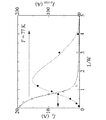
- Figure 3 is a graph showing the ratio of the length L and width W of the connecting member, a relationship between the current capacity I c-max of the joint surface current capacity I c and wire only.
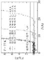
- FIG. 4 is a graph showing the measurement results of the electrical resistance when the number of junctions is one to three.
- FIG. 5 is a diagram for explaining the current flowing through the wire when the width W of the bonding portion is smaller than the wire width Ww.
- FIG. 6 is a view showing an outline of a connector in the third embodiment.
- FIG. 1 (A) is a side view of the connection of the high temperature superconducting wire
- FIG. 1 (B) is a top view of the connection of the high temperature superconducting wire
- FIG. 1C is a schematic view showing the flow of current in the high temperature superconducting wire.
- connection body of the high temperature superconducting wire material in the present embodiment is formed by connecting two high temperature superconducting wire materials 11 and 12 via a plurality of high temperature superconducting bulk bodies 13a, 13b, 13c and 13d.
- the high temperature superconducting wire may be referred to as a wire
- the high temperature superconducting bulk may be referred to as a bulk to simplify the description.
- bulk body 13a, 13b, 13c, 13d may be generically named the bulk body 13.
- the wires 11 and 12 are, for example, REBCO wires, and the bulk body 13 is a REBCO bulk having a melting point lower than that of the wires 11 and 12.
- the REBCO layer is exposed from the REBCO wire, a bulk 13 is placed between the wires, and heat treatment is performed to form a bond. Specific bonding methods are described in Non-Patent Document 1 and Patent Document 4.
- a plurality of junctions by the bulk body 13 are provided in parallel.
- the number may be any number as long as it is two or more.
- superconducting wires for NMR and MRI applications are required to have a junction current of about 100 amps (77 Kelvin & no magnetic field).
- about 10 amps (77 Kelvin & no magnetic field) is considered to be the limit that can flow in a single junction.
- the current capacity can be increased to 100 amperes by setting the number of junctions to ten.
- the wires 11 and 12 are connected via the bulk body 13 by the melt growth method has been described as an example, but the wires 11 and 12 may be directly connected by the melt diffusion method or the solid phase diffusion method. .
- the same principle as described above it is possible to significantly increase the current capacity which can be flowed throughout the connection.
- the two high temperature superconducting wires 11 and 12 are connected via the bulk body 13.
- the high temperature superconducting wires 11 and 12 are REBCO wires
- the bulk body 13 is a REBCO bulk body having a melting point lower than that of the wires 11 and 12.
- the wires 11 and 12 are generally composite wires including a stabilization layer, a substrate and the like in addition to the REBCO layer (high temperature superconducting layer).
- the REBCO layer is formed of a rare earth based superconducting material (REBa 2 Cu 3 O 7- ⁇ ) in the form of a tape (layered).
- the rare earth elements include Sc, Y, La, Ce, Pr, Nd, Pm, Sm, Eu, Gd, Tb, Dy, Ho, Er, Tm, Yb, and Lu.
- the wire 11 and the rare earth based superconducting material of the wire 12 may be the same or different.
- the melting point of the REBCO layer is required to be higher than the melting point of the bulk body 13.
- a REBCO wire having a REBCO layer using Gd, Y, or Gd and Y is in circulation.
- Gd is a preferable material because it has a relatively high melting point of about 1050 to 1100.degree.
- the REBCO layer of the wire 11 and the REBCO layer of the wire 12 may be made of different rare earth superconducting materials.
- REBCO wire has a multilayer structure made of a plurality of materials for mechanical reinforcement and electrical protection.
- An example of the structure of the REBCO wire is shown in FIG. As shown in the figure, from the lower layer side, copper stabilization layer 201 (15 ⁇ m), silver stabilization layer 202 (5 ⁇ m), substrate 203 (150 ⁇ m), intermediate layer (not shown, ⁇ 0.2 ⁇ m), REBCO layer 204 ( 3 ⁇ m), a silver stabilization layer 205 (10 ⁇ m), and a copper stabilization layer 206 (15 ⁇ m).
- the REBCO layer of REBCO wire corresponds to the high temperature superconducting layer in the present invention.
- the REBCO layer 204 In order to bond the wires 11 and 12 to the bulk body 13, the REBCO layer 204 needs to be in contact with the bulk body 13. Therefore, a pretreatment that exposes the REBCO layer 204 by stripping off the copper and silver stabilization layers (and possibly the substrate) is required. Moreover, in order to perform high temperature baking in a joining process, it is necessary to remove the material which has melting
- the bulk body 13 is made of a rare earth based superconducting material (RE'Ba 2 Cu 3 O 7 - ⁇ ) like the superconducting layers of the wires 11 and 12, but it is not a wire but a bulk.
- RE ′ is one or more rare earth elements (Sc, Y, La, Ce, Pr, Nd, Pm, Sm, Eu, Gd, and the like) of an element or composition different from RE in the REBCO layer of the REBCO wire 10 Tb, Dy, Ho, Er, Tm, Yb, Lu).
- the melting point of the bulk body 13 needs to be lower than the melting point of the REBCO layer of the wires 11 and 12 at least in the firing process.
- the firing temperature can be lowered as the melting point of the bulk body 13 is lower, it is desirable that the melting point of the bulk body 13 be low. Therefore, it is preferable that the rare earth elements in the bulk body 13 contain Y, Yb, Er, Ho or the like having a low melting point as a main component.
- the surfaces of the bulk body 13 are crystallized by crystal growth. It is not necessary to crystal-grow the entire bulk body to a perfect single crystal, and as long as it is single crystal only for the contact surface, the other part may be polycrystalline.
- the thickness of the single crystal layer may be an amount sufficient to obtain sufficient bonding strength. For example, sufficient bonding strength can be obtained with a thickness of several hundred nm (100 to 500 nm) or more, and the baking time for obtaining crystal growth of about 1 ⁇ m in YbBCO may be about one hour.
- the critical current of the bulk body 13 is related to the type of the contained rare earth element, the purity, and the shape.
- the rare earth element contained in the bulk body 13 may be of any type.
- the purity of the bulk body 13 is 10% or more, preferably 50% or more, and more preferably 70% or more.
- commercially available single crystal bulk bodies have non-superconducting substances (normal conductors or insulators) in order to maintain their shape during heating and manufacturing. Many may be introduced. Since the electrical conductivity changes depending on the purity of the bulk body, the purity of the bulk body may be 10% or more, but preferably 50% or more as much as possible.
- the critical current and the mechanical strength can be increased by adjusting the thickness of the bulk body 13 (height H in FIG. 1A). It is desirable that the thickness of the superconducting layer of the wire be greater than 3 ⁇ m in order for the molten bulk to spread to the superconducting layer of the wire at the time of high temperature bonding to obtain a sufficient bonding interface. Therefore, the bulk 13 needs to have a thickness of 1 ⁇ m or more. However, considering the preparation of bulk alone and the setting before bonding process, bulk of 20 ⁇ m or more is convenient to handle. The upper limit of the thickness is determined by the bulk production method and the ease of use of the connector, but may be 10 mm or less. Therefore, the height H may be appropriately selected in the range of 0.001 mm to 10 mm. The heights H of the plurality of bulk bodies 13 may be the same or different, but the height H is preferably the same for all the bulk bodies 13 in consideration of the ease of manufacture.
- the shape of the bulk body 13 is preferably symmetrical, and a rectangle, a rounded rectangle, or an ellipse can be adopted.
- L the length of the wire longitudinal direction of the bulk body 13
- W the length of the width direction
- the spacing G between adjacent bulk bodies 13 may be a spacing that does not combine during heat treatment, and may be, for example, 1 to 100 mm.
- the distance G may be 10 mm.
- the REBCO bulk body 13 is prepared.
- the bulk body 13 may be produced by itself, or may be a commercially available product.
- the preparation method there are a sintering method, an organic acid salt method and the like, and in the latter, high purity can be manufactured.
- REBCO wires 11 and 12 are prepared. Since the REBCO wire 10 has a multilayer structure, it is necessary to remove the protective layer so that the REBCO layer is exposed. There are two methods for exposing the REBCO layer: a method in which the REBCO layer 204 is exposed to the substrate 203 side and a method in which the substrate 203 side is removed. In any case, when the end of the REBCO wire is put into liquid nitrogen and quenched to cryogenic temperature (77 K) and then taken out and applied force, the thermal stress of incomplete restraint among the materials allows the respective materials to be properly separated. . Note that depending on the stress direction, any surface of the REBCO layer 204 can be exposed.
- a plurality of bulk bodies 13 may be simultaneously heated and jointed simultaneously, or heat treatment may be performed independently. However, when heating a plurality of bulk bodies 13 simultaneously with one temperature controller, temperature variations may occur in the respective bulk bodies 13. Therefore, bonding may be simultaneously performed while temperature control is performed using a plurality of temperature controllers, It is desirable to heat separately alone.
- REBCO wires under development by Sumitomo Electric Industries, Ltd. were prepared as REBCO wires 11 and 12.
- the REBCO layer of this wire mainly contains Gd as a rare earth element and also contains Y, and its melting point is about 1000-1100 ° C. (in air).
- the bulk body 13 the bulk body of Yb123 which mainly contains Yb as a rare earth element was utilized as the bulk body of Yb123 which mainly contains Yb as a rare earth element was utilized.
- the melting point of Yb123 bulk is about 930 ° C. (in air).
- the critical current I c of the entire junction is shown by black circles and dotted lines, and the critical current I c -max of the wire only is shown by white circles and solid lines.
- the critical current is measured by measuring the voltage while increasing the amount of current in liquid nitrogen (77 K).
- the critical current I c becomes larger as L is increased when W is fixed.
- the critical current I c-max of the wire is reduced due to the deterioration accompanying the heat treatment than the critical current before the heat treatment.
- the reason for the decrease is considered to be the performance deterioration due to the diffusion of the metal material (Ni, Fe, etc.) of the wire substrate into the superconducting layer and the cracking of the superconducting ceramic layer (REBCO layer) due to high temperature firing.
- the critical current of the entire connection can be increased by increasing the number of junctions.
- the bulk body length L is determined in consideration of the decrease in the critical current I c-max of the wire itself accompanying the deterioration of the heat treatment. It is necessary to If L / W ⁇ 1.5, more preferably L / W ⁇ 1, and more preferably L / W ⁇ 0.75, a sufficiently large critical current can be obtained. Also, if L / W is reduced, the number of junctions must be increased to obtain the same critical current, and the entire connection becomes long. Therefore, L / W is preferably greater than 0.1, and more preferably greater than 0.25.
- the melt growth method can perform bonding in a short time as compared with other methods. Therefore, according to the present embodiment, a connector having a large current capacity can be manufactured in a short time.
- the amount of current that can be applied to the junction is proportional to the junction area. Therefore, the amount of current per one junction changes depending on the magnitude of W even if L / W is constant.
- I c -pass I c-ow ⁇ (Ww-W) / Ww.
- I c -pass I c-ow ⁇ (Ww-W) / Ww.
- Ww 4 mm
- W 2 mm
- L 1.5 mm
- I c ⁇ ow 200 A
- I c ⁇ max 100 A
- the current capacity per junction can be determined. Therefore, by simple calculation, the junction for obtaining the required current capacity as a whole of the connector. The number is determined.
- the width W of the bulk body smaller than the wire width Ww, a connection body with a larger current capacity than that of the first embodiment can be obtained.
- the second embodiment can increase the current capacity as compared to the first embodiment, but has the disadvantage that the number of junctions increases and the overall length of the connection increases. So, in this embodiment, the number of junctions is reduced without reducing current capacity, and the connection method which can shorten the length of a connection part is adopted.
- the width W of the bulk body is gradually increased from the upstream side to the downstream side.
- “slightly larger” means a broad monotonous increase, and the widths of adjacent bulk bodies may be the same.
- two wires are connected so that the current flows back.
- the end remote from the current source is referred to as the distal end
- the side near the distal end is downstream and the side remote from the distal end is upstream.
- the bulk body 13a is located on the most upstream side
- the bulk body 13d is located on the most downstream side. Therefore, the width W of the bulk body 13a is the smallest, and the width W of the bulk body 13d is the largest.
- the amount of current flowing through the wire decreases toward the downstream side. Therefore, since the critical current of only the wire can be made smaller on the downstream side than on the upstream side, the bonding surface area can be increased and the current capacity at the bonding surface can be increased. By increasing the junction surface current capacity, the required number of junctions can be reduced.
- FIG. 6 shows an example of a joined body according to the present embodiment.
- the number of joints is eight.
- W (and L) may be gradually increased toward the downstream side.
- L may be gradually increased toward the downstream side while keeping W constant.
- W may be gradually increased toward the downstream side while keeping L constant.
- W and L may be gradually increased toward the downstream side, and L / W may be in a predetermined range (the value of L / W may be increased or decreased). That is, at least one of W and L for a plurality of junctions may be determined so as to monotonously increase from the upstream side toward the downstream side.
- the critical current in the entire junction can be increased, and furthermore, the length of the entire junction can be shortened.
- the two wires may be brought into contact with each other for direct connection without using the bulk body.
- a melt diffusion method and a solid phase diffusion method can be mentioned.
- the present invention can increase the critical current in the connection of high temperature superconducting wire.
- the present invention can be used to fabricate a sufficiently long high temperature superconducting wire for use in the development of any superconducting magnet (superconducting coil), in particular in permanent current mode as in MRI and NMR devices It can be applied to application devices that require the operation of
Landscapes
- Physics & Mathematics (AREA)
- Condensed Matter Physics & Semiconductors (AREA)
- General Physics & Mathematics (AREA)
- Chemical & Material Sciences (AREA)
- Engineering & Computer Science (AREA)
- Ceramic Engineering (AREA)
- Superconductors And Manufacturing Methods Therefor (AREA)
- Containers, Films, And Cooling For Superconductive Devices (AREA)
Abstract
L'invention concerne une connexion de fil supraconducteur à haute température dans laquelle des fils supraconducteurs à haute température comprenant des couches supraconductrices à haute température sont connectés les uns aux autres. Des premier et deuxième fils supraconducteurs à haute température qui se font face sont connectés à de multiples emplacements de jonction discrets le long de la direction longitudinale des premier et deuxième fils supraconducteurs à haute température. Chacun des multiples emplacements de jonction est de forme rectangulaire, rectangulaire arrondie ou elliptique et, en prenant L comme longueur des fils supraconducteurs à haute température dans la direction longitudinale et W leur longueur dans le sens de la largeur, il est préférable que L/W soit égal à 0,5, de préférence 0,25 < L/W < 0,75. La largeur W et/ou la longueur L augmente ou diminue de préférence de façon monotone de l'amont vers l'aval le long de la direction longitudinale des fils.
Priority Applications (2)
| Application Number | Priority Date | Filing Date | Title |
|---|---|---|---|
| US16/643,303 US11177588B2 (en) | 2017-08-30 | 2018-08-27 | High-temperature superconducting wire connection assembly |
| EP18850079.7A EP3678261B1 (fr) | 2017-08-30 | 2018-08-27 | Connexion de fil supraconducteur à haute température |
Applications Claiming Priority (2)
| Application Number | Priority Date | Filing Date | Title |
|---|---|---|---|
| JP2017165142A JP6569959B2 (ja) | 2017-08-30 | 2017-08-30 | 高温超伝導線材の接続体 |
| JP2017-165142 | 2017-08-30 |
Publications (1)
| Publication Number | Publication Date |
|---|---|
| WO2019044783A1 true WO2019044783A1 (fr) | 2019-03-07 |
Family
ID=65525595
Family Applications (1)
| Application Number | Title | Priority Date | Filing Date |
|---|---|---|---|
| PCT/JP2018/031617 WO2019044783A1 (fr) | 2017-08-30 | 2018-08-27 | Connexion de fil supraconducteur à haute température |
Country Status (4)
| Country | Link |
|---|---|
| US (1) | US11177588B2 (fr) |
| EP (1) | EP3678261B1 (fr) |
| JP (1) | JP6569959B2 (fr) |
| WO (1) | WO2019044783A1 (fr) |
Citations (7)
| Publication number | Priority date | Publication date | Assignee | Title |
|---|---|---|---|---|
| JP2001257114A (ja) * | 2000-03-13 | 2001-09-21 | Toshiba Corp | 超電導コイルおよび超電導体の接続方法 |
| JP2011134610A (ja) * | 2009-12-24 | 2011-07-07 | Fujikura Ltd | 超電導接続構造体および超電導線材の接続方法、超電導コイル装置 |
| WO2015118732A1 (fr) | 2014-02-04 | 2015-08-13 | 国立研究開発法人理化学研究所 | Corps de liaison à faible résistance pour matériau de fil supraconducteur à haute température et procédé de liaison |
| JP2015219960A (ja) | 2014-05-14 | 2015-12-07 | 古河電気工業株式会社 | 超電導線材の接続構造、接続方法及び超電導線材 |
| JP2016091880A (ja) | 2014-11-07 | 2016-05-23 | 古河電気工業株式会社 | 超電導線材の接続構造、超電導線材及び接続方法 |
| WO2017043555A1 (fr) * | 2015-09-10 | 2017-03-16 | 東レエンジニアリング株式会社 | Procédé de liaison de tiges de fil supraconducteur |
| JP2017117523A (ja) * | 2015-12-21 | 2017-06-29 | 古河電気工業株式会社 | 超電導線材の接続構造及び超電導線材の接続方法 |
Family Cites Families (8)
| Publication number | Priority date | Publication date | Assignee | Title |
|---|---|---|---|---|
| US4751563A (en) * | 1984-11-05 | 1988-06-14 | International Business Machines, Corp. | Microminiaturized electrical interconnection device and its method of fabrication |
| JPS6288381A (ja) * | 1985-10-11 | 1987-04-22 | インタ−ナショナル ビジネス マシ−ンズ コ−ポレ−ション | 超導電性スイツチング装置 |
| US4831421A (en) | 1985-10-11 | 1989-05-16 | International Business Machines Corporation | Superconducting device |
| JPH10300832A (ja) * | 1997-04-24 | 1998-11-13 | Toshiba Corp | 超伝導システム |
| US7463915B2 (en) * | 2004-08-20 | 2008-12-09 | American Superconductor Corporation | Stacked filamentary coated superconductors |
| CN101971273B (zh) | 2008-08-04 | 2012-07-04 | K·约恩 | 第二代高温超导线材的熔融扩散接合方法 |
| JP5476242B2 (ja) * | 2010-07-23 | 2014-04-23 | 株式会社日立製作所 | 超電導線材の接続構造体およびその製造方法 |
| EP3550619B1 (fr) | 2014-05-01 | 2024-08-07 | Furukawa Electric Co. Ltd. | Structure de connexion et procédé de connexion de tige de fil supraconducteur et tige de fil supraconducteur |
-
2017
- 2017-08-30 JP JP2017165142A patent/JP6569959B2/ja active Active
-
2018
- 2018-08-27 EP EP18850079.7A patent/EP3678261B1/fr active Active
- 2018-08-27 WO PCT/JP2018/031617 patent/WO2019044783A1/fr unknown
- 2018-08-27 US US16/643,303 patent/US11177588B2/en active Active
Patent Citations (7)
| Publication number | Priority date | Publication date | Assignee | Title |
|---|---|---|---|---|
| JP2001257114A (ja) * | 2000-03-13 | 2001-09-21 | Toshiba Corp | 超電導コイルおよび超電導体の接続方法 |
| JP2011134610A (ja) * | 2009-12-24 | 2011-07-07 | Fujikura Ltd | 超電導接続構造体および超電導線材の接続方法、超電導コイル装置 |
| WO2015118732A1 (fr) | 2014-02-04 | 2015-08-13 | 国立研究開発法人理化学研究所 | Corps de liaison à faible résistance pour matériau de fil supraconducteur à haute température et procédé de liaison |
| JP2015219960A (ja) | 2014-05-14 | 2015-12-07 | 古河電気工業株式会社 | 超電導線材の接続構造、接続方法及び超電導線材 |
| JP2016091880A (ja) | 2014-11-07 | 2016-05-23 | 古河電気工業株式会社 | 超電導線材の接続構造、超電導線材及び接続方法 |
| WO2017043555A1 (fr) * | 2015-09-10 | 2017-03-16 | 東レエンジニアリング株式会社 | Procédé de liaison de tiges de fil supraconducteur |
| JP2017117523A (ja) * | 2015-12-21 | 2017-06-29 | 古河電気工業株式会社 | 超電導線材の接続構造及び超電導線材の接続方法 |
Non-Patent Citations (2)
| Title |
|---|
| JIN, XINZHE ET AL.: "Development of a superconducting joint between a GdBa Cu 0 -o-coated conductor and YBa CU 0 - bulk: towards a superconducting joint between RE (Rare Earth) Ba Cu 0 -o-coated conductors", SCIENCE AND TECHNOLOGY, vol. 28.7, 2015 |
| See also references of EP3678261A4 |
Also Published As
| Publication number | Publication date |
|---|---|
| EP3678261A1 (fr) | 2020-07-08 |
| US11177588B2 (en) | 2021-11-16 |
| US20200212605A1 (en) | 2020-07-02 |
| JP6569959B2 (ja) | 2019-09-04 |
| JP2019046557A (ja) | 2019-03-22 |
| EP3678261B1 (fr) | 2024-06-12 |
| EP3678261A4 (fr) | 2021-05-26 |
Similar Documents
| Publication | Publication Date | Title |
|---|---|---|
| JP5770947B2 (ja) | 高温超伝導体層の直接接触による部分微細溶融拡散圧接を用いた2世代ReBCO高温超伝導体の接合及び酸素供給アニーリング熱処理による超伝導回復方法 | |
| US20100210468A1 (en) | Method for joining second-generation high-temperature superconducting wires by melting diffusion | |
| JP6419732B2 (ja) | 高温超伝導線材の低抵抗接続体および接続方法 | |
| US20200028061A1 (en) | Connection structure | |
| JP6178779B2 (ja) | 超電導線材の接続構造体および超電導線材の接続構造体の製造方法 | |
| Jin et al. | Superconducting joint between multi-filamentary Bi2Sr2Ca2Cu3O10+ δ tapes based on incongruent melting for NMR and MRI applications | |
| Zheng et al. | Low-resistance and strong-adhesion soldering of second-generation high-temperature superconductor tapes within a short time | |
| JP2002373534A (ja) | 超電導線材とその作製方法及びそれを用いた超電導マグネット | |
| JPH09306256A (ja) | バルク酸化物超電導体ならびにその線材及び板の作製方法 | |
| WO2008093354A1 (fr) | Procédé pour joindre des tubes supraconducteurs à base d'oxyde à un joint supraconducteur | |
| EP1406317B1 (fr) | Composite métal-céramique supraconducteur à haute température et méthode de jonction d'un supraconducteur en céramique à haute température au métal | |
| US11177588B2 (en) | High-temperature superconducting wire connection assembly | |
| JP5675232B2 (ja) | 超電導電流リード | |
| US20190066877A1 (en) | SUPERCONDUCTING JOINTS BETWEEN Bi2212 ROUND AND RECTANGULAR WIRE | |
| JP2012064323A (ja) | 超電導電流リード | |
| Kanazawa et al. | Tensile strength for high-temperature superconducting joints fabricated with incongruent melting | |
| JP7277721B2 (ja) | 酸化物超電導バルク導体、及び、その製造方法 | |
| JPH0982446A (ja) | 超電導線材の超電導接続方法 | |
| JP7127463B2 (ja) | 酸化物超電導バルク導体 | |
| JPH03108704A (ja) | 酸化物超電導コイルの製造方法 | |
| JP2015035425A (ja) | 酸化物超電導線材及び酸化物超電導線材の製造方法 | |
| Kanazawa | Improvement of Critical Current at Joint Between RE123-Coated Conductors Using YYb123 Intermedium | |
| JPH03237094A (ja) | 酸化物高温超電導体、超電導線、それを用いたコイル、およびそれらの製造方法 | |
| JPH10188696A (ja) | 酸化物超電導線材及びその接合方法 | |
| JP2011165625A (ja) | 酸化物超電導線材 |
Legal Events
| Date | Code | Title | Description |
|---|---|---|---|
| 121 | Ep: the epo has been informed by wipo that ep was designated in this application |
Ref document number: 18850079 Country of ref document: EP Kind code of ref document: A1 |
|
| NENP | Non-entry into the national phase |
Ref country code: DE |
|
| ENP | Entry into the national phase |
Ref document number: 2018850079 Country of ref document: EP Effective date: 20200330 |