WO2019044783A1 - High-temperature superconductor wire connection - Google Patents
High-temperature superconductor wire connection Download PDFInfo
- Publication number
- WO2019044783A1 WO2019044783A1 PCT/JP2018/031617 JP2018031617W WO2019044783A1 WO 2019044783 A1 WO2019044783 A1 WO 2019044783A1 JP 2018031617 W JP2018031617 W JP 2018031617W WO 2019044783 A1 WO2019044783 A1 WO 2019044783A1
- Authority
- WO
- WIPO (PCT)
- Prior art keywords
- wire
- high temperature
- temperature superconducting
- wires
- bulk
- Prior art date
Links
Images


Classifications
-
- H—ELECTRICITY
- H01—ELECTRIC ELEMENTS
- H01R—ELECTRICALLY-CONDUCTIVE CONNECTIONS; STRUCTURAL ASSOCIATIONS OF A PLURALITY OF MUTUALLY-INSULATED ELECTRICAL CONNECTING ELEMENTS; COUPLING DEVICES; CURRENT COLLECTORS
- H01R4/00—Electrically-conductive connections between two or more conductive members in direct contact, i.e. touching one another; Means for effecting or maintaining such contact; Electrically-conductive connections having two or more spaced connecting locations for conductors and using contact members penetrating insulation
- H01R4/58—Electrically-conductive connections between two or more conductive members in direct contact, i.e. touching one another; Means for effecting or maintaining such contact; Electrically-conductive connections having two or more spaced connecting locations for conductors and using contact members penetrating insulation characterised by the form or material of the contacting members
- H01R4/68—Connections to or between superconductive connectors
-
- H—ELECTRICITY
- H01—ELECTRIC ELEMENTS
- H01B—CABLES; CONDUCTORS; INSULATORS; SELECTION OF MATERIALS FOR THEIR CONDUCTIVE, INSULATING OR DIELECTRIC PROPERTIES
- H01B12/00—Superconductive or hyperconductive conductors, cables, or transmission lines
- H01B12/02—Superconductive or hyperconductive conductors, cables, or transmission lines characterised by their form
- H01B12/06—Films or wires on bases or cores
-
- H—ELECTRICITY
- H01—ELECTRIC ELEMENTS
- H01R—ELECTRICALLY-CONDUCTIVE CONNECTIONS; STRUCTURAL ASSOCIATIONS OF A PLURALITY OF MUTUALLY-INSULATED ELECTRICAL CONNECTING ELEMENTS; COUPLING DEVICES; CURRENT COLLECTORS
- H01R4/00—Electrically-conductive connections between two or more conductive members in direct contact, i.e. touching one another; Means for effecting or maintaining such contact; Electrically-conductive connections having two or more spaced connecting locations for conductors and using contact members penetrating insulation
- H01R4/02—Soldered or welded connections
- H01R4/021—Soldered or welded connections between two or more cables or wires
-
- H—ELECTRICITY
- H10—SEMICONDUCTOR DEVICES; ELECTRIC SOLID-STATE DEVICES NOT OTHERWISE PROVIDED FOR
- H10N—ELECTRIC SOLID-STATE DEVICES NOT OTHERWISE PROVIDED FOR
- H10N60/00—Superconducting devices
- H10N60/20—Permanent superconducting devices
- H10N60/203—Permanent superconducting devices comprising high-Tc ceramic materials
-
- H—ELECTRICITY
- H10—SEMICONDUCTOR DEVICES; ELECTRIC SOLID-STATE DEVICES NOT OTHERWISE PROVIDED FOR
- H10N—ELECTRIC SOLID-STATE DEVICES NOT OTHERWISE PROVIDED FOR
- H10N60/00—Superconducting devices
- H10N60/80—Constructional details
-
- H—ELECTRICITY
- H01—ELECTRIC ELEMENTS
- H01F—MAGNETS; INDUCTANCES; TRANSFORMERS; SELECTION OF MATERIALS FOR THEIR MAGNETIC PROPERTIES
- H01F6/00—Superconducting magnets; Superconducting coils
- H01F6/06—Coils, e.g. winding, insulating, terminating or casing arrangements therefor
-
- Y—GENERAL TAGGING OF NEW TECHNOLOGICAL DEVELOPMENTS; GENERAL TAGGING OF CROSS-SECTIONAL TECHNOLOGIES SPANNING OVER SEVERAL SECTIONS OF THE IPC; TECHNICAL SUBJECTS COVERED BY FORMER USPC CROSS-REFERENCE ART COLLECTIONS [XRACs] AND DIGESTS
- Y02—TECHNOLOGIES OR APPLICATIONS FOR MITIGATION OR ADAPTATION AGAINST CLIMATE CHANGE
- Y02E—REDUCTION OF GREENHOUSE GAS [GHG] EMISSIONS, RELATED TO ENERGY GENERATION, TRANSMISSION OR DISTRIBUTION
- Y02E40/00—Technologies for an efficient electrical power generation, transmission or distribution
- Y02E40/60—Superconducting electric elements or equipment; Power systems integrating superconducting elements or equipment
Definitions
- the present invention relates to a connection of high temperature superconducting wires.
- Superconducting wires are widely used in NMR (Nuclear Magnetic Resonance) devices, MRI (Magnetic Resonance Imaging) devices, and the like.
- NMR Nuclear Magnetic Resonance
- MRI Magnetic Resonance Imaging
- high-temperature superconducting wires (REBCO superconducting wires) of a rare earth system have been produced, and research and development using this have been conducted.
- connection between the superconducting wires is an indispensable technical issue for lengthening of the wires and realization of a permanent current mode.
- the low resistance connection between REBCO superconducting wires is conventionally performed by soldering, and it is known that this method generates an electrical resistance value of about 10 ⁇ 8 ⁇ .
- Patent Document 1 proposes a method called a melt diffusion method.
- the protective layer of the two REBCO superconducting wires is removed, and the thickness of the superconducting layer brought into contact by heating to the melting point of the superconducting layer while pressing the superconducting layers into contact with each other.
- the superconducting wires are joined together by melting and diffusing a part of the direction. It is reported that this enables the REBCO superconducting wires to be connected with lower resistance than the connection by soldering.
- Patent Documents 2-3 proposes a method called a melt diffusion method.
- connection method melting method of the high temperature superconducting wire connection indirectly via a high temperature superconducting bulk body in Patent Document 4 and Non-Patent Document 1.
- This method is a method of connecting the high temperature superconducting layer and the high temperature superconductor bulk by melting the high temperature superconductor bulk and crystal-growing the high temperature superconductor layer as a seed crystal.
- This method has an advantage that connection can be performed in a short time as compared with the melt diffusion method, and the mechanical strength of the connection is strong.
- the biggest technical issue is to increase the current capacity of the superconducting connection. So far, the bulk bonding method has not so much current capacity. In addition, in the melt diffusion method, a long heat treatment of one week or more is required to increase the current capacity.
- the present invention aims to provide a technology capable of manufacturing a connection of a large current capacity in the connection of a high temperature superconducting wire.
- the present invention when connecting high temperature superconductivity wire rods, these wires are connected in a plurality of joined parts which separated mutually. More specifically, the present invention is a connecting body of high temperature superconducting wires in which high temperature superconducting wires including a high temperature superconducting layer are connected to each other, and the first high temperature superconducting wire and the second high temperature facing each other It is characterized in that the superconducting wire is connected at a plurality of junctions separated from each other along the longitudinal direction of the first high temperature superconducting wire and the second high temperature superconducting wire.
- each of the plurality of bonding points may be any of a rectangle, a rounded rectangle, and an ellipse, and the length in the longitudinal direction of the high-temperature superconducting wire is L and the length in the width direction is W It is preferable that the condition of 0.1 ⁇ L / W ⁇ 1.5 is satisfied. In addition, it is more desirable to satisfy 0.25 ⁇ L / W ⁇ 0.75.
- W and / or L for the plurality of bonding points monotonously increase from the upstream side to the downstream side along the longitudinal direction of the high-temperature superconducting wire.
- FIG. 1 (A) to 1 (C) are diagrams showing an outline of a connecting body of a superconducting wire according to an embodiment.
- FIG. 2 is a view showing the structure of a general high temperature superconducting wire.
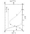
- Figure 3 is a graph showing the ratio of the length L and width W of the connecting member, a relationship between the current capacity I c-max of the joint surface current capacity I c and wire only.
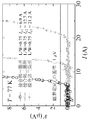
- FIG. 4 is a graph showing the measurement results of the electrical resistance when the number of junctions is one to three.
- FIG. 5 is a diagram for explaining the current flowing through the wire when the width W of the bonding portion is smaller than the wire width Ww.
- FIG. 6 is a view showing an outline of a connector in the third embodiment.
- FIG. 1 (A) is a side view of the connection of the high temperature superconducting wire
- FIG. 1 (B) is a top view of the connection of the high temperature superconducting wire
- FIG. 1C is a schematic view showing the flow of current in the high temperature superconducting wire.
- connection body of the high temperature superconducting wire material in the present embodiment is formed by connecting two high temperature superconducting wire materials 11 and 12 via a plurality of high temperature superconducting bulk bodies 13a, 13b, 13c and 13d.
- the high temperature superconducting wire may be referred to as a wire
- the high temperature superconducting bulk may be referred to as a bulk to simplify the description.
- bulk body 13a, 13b, 13c, 13d may be generically named the bulk body 13.
- the wires 11 and 12 are, for example, REBCO wires, and the bulk body 13 is a REBCO bulk having a melting point lower than that of the wires 11 and 12.
- the REBCO layer is exposed from the REBCO wire, a bulk 13 is placed between the wires, and heat treatment is performed to form a bond. Specific bonding methods are described in Non-Patent Document 1 and Patent Document 4.
- a plurality of junctions by the bulk body 13 are provided in parallel.
- the number may be any number as long as it is two or more.
- superconducting wires for NMR and MRI applications are required to have a junction current of about 100 amps (77 Kelvin & no magnetic field).
- about 10 amps (77 Kelvin & no magnetic field) is considered to be the limit that can flow in a single junction.
- the current capacity can be increased to 100 amperes by setting the number of junctions to ten.
- the wires 11 and 12 are connected via the bulk body 13 by the melt growth method has been described as an example, but the wires 11 and 12 may be directly connected by the melt diffusion method or the solid phase diffusion method. .
- the same principle as described above it is possible to significantly increase the current capacity which can be flowed throughout the connection.
- the two high temperature superconducting wires 11 and 12 are connected via the bulk body 13.
- the high temperature superconducting wires 11 and 12 are REBCO wires
- the bulk body 13 is a REBCO bulk body having a melting point lower than that of the wires 11 and 12.
- the wires 11 and 12 are generally composite wires including a stabilization layer, a substrate and the like in addition to the REBCO layer (high temperature superconducting layer).
- the REBCO layer is formed of a rare earth based superconducting material (REBa 2 Cu 3 O 7- ⁇ ) in the form of a tape (layered).
- the rare earth elements include Sc, Y, La, Ce, Pr, Nd, Pm, Sm, Eu, Gd, Tb, Dy, Ho, Er, Tm, Yb, and Lu.
- the wire 11 and the rare earth based superconducting material of the wire 12 may be the same or different.
- the melting point of the REBCO layer is required to be higher than the melting point of the bulk body 13.
- a REBCO wire having a REBCO layer using Gd, Y, or Gd and Y is in circulation.
- Gd is a preferable material because it has a relatively high melting point of about 1050 to 1100.degree.
- the REBCO layer of the wire 11 and the REBCO layer of the wire 12 may be made of different rare earth superconducting materials.
- REBCO wire has a multilayer structure made of a plurality of materials for mechanical reinforcement and electrical protection.
- An example of the structure of the REBCO wire is shown in FIG. As shown in the figure, from the lower layer side, copper stabilization layer 201 (15 ⁇ m), silver stabilization layer 202 (5 ⁇ m), substrate 203 (150 ⁇ m), intermediate layer (not shown, ⁇ 0.2 ⁇ m), REBCO layer 204 ( 3 ⁇ m), a silver stabilization layer 205 (10 ⁇ m), and a copper stabilization layer 206 (15 ⁇ m).
- the REBCO layer of REBCO wire corresponds to the high temperature superconducting layer in the present invention.
- the REBCO layer 204 In order to bond the wires 11 and 12 to the bulk body 13, the REBCO layer 204 needs to be in contact with the bulk body 13. Therefore, a pretreatment that exposes the REBCO layer 204 by stripping off the copper and silver stabilization layers (and possibly the substrate) is required. Moreover, in order to perform high temperature baking in a joining process, it is necessary to remove the material which has melting
- the bulk body 13 is made of a rare earth based superconducting material (RE'Ba 2 Cu 3 O 7 - ⁇ ) like the superconducting layers of the wires 11 and 12, but it is not a wire but a bulk.
- RE ′ is one or more rare earth elements (Sc, Y, La, Ce, Pr, Nd, Pm, Sm, Eu, Gd, and the like) of an element or composition different from RE in the REBCO layer of the REBCO wire 10 Tb, Dy, Ho, Er, Tm, Yb, Lu).
- the melting point of the bulk body 13 needs to be lower than the melting point of the REBCO layer of the wires 11 and 12 at least in the firing process.
- the firing temperature can be lowered as the melting point of the bulk body 13 is lower, it is desirable that the melting point of the bulk body 13 be low. Therefore, it is preferable that the rare earth elements in the bulk body 13 contain Y, Yb, Er, Ho or the like having a low melting point as a main component.
- the surfaces of the bulk body 13 are crystallized by crystal growth. It is not necessary to crystal-grow the entire bulk body to a perfect single crystal, and as long as it is single crystal only for the contact surface, the other part may be polycrystalline.
- the thickness of the single crystal layer may be an amount sufficient to obtain sufficient bonding strength. For example, sufficient bonding strength can be obtained with a thickness of several hundred nm (100 to 500 nm) or more, and the baking time for obtaining crystal growth of about 1 ⁇ m in YbBCO may be about one hour.
- the critical current of the bulk body 13 is related to the type of the contained rare earth element, the purity, and the shape.
- the rare earth element contained in the bulk body 13 may be of any type.
- the purity of the bulk body 13 is 10% or more, preferably 50% or more, and more preferably 70% or more.
- commercially available single crystal bulk bodies have non-superconducting substances (normal conductors or insulators) in order to maintain their shape during heating and manufacturing. Many may be introduced. Since the electrical conductivity changes depending on the purity of the bulk body, the purity of the bulk body may be 10% or more, but preferably 50% or more as much as possible.
- the critical current and the mechanical strength can be increased by adjusting the thickness of the bulk body 13 (height H in FIG. 1A). It is desirable that the thickness of the superconducting layer of the wire be greater than 3 ⁇ m in order for the molten bulk to spread to the superconducting layer of the wire at the time of high temperature bonding to obtain a sufficient bonding interface. Therefore, the bulk 13 needs to have a thickness of 1 ⁇ m or more. However, considering the preparation of bulk alone and the setting before bonding process, bulk of 20 ⁇ m or more is convenient to handle. The upper limit of the thickness is determined by the bulk production method and the ease of use of the connector, but may be 10 mm or less. Therefore, the height H may be appropriately selected in the range of 0.001 mm to 10 mm. The heights H of the plurality of bulk bodies 13 may be the same or different, but the height H is preferably the same for all the bulk bodies 13 in consideration of the ease of manufacture.
- the shape of the bulk body 13 is preferably symmetrical, and a rectangle, a rounded rectangle, or an ellipse can be adopted.
- L the length of the wire longitudinal direction of the bulk body 13
- W the length of the width direction
- the spacing G between adjacent bulk bodies 13 may be a spacing that does not combine during heat treatment, and may be, for example, 1 to 100 mm.
- the distance G may be 10 mm.
- the REBCO bulk body 13 is prepared.
- the bulk body 13 may be produced by itself, or may be a commercially available product.
- the preparation method there are a sintering method, an organic acid salt method and the like, and in the latter, high purity can be manufactured.
- REBCO wires 11 and 12 are prepared. Since the REBCO wire 10 has a multilayer structure, it is necessary to remove the protective layer so that the REBCO layer is exposed. There are two methods for exposing the REBCO layer: a method in which the REBCO layer 204 is exposed to the substrate 203 side and a method in which the substrate 203 side is removed. In any case, when the end of the REBCO wire is put into liquid nitrogen and quenched to cryogenic temperature (77 K) and then taken out and applied force, the thermal stress of incomplete restraint among the materials allows the respective materials to be properly separated. . Note that depending on the stress direction, any surface of the REBCO layer 204 can be exposed.
- a plurality of bulk bodies 13 may be simultaneously heated and jointed simultaneously, or heat treatment may be performed independently. However, when heating a plurality of bulk bodies 13 simultaneously with one temperature controller, temperature variations may occur in the respective bulk bodies 13. Therefore, bonding may be simultaneously performed while temperature control is performed using a plurality of temperature controllers, It is desirable to heat separately alone.
- REBCO wires under development by Sumitomo Electric Industries, Ltd. were prepared as REBCO wires 11 and 12.
- the REBCO layer of this wire mainly contains Gd as a rare earth element and also contains Y, and its melting point is about 1000-1100 ° C. (in air).
- the bulk body 13 the bulk body of Yb123 which mainly contains Yb as a rare earth element was utilized as the bulk body of Yb123 which mainly contains Yb as a rare earth element was utilized.
- the melting point of Yb123 bulk is about 930 ° C. (in air).
- the critical current I c of the entire junction is shown by black circles and dotted lines, and the critical current I c -max of the wire only is shown by white circles and solid lines.
- the critical current is measured by measuring the voltage while increasing the amount of current in liquid nitrogen (77 K).
- the critical current I c becomes larger as L is increased when W is fixed.
- the critical current I c-max of the wire is reduced due to the deterioration accompanying the heat treatment than the critical current before the heat treatment.
- the reason for the decrease is considered to be the performance deterioration due to the diffusion of the metal material (Ni, Fe, etc.) of the wire substrate into the superconducting layer and the cracking of the superconducting ceramic layer (REBCO layer) due to high temperature firing.
- the critical current of the entire connection can be increased by increasing the number of junctions.
- the bulk body length L is determined in consideration of the decrease in the critical current I c-max of the wire itself accompanying the deterioration of the heat treatment. It is necessary to If L / W ⁇ 1.5, more preferably L / W ⁇ 1, and more preferably L / W ⁇ 0.75, a sufficiently large critical current can be obtained. Also, if L / W is reduced, the number of junctions must be increased to obtain the same critical current, and the entire connection becomes long. Therefore, L / W is preferably greater than 0.1, and more preferably greater than 0.25.
- the melt growth method can perform bonding in a short time as compared with other methods. Therefore, according to the present embodiment, a connector having a large current capacity can be manufactured in a short time.
- the amount of current that can be applied to the junction is proportional to the junction area. Therefore, the amount of current per one junction changes depending on the magnitude of W even if L / W is constant.
- I c -pass I c-ow ⁇ (Ww-W) / Ww.
- I c -pass I c-ow ⁇ (Ww-W) / Ww.
- Ww 4 mm
- W 2 mm
- L 1.5 mm
- I c ⁇ ow 200 A
- I c ⁇ max 100 A
- the current capacity per junction can be determined. Therefore, by simple calculation, the junction for obtaining the required current capacity as a whole of the connector. The number is determined.
- the width W of the bulk body smaller than the wire width Ww, a connection body with a larger current capacity than that of the first embodiment can be obtained.
- the second embodiment can increase the current capacity as compared to the first embodiment, but has the disadvantage that the number of junctions increases and the overall length of the connection increases. So, in this embodiment, the number of junctions is reduced without reducing current capacity, and the connection method which can shorten the length of a connection part is adopted.
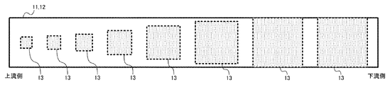
- the width W of the bulk body is gradually increased from the upstream side to the downstream side.
- “slightly larger” means a broad monotonous increase, and the widths of adjacent bulk bodies may be the same.
- two wires are connected so that the current flows back.
- the end remote from the current source is referred to as the distal end
- the side near the distal end is downstream and the side remote from the distal end is upstream.
- the bulk body 13a is located on the most upstream side
- the bulk body 13d is located on the most downstream side. Therefore, the width W of the bulk body 13a is the smallest, and the width W of the bulk body 13d is the largest.
- the amount of current flowing through the wire decreases toward the downstream side. Therefore, since the critical current of only the wire can be made smaller on the downstream side than on the upstream side, the bonding surface area can be increased and the current capacity at the bonding surface can be increased. By increasing the junction surface current capacity, the required number of junctions can be reduced.
- FIG. 6 shows an example of a joined body according to the present embodiment.
- the number of joints is eight.
- W (and L) may be gradually increased toward the downstream side.
- L may be gradually increased toward the downstream side while keeping W constant.
- W may be gradually increased toward the downstream side while keeping L constant.
- W and L may be gradually increased toward the downstream side, and L / W may be in a predetermined range (the value of L / W may be increased or decreased). That is, at least one of W and L for a plurality of junctions may be determined so as to monotonously increase from the upstream side toward the downstream side.
- the critical current in the entire junction can be increased, and furthermore, the length of the entire junction can be shortened.
- the two wires may be brought into contact with each other for direct connection without using the bulk body.
- a melt diffusion method and a solid phase diffusion method can be mentioned.
- the present invention can increase the critical current in the connection of high temperature superconducting wire.
- the present invention can be used to fabricate a sufficiently long high temperature superconducting wire for use in the development of any superconducting magnet (superconducting coil), in particular in permanent current mode as in MRI and NMR devices It can be applied to application devices that require the operation of
Abstract
Provided is a high-temperature superconductor wire connection in which high-temperature superconductor wires comprising high-temperature superconductor layers are connected to each other; wherein facing first and second high-temperature superconductor wires are connected at multiple discrete joining locations along the lengthwise direction of the first and second high-temperature superconductor wires. Each of the multiple joining locations is one of rectangular, rounded rectangular, or elliptical in shape, and, defining L as the length of the high-temperature superconductor wires in the longitudinal direction as L and the length thereof in the widthwise direction as W, it is preferable that L/W be 0.5, more preferably 0.25 < L/W < 0.75. Width W and/or length L preferably monotonically increases or decreases from upstream to downstream along the lengthwise direction of the wires.
Description
本発明は、高温超伝導線材の接続体に関する。
The present invention relates to a connection of high temperature superconducting wires.
超伝導線材は、NMR(Nuclear Magnetic Resonance)装置や、MRI(Magnetic Resonance Imaging)装置などに広く用いられている。近年は、希土類系の高温超伝導線材(REBCO超伝導線材)が生産されており、これを用いた研究開発が行われている。
Superconducting wires are widely used in NMR (Nuclear Magnetic Resonance) devices, MRI (Magnetic Resonance Imaging) devices, and the like. In recent years, high-temperature superconducting wires (REBCO superconducting wires) of a rare earth system have been produced, and research and development using this have been conducted.
超伝導線材同士の接続は、線材の長尺化や永久電流モードの実現などのために、必要不可欠な技術的課題である。REBCO超伝導線材同士の低抵抗接続は、従来は半田付けによって行われており、この手法では約10-8Ωの電気抵抗値が発生してしまうことが知られている。
The connection between the superconducting wires is an indispensable technical issue for lengthening of the wires and realization of a permanent current mode. The low resistance connection between REBCO superconducting wires is conventionally performed by soldering, and it is known that this method generates an electrical resistance value of about 10 −8 Ω.
近年、REBCO超伝導線材同士を直接接続する研究が行われており、特許文献1では溶融拡散法という手法が提案されている。この手法では、2つのREBCO超伝導線材の保護層を除去し、超伝導層同士を当接して加圧しながら、超伝導層の溶融点まで加熱することによって当接させた超伝導層の厚さ方向の一部を溶融拡散して超伝導線材同士を接合する。これにより、REBCO超伝導線材同士を、半田付けによる接続よりも低抵抗に接続することができると報告されている。同様の手法は、特許文献2-3においても提案されている。
In recent years, research has been conducted to directly connect REBCO superconducting wires, and Patent Document 1 proposes a method called a melt diffusion method. In this method, the protective layer of the two REBCO superconducting wires is removed, and the thickness of the superconducting layer brought into contact by heating to the melting point of the superconducting layer while pressing the superconducting layers into contact with each other. The superconducting wires are joined together by melting and diffusing a part of the direction. It is reported that this enables the REBCO superconducting wires to be connected with lower resistance than the connection by soldering. A similar approach is also proposed in Patent Documents 2-3.
また、本発明者らは、特許文献4・非特許文献1において、高温超伝導バルク体を介した間接的な高温超伝導線材の接続手法(溶融成長法)を提案している。この手法は、高温超伝導バルク体を溶融し、高温超伝導層を種結晶として結晶成長させることにより、高温超伝導層と高温超伝導バルク体とを接続する手法である。この手法は、溶融拡散法と比較して短時間で接続が行え、また、接続の機械的強度が強いという利点がある。
Moreover, the present inventors have proposed the connection method (melt growth method) of the high temperature superconducting wire connection indirectly via a high temperature superconducting bulk body in Patent Document 4 and Non-Patent Document 1. This method is a method of connecting the high temperature superconducting layer and the high temperature superconductor bulk by melting the high temperature superconductor bulk and crystal-growing the high temperature superconductor layer as a seed crystal. This method has an advantage that connection can be performed in a short time as compared with the melt diffusion method, and the mechanical strength of the connection is strong.
上述したいずれの接続方法においても、最大の技術的課題は、超伝導接続の電流容量を高めることである。バルクを用いた接合方法はこれまで電流容量がそれほど多くなかった。また、溶融拡散法では、電流容量を増やすためには1週間以上の長い熱処理が必要となる。
In any of the connection methods described above, the biggest technical issue is to increase the current capacity of the superconducting connection. So far, the bulk bonding method has not so much current capacity. In addition, in the melt diffusion method, a long heat treatment of one week or more is required to increase the current capacity.
このような課題を考慮し、本発明は、高温超伝導線材の接続において、大きな電流容量の接続を製造可能な技術を提供することを目的とする。
In view of such problems, the present invention aims to provide a technology capable of manufacturing a connection of a large current capacity in the connection of a high temperature superconducting wire.
上記課題を解決するために、本発明においては、高温超伝導線材同士を接続する際に、互いに分離した複数の接合箇所においてこれらの線材を接続する。より具体的には、本発明は、高温超伝導層を含む高温超伝導線材同士が接続された高温超伝導線材の接続体であって、対向する第1の高温超伝導線材と第2の高温超伝導線材とが、当該第1の高温超伝導線材および第2の高温超伝導線材の長手方向に沿って互いに分離している複数の接合箇所において接続されている、ことを特徴とする。
In order to solve the above-mentioned subject, in the present invention, when connecting high temperature superconductivity wire rods, these wires are connected in a plurality of joined parts which separated mutually. More specifically, the present invention is a connecting body of high temperature superconducting wires in which high temperature superconducting wires including a high temperature superconducting layer are connected to each other, and the first high temperature superconducting wire and the second high temperature facing each other It is characterized in that the superconducting wire is connected at a plurality of junctions separated from each other along the longitudinal direction of the first high temperature superconducting wire and the second high temperature superconducting wire.
本発明において、前記複数の接合箇所のそれぞれは、矩形、角丸矩形、楕円形のいずれかであってよく、前記高温超伝導線材長手方向の長さをL、幅方向の長さをWとしたときに、0.1<L/W<1.5を満たすことが好ましい。また、0.25<L/W<0.75を満たすことがより望ましい。
In the present invention, each of the plurality of bonding points may be any of a rectangle, a rounded rectangle, and an ellipse, and the length in the longitudinal direction of the high-temperature superconducting wire is L and the length in the width direction is W It is preferable that the condition of 0.1 <L / W <1.5 is satisfied. In addition, it is more desirable to satisfy 0.25 <L / W <0.75.
本発明において、前記複数の接合箇所についての前記Wおよび/または前記Lは、前記高温超伝導線材長手方向に沿って、上流側から下流側に向かって単調増加することが好ましい。
In the present invention, it is preferable that W and / or L for the plurality of bonding points monotonously increase from the upstream side to the downstream side along the longitudinal direction of the high-temperature superconducting wire.
本発明によれば、大きな電流容量を持つ高温超伝導線材の接続を提供可能である。
According to the present invention, it is possible to provide a connection of a high temperature superconducting wire having a large current capacity.
以下では、図面を参照しながら、この発明を実施するための形態を説明する。
Hereinafter, embodiments of the present invention will be described with reference to the drawings.
[第1の実施形態]
<概要>
図1(A)は高温超伝導線材の接続体の側面図であり、図1(B)は高温超伝導線材の接続体の上面図である。図1(C)は高温超伝導線材における電流の流れを示す模式図である。 First Embodiment
<Overview>
FIG. 1 (A) is a side view of the connection of the high temperature superconducting wire, and FIG. 1 (B) is a top view of the connection of the high temperature superconducting wire. FIG. 1C is a schematic view showing the flow of current in the high temperature superconducting wire.
本実施形態における高温超伝導線材の接続体は、2本の高温超伝導線材11,12を、複数の高温超伝導バルク体13a,13b,13c,13dを介して接続したものである。なお、以下では記載の簡略化のために、高温超伝導線材のことを線材、高温超伝導バルク体をバルク体と称する場合がある。また、バルク体13a,13b,13c,13dを総称して、バルク体13と称する場合もある。
The connection body of the high temperature superconducting wire material in the present embodiment is formed by connecting two high temperature superconducting wire materials 11 and 12 via a plurality of high temperature superconducting bulk bodies 13a, 13b, 13c and 13d. In the following, the high temperature superconducting wire may be referred to as a wire, and the high temperature superconducting bulk may be referred to as a bulk to simplify the description. Moreover, bulk body 13a, 13b, 13c, 13d may be generically named the bulk body 13.
線材11,12は例えばREBCO線材であり、バルク体13は線材11,12よりも低い融点を有するREBCOバルク体である。
The wires 11 and 12 are, for example, REBCO wires, and the bulk body 13 is a REBCO bulk having a melting point lower than that of the wires 11 and 12.
溶融成長法では、REBCO線材からREBCO層を露出させ、線材間にバルク13を設置して熱処理することにより接合を形成する。具体的な接合方法は非特許文献1や特許文献4に記載されている。
In the melt growth method, the REBCO layer is exposed from the REBCO wire, a bulk 13 is placed between the wires, and heat treatment is performed to form a bond. Specific bonding methods are described in Non-Patent Document 1 and Patent Document 4.
図に示されるように、バルク体13による接合が並列に複数設けられる。図1(A)(B)では、接合は4カ所であるが、その数は2以上であれば何個であってもよい。個々の接合箇所において流せる最大電流には上限があるが、接合を並列に設置することにより、接続体全体に流れる電流を増加させることができる。例えば、NMRやMRI用途の超伝導線では接合電流として100アンペア程度(77ケルビン&無磁場)のものが要求される。バルクを介した接合では10アンペア程度(77ケルビン&無磁場)が単一の接合で流せる限界と考えられる。本手法では、接合の数を10個とすることで、電流容量を100アンペアまで増加させることができる。
As shown in the figure, a plurality of junctions by the bulk body 13 are provided in parallel. In FIGS. 1 (A) and 1 (B), there are four junctions, but the number may be any number as long as it is two or more. There is an upper limit to the maximum current that can flow at each junction, but placing the junctions in parallel can increase the current flowing across the connection. For example, superconducting wires for NMR and MRI applications are required to have a junction current of about 100 amps (77 Kelvin & no magnetic field). In bulk junctions, about 10 amps (77 Kelvin & no magnetic field) is considered to be the limit that can flow in a single junction. In this method, the current capacity can be increased to 100 amperes by setting the number of junctions to ten.
ここでは、溶融成長法によってバルク体13を介して線材11,12を接続する場合を例にとって説明したが、溶融拡散法や固相拡散法などによって線材11,12同士を直接接続してもよい。上記と同様の原理により、接続体全体に流せる電流容量を大幅に増加させることができる。
Here, the case where the wires 11 and 12 are connected via the bulk body 13 by the melt growth method has been described as an example, but the wires 11 and 12 may be directly connected by the melt diffusion method or the solid phase diffusion method. . By the same principle as described above, it is possible to significantly increase the current capacity which can be flowed throughout the connection.
なお、一般に接続部が磁場にさらされると、電流容量が無磁場の場合の数分の一に減少する。温度77ケルビンから4.2ケルビンになると8倍程度増加する。その意味で、機器の運転温度4.2ケルビン&磁場下で200アンペアの電流容量を得ようとすれば、この減少分を見込んで、温度77ケルビン&無磁場で100アンペア程度を流せる必要がある。単一の接合によって短時間でこのように大きな電流容量を得ることはほぼ不可能であるが、本手法によれば複数の接合を並列に形成することにより、この程度の大きな電流容量を得ることができる。
Generally, when the connection is exposed to a magnetic field, the current capacity is reduced to a fraction of that in the absence of a magnetic field. The temperature increases from 77 Kelvin to 4.2 Kelvin by about eight times. In that sense, if it is intended to obtain a current capacity of 200 amps under the operating temperature of 4.2 Kelvin & magnetic field of the equipment, it is necessary to allow about 100 amps to flow at 77 Kelvin & no magnetic field in anticipation of this decrease . It is almost impossible to obtain such a large current capacity in a short time by a single junction, but according to the present method, such a large current capacity can be obtained by forming a plurality of junctions in parallel. Can.
<接続方法>
上述のように、2本の高温超伝導線材11,12を、バルク体13を介して接続する。ここで、高温超伝導線材11,12はREBCO線材であり、バルク体13は線材11,12よりも低い融点を有するREBCOバルク体である。 <Connection method>
As described above, the two high temperature superconducting wires 11 and 12 are connected via the bulk body 13. Here, the high temperature superconducting wires 11 and 12 are REBCO wires, and the bulk body 13 is a REBCO bulk body having a melting point lower than that of the wires 11 and 12.
上述のように、2本の高温超伝導線材11,12を、バルク体13を介して接続する。ここで、高温超伝導線材11,12はREBCO線材であり、バルク体13は線材11,12よりも低い融点を有するREBCOバルク体である。 <Connection method>
As described above, the two high temperature
線材11,12は、一般には、REBCO層(高温超伝導層)の他に安定化層や基板などを含む複合線材である。REBCO層は、希土類系超伝導材料(REBa2Cu3O7-δ)をテープ状(層状)にしたものである。希土類元素には、Sc,Y,La,Ce,Pr,Nd,Pm,Sm,Eu,Gd,Tb,Dy,Ho,Er,Tm,Yb,Luが含まれる。線材11と線材12の希土類系超伝導材料は同一であってもよいし異なっていてもよい。溶融成長法では、バルク体13を結晶成長させるので、REBCO層の融点は、バルク体13の融点よりも高いことが必要とされる。REBCO線材として、Gd、Y、あるいはGdとYを用いたREBCO層を有するものが一般に流通している。特にGdは1050~1100℃程度の比較的高い融点を持つので好ましい材料である。なお、線材11のREBCO層と線材12のREBCO層は、異なる希土類超伝導材料からなってもよい。
The wires 11 and 12 are generally composite wires including a stabilization layer, a substrate and the like in addition to the REBCO layer (high temperature superconducting layer). The REBCO layer is formed of a rare earth based superconducting material (REBa 2 Cu 3 O 7-δ ) in the form of a tape (layered). The rare earth elements include Sc, Y, La, Ce, Pr, Nd, Pm, Sm, Eu, Gd, Tb, Dy, Ho, Er, Tm, Yb, and Lu. The wire 11 and the rare earth based superconducting material of the wire 12 may be the same or different. In the melt growth method, since the bulk body 13 is crystal-grown, the melting point of the REBCO layer is required to be higher than the melting point of the bulk body 13. Generally, a REBCO wire having a REBCO layer using Gd, Y, or Gd and Y is in circulation. In particular, Gd is a preferable material because it has a relatively high melting point of about 1050 to 1100.degree. The REBCO layer of the wire 11 and the REBCO layer of the wire 12 may be made of different rare earth superconducting materials.
一般に市販されているREBCO線材は、機械的な補強や電気的な保護のために、複数の材料からなる多層構造を有する。図2にREBCO線材の構造の一例を示す。図に示すように、下層側から、銅安定化層201(15μm)、銀安定化層202(5μm)、基板203(150μm)、中間層(不図示、~0.2μm)、REBCO層204(3μm)、銀安定化層205(10μm)、銅安定化層206(15μm)を有する。REBCO線材のREBCO層が、本発明における高温超伝導層に相当する。
Generally, commercially available REBCO wire has a multilayer structure made of a plurality of materials for mechanical reinforcement and electrical protection. An example of the structure of the REBCO wire is shown in FIG. As shown in the figure, from the lower layer side, copper stabilization layer 201 (15 μm), silver stabilization layer 202 (5 μm), substrate 203 (150 μm), intermediate layer (not shown, ̃0.2 μm), REBCO layer 204 ( 3 μm), a silver stabilization layer 205 (10 μm), and a copper stabilization layer 206 (15 μm). The REBCO layer of REBCO wire corresponds to the high temperature superconducting layer in the present invention.
線材11,12をバルク体13と接合するためには、REBCO層204をバルク体13に接触させる必要がある。したがって、銅安定化層や銀安定化層(場合によって基板も)剥離して、REBCO層204を露出させる前処理が必要となる。また、接合過程において高温焼成を行うため、焼成温度以下の融点を有する材料は取り除く必要がある。焼成温度はバルク体13の融点に応じて決まるが、700℃あるいはそれ以上となる。したがって、線材に半田が用いられている場合には取り除く必要がある。また、焼成温度が900℃を超える場合には、銀や銀合金(融点が900℃前後)を取り除くことが望ましい。これらの材料を除去する方法については、後ほど詳しく説明する。
In order to bond the wires 11 and 12 to the bulk body 13, the REBCO layer 204 needs to be in contact with the bulk body 13. Therefore, a pretreatment that exposes the REBCO layer 204 by stripping off the copper and silver stabilization layers (and possibly the substrate) is required. Moreover, in order to perform high temperature baking in a joining process, it is necessary to remove the material which has melting | fusing point below a calcination temperature. The firing temperature is determined depending on the melting point of the bulk body 13 but is 700 ° C. or more. Therefore, if solder is used for the wire, it needs to be removed. When the firing temperature exceeds 900 ° C., it is desirable to remove silver or a silver alloy (having a melting point of about 900 ° C.). The method of removing these materials will be described in detail later.
バルク体13は、線材11,12の超伝導層と同様に希土類系超伝導材料(RE’Ba2Cu3O7-δ)からなるが、線材ではなくバルク体である。ここで、RE’は、REBCO線材10のREBCO層におけるREとは異なる元素または組成の一つまたは複数の希土類元素(Sc,Y,La,Ce,Pr,Nd,Pm,Sm,Eu,Gd,Tb,Dy,Ho,Er,Tm,Yb,Lu)を表す。バルク体13の融点は、少なくとも焼成過程においては、線材11,12のREBCO層の融点よりも低い必要がある。また、バルク体13の融点が低いほど焼成温度を低くすることができるので、バルク体13の融点は低いことが望ましい。そのため、バルク体13中の希土類元素は、融点が低いY,Yb,Er,Hoなどを主成分とすることが好ましい。
The bulk body 13 is made of a rare earth based superconducting material (RE'Ba 2 Cu 3 O 7 -δ ) like the superconducting layers of the wires 11 and 12, but it is not a wire but a bulk. Here, RE ′ is one or more rare earth elements (Sc, Y, La, Ce, Pr, Nd, Pm, Sm, Eu, Gd, and the like) of an element or composition different from RE in the REBCO layer of the REBCO wire 10 Tb, Dy, Ho, Er, Tm, Yb, Lu). The melting point of the bulk body 13 needs to be lower than the melting point of the REBCO layer of the wires 11 and 12 at least in the firing process. In addition, since the firing temperature can be lowered as the melting point of the bulk body 13 is lower, it is desirable that the melting point of the bulk body 13 be low. Therefore, it is preferable that the rare earth elements in the bulk body 13 contain Y, Yb, Er, Ho or the like having a low melting point as a main component.
また、REBCOの化学式REBa2Cu3O7-δにおいて酸素量が小さいほど融点は低くなるので、より低い温度で接続体を作製するためには、元の結晶構造を維持できる範囲内でできるだけ酸素量が少ないバルク体を用意することが好ましい。具体的には、焼成過程前のバルク体20の酸素量はδが-1~4の範囲内であることが好ましく、0.5~2の範囲内であることがより好ましい。
In addition, the lower the amount of oxygen in REBCO's chemical formula REBa 2 Cu 3 O 7-δ , the lower the melting point. Therefore, in order to produce a connection at a lower temperature, oxygen is as low as possible within the range that can maintain the original crystal structure. It is preferable to prepare a small amount of bulk body. Specifically, it is preferable that δ be in the range of −1 to 4 and more preferably in the range of 0.5 to 2 before the baking process.
また、最終的に作製された接続体において、バルク体13と線材11、12および接合界面の臨界電流は酸素量に依存するので、接合後に、酸素補充用の熱処理を行って酸素量を増やし、超伝導性能を高めることが好ましい。
In addition, in the connection body finally manufactured, since the critical current of the bulk body 13 and the wires 11 and 12 and the bonding interface depends on the amount of oxygen, heat treatment for oxygen replenishment is performed to increase the amount of oxygen after bonding. It is preferred to enhance the superconducting performance.
バルク体13の表面のうち、少なくとも線材11,12のREBCO層と接触する表面は、結晶成長により結晶化されている。バルク体全体を完全な単結晶まで結晶成長させる必要はなく、接触表面についてのみ単結晶となっていれば、その他の部分は多結晶であってよい。単結晶層の厚さは、十分な接合強度が得られるだけの量であればよい。例えば、厚さ数百nm(100~500nm)以上で十分な接合強度が得られ、YbBCOにおいて1μm程度の結晶成長を得るための焼成時間は1時間程度で済む。
Among the surfaces of the bulk body 13, at least the surfaces of the wires 11 and 12 in contact with the REBCO layer are crystallized by crystal growth. It is not necessary to crystal-grow the entire bulk body to a perfect single crystal, and as long as it is single crystal only for the contact surface, the other part may be polycrystalline. The thickness of the single crystal layer may be an amount sufficient to obtain sufficient bonding strength. For example, sufficient bonding strength can be obtained with a thickness of several hundred nm (100 to 500 nm) or more, and the baking time for obtaining crystal growth of about 1 μm in YbBCO may be about one hour.
バルク体13の臨界電流は、含有されている希土類元素の種類と、純度と、形状に関係がある。バルク体13に含有される希土類元素は、任意の種類のものであって構わない。バルク体13の純度は、10%以上とし、50%以上とすることが好ましく、70%以上とすることが更に好ましい。純度70%以上の多結晶バルク体を作製することは難しくはないが、市販されている単結晶バルク体は加熱製造時の形状を保持するために非超伝導物質(常伝導または絶縁体)が多く導入される場合がある。バルク体の純度によって電気伝導性が変わるので、バルク体の純度は10%以上でよいが、できるだけ50%以上とすることが好ましい。
The critical current of the bulk body 13 is related to the type of the contained rare earth element, the purity, and the shape. The rare earth element contained in the bulk body 13 may be of any type. The purity of the bulk body 13 is 10% or more, preferably 50% or more, and more preferably 70% or more. Although it is not difficult to produce polycrystalline bulk bodies with a purity of 70% or more, commercially available single crystal bulk bodies have non-superconducting substances (normal conductors or insulators) in order to maintain their shape during heating and manufacturing. Many may be introduced. Since the electrical conductivity changes depending on the purity of the bulk body, the purity of the bulk body may be 10% or more, but preferably 50% or more as much as possible.
バルク体13の厚さ(図1(A)における高さH)を調整することで臨界電流と機械強度を大きくすることができる。高温接合時に溶融したバルクが線材の超伝導層に広がって十分な接合界面を得るには、線材の超伝導層の厚さ3μmより大きいことが望ましい。そのため、バルク13は厚さ1μm以上が必要である。しかし、バルク単体の作製と接合処理前のセッティングなど考慮すれば20μm以上のバルクが扱い便利である。厚さの上限はバルクの作製方法と接続体の使いやすさで決まるが、10mm以下でもよい。したがって、高さHは、0.001mm以上10mm以下の範囲で適宜選択すればよい。複数のバルク体13の高さHは同一であっても異なっていても構わないが、製造の容易さを考慮すると高さHは全てのバルク体13で同一であることが好ましい。
The critical current and the mechanical strength can be increased by adjusting the thickness of the bulk body 13 (height H in FIG. 1A). It is desirable that the thickness of the superconducting layer of the wire be greater than 3 μm in order for the molten bulk to spread to the superconducting layer of the wire at the time of high temperature bonding to obtain a sufficient bonding interface. Therefore, the bulk 13 needs to have a thickness of 1 μm or more. However, considering the preparation of bulk alone and the setting before bonding process, bulk of 20 μm or more is convenient to handle. The upper limit of the thickness is determined by the bulk production method and the ease of use of the connector, but may be 10 mm or less. Therefore, the height H may be appropriately selected in the range of 0.001 mm to 10 mm. The heights H of the plurality of bulk bodies 13 may be the same or different, but the height H is preferably the same for all the bulk bodies 13 in consideration of the ease of manufacture.
バルク体13の形状は、対称な形状であることが好ましく、矩形、角丸矩形、楕円形を採用することができる。以下では、図1(B)に示すように、バルク体13の線材長手方向の長さをL、幅方向の長さをWと称する。長さLや幅Wについては後述する。
The shape of the bulk body 13 is preferably symmetrical, and a rectangle, a rounded rectangle, or an ellipse can be adopted. Below, as shown to FIG. 1 (B), the length of the wire longitudinal direction of the bulk body 13 is called L, and the length of the width direction is called W. As shown in FIG. The length L and the width W will be described later.
隣接するバルク体13の間の間隔Gは、熱処理の際に合体してしまわない間隔であればよく、例えば、1~100mmとするとよい。なお、間隔Gは狭いほど接続部全体の長さを短くすることができ好適である。例えば、間隔Gは10mmとするとよい。
The spacing G between adjacent bulk bodies 13 may be a spacing that does not combine during heat treatment, and may be, for example, 1 to 100 mm. The smaller the distance G, the shorter the entire length of the connection portion, which is preferable. For example, the distance G may be 10 mm.
REBCO線材の接続処理の流れについて説明する。なお、溶融成長法は非特許文献1や特許文献4に記載されているので、ここでは簡単な説明にとどめる。
The flow of REBCO wire connection processing will be described. Note that the melt growth method is described in Non-Patent Document 1 and Patent Document 4, so only a brief explanation is given here.
まず、REBCOバルク体13を用意する。バルク体13は、自ら作製してもよいが、市販品を購入してきてもよい。作製方法において、焼結法と有機酸塩法などがあり、後者では高純度のものが製造可能である。また、必要に応じて、バルク体13の融点を下げるために酸素欠損を導入する熱処理(急冷)を施すことが好ましい。
First, the REBCO bulk body 13 is prepared. The bulk body 13 may be produced by itself, or may be a commercially available product. In the preparation method, there are a sintering method, an organic acid salt method and the like, and in the latter, high purity can be manufactured. In addition, it is preferable to perform heat treatment (quenching) for introducing oxygen vacancies in order to lower the melting point of the bulk body 13 as necessary.
また、REBCO線材11,12を用意する。REBCO線材10は多層構造を有しているので、REBCO層が露出するように保護層を除去する必要がある。REBCO層を露出する方法として、REBCO層204が基板203側に付いた状態で露出させる方法と、基板203側を除去する方法の2つの方法がある。いずれにおいても、REBCO線材の端部を液体窒素中に入れて極低温(77K)まで急冷した後に取り出して力を加えると、材料間における不完全拘束の熱応力によって、各材料を適切に分離できる。なお、応力方向によって、REBCO層204のいずれの面を露出させることもできる。
In addition, REBCO wires 11 and 12 are prepared. Since the REBCO wire 10 has a multilayer structure, it is necessary to remove the protective layer so that the REBCO layer is exposed. There are two methods for exposing the REBCO layer: a method in which the REBCO layer 204 is exposed to the substrate 203 side and a method in which the substrate 203 side is removed. In any case, when the end of the REBCO wire is put into liquid nitrogen and quenched to cryogenic temperature (77 K) and then taken out and applied force, the thermal stress of incomplete restraint among the materials allows the respective materials to be properly separated. . Note that depending on the stress direction, any surface of the REBCO layer 204 can be exposed.
そして、露出させた2つの線材11,12のREBCO面がバルク体13を挟むように、線材11,12とバルク体13をセットして加熱炉に入れ、バルク体13の融点以上かつ線材11,12の融点未満の温度まで加熱する。これにより、バルク体13が液相状態になる。その後、徐冷することで線材11,12と接触するバルク体13の表面は、線材11,12のREBCOを種結晶として結晶成長する。最後に、超伝導性能を回復させるために、REBCO材料内に酸素を付加するための熱処理を施す。
Then, set the wire rods 11 and 12 and the bulk body 13 so that the REBCO surfaces of the exposed two wire rods 11 and 12 sandwich the bulk body 13 and put them in a heating furnace. Heat to a temperature below the 12 melting point. Thereby, the bulk body 13 will be in a liquid phase state. Thereafter, by slow cooling, the surface of the bulk body 13 in contact with the wires 11 and 12 undergoes crystal growth using REBCO of the wires 11 and 12 as a seed crystal. Finally, a heat treatment is applied to add oxygen into the REBCO material to restore the superconducting performance.
なお、複数のバルク体13を同時に加熱して同時に接合を行ってもよいし、それぞれ単独で熱処理を行ってもよい。ただし、一つの温度コントローラーで複数のバルク体13を同時に加熱するとそれぞれのバルク体13において温度にばらつきが生じることがあるので、複数の温度コントローラーを用いてそれぞれ温度制御しながら同時に接合をするか、単独で別々に加熱することが望ましい。
A plurality of bulk bodies 13 may be simultaneously heated and jointed simultaneously, or heat treatment may be performed independently. However, when heating a plurality of bulk bodies 13 simultaneously with one temperature controller, temperature variations may occur in the respective bulk bodies 13. Therefore, bonding may be simultaneously performed while temperature control is performed using a plurality of temperature controllers, It is desirable to heat separately alone.
<実験1:単一接合>
まず、接合部(バルク体13)を1つとして、臨界電流を測定した。 Experiment 1: Single Bonding
First, the critical current was measured with one junction (bulk body 13).
まず、接合部(バルク体13)を1つとして、臨界電流を測定した。 Experiment 1: Single Bonding
First, the critical current was measured with one junction (bulk body 13).
この実験では、REBCO線材11,12として、住友電気工業株式会社が開発中のREBCO線を用意した。この線材は、図2に示す構造を有し、幅4mm(Ww=4mm)、厚さ約0.2mmである。この線材のREBCO層は、希土類元素として、Gdを主として含み、Yも含まれており、その融点は約1000-1100℃(大気中)である。また、バルク体13として、希土類元素としてYbを主に含むYb123のバルク体を利用した。Yb123バルクの融点は約930℃(大気中)である。
In this experiment, REBCO wires under development by Sumitomo Electric Industries, Ltd. were prepared as REBCO wires 11 and 12. This wire has the structure shown in FIG. 2 and is 4 mm wide (Ww = 4 mm) and about 0.2 mm thick. The REBCO layer of this wire mainly contains Gd as a rare earth element and also contains Y, and its melting point is about 1000-1100 ° C. (in air). Moreover, as the bulk body 13, the bulk body of Yb123 which mainly contains Yb as a rare earth element was utilized. The melting point of Yb123 bulk is about 930 ° C. (in air).
バルク体13の幅Wを線材幅Wwと同じ4mmに固定し、バルク体13の長さLを変えた実験を行い、接続全体の臨界電流Icと線材のみの臨界電流Ic-maxを計測した。線材のみの臨界電流Ic-maxは、接合に伴う線材の劣化を反映する。バルク体幅Wが線材幅Wwと等しい場合には、臨界電流Ic-maxは、接合箇所を増やすことにより増加可能な接続全体の臨界電流の上限となる。
An experiment was performed in which the width W of the bulk body 13 was fixed to 4 mm equal to the wire width Ww and the length L of the bulk body 13 was changed, and the critical current I c of the entire connection and the critical current I c-max of only the wire were measured did. The critical current I c -max of the wire alone reflects the deterioration of the wire due to the bonding. When the bulk body width W is equal to the wire width Ww, the critical current I c -max is the upper limit of the critical current of the entire connection that can be increased by increasing the number of joints.
バルク体長さL = 0.5mm, 1mm, 2mm, 3mm, 4mm, 5mm, 12mm, 16mm, 20mmの場合について実験を行った。いずれにおいても、バルク体の高さHは0.05mmで固定とした。加熱は、到達温度930℃で1分保持の条件で行った。実験結果を図3のグラフに示す。
The experiments were conducted for the cases of bulk length L = 0.5 mm, 1 mm, 2 mm, 3 mm, 4 mm, 5 mm, 12 mm, 16 mm and 20 mm. In any case, the height H of the bulk was fixed at 0.05 mm. The heating was performed under the condition of holding at a final temperature of 930 ° C. for 1 minute. The experimental results are shown in the graph of FIG.
接合全体の臨界電流Icは黒丸および点線で示され、線材のみの臨界電流Ic-maxは白丸および実線で示されている。液体窒素中(77K)で電流量を増やしながら電圧の測定を行うことで、臨界電流を測定している。
The critical current I c of the entire junction is shown by black circles and dotted lines, and the critical current I c -max of the wire only is shown by white circles and solid lines. The critical current is measured by measuring the voltage while increasing the amount of current in liquid nitrogen (77 K).
図3から分かるように、接合全体の臨界電流Icは、L/W=1程度までは増加している。一方、線材のみの臨界電流Ic-maxは、L/W=1付近から急激に低下し、L/W=1.5程度以上において、Icと同程度となる。
As can be seen from FIG. 3, the critical current I c of the entire junction increases to about L / W = 1. On the other hand, the critical current I c -max of only the wire material drops sharply from the vicinity of L / W = 1, and becomes about the same as I c at L / W = about 1.5 or more.
接合面での臨界電流は接合面積に比例するので、Wを固定したときはLを増加させるほど臨界電流Icは大きくなると考えられる。しかしながら上述したように、線材のみの臨界電流Ic-maxは、(W=Wwの条件では)接合部全体の臨界電流の上限となる。すなわち、L/W=1.5以上では、Ic-maxがIcの上限となっていることが分かる。
Since the critical current at the junction surface is proportional to the junction area, it is considered that the critical current I c becomes larger as L is increased when W is fixed. However, as described above, the critical current I c -max of the wire alone is the upper limit of the critical current of the entire junction (under the condition of W = Ww). That is, it is understood that I c -max is the upper limit of I c at L / W = 1.5 or more.
線材の臨界電流Ic-maxは、加熱処理に伴う劣化によって、加熱処理前の臨界電流よりも減少している。減少の理由は、線材基板の金属材料(Ni,Feなど)の超伝導層への拡散による性能低下と高温焼成による超伝導セラミック層(REBCO層)のひび割れなどが考えられる。L/Wが大きいほど劣化が大きくなるのは、温度勾配が大きくなるためと考えられる(REBCO材料の熱伝導率は低い)。
The critical current I c-max of the wire is reduced due to the deterioration accompanying the heat treatment than the critical current before the heat treatment. The reason for the decrease is considered to be the performance deterioration due to the diffusion of the metal material (Ni, Fe, etc.) of the wire substrate into the superconducting layer and the cracking of the superconducting ceramic layer (REBCO layer) due to high temperature firing. The larger the L / W, the greater the degradation, presumably because the temperature gradient is larger (the thermal conductivity of the REBCO material is lower).
<実験2:複数接合>
次に、接合部が1カ所、2カ所、3カ所の場合のそれぞれについて、接合全体の臨界電流を測定した。図4にその実験結果を示す。この実験では、W=4mm、L=3mm(L/W=0.75)とし、その他の条件は実験1と同一の条件とした。接合部を複数設ける際の間隔Gは10mmとした。 Experiment 2: Multiple Bonding
Next, the critical current of the entire junction was measured for one, two, and three junctions. The experimental results are shown in FIG. In this experiment, W = 4 mm, L = 3 mm (L / W = 0.75), and the other conditions were the same as those inExperiment 1. The interval G at the time of providing a plurality of junctions was 10 mm.
次に、接合部が1カ所、2カ所、3カ所の場合のそれぞれについて、接合全体の臨界電流を測定した。図4にその実験結果を示す。この実験では、W=4mm、L=3mm(L/W=0.75)とし、その他の条件は実験1と同一の条件とした。接合部を複数設ける際の間隔Gは10mmとした。 Experiment 2: Multiple Bonding
Next, the critical current of the entire junction was measured for one, two, and three junctions. The experimental results are shown in FIG. In this experiment, W = 4 mm, L = 3 mm (L / W = 0.75), and the other conditions were the same as those in
接合箇所が1カ所、2カ所、3カ所のそれぞれの場合で、臨界電流はIc1=6.9A、Ic2=12.7A、Ic3=21.2Aとなり、接合箇所の数に比例して臨界電流が増加することが確かめられた。
The critical current is I c1 = 6.9 A, I c2 = 12.7 A, I c3 = 21.2 A in one, two, and three junctions, respectively, in proportion to the number of junctions. It has been confirmed that the critical current increases.
以上のように本実施形態によれば、接合部の数を増やすことで接続体全体としての臨界電流を増加できることが分かる。ここで、バルク体の幅Wを線材幅Wwとする場合(W=Ww)は、加熱処理の劣化に伴う線材自体の臨界電流Ic-maxの低下を考慮して、バルク体長さLを決定することが必要となる。L/W≦1.5、さらに好ましくはL/W≦1、さらに好ましくはL/W≦0.75であれば、十分に大きな臨界電流が得られる。また、L/Wを小さくすると、同一の臨界電流を得るためには接合箇所の数を増やさなければならず、接続部全体が長くなってしまう。そこで、L/Wは0.1よりも大きいことが好ましく、0.25よりも大きいことがさらに好ましい。
As described above, according to the present embodiment, it can be seen that the critical current of the entire connection can be increased by increasing the number of junctions. Here, when the width W of the bulk body is the wire width Ww (W = Ww), the bulk body length L is determined in consideration of the decrease in the critical current I c-max of the wire itself accompanying the deterioration of the heat treatment. It is necessary to If L / W ≦ 1.5, more preferably L / W ≦ 1, and more preferably L / W ≦ 0.75, a sufficiently large critical current can be obtained. Also, if L / W is reduced, the number of junctions must be increased to obtain the same critical current, and the entire connection becomes long. Therefore, L / W is preferably greater than 0.1, and more preferably greater than 0.25.
また、溶融成長法は、他の手法と比較して短時間で接合が行える。したがって、本実施形態によれば、電流容量の大きな接続体を短時間で製造できる。
The melt growth method can perform bonding in a short time as compared with other methods. Therefore, according to the present embodiment, a connector having a large current capacity can be manufactured in a short time.
[第2の実施形態]
第1の実施形態では、バルク体幅Wを線材幅Wwと同一とする場合について述べた。本実施形態では、バルク体幅Wを線材幅Wwよりも小さくする場合(W<Ww)について検討する。 Second Embodiment
In the first embodiment, the case where the bulk width W is made equal to the wire width Ww has been described. In the present embodiment, a case (W <Ww) where the bulk body width W is made smaller than the wire width Ww will be examined.
まず、接合箇所に流せる電流量は、接合面積に比例する。したがって、接合箇所1カ所あたりの電流量は、L/Wが一定であっても、Wの大きさによって変化する。
First, the amount of current that can be applied to the junction is proportional to the junction area. Therefore, the amount of current per one junction changes depending on the magnitude of W even if L / W is constant.
一方、線材の劣化は上述した原因からも明らかなように、L/Wに依存する。ただし、W<Wwの場合には、図5に示すように、線材中の電流パスには、接合箇所を通る電流パスと、接合箇所以外を通る電流パスが存在する。線材のみの臨界電流Ic-max’は、接合面電流パスでの臨界電流Ic-throughと接合面を迂回する電流パスでの臨界電流Ic-passの合計となる(Ic-max’=Ic-through+Ic-pass)。
On the other hand, the deterioration of the wire depends on L / W, as is apparent from the above-mentioned causes. However, in the case of W <Ww, as shown in FIG. 5, in the current path in the wire, there are a current path passing through the junction and a current path passing other than the junction. Critical current I c-max only wire 'is the sum of the critical current I c-pass of a current path that bypasses the critical current I c-through the bonding surface of the cemented surface current paths (I c-max' = Ic -through + Ic -pass ).
なお、熱処理前の線材の臨界電流をIc-owとすると、Ic-pass=Ic-ow×(Ww-W)/Wwと表せる。同様に、接合箇所の幅(バルク体幅W)を線材と同一としたときの線材のみの臨界電流をIc-max(図3参照)とすると、Ic-through=Ic-max×W/Wwと表せる。
Here , assuming that the critical current of the wire before heat treatment is I c -ow , I c -pass can be expressed as I c -pass = I c-ow × (Ww-W) / Ww. Similarly, assuming that the critical current of only the wire when the width of the joint (bulk body width W) is equal to that of the wire is I c-max (see FIG. 3), then I c -through = I c -max x W It can be expressed as / Ww.
例えば、Ww=4mm,W=2mm,L=1.5mm (L/W=0.75),Ic-ow=200A,Ic-max=100Aとする。そうすると、Ic-max’は、150A(=100×0.5+200×0.5)である。すなわち、幅Wを線材幅Wwよりも小さくすることで、接合箇所における線材のみの臨界電流を増加させることができる。
For example, Ww = 4 mm, W = 2 mm, L = 1.5 mm (L / W = 0.75), I c−ow = 200 A, I c−max = 100 A. Then, I c−max ′ is 150 A (= 100 × 0.5 + 200 × 0.5). That is, by making the width W smaller than the wire width Ww, it is possible to increase the critical current of only the wire at the junction.
バルク体(接合箇所)の幅Wおよび長さLが決まれば、接合箇所1カ所あたりの電流容量が求められるので、簡単な計算により、接続体全体として必要な電流容量を得るための接合箇所の数が求められる。
Once the width W and length L of the bulk body (junction) are determined, the current capacity per junction can be determined. Therefore, by simple calculation, the junction for obtaining the required current capacity as a whole of the connector. The number is determined.
本実施形態によれば、バルク体の幅Wを線材幅Wwよりも小さくすることで、第1の実施形態よりもさらに大きな電流容量の接続体が得られる。
According to the present embodiment, by making the width W of the bulk body smaller than the wire width Ww, a connection body with a larger current capacity than that of the first embodiment can be obtained.
[第3の実施形態]
第2の実施形態は、第1の実施形態と比較して電流容量を増加できるが、接合数が増加し接続部全体の長さが長くなるというデメリットも存在する。そこで、本実施形態では、電流容量を減少させることなく、接合箇所の数を減らして、接続部の長さを短縮可能な接続方法を採用する。 Third Embodiment
The second embodiment can increase the current capacity as compared to the first embodiment, but has the disadvantage that the number of junctions increases and the overall length of the connection increases. So, in this embodiment, the number of junctions is reduced without reducing current capacity, and the connection method which can shorten the length of a connection part is adopted.
本実施形態では、バルク体の幅Wを、上流側から下流側に向かって徐々に大きくなるようにする。なお、「徐々に大きく」は広義単調増加を意味し、隣接するバルク体同士の幅が同じであってもよい。本実施形態では、図1(A)~1(C)に示すように電流が還流するように2つの線材が接続されている。電流供給源から遠い方の端部を遠位側端部と称すると、遠位側端部に近い側が下流であり、遠位側端部から遠い側が上流である。本実施形態では、バルク体13aが最上流に位置し、バルク体13dが最下流に位置する。したがって、バルク体13aの幅Wが最も小さく、バルク体13dの幅Wが最も大きい。
In the present embodiment, the width W of the bulk body is gradually increased from the upstream side to the downstream side. Note that "slightly larger" means a broad monotonous increase, and the widths of adjacent bulk bodies may be the same. In the present embodiment, as shown in FIGS. 1 (A) to 1 (C), two wires are connected so that the current flows back. When the end remote from the current source is referred to as the distal end, the side near the distal end is downstream and the side remote from the distal end is upstream. In the present embodiment, the bulk body 13a is located on the most upstream side, and the bulk body 13d is located on the most downstream side. Therefore, the width W of the bulk body 13a is the smallest, and the width W of the bulk body 13d is the largest.
下流側ほど線材を流れる電流量は小さくなる。したがって、下流側では線材のみの臨界電流を上流側よりも小さくできるので、接合面面積を増やして、接合面での電流容量を増やすことができる。接合面電流容量を増やすことで、必要な接合数を少なくできる。
The amount of current flowing through the wire decreases toward the downstream side. Therefore, since the critical current of only the wire can be made smaller on the downstream side than on the upstream side, the bonding surface area can be increased and the current capacity at the bonding surface can be increased. By increasing the junction surface current capacity, the required number of junctions can be reduced.
図6は、本実施形態による接合体の一例を示す。ここでは、L/W=1で一定としつつ、WおよびLを下流側ほど大きくしている。ここでは、接合部の数を8個としている。
FIG. 6 shows an example of a joined body according to the present embodiment. Here, W and L are made larger toward the downstream while keeping L / W = 1 constant. Here, the number of joints is eight.
複数の接合部の具体的なサイズは図6に示すものに限定されず、適宜決定すればよい。例えば、L/Wを一定としながら、W(およびL)を下流側ほど徐々に大きくしてもよい。あるいは、Wを一定としながら、Lを下流側ほど徐々に大きくしてもよい。あるいは、Lを一定としながら、Wを下流側ほど徐々に大きくしてもよい。あるいは、WとLをそれぞれ下流側ほど徐々に大きし、かつ、L/Wが所定の範囲内となるようにしてもよい(L/Wの値に増減があって構わない)。すなわち、複数の接合部についてのWとLの少なくともいずれか一方を、上流側から下流側に向かって単調増加するように決定すればよい。なお、Wを徐々に大きくする場合、Wが線材幅Wwに達した後はW=Wwで一定とする。
The specific sizes of the plurality of joints are not limited to those shown in FIG. 6 and may be determined as appropriate. For example, while keeping L / W constant, W (and L) may be gradually increased toward the downstream side. Alternatively, L may be gradually increased toward the downstream side while keeping W constant. Alternatively, W may be gradually increased toward the downstream side while keeping L constant. Alternatively, W and L may be gradually increased toward the downstream side, and L / W may be in a predetermined range (the value of L / W may be increased or decreased). That is, at least one of W and L for a plurality of junctions may be determined so as to monotonously increase from the upstream side toward the downstream side. When W is gradually increased, W is fixed at W = Ww after W reaches the wire width Ww.
本実施形態によれば、接合部全体での臨界電流を大きくでき、さらに、接合部全体の長さを短縮化できる。
According to the present embodiment, the critical current in the entire junction can be increased, and furthermore, the length of the entire junction can be shortened.
[その他の実施形態]
上記の実施形態では、バルク体を介して2つの線材を接続しているが、バルク体を用いずに2つの線材同士を当接して直接接続してもよい。線材同士を直接接続する方法として、溶融拡散法と固相拡散法が挙げられる。 Other Embodiments
Although two wires are connected via the bulk body in the above embodiment, the two wires may be brought into contact with each other for direct connection without using the bulk body. As a method of directly connecting the wires, a melt diffusion method and a solid phase diffusion method can be mentioned.
本発明は、高温超伝導線材の接続体における臨界電流を増加させることができる。本発明は、任意の超伝導磁石(超伝導コイル)の開発に使用するための十分に長い高温超伝導線材を製作するために用いることができ、特に、MRIやNMR装置のように永久電流モードの運転が必要な応用機器に適用できる。
The present invention can increase the critical current in the connection of high temperature superconducting wire. The present invention can be used to fabricate a sufficiently long high temperature superconducting wire for use in the development of any superconducting magnet (superconducting coil), in particular in permanent current mode as in MRI and NMR devices It can be applied to application devices that require the operation of
11,12 REBCO線材(高温超伝導線材)
13 REBCOバルク体(高温超伝導バルク体) 11, 12 REBCO wire (high temperature superconducting wire)
13 REBCO bulk (high temperature superconducting bulk)
13 REBCOバルク体(高温超伝導バルク体) 11, 12 REBCO wire (high temperature superconducting wire)
13 REBCO bulk (high temperature superconducting bulk)
Claims (4)
- 高温超伝導層を含む高温超伝導線材同士が接続された高温超伝導線材の接続体であって、
対向する第1の高温超伝導線材と第2の高温超伝導線材とが、当該第1の高温超伝導線材および第2の高温超伝導線材の長手方向に沿って互いに分離している複数の接合箇所において接続されている、
ことを特徴とする高温超伝導線材の接続体。 A connecting body of high temperature superconducting wires in which high temperature superconducting wires including a high temperature superconducting layer are connected to each other,
A plurality of junctions in which the first high temperature superconducting wire and the second high temperature superconducting wire facing each other are separated along the longitudinal direction of the first high temperature superconducting wire and the second high temperature superconducting wire. Connected in place,
A connection of high temperature superconducting wire characterized in that - 前記複数の接合箇所のそれぞれは、矩形、角丸矩形、楕円形のいずれかであり、前記高温超伝導線材の長手方向の長さをL、幅方向の長さをWとしたときに、
0.1<L/W<1.5
を満たす、
ことを特徴とする請求項1に記載の高温超伝導線材の接続体。 Each of the plurality of bonding points is any one of a rectangle, a rounded rectangle, and an ellipse, and when the length in the longitudinal direction of the high-temperature superconducting wire is L and the length in the width direction is W,
0.1 <L / W <1.5
Meet
The high-temperature superconducting wire connection according to claim 1, characterized in that: - 0.25<L/W<0.75を満たす、
ことを特徴とする請求項2に記載の高温超伝導線材の接続体。 Satisfy 0.25 <L / W <0.75,
The high temperature superconducting wire connection according to claim 2, wherein the high temperature superconducting wire connection. - 前記複数の接合箇所についての前記Wおよび/または前記Lは、前記高温超伝導線材の長手方向に沿って上流側から下流側に向かって単調増加する、
ことを特徴とする請求項2または3に記載の高温超伝導線材の接続体。 The W and / or the L for the plurality of junctions monotonously increase from the upstream side to the downstream side along the longitudinal direction of the high-temperature superconducting wire,
The connection of the high temperature superconducting wire according to claim 2 or 3, characterized in that
Priority Applications (2)
| Application Number | Priority Date | Filing Date | Title |
|---|---|---|---|
| US16/643,303 US11177588B2 (en) | 2017-08-30 | 2018-08-27 | High-temperature superconducting wire connection assembly |
| EP18850079.7A EP3678261A4 (en) | 2017-08-30 | 2018-08-27 | High-temperature superconductor wire connection |
Applications Claiming Priority (2)
| Application Number | Priority Date | Filing Date | Title |
|---|---|---|---|
| JP2017165142A JP6569959B2 (en) | 2017-08-30 | 2017-08-30 | High temperature superconducting wire connector |
| JP2017-165142 | 2017-08-30 |
Publications (1)
| Publication Number | Publication Date |
|---|---|
| WO2019044783A1 true WO2019044783A1 (en) | 2019-03-07 |
Family
ID=65525595
Family Applications (1)
| Application Number | Title | Priority Date | Filing Date |
|---|---|---|---|
| PCT/JP2018/031617 WO2019044783A1 (en) | 2017-08-30 | 2018-08-27 | High-temperature superconductor wire connection |
Country Status (4)
| Country | Link |
|---|---|
| US (1) | US11177588B2 (en) |
| EP (1) | EP3678261A4 (en) |
| JP (1) | JP6569959B2 (en) |
| WO (1) | WO2019044783A1 (en) |
Citations (7)
| Publication number | Priority date | Publication date | Assignee | Title |
|---|---|---|---|---|
| JP2001257114A (en) * | 2000-03-13 | 2001-09-21 | Toshiba Corp | Superconductive coil and connection method for superconductor |
| JP2011134610A (en) * | 2009-12-24 | 2011-07-07 | Fujikura Ltd | Superconducting connection structure and connection method of superconducting wire rod and superconducting coil device |
| WO2015118732A1 (en) | 2014-02-04 | 2015-08-13 | 国立研究開発法人理化学研究所 | Low-resistance connection body for high-temperature superconducting wire material and connection method |
| JP2015219960A (en) | 2014-05-14 | 2015-12-07 | 古河電気工業株式会社 | Connection structure of superconducting wire rod, connection method and superconducting wire rod |
| JP2016091880A (en) | 2014-11-07 | 2016-05-23 | 古河電気工業株式会社 | Connection structure of superconductive wire, superconductive wire, and connection method |
| WO2017043555A1 (en) * | 2015-09-10 | 2017-03-16 | 東レエンジニアリング株式会社 | Superconducting wire rod bonding method |
| JP2017117523A (en) * | 2015-12-21 | 2017-06-29 | 古河電気工業株式会社 | Connection structure of superconducting wire rod and method for connecting superconducting wire rod |
Family Cites Families (8)
| Publication number | Priority date | Publication date | Assignee | Title |
|---|---|---|---|---|
| US4751563A (en) | 1984-11-05 | 1988-06-14 | International Business Machines, Corp. | Microminiaturized electrical interconnection device and its method of fabrication |
| JPS6288381A (en) * | 1985-10-11 | 1987-04-22 | インタ−ナショナル ビジネス マシ−ンズ コ−ポレ−ション | Superconducting switching apparatus |
| US4831421A (en) | 1985-10-11 | 1989-05-16 | International Business Machines Corporation | Superconducting device |
| JPH10300832A (en) * | 1997-04-24 | 1998-11-13 | Toshiba Corp | Superconductive system |
| US7463915B2 (en) * | 2004-08-20 | 2008-12-09 | American Superconductor Corporation | Stacked filamentary coated superconductors |
| US20100210468A1 (en) * | 2008-08-04 | 2010-08-19 | Haigun Lee | Method for joining second-generation high-temperature superconducting wires by melting diffusion |
| JP5476242B2 (en) * | 2010-07-23 | 2014-04-23 | 株式会社日立製作所 | Superconducting wire connection structure and manufacturing method thereof |
| WO2015166936A1 (en) | 2014-05-01 | 2015-11-05 | 古河電気工業株式会社 | Superconducting wire rod connection structure and connection method, and superconducting wire rod |
-
2017
- 2017-08-30 JP JP2017165142A patent/JP6569959B2/en active Active
-
2018
- 2018-08-27 WO PCT/JP2018/031617 patent/WO2019044783A1/en unknown
- 2018-08-27 US US16/643,303 patent/US11177588B2/en active Active
- 2018-08-27 EP EP18850079.7A patent/EP3678261A4/en active Pending
Patent Citations (7)
| Publication number | Priority date | Publication date | Assignee | Title |
|---|---|---|---|---|
| JP2001257114A (en) * | 2000-03-13 | 2001-09-21 | Toshiba Corp | Superconductive coil and connection method for superconductor |
| JP2011134610A (en) * | 2009-12-24 | 2011-07-07 | Fujikura Ltd | Superconducting connection structure and connection method of superconducting wire rod and superconducting coil device |
| WO2015118732A1 (en) | 2014-02-04 | 2015-08-13 | 国立研究開発法人理化学研究所 | Low-resistance connection body for high-temperature superconducting wire material and connection method |
| JP2015219960A (en) | 2014-05-14 | 2015-12-07 | 古河電気工業株式会社 | Connection structure of superconducting wire rod, connection method and superconducting wire rod |
| JP2016091880A (en) | 2014-11-07 | 2016-05-23 | 古河電気工業株式会社 | Connection structure of superconductive wire, superconductive wire, and connection method |
| WO2017043555A1 (en) * | 2015-09-10 | 2017-03-16 | 東レエンジニアリング株式会社 | Superconducting wire rod bonding method |
| JP2017117523A (en) * | 2015-12-21 | 2017-06-29 | 古河電気工業株式会社 | Connection structure of superconducting wire rod and method for connecting superconducting wire rod |
Non-Patent Citations (2)
| Title |
|---|
| JIN, XINZHE ET AL.: "Development of a superconducting joint between a GdBa Cu 0 -o-coated conductor and YBa CU 0 - bulk: towards a superconducting joint between RE (Rare Earth) Ba Cu 0 -o-coated conductors", SCIENCE AND TECHNOLOGY, vol. 28.7, 2015 |
| See also references of EP3678261A4 |
Also Published As
| Publication number | Publication date |
|---|---|
| EP3678261A4 (en) | 2021-05-26 |
| JP2019046557A (en) | 2019-03-22 |
| US20200212605A1 (en) | 2020-07-02 |
| EP3678261A1 (en) | 2020-07-08 |
| US11177588B2 (en) | 2021-11-16 |
| JP6569959B2 (en) | 2019-09-04 |
Similar Documents
| Publication | Publication Date | Title |
|---|---|---|
| JP5770947B2 (en) | Superconducting recovery method by joining 2nd generation ReBCO high temperature superconductor using partial fine melt diffusion welding by direct contact of high temperature superconductor layer and annealing with oxygen supply annealing | |
| US7138581B2 (en) | Low resistance conductor, processes of production thereof, and electrical members using same | |
| Jin et al. | Development of a superconducting joint between a GdBa2Cu3O7-δ-coated conductor and YBa2Cu3O7− δ bulk: towards a superconducting joint between RE (Rare Earth) Ba2Cu3O7− δ-coated conductors | |
| US20100210468A1 (en) | Method for joining second-generation high-temperature superconducting wires by melting diffusion | |
| JP6419732B2 (en) | Low resistance connector and connection method of high temperature superconducting wire | |
| US20200028061A1 (en) | Connection structure | |
| JP6178779B2 (en) | Superconducting wire connection structure and manufacturing method of superconducting wire connection structure | |
| Jin et al. | Superconducting joint between multi-filamentary Bi2Sr2Ca2Cu3O10+ δ tapes based on incongruent melting for NMR and MRI applications | |
| Zheng et al. | Low-resistance and strong-adhesion soldering of second-generation high-temperature superconductor tapes within a short time | |
| JP4995284B2 (en) | Joining method of oxide superconductor tube and superconducting joint | |
| JPH09306256A (en) | Bulk oxide superconductor, and production of wire rod and plate thereof | |
| US11177588B2 (en) | High-temperature superconducting wire connection assembly | |
| JP5675232B2 (en) | Superconducting current lead | |
| EP1406317B1 (en) | Metal-ceramic high temperature superconductor composite and process for bonding a ceramic high temperature superconductor to a metal | |
| US20190066877A1 (en) | SUPERCONDUCTING JOINTS BETWEEN Bi2212 ROUND AND RECTANGULAR WIRE | |
| JP2012064323A (en) | Superconductive current lead | |
| JP7277721B2 (en) | Oxide superconducting bulk conductor and its manufacturing method | |
| Kanazawa et al. | Tensile strength for high-temperature superconducting joints fabricated with incongruent melting | |
| JP7127463B2 (en) | Oxide superconducting bulk conductor | |
| JPH0982446A (en) | Superconductive connecting method for superconductive wire | |
| JP2015035425A (en) | Oxide superconductive wire and production method thereof | |
| Kanazawa | Improvement of Critical Current at Joint Between RE123-Coated Conductors Using YYb123 Intermedium | |
| JPH03237094A (en) | High temperature oxide superconductor, superconducting wire, coil using the wire and production of them | |
| JPH10188696A (en) | Oxide superconductive wire and its connecting method | |
| JP2011165625A (en) | Oxide superconductive wire material |
Legal Events
| Date | Code | Title | Description |
|---|---|---|---|
| 121 | Ep: the epo has been informed by wipo that ep was designated in this application |
Ref document number: 18850079 Country of ref document: EP Kind code of ref document: A1 |
|
| NENP | Non-entry into the national phase |
Ref country code: DE |
|
| ENP | Entry into the national phase |
Ref document number: 2018850079 Country of ref document: EP Effective date: 20200330 |