WO2019044376A1 - マイクロ波整流回路 - Google Patents
マイクロ波整流回路 Download PDFInfo
- Publication number
- WO2019044376A1 WO2019044376A1 PCT/JP2018/029156 JP2018029156W WO2019044376A1 WO 2019044376 A1 WO2019044376 A1 WO 2019044376A1 JP 2018029156 W JP2018029156 W JP 2018029156W WO 2019044376 A1 WO2019044376 A1 WO 2019044376A1
- Authority
- WO
- WIPO (PCT)
- Prior art keywords
- branch
- unit
- line
- branch lines
- reflected wave
- Prior art date
- Legal status (The legal status is an assumption and is not a legal conclusion. Google has not performed a legal analysis and makes no representation as to the accuracy of the status listed.)
- Ceased
Links
Images





Classifications
-
- H—ELECTRICITY
- H01—ELECTRIC ELEMENTS
- H01P—WAVEGUIDES; RESONATORS, LINES, OR OTHER DEVICES OF THE WAVEGUIDE TYPE
- H01P5/00—Coupling devices of the waveguide type
- H01P5/12—Coupling devices having more than two ports
- H01P5/16—Conjugate devices, i.e. devices having at least one port decoupled from one other port
-
- H—ELECTRICITY
- H01—ELECTRIC ELEMENTS
- H01P—WAVEGUIDES; RESONATORS, LINES, OR OTHER DEVICES OF THE WAVEGUIDE TYPE
- H01P5/00—Coupling devices of the waveguide type
- H01P5/12—Coupling devices having more than two ports
- H01P5/16—Conjugate devices, i.e. devices having at least one port decoupled from one other port
- H01P5/19—Conjugate devices, i.e. devices having at least one port decoupled from one other port of the junction type
-
- H—ELECTRICITY
- H02—GENERATION; CONVERSION OR DISTRIBUTION OF ELECTRIC POWER
- H02M—APPARATUS FOR CONVERSION BETWEEN AC AND AC, BETWEEN AC AND DC, OR BETWEEN DC AND DC, AND FOR USE WITH MAINS OR SIMILAR POWER SUPPLY SYSTEMS; CONVERSION OF DC OR AC INPUT POWER INTO SURGE OUTPUT POWER; CONTROL OR REGULATION THEREOF
- H02M7/00—Conversion of AC power input into DC power output; Conversion of DC power input into AC power output
- H02M7/02—Conversion of AC power input into DC power output without possibility of reversal
- H02M7/04—Conversion of AC power input into DC power output without possibility of reversal by static converters
- H02M7/06—Conversion of AC power input into DC power output without possibility of reversal by static converters using discharge tubes without control electrode or semiconductor devices without control electrode
Definitions
- the present disclosure relates to a microwave rectifier circuit.
- a rectenna antenna also called a rectifier antenna
- RF-DC conversion direct current power
- a rectifier circuit (hereinafter referred to as a "microwave rectifier circuit") used in this type of rectenna device, there is a demand for suppressing a reflected wave from the inside of the microwave rectifier circuit to the antenna side.
- a reflected wave occurs when impedances differ at the connection between circuits. Then, when a reflected wave to the antenna side is generated in the microwave rectification circuit, the reflected wave is re-radiated from the antenna to the external space, causing an increase in power loss, and in addition, to the radio wave of other applications. It will also have an adverse effect.
- the microwave rectification circuit in addition to the reflected wave of the fundamental frequency, a reflected wave of harmonics is also generated due to the non-linearity of the rectifying diode.
- the microwave rectification circuit since the flowing power is much larger than that in wireless communication, in addition to the reflected wave of the fundamental frequency, the suppression of the reflected wave of the harmonic is also required.
- Patent Document 1 describes that a filter and an open stub are provided in the front stage of a rectifying unit including a rectifying diode. And in the prior art of patent document 1, the reflected wave of a harmonic is shielded by a filter, and the reflected wave of the fundamental wave component which passes the said filter is shielded by an open stub etc.
- the present disclosure has been made in view of the above problems, and provides a microwave rectification circuit that can reliably suppress re-radiation of received microwaves from an antenna to an external space during rectification operation.
- the purpose is
- a microwave rectification circuit for rectifying alternating current power, An input line to which the AC power is input; A branch line branched into a plurality of branch lines from a branch point on the output side of the input line; An impedance matching unit disposed in each of the plurality of branch lines to perform impedance matching and 90 ° phase shift between the input line and the subsequent stage; A rectifying unit disposed downstream of the impedance matching unit for each of the plurality of branch lines to rectify the AC power; It is disposed between at least one of the impedance matching portion of the plurality of branch lines and the rectification portion, and the synthesis of the fundamental wave component of the reflected wave generated in the rectification portion is zero at the branch point.
- a phase shift unit that shifts the phase of AC power;
- a branch resistance unit configured to have a plurality of resistance portions arranged to branch from the output end of the impedance matching portion of each of the plurality of branch lines, and connecting the other ends of the plurality of resistance portions to each other When, , A microwave rectification circuit.
- the microwave rectification circuit According to the microwave rectification circuit according to the present disclosure, it is possible to reliably suppress re-radiation of the received microwave from the antenna to the external space during the rectification operation.
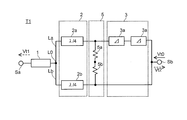
- FIG. 1 is a diagram showing an example of the configuration of the microwave rectification circuit according to the first embodiment.
- FIG. 2 is a view showing the configuration of a microwave rectification circuit according to Comparative Example 1.
- FIG. 3 is a diagram for explaining the operation of the microwave rectification circuit according to the first embodiment.
- FIG. 4 is a diagram showing the configuration of a first test circuit used for the first circuit simulation.
- FIG. 5 is a diagram showing simulation results of the first circuit simulation.
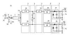
- FIG. 6 is a diagram showing the configuration of a second test circuit used for the second circuit simulation.
- FIG. 7 is a diagram showing the configuration of a comparison test circuit used for the second circuit simulation.
- 8A and 8B are diagrams showing simulation results of the second circuit simulation.
- FIG. 1 is a diagram showing an example of the configuration of the microwave rectification circuit according to the first embodiment.
- FIG. 2 is a view showing the configuration of a microwave rectification circuit according to Comparative Example 1.
- FIG. 3 is a diagram for
- FIG. 9 is a diagram illustrating an example of another aspect of the impedance matching unit and the phase shift unit.
- FIG. 10 is a diagram showing an example of the relationship between the circuit parameter of the circuit element of the ⁇ type circuit and the phase shift amount.
- FIG. 11 is a diagram showing an example of the configuration of the microwave rectification circuit according to the second embodiment.
- FIG. 12 is a diagram for explaining the operation of the microwave rectification circuit according to the second embodiment.
- FIG. 13 is a diagram showing an example of the configuration of the microwave rectification circuit according to the third embodiment.
- FIG. 1 is a view showing an example of the configuration of a microwave rectification circuit U according to the present embodiment.
- the microwave rectification circuit U includes an input line 1, an impedance matching unit 2, a phase shift unit 3, a rectification unit 4, and a branch resistance unit 5.
- the high frequency power received from the antenna A (hereinafter referred to as “input wave Vin”) is input to the input line 1.
- input wave Vin The high frequency power received from the antenna A
- branch lines La and Lb branched to a plurality from the branch point L0 are connected.
- the input wave Vin input to the input line 1 is branched from the branch point L0 to each of the plurality of branch lines La and Lb and travels to the subsequent stage side.
- the microwave rectification circuit U has a configuration in which the branch lines La and Lb are branched into two from the branch point L0.
- the branch line La will be referred to as “first branch line La”
- the branch line Lb will be referred to as “second branch line Lb”
- the configuration on the first branch line La is given the reference a and is referred to as “first... A”
- the configuration on the second branch line Lb is given the reference b. This will be described by referring to 2 of ... b ".
- the impedance matching unit 2 is disposed for each of the plurality of branch lines La and Lb, and performs impedance matching between the input line 1 and the subsequent stage.
- the impedance matching unit 2 according to the present embodiment is configured by ⁇ / 4 lines 2a and 2b.
- the ⁇ / 4 lines 2a and 2b are adjusted to a line length of ⁇ / 4 based on the wavelength ⁇ of the fundamental frequency of the input wave Vin.
- the first ⁇ / 4 line 2a is a transmission line constituting the first branch line La, and performs impedance matching between the input line 1 and the first rectifier 4a.
- the second ⁇ / 4 line 2b is a transmission line constituting the second branch line Lb, and performs impedance matching between the input line 1 and the second rectifier 4b.
- the first ⁇ / 4 line 2a and the second ⁇ / 4 line 2b also have a function of generating a 90 ° phase difference with respect to the passing input wave Vin (and the reflected wave).
- the first ⁇ / 4 line 2a and the second ⁇ / 4 line 2b perform impedance matching with the subsequent stage, thereby suppressing the reflection of the input wave Vin at the branch point L0.
- the impedance matching unit 2 can perform impedance matching and phase shift of 90 ° with the subsequent stage, any configuration such as a ⁇ -type circuit (described later with reference to FIG. 9) including an inductor and a capacitor May be realized by
- the phase shift unit 3 is disposed between the at least one impedance matching unit 2 of the plurality of branch lines La and Lb and the rectifying unit 4, and the synthesis of the fundamental wave component of the reflected wave generated by the rectifying unit 4 is a branch point
- the phase of the passing high frequency power is shifted so as to be zero at L0.
- the phase shift unit 3 causes the synthesis of the fundamental wave components of the reflected waves generated in the rectification unit 4 to be zero at the branch point L0.
- the potential of the wire connection position of 5 can be made zero (details will be described later).
- the phase shift unit 3 is constituted by the first phase shift unit 3a disposed in the subsequent stage of the first ⁇ / 4 line 2a, and the input wave Vin directed to the first rectification unit 4a is 90 ° phase shift (phase delay or phase lead).
- the first phase shift unit 3a also generates a 90 ° phase shift (phase delay or phase lead) for the reflected wave from the first rectifier 4a.
- the fundamental wave component of the reflected wave generated by the first rectification unit 4a and the fundamental wave component of the reflected wave generated by the second rectification unit 4b have the same waveform and a reverse phase at the branch point L0.
- the combination becomes zero at the branch point L0.
- the phase shift unit 3 is configured of, for example, a ⁇ / 4 line. However, the phase shift unit 3 may be realized by another configuration such as a delay circuit.
- the rectifying unit 4 is disposed downstream of the impedance matching unit 2 of each of the plurality of branch lines La and Lb to rectify the input wave Vin.
- the rectifying unit 4 is configured using a diode, and is configured of, for example, a single shunt type rectifying circuit or a voltage doubler type rectifying circuit.
- the first rectification unit 4a is connected to the subsequent stage of the first phase shift unit 3a of the first branch line La, and rectifies the input wave Vin output from the first phase shift unit 3a.
- the second rectification unit 4b is connected to the subsequent stage of the second ⁇ / 4 line 2b of the second branch line Lb, and rectifies the input wave Vin output from the second ⁇ / 4 line 2b.
- first rectifier 4a and the second rectifier 4b are configured to have the same reflection characteristics. Therefore, for example, a diode having the same characteristic and a circuit configuration of the same type are used for the first rectifier 4a and the second rectifier 4b.
- first reflected wave Vra the reflected wave generated by the first rectifier 4a
- second reflected wave Vrb the reflected wave generated by the second rectifier 4b
- the DC power generated by the first rectifier 4a and the DC power generated by the second rectifier 4b are both output to the current collector (not shown) in the subsequent stage, and are combined in the current collector. .
- the branch resistive portion 5 has a plurality of resistive portions 5a, 5b disposed to branch from the output end of the impedance matching portion 2 of each of the plurality of branch lines La, Lb, and the plurality of resistive portions 5a, 5b. The other ends of the two are connected to each other.
- the branch resistance unit 5 eliminates the reflected wave re-reflected or the like at the branch point L0 (details will be described later).
- one end of the first resistor portion 5a is connected to the output end of the first ⁇ / 4 line 2a, and one end of the first resistor portion 5b is the output of the second ⁇ / 4 line 2b.
- the other end of the first resistance portion 5a is connected to the other end of the second resistance portion 5b.
- first resistor portion 5a and the second resistor portion 5b is connected to the output end of the first ⁇ / 4 line 2a, and the other end is connected to the output end of the second ⁇ / 4 line 2b. It may be constituted by a single resistive element.
- a filter unit for example, an open stub that shields harmonics may be disposed upstream of the first rectifier unit 4a and the second rectifier unit 4b.
- FIG. 2 is a diagram showing the configuration of the microwave rectification circuit H1 according to Comparative Example 1. As shown in FIG.
- the microwave rectification circuit H1 according to the first comparative example includes the first branch line La and the second branch line Lb branched into two from the branch point L0 of the input line 1, and the first branch line La
- the first rectifier 4a is disposed via the first phase shift unit 3a, and the second rectifier 4b is directly connected to the branch point L0 on the second branch line Lb. .
- the microwave rectification circuit H1 In the microwave rectification circuit H1 according to Comparative Example 1, when the input wave Vin is input to the input line 1, first, the first reflected wave Vra is generated in the first rectifier 4a, and the second rectifier 4b is generated. The second reflected wave Vrb is generated at. At this time, the first reflected wave Vra and the second reflected wave Vrb each include a harmonic component in addition to the fundamental frequency component of the input wave Vin due to the non-linearity of the diode and the like. .
- the first reflected wave Vra and the second reflected wave Vrb have the same waveform because the reflection characteristic of the first rectifier 4a and the reflection characteristic of the second rectifier 4b are the same.
- the phase difference of 90 ° at the arrival time to the rectifying unit 4 with respect to the second reflected wave Vrb is obtained. It has become.
- the first reflected wave Vra passes through the phase shift unit 3a again to reach the branch point L0.
- the second reflected wave Vrb arrives at the branch point L0 as it is. Therefore, at the branch point L0, the first reflected wave Vra has a phase difference of 180 ° with respect to the second reflected wave Vrb. That is, at the branch point L0, the first reflected wave Vra and the second reflected wave Vrb have the same waveform, and their phases are reversed to each other. Therefore, the first reflected wave Vra and the second reflected wave Vrb cancel each other when traveling from the branch point L0 to the input line 1.
- the first rectification unit 4a and the second rectification unit 4b for dividing and inputting the input wave Vin are disposed, and the first rectification unit
- the phase shift unit 3a By arranging the phase shift unit 3a in the previous stage of one of the 4a or the second rectification unit 4b, it is possible to expect the canceling action of the reflected wave (the first reflected wave Vra and the second reflected wave Vrb) .
- the reflected wave can be reduced but can not be zero.
- the first reflected wave Vra returned to the branch point L0 is not all returned to the input line 1, and a part is re-reflected to the original first branch line La (hereinafter referred to as “A first re-reflected wave Vra1”, and another part of the second reentrant line Lb (hereinafter referred to as “a first wraparound reflected wave Vra2”).
- second re-reflected wave Vrb1 part of the second reflected wave Vrb returned to the branch point L0 is re-reflected to the original second branch line Lb (hereinafter referred to as “second re-reflected wave Vrb1”) Also, the other part flows into the other first branch line La (hereinafter, referred to as “second wraparound reflected wave Vrb2”).
- the reflected waves Vra1, Vra2, Vrb1, and Vrb2 re-reflected at the branch point L0 are reflected by the first rectifier 4a and the second rectifier 4b, respectively, and return to the branch point L0 again.
- the phases become in phase.
- the first wraparound reflected wave Vra2 and the second wraparound reflected wave Vrb2 return to the branch point L0, the phases become in phase.
- the reflected waves Vra1, Vra2, Vrb1, and Vrb2 are re-radiated from the antenna A from the input line 1 toward the antenna A without being canceled each other.
- the microwave rectification circuit U causes the branch resistance unit 5 to eliminate the reflected waves (Vra1, Vra2, Vrb1, Vrb2) re-reflected at the branch point L0.
- FIG. 3 is a diagram for explaining the operation of the microwave rectification circuit U according to the present embodiment.
- Vra is a first reflected wave generated in the first rectifier 4a
- Vrb is a second reflected wave generated in the second rectifier 4b
- Vra1 is a first re-reflected wave
- Vrb1 is a first reflected wave.
- the second re-reflected wave, Vra2 represents a first wraparound reflected wave
- Vrb2 represents a second wraparound reflected wave.
- the microwave rectification circuit U As in the microwave rectification circuit H1 according to the comparative example 1, the first reflected wave Vra is generated in the first rectification unit 4a, and the second rectification unit A second reflected wave Vrb is generated at 4b.
- the first reflected wave Vra returns to the branch point L0 via the first phase shift unit 3a and the first ⁇ / 4 line 2a.
- the second reflected wave Vrb returns to the branch point L0 via the second ⁇ / 4 line 2b.
- the first reflected wave Vra and a part of the second reflected wave Vrb return to the branch point L0, they flow into the branch resistance unit 5 and disappear.
- the behavior of the first reflected wave Vra and the second reflected wave Vrb at the branch point L0 is as described with reference to the microwave rectification circuit H1 according to the first comparative example. That is, a part of the first reflected wave Vra is re-reflected to the first ⁇ / 4 line 2a (a first re-reflected wave Vra1), and another part is reflected to the second ⁇ / 4 line 2b. (First wraparound reflected wave Vra2). Similarly, part of the second reflected wave Vrb is re-reflected to the second ⁇ / 4 line 2b (second re-reflected wave Vrb1), and the other part is reflected to the first ⁇ / 4 line 2a. Involvement (second wraparound reflected wave Vrb2).
- the microwave rectification circuit U since the branch resistance unit 5 is provided between the first and second rectification units 4a and 4b and the branch point L0, a known Wilkinson distributor and Similarly (see, for example, Non-Patent Document 1), the first re-reflected wave Vra1, the first wrap-around reflected wave Vra2, the second re-reflected wave Vrb1, and the second wrap-around reflected wave Vrb2 are The heat is absorbed by the branch resistor 5 from both ends of the branch resistor 5 and does not return to the first and second rectifiers 4a and 4b.
- the signals of the first reflected wave Vra and part of the second reflected wave Vrb propagate to the side of the input line 1 at the branch point L0, but these signals cancel each other out of phase. As a result, the reflected wave does not return to the input line 1 side.
- the microwave rectification circuit U since the reflected waves Vra1, Vra2, Vrb1, and Vrb2 re-reflected at the branch point L0 can be eliminated by the branch resistance unit 5, from the antenna A It is possible to suppress the occurrence of re-emission.
- the input wave Vin is in the same phase at both ends of the branch resistance portion 5 and therefore does not flow into the branch resistance portion 5 and does not become a loss in the branch resistance portion 5.
- the microwave rectification circuit U causes the branch resistance unit 5 to eliminate the reflected wave related to the odd-order harmonic component as well as the reflected wave of the fundamental frequency, and Return to the side can be reliably suppressed.
- the harmonic components generated as reflected waves in the first and second rectifiers 4a and 4b are usually only the odd-order harmonic components, so all the microwave rectification circuits U according to this embodiment are It can be said that the re-radiation from the antenna A is also suppressed with respect to the harmonic components of Also, in order to completely cut off even-order harmonics, by installing a corresponding cut-off filter using a stub or the like, it is possible to realize without degrading the characteristics of the rectenna circuit.
- the following equation (1) is set to hold.
- (2 ⁇ Z 1 ) ⁇ Z 3 Z 2 2 (1) (However, Z 1 : characteristic impedance of input line 1 [ ⁇ ], Z 2 : characteristic impedance of first ⁇ / 4 line 2 a [ ⁇ ], Z 3 : subsequent stage of first ⁇ / 4 line 2 a (first Characteristic impedance [ ⁇ ]) of the phase shift unit 3a etc.
- the reason that the characteristic impedance of the input line 1 is (2 ⁇ Z 1 ) is because the first ⁇ / 4 line 2 a is one side branched into two.
- the characteristic impedance of the second lambda / 4 line 2b is also set to be the same characteristic impedance Z 2 and the first lambda / 4 line 2a.
- Resistance Z 4 of the first resistor portion 5a of the branch resistor section 5 (and the second resistor portion 5b) is reflected wave Vra1 re reflection or the like at the branch point L0, Vra2, Vrb1, Vrb2 is first ⁇ It sets so that it may go to the connection position of the said branch resistance part 5, without reflecting in the connection position with the / 4 track
- the input wave Vin because the same phase on both sides of the branch resistor section 5, because the flow to the branch resistor unit 5 does not occur, when setting the resistance value Z 4 of the first resistor portion 5a Can be ignored and considered.
- the resistance value Z 4 of the first resistor portion 5a is reflected wave Vra1 re reflection or the like at the branch point L0, Vra2, Vrb1, Vrb2 only may be set in consideration.
- the potential at the connection position of the branch resistance unit 5 is zero [V].
- the impedance on the side of the first phase shift unit 3a can also be ignored. That is, the condition that the first re-reflected wave Vra1 and the second wraparound reflected wave Vrb2 are absorbed by the first resistance portion 5a without being reflected at the connection position of the first resistance portion 5a is the first condition.
- resistance Z 4 of the resistor portion 5a is that the characteristic impedance of the first lambda / 4 line 2a and (Z 2) are impedance matched.
- the resistance value Z 4 of the first resistor portion 5a from the general lambda / 4 line condition of impedance matching, set to satisfy the following equation (2).
- (2 ⁇ Z 1 ) ⁇ Z 4 Z 2 2 (2) (Where Z 1 : characteristic impedance of input line 1 [ ⁇ ], Z 2 : characteristic impedance of first ⁇ / 4 line 2 a [ ⁇ ], Z 4 : resistance value of first resistor portion 5 a [ ⁇ ])
- the resistance value Z 4 of the first resistor portion 5a may be set to be the same value as the characteristic impedance Z 3 of the first phase shift unit 3a.
- the reflected waves Vra1, Vra2, Vrb1, and Vrb2 re-reflected at the branch point L0 are obtained.
- FIG. 4 is a diagram showing the configuration of the first test circuit T1 used for the first circuit simulation.
- the first circuit simulation observes the behavior of the first and second reflected waves Vra and Vrb generated by the first and second rectifiers 4a and 4b of the microwave rectification circuit U according to the present embodiment.
- a high frequency signal Vt0 simulating the first and second reflected waves Vra and Vrb is input from the port Sb, and the amount of transmission of the high frequency signal Vt0 to the port Sa is detected.
- two first phase shift portions 3a are continuously arranged on the first branch line La side, and thereby, have a phase difference of 180 ° from the high frequency signal Vt0.
- a first reflected wave Vra and a second reflected wave Vrb are generated.
- the input line 1, the first ⁇ / 4 line 2a, the second ⁇ / 4 line 2b, the phase shift unit 3, and the branch resistance unit 5 in FIG. 4 are respectively the microwave rectification circuit of FIG. It has the same configuration as each configuration of U.
- the first ⁇ / 4 line 2a, the second ⁇ / 4 line 2b, the first phase shift unit 3a, and the branch resistance unit 5 with reference to 5.8 GHz (fundamental frequency) Impedance etc. is set. Then, in the first circuit simulation, a signal component Vt1, a signal component Vt2 and a loss Pt when the frequency of the high frequency signal Vt0 is changed are calculated. In other words, this circuit simulation verifies the behavior of each frequency in the microwave rectification circuit U in which 5.8 GHz is set as the fundamental frequency.
- FIG. 5 is a diagram showing simulation results of the first circuit simulation.
- Vt1 (dotted line) is the magnitude of the signal component transmitted to the port Sa
- Vt2 (dashed dotted line) is the magnitude of the signal component re-reflected to the port Sb
- Pt (solid line) is the branch resistance portion Power loss at 5 is shown.
- the horizontal axis represents frequency [GHz]
- the vertical axis represents the magnitude of Vt1, Vt2 and Pt when the input component is 1.
- FIG. 6 is a diagram showing the configuration of a second test circuit T2 used for the second circuit simulation.
- FIG. 7 is a diagram showing the configuration of the comparison test circuit H2 used for the second circuit simulation.
- the test circuit H2 for comparison is a microwave rectification circuit according to the prior art that performs a rectification operation without branching from the input line 1.
- the high frequency signal Vt3 is input from the input port Sc, and the DC output Vt4 detected at the output port Sd and the power Vt5 of the reflected wave reflected to the input line 1 detected at the detection port Se are detected. Do.
- Each of the branch resistance portions 5 has the same configuration as that shown in FIG. However, here, the filter unit 6 (the first filter unit 6a, the second filter unit 6b) for shielding the reflected waves of harmonics in the front stage of the first rectifier unit 4a and the second rectifier unit 4b. are provided.
- the resistors 7a and 7b in FIGS. 6 and 7 are power loads, the capacitor 8 is a capacitor for cutting a direct current, and the circulator 9 is a configuration for detecting a reflected wave reflected to the input line 1.
- the second test circuit T2 and the comparison test circuit H2 are adjusted by the first filter unit 6a, the second filter unit 6b, etc. It is set so that reflection in the 1st rectification part 4a and the 2nd rectification part 4b may become the minimum.
- FIG. 8 is a diagram showing a simulation result of the second circuit simulation.
- FIG. 8A shows a simulation result of the second test circuit T2
- FIG. 8B shows a simulation result of the comparison test circuit H2.
- Pd2 (dotted line) indicates the power loss in the rectifying unit 4
- Pr2 (solid line) indicates the reflected power detected by the circulator 9.
- the horizontal axis Pin represents the input power (10 mW to 10 W) [W]
- the vertical axis the magnitude of the power loss Pd2 (dotted line) when the input component is 1
- the reflected power Pr2 (solid line) Represents the size of
- both the reflected power Pr2 and the power loss Pd2 are large even when the input power at which the shielding effect of the reflected wave of the filter unit 6 is exhibited is 1 W. It is observed.
- the reflected power Pr2 is substantially zero regardless of the input power Pin.
- the microwave rectification circuit U As described above, according to the microwave rectification circuit U according to the present embodiment, the reflected waves (Vra, Vrb) generated by the rectifying unit 4 cancel each other at the branch point L0, and the reflected waves re-reflected at the branch point L0
- the (Vra1, Vra2, Vrb1, Vrb2) can be eliminated by the branch resistor 5.
- the microwave rectification circuit U concerning this embodiment can exhibit the said effect also about a harmonic component in addition to fundamental frequency. Therefore, the microwave rectification circuit U according to the present embodiment can reliably suppress the re-radiation of the received microwaves from the antenna A to the external space during the rectification operation.
- the reflected wave re-reflected at the branch point L0 is not input to the first rectifier 4a, the second rectifier 4b, etc. It is possible to operate stably even in the performance limit of the first rectifier 4a and the second rectifier 4b. As a result, it contributes to the improvement of the conversion efficiency of RF / DC.
- the configuration is shown in which the branch point L0 is branched into two, the first branch line La and the second branch line Lb, but the configuration may be modified to form a plurality of sets, etc. .
- branch lines L0 to 2 ⁇ m (m is an arbitrary positive integer) number of branch lines are branched, one m branch lines and another m branch lines are connected to the rectifying unit 4
- the phase of the input wave Vin may be shifted so as to have a phase difference of 90.degree.
- line respectively was shown.
- the impedance matching unit 2 and the phase shift unit 3 may be realized by other circuit configurations.
- FIG. 9 is a diagram showing an example of another circuit configuration of the impedance matching unit 2 or the phase shift unit 3.
- the circuit shown in FIG. 9 is a ⁇ -type circuit, and includes an inductance element L1, a first capacitor C1, and a second capacitor C2.
- the inductance element L1 is connected in series between the input side and the output side, and the first capacitor C1 is connected to the front stage of the inductance element L1 with one end grounded, and the second capacitor C2 is In the state where one end is grounded, it is connected to the latter stage of the inductance element L1.
- the impedance on the signal source side is conjugate to the impedance on the load side with respect to the input point of the impedance matching circuit, and the impedance on the signal source side is based on the output point of the impedance matching circuit. It can be realized by setting the circuit constant of the circuit element so as to have a conjugate relationship with the impedance on the side.
- the input line for high frequency power of the microwave band is obtained. It is possible to perform impedance matching between the first and second rectifiers 4.
- FIG. 10 shows the phase shift amount and the circuit parameter (the inductor of the inductance element L1, the capacitance of the first capacitor C1 and the second capacitor C2) of the circuit element of the ⁇ type circuit when the high frequency power is 5.8 GHz. It is a figure which shows an example of the relationship of.
- the ⁇ circuit can adjust the amount of phase shift of the passing high frequency power by appropriately setting the capacitance of the inductor of the inductance element L1, the first capacitor C1 and the second capacitor C2. it can.
- the impedance matching unit 2 using a lumped constant line like a ⁇ -type circuit differs in delay time with respect to the fundamental wave and delay time with respect to the harmonics, the reflection suppressing effect due to the phase difference to the harmonics can not be expected.
- the transmittance for high frequency is lowered, harmonic reflection is also suppressed as a result. To suppress more completely. What is necessary is just to insert the cutoff filter to a harmonic.
- FIG. 11 is a view showing an example of the configuration of a microwave rectification circuit U according to the second embodiment.
- the microwave rectification circuit U is configured to branch into three branch lines La, Lb, and Lc from a branch point L0.
- the description of the configuration common to the first embodiment will be omitted (the same applies to the other embodiments hereinafter).
- the branch line La is referred to as “first branch line La”, the branch line Lb as “second branch line Lb”, and the branch line Lc as “third branch line Lc”.
- first branch line La the configuration on the branch lines La, Lb, and Lc is distinguished and described
- the configuration on the first branch line La is given the symbol a and is referred to as "first ... a”
- second... B the configuration on the branch line Lb
- the configuration on the third branch line Lb is denoted by the symbol c and "third ... c" It is called and explained.
- the first rectifier 4a is connected to the first branch line La via the first ⁇ / 4 line 2a.
- the second rectifier 4b is connected to the second branch line Lb via the second ⁇ / 4 line 2b and the second phase shift unit 3b.
- the third rectifying unit 4c is connected to the third branch line Lc via the third ⁇ / 4 line 2c and the third phase shift unit 3c.
- the branch resistance unit 5 is connected to the output end of the first ⁇ / 4 line 2a, the output end of the second ⁇ / 4 line 2b, and the output end of the third ⁇ / 4 line 2c.
- Y connection is made via the second and third resistance portions 5a, 5b, 5c.
- the first ⁇ / 4 line 2a, the second ⁇ / 4 line 2b, and the third ⁇ / 4 line 2c are between the input line 1 and the subsequent stage, as in the first embodiment. Impedance matching. Further, each of the first rectifier 4a, the second rectifier 4b, and the third rectifier 4c also forms a rectifier circuit having equivalent reflection characteristics, as in the first embodiment.
- the second phase shift unit 3b shifts the phase of the high frequency power passing therethrough by 60 ° (phase delay or phase lead).
- the phase shift unit 3c of 3 shifts the phase of the high frequency power passing therethrough by 120 ° (phase delay or phase lead).
- the first reflected wave Vra generated in the first rectifier 4a, the second reflected wave Vrb generated in the second rectifier 4b, and the third reflected wave Vrc generated in the third rectifier 4c At the branch point L0, each has the same waveform and a phase difference of 120 °.
- the first reflected wave Vra, the second reflected wave Vrb, and the third reflected wave Vrc are made to be in a three-phase alternating current state at the branch point L0. Cancel each other out.
- the microwave rectification circuit U since the first reflected wave Vra, the second reflected wave Vrb, and the third reflected wave Vrc re-reflect, etc. at the branch point L0, they disappear. In order to do this, the branch resistance unit 5 is provided.
- FIG. 12 is a diagram for explaining the operation of the microwave rectification circuit U according to the present embodiment.
- the first reflected wave Vra returns to the first branch line La at the branch point L0 due to rereflection, and also enters the first branch line Lb and the third branch line Lc. Generates a wraparound reflected wave Vra2. Also, the second reflected wave Vrb wraps around the second re-reflected wave Vrb1 returning to the second branch line Lb due to re-reflection and the first branch line La and the third branch line Lc at the branch point L0. A second wraparound reflected wave Vrb2 is generated.
- the third reflected wave Vrc wraps around the third rereflection wave Vrc1 that returns to the third branch line Lc due to rereflection at the branch point L0, and the first branch line La and the second branch line Lb.
- a third wraparound reflected wave Vrc2 is generated.
- a part of the signal propagates to the input line 1 side at the branch point L0, and this signal has a first reflected wave Vra, a second reflected wave Vrb, and a third reflected wave Vrc of 120 ° to each other. They have a phase difference and cancel each other out because they have the same amplitude. As a result, the reflected wave does not return to the input side.
- the first resistor portion 5a (the second resistance portion 5b, the third resistance portion 5c) resistance Z 4 of the impedance matching of the lambda / 4 line than conditional expression of the following It sets so that Formula (3) may be satisfied.
- (3 ⁇ Z 1 ) ⁇ Z 4 Z 2 2 (3) (Where Z 1 is the characteristic impedance of the input line 1, Z 2 is the characteristic impedance of the first ⁇ / 4 line 2a, and Z 4 is the resistance value of the first resistor portion 5a)
- the microwave rectification circuit U As described above, according to the microwave rectification circuit U according to the present embodiment, the reflected waves (Vra, Vrb, Vrc) generated in the rectifying unit 4 are mutually canceled at the branch point L0, and re-reflection or the like is performed at the branch point L0.
- the reflected wave (Vra1, Vra2, Vrb1, Vrb2, Vrc1, Vrc2) can be eliminated by the branch resistance unit 5. Therefore, the microwave rectification circuit U according to the present embodiment can reliably suppress re-radiation from the antenna A to the external space.
- FIG. 13 is a view showing an example of the configuration of a microwave rectification circuit U according to the third embodiment.
- the microwave rectification circuit U is configured to branch from the branch point L0 to n branch lines Ln1, Ln2, Ln3 ⁇ Lnn.
- the phase shift unit 3 shifts the phase of high frequency power input to the branch lines Ln1, Ln2, Ln3 ⁇ Lnn by 180 / n ° (phase delay or phase lead).
- the high frequency powers flowing through the n-1 branch lines Ln2, Ln2, Ln3... Lnn are different from the high frequency powers flowing through one branch line Ln1 when reaching the rectifying unit 4 respectively.
- they have different phase differences by k ⁇ 180 / n ° (k is a positive integer of 1 to n ⁇ 1).
- the synthesis of the reflected waves generated in the rectifying unit 4 can be made zero at the branch point L0. Then, when the synthesis of the reflected waves generated in the rectifying unit 4 becomes zero at the branch point L0, as described in the first and second embodiments, from the reflected wave re-reflected at the branch point L0, etc.
- the connection position of the branch resistance unit 5 is in a state where the potential is zero.
- the reflected wave re-reflected at the branch point L0 is absorbed by the branch resistance portion 5 and disappears.
- the resistance value Z 4 of the resistance portion 5n1 branch resistor section 5, from the conditional expression of the impedance matching of the lambda / 4 line is set so as to satisfy the following equation (4).
- N ⁇ Z 1 ) ⁇ Z 4 Z 2 2 (4) (Where Z 1 : characteristic impedance of input line 1, Z 2 : characteristic impedance of ⁇ / 4 line 2 n 1, Z 4 : resistance value of resistance section 5 n 1)
- the phase of the high frequency power flowing through the n branch lines is shifted by 180 / n ° as an example of the phase shift unit 3.
- the high frequency power having the same phase A configuration may be adopted in which a plurality of branched lines to be flowed are set as a set, and the phase shift amount is set in units of the set.
- microwave rectification circuit According to the microwave rectification circuit according to the present disclosure, re-radiation from the antenna to the external space can be reliably suppressed.
Landscapes
- Engineering & Computer Science (AREA)
- Power Engineering (AREA)
- Rectifiers (AREA)
Abstract
交流電力を整流するマイクロ波整流回路であって、入力線路(1)の出力側の分岐点から複数に分岐する分岐線路と、複数の前記分岐線路それぞれに配設されたインピーダンス整合部(2)と、複数の前記分岐線路それぞれの前記インピーダンス整合部(2)の後段に配設されて、前記交流電力を整流する整流部(4)と、複数の前記分岐線路の少なくとも一の前記インピーダンス整合部(2)と前記整流部(4)の間に配設され、前記整流部(4)で発生する反射波の基本波成分の合成が前記分岐点においてゼロとなるように、前記交流電力の位相をシフトする位相シフト部(3)と、複数の前記分岐線路それぞれの前記インピーダンス整合部(2)の出力端から分岐するように配設された複数の抵抗部を有し、当該複数の抵抗部の他端を互いに結線して構成される分岐抵抗部(5)と、を備える。
Description
本開示は、マイクロ波整流回路に関する。
アンテナでマイクロ波帯域の電磁波を受電し、得られた高周波電力を整流して直流電力に変換(RF-DC変換)するレクテナ装置(Rectifying Antenna:レクチファイア・アンテナとも称される)が知られている(例えば、特許文献1や特許文献2を参照)。
この種のレクテナ装置で使用される整流回路(以下、「マイクロ波整流回路」と称する)においては、当該マイクロ波整流回路内からアンテナ側への反射波を抑制する要請がある。
一般に、高周波電力が使用される回路においては、回路間の接続部でインピーダンスが異なると反射波が起こる。そして、マイクロ波整流回路において、アンテナ側への反射波が発生した場合、当該反射波は、アンテナから外部空間へ再放射され、電力損失の増大を引き起こし、加えて、他の用途の電波への悪影響を及ぼすことにもなる。
又、マイクロ波整流回路においては、整流ダイオードの非線形性に起因して、基本周波数の反射波に加えて、高調波の反射波も発生する。マイクロ波整流回路においては、通流する電力が無線通信に比べて遙かに大きいため、基本周波数の反射波に加えて、当該高調波の反射波の抑制も求められる。
小西 良弘,「実用マイクロ波技術講座―理論と実際〈第2巻〉」,ケイラボ出版,2001,PP.56-58
かかる問題を解決するため、例えば、特許文献1には、整流ダイオードからなる整流部の前段に、フィルタとオープンスタブを配設することが記載されている。そして、特許文献1の従来技術においては、フィルタによって高調波の反射波を遮蔽し、当該フィルタを通過してくる基本波成分の反射波をオープンスタブ等で遮蔽する。
しかしながら、特許文献1の従来技術においては、レクテナ装置に伝送される電磁波の伝搬態様や整流部内で発生する反射波が一定であることが前提となっている。一方、電磁波の伝搬態様は、実際には大きく変化する。又、整流部における反射特性は、例えば、入力電力や出力電力等、レクテナ装置の使用条件に応じて大きく変化する。そのため、特許文献1の従来技術においては、アンテナ側への反射波を抑制することは、実際には困難な場合が多い。
本開示は、上記の問題点に鑑みてなされたもので、整流動作の際に、受電したマイクロ波がアンテナから外部空間へ再放射されることを確実に抑制し得るマイクロ波整流回路を提供することを目的とする。
前述した課題を解決する主たる本開示は、
交流電力を整流するマイクロ波整流回路であって、
前記交流電力が入力される入力線路と、
前記入力線路の出力側の分岐点から複数に分岐する分岐線路と、
複数の前記分岐線路それぞれに配設されて、前記入力線路と後段との間でインピーダンス整合と90°の位相シフトを行うインピーダンス整合部と、
複数の前記分岐線路それぞれの前記インピーダンス整合部の後段に配設されて、前記交流電力を整流する整流部と、
複数の前記分岐線路の少なくとも一の前記インピーダンス整合部と前記整流部の間に配設され、前記整流部で発生する反射波の基本波成分の合成が前記分岐点においてゼロとなるように、前記交流電力の位相をシフトする位相シフト部と、
複数の前記分岐線路それぞれの前記インピーダンス整合部の出力端から分岐するように配設された複数の抵抗部を有し、当該複数の抵抗部の他端を互いに結線して構成される分岐抵抗部と、
を備える、マイクロ波整流回路。
交流電力を整流するマイクロ波整流回路であって、
前記交流電力が入力される入力線路と、
前記入力線路の出力側の分岐点から複数に分岐する分岐線路と、
複数の前記分岐線路それぞれに配設されて、前記入力線路と後段との間でインピーダンス整合と90°の位相シフトを行うインピーダンス整合部と、
複数の前記分岐線路それぞれの前記インピーダンス整合部の後段に配設されて、前記交流電力を整流する整流部と、
複数の前記分岐線路の少なくとも一の前記インピーダンス整合部と前記整流部の間に配設され、前記整流部で発生する反射波の基本波成分の合成が前記分岐点においてゼロとなるように、前記交流電力の位相をシフトする位相シフト部と、
複数の前記分岐線路それぞれの前記インピーダンス整合部の出力端から分岐するように配設された複数の抵抗部を有し、当該複数の抵抗部の他端を互いに結線して構成される分岐抵抗部と、
を備える、マイクロ波整流回路。
本開示に係るマイクロ波整流回路によれば、整流動作の際に、受電したマイクロ波がアンテナから外部空間へ再放射されることを確実に抑制することができる。
以下に添付図面を参照しながら、本開示の好適な実施の形態について詳細に説明する。尚、本明細書及び図面において、実質的に同一の機能構成を有する構成要素については、同一の符号を付することにより重複説明を省略する。
(第1の実施形態)
[マイクロ波整流回路の構成]
以下、図1を参照して、第1の実施形態に係るマイクロ波整流回路Uの構成の一例について説明する。本実施形態に係るマイクロ波整流回路Uは、例えば、上記したレクテナ装置に適用される。
[マイクロ波整流回路の構成]
以下、図1を参照して、第1の実施形態に係るマイクロ波整流回路Uの構成の一例について説明する。本実施形態に係るマイクロ波整流回路Uは、例えば、上記したレクテナ装置に適用される。
図1は、本実施形態に係るマイクロ波整流回路Uの構成の一例を示す図である。
本実施形態に係るマイクロ波整流回路Uは、入力線路1、インピーダンス整合部2、位相シフト部3、整流部4、及び分岐抵抗部5を備えている。
入力線路1には、アンテナAから受電した高周波電力(以下、「入力波Vin」と称する)が入力される。入力線路1の出力側には、分岐点L0から複数に分岐する分岐線路La、Lbが接続されている。入力線路1に入力された入力波Vinは、分岐点L0から、複数の分岐線路La、Lbそれぞれに分岐して後段側に向かう。
尚、本実施形態に係るマイクロ波整流回路Uは、分岐点L0から分岐線路La、Lbが二股に分岐する構成となっている。本実施形態では、分岐線路Laを「第1の分岐線路La」、分岐線路Lbを「第2の分岐線路Lb」と称すると共に、いずれの分岐線路La、Lb上の構成かを区別して説明する際には、第1の分岐線路La上の構成については符号aを付して「第1の…a」と称し、第2の分岐線路Lb上の構成については符号bを付して「第2の…b」と称して説明する。
インピーダンス整合部2は、複数の分岐線路La、Lbそれぞれに配設されて、入力線路1と後段との間でインピーダンス整合を行う。本実施形態に係るインピーダンス整合部2は、λ/4線路2a、2bによって、構成されている。λ/4線路2a、2bは、入力波Vinの基本周波数の波長λに基づいて、λ/4の線路長に調整されている。
具体的には、第1のλ/4線路2aは、第1の分岐線路Laを構成する伝送線路であって、入力線路1と第1の整流部4aの間のインピーダンス整合を行う。又、第2のλ/4線路2bは、第2の分岐線路Lbを構成する伝送線路であって、入力線路1と第2の整流部4bの間のインピーダンス整合を行う。尚、第1のλ/4線路2a及び第2のλ/4線路2bは、通過する入力波Vin(及び反射波)に対して、90°位相差を発生させる機能も有する。
第1のλ/4線路2a及び第2のλ/4線路2bが、後段とのインピーダンス整合を行うことによって、入力波Vinが分岐点L0において、反射することを抑制する。但し、インピーダンス整合部2は、後段との間でインピーダンス整合と90°の位相シフトを行うことができれば、インダクタとキャパシタで構成したπ型回路(図9を参照して後述)等、任意の構成によって実現されてよい。
位相シフト部3は、複数の分岐線路La、Lbの少なくとも一のインピーダンス整合部2と整流部4の間に配設され、整流部4で発生する反射波の基本波成分の合成が、分岐点L0においてゼロとなるように、通過する高周波電力の位相をシフトする。尚、位相シフト部3が、整流部4で発生する反射波の基本波成分の合成が分岐点L0においてゼロとなるようにすることで、再反射等した反射波から見たとき、分岐抵抗部5の結線位置の電位をゼロの状態とすることができる(詳細は後述)。
本実施形態においては、位相シフト部3は、第1のλ/4線路2aの後段に配設された第1の位相シフト部3aによって構成され、第1の整流部4aに向かう入力波Vinを90°位相シフト(位相遅れ又は位相進み)する。又、第1の位相シフト部3aは、第1の整流部4aからの反射波に対しても90°の位相シフト(位相遅れ又は位相進み)を発生させる。これによって、第1の整流部4aで発生する反射波の基本波成分と第2の整流部4bで発生する反射波の基本波成分とは、分岐点L0において、同一波形で且つ逆位相の関係となり、当該分岐点L0において、その合成はゼロとなる。
位相シフト部3は、例えば、λ/4線路によって構成される。但し、位相シフト部3は、遅延回路等、他の構成によって実現されてよい。
整流部4は、複数の分岐線路La、Lbそれぞれのインピーダンス整合部2の後段に配設されて、入力波Vinを整流する。整流部4は、ダイオードを用いて構成され、例えば、シングルシャント型の整流回路、ボルテージダブラ型の整流回路によって構成される。
具体的には、第1の整流部4aは、第1の分岐線路Laの第1の位相シフト部3aの後段に接続され、第1の位相シフト部3aから出力される入力波Vinを整流する。第2の整流部4bは、第2の分岐線路Lbの第2のλ/4線路2bの後段に接続され、第2のλ/4線路2bから出力される入力波Vinを整流する。
但し、第1の整流部4aと第2の整流部4bとは、同一の反射特性を有するように構成される。そのため、第1の整流部4aと第2の整流部4bとは、例えば、同一特性のダイオード、及び同一種別の回路構成が用いられる。これによって、第1の整流部4aで発生する反射波(以下、「第1の反射波Vra」と称する)と第2の整流部4bで発生する反射波(以下、「第2の反射波Vrb」と称する)とが同一波形となる。
第1の整流部4aが生成した直流電力と、第2の整流部4bが生成した直流電力は、共に、後段の集電部(図示せず)に出力され、当該集電部において合成される。
分岐抵抗部5は、複数の分岐線路La、Lbそれぞれのインピーダンス整合部2の出力端から分岐するように配設された複数の抵抗部5a、5bを有し、当該複数の抵抗部5a、5bの他端を互いに結線して構成されている。分岐抵抗部5は、分岐点L0において再反射等した反射波を消滅させる(詳細は後述)。
具体的には、第1の抵抗部5aは、一端が第1のλ/4線路2aの出力端に接続され、第2の抵抗部5bは、一端が第2のλ/4線路2bの出力端に接続され、第1の抵抗部5aの他端と第2の抵抗部5bの他端とが結線されている。
尚、第1の抵抗部5a及び第2の抵抗部5bは、一端が第1のλ/4線路2aの出力端に接続され、他端が第2のλ/4線路2bの出力端に接続された一個の抵抗素子によって構成されてもよい。
尚、マイクロ波整流回路Uには、第1の整流部4a及び第2の整流部4bそれぞれの前段に高調波を遮蔽するフィルタ部(例えば、オープンスタブ)が配設されてもよい。
[マイクロ波整流回路の動作]
以下、図2~図3を参照して、本実施形態に係るマイクロ波整流回路Uの動作について説明する。
以下、図2~図3を参照して、本実施形態に係るマイクロ波整流回路Uの動作について説明する。
図2は、比較例1に係るマイクロ波整流回路H1の構成を示す図である。
まず、比較例1に係るマイクロ波整流回路H1を参照して、入力波Vinを入力線路1から分岐させることによる反射波(第1の反射波Vraと第2の反射波Vrb)の相殺作用について説明する。
比較例1に係るマイクロ波整流回路H1は、入力線路1の分岐点L0から二股に分岐した第1の分岐線路Laと第2の分岐線路Lbとを有し、第1の分岐線路Laには、第1の位相シフト部3aを介して第1の整流部4aが配設され、第2の分岐線路Lbには、第2の整流部4bが分岐点L0に直結された構成となっている。
比較例1に係るマイクロ波整流回路H1において、入力波Vinが入力線路1に入力されると、まず、第1の整流部4aにおいて第1の反射波Vraが発生し、第2の整流部4bにおいて第2の反射波Vrbが発生する。この際、ダイオードの非線形性等に起因して、第1の反射波Vraと第2の反射波Vrbは、それぞれ、入力波Vinの基本周波数成分に加えて高調波成分を含むものとなっている。
但し、第1の反射波Vraと第2の反射波Vrbは、第1の整流部4aの反射特性と第2の整流部4bの反射特性とが同一であるため、同一波形となっている。又、第1の反射波Vraは、入力波Vinが位相シフト部3を介して入力されるため、第2の反射波Vrbに対して、整流部4への到着時点で90°の位相差を有するものとなっている。
第1の反射波Vraは、再度、位相シフト部3aを通過して、分岐点L0に到達する。一方、第2の反射波Vrbは、そのまま、分岐点L0に到達する。従って、分岐点L0においては、第1の反射波Vraは、第2の反射波Vrbに対して、180°の位相差を有することになる。つまり、分岐点L0においては、第1の反射波Vraと第2の反射波Vrbは、同一波形で、互いに位相が反転した状態となっている。従って、第1の反射波Vraと第2の反射波Vrbとは、分岐点L0から入力線路1に向かう際に互いに打ち消し合うことになる。
このように、比較例1に係るマイクロ波整流回路H1においては、入力波Vinを分岐して入力する第1の整流部4aと第2の整流部4bを配設すると共に、第1の整流部4a又は第2の整流部4bの一方の前段に位相シフト部3aを配設することによって、反射波(第1の反射波Vraと第2の反射波Vrb)の相殺作用を期待することができる。
しかしながら、比較例1に係るマイクロ波整流回路H1においては、反射波を減少はできてもゼロにすることはできない。
詳述すると、分岐点L0に戻ってきた第1の反射波Vraは、すべてが入力線路1に戻るわけではなく、一部は、元来た第1の分岐線路Laに再反射し(以下、「第1の再反射波Vra1」と称する)、又、他の一部はもう一方の第2の分岐線路Lbへ回り込む(以下、「第1の回り込み反射波Vra2」と称する)。
同様に、分岐点L0に戻ってきた第2の反射波Vrbは、一部は、元来た第2の分岐線路Lbに再反射し(以下、「第2の再反射波Vrb1」と称する)、又、他の一部はもう一方の第1の分岐線路Laへ流れ込む(以下、「第2の回り込み反射波Vrb2」と称する)。
分岐点L0において再反射等した反射波Vra1、Vra2、Vrb1、Vrb2は、それぞれ、第1の整流部4aと第2の整流部4bにおいて反射し、再び分岐点L0に戻ってくる。第1の再反射波Vra1と第2の再反射波Vrb1は、再び分岐点L0に戻ってくる際には、位相がそろった状態となる。又、第1の回り込み反射波Vra2と第2の回り込み反射波Vrb2も、同様に、分岐点L0に戻ってくる際には、位相がそろった状態となる。その結果、当該反射波Vra1、Vra2、Vrb1、Vrb2は、互いに打ち消されることなく、入力線路1からアンテナA側に向かい、アンテナAから再放射されることになる。
本実施形態に係るマイクロ波整流回路Uは、上記に鑑みて、分岐点L0において再反射等した反射波(Vra1、Vra2、Vrb1、Vrb2)を分岐抵抗部5によって消失させる。
図3は、本実施形態に係るマイクロ波整流回路Uの動作を説明する図である。
図3中において、Vraは第1の整流部4aにおいて発生する第1の反射波、Vrbは第2の整流部4bにおいて発生する第2の反射波、Vra1は第1の再反射波、Vrb1は第2の再反射波、Vra2は第1の回り込み反射波、Vrb2は第2の回り込み反射波を表す。
本実施形態に係るマイクロ波整流回路Uにおいても、上記比較例1に係るマイクロ波整流回路H1と同様に、第1の整流部4aにおいて第1の反射波Vraが発生し、第2の整流部4bにおいて第2の反射波Vrbが発生する。
第1の反射波Vraは、第1の位相シフト部3a及び第1のλ/4線路2aを介して、分岐点L0に戻ってくる。又、第2の反射波Vrbは、第2のλ/4線路2bを介して、分岐点L0に戻ってくる。尚、第1の反射波Vraと第2の反射波Vrbの一部は、分岐点L0に戻ってくる際に、分岐抵抗部5へ流れ込んで消失する。
分岐点L0における第1の反射波Vra及び第2の反射波Vrbの挙動は、比較例1に係るマイクロ波整流回路H1を参照して説明した通りである。つまり、第1の反射波Vraは、一部が第1のλ/4線路2aに再反射し(第1の再反射波Vra1)、他の一部が第2のλ/4線路2bに回り込む(第1の回り込み反射波Vra2)。同様に、第2の反射波Vrbは、一部が第2のλ/4線路2bに再反射し(第2の再反射波Vrb1)、他の一部が第1のλ/4線路2aに回り込む(第2の回り込み反射波Vrb2)。
この際、本実施形態に係るマイクロ波整流回路Uにおいては、第1及び第2の整流部4a、4bと分岐点L0の間に分岐抵抗部5を設けているため、公知のウィルキンソン分配器と同様に(詳細には、例えば、非特許文献1を参照)、第1の再反射波Vra1、第1の回り込み反射波Vra2、第2の再反射波Vrb1、及び第2の回り込み反射波Vrb2は、分岐抵抗部5の両端から当該分岐抵抗部5に吸収されて熱となり、第1及び第2の整流部4a、4bの方へは戻らない。又、第1の反射波Vraと第2の反射波Vrbの一部の信号は、分岐点L0点で入力線路1側に伝搬するが、この信号は逆相のため互いに打ち消し合う。その結果、入力線路1側にも反射波は戻らない。
このように、本実施形態に係るマイクロ波整流回路Uにおいては、分岐点L0において再反射等した反射波Vra1、Vra2、Vrb1、Vrb2を分岐抵抗部5で消失させることができるため、アンテナAから再放射が発生することを抑制することができる。
尚、入力波Vinについては、分岐抵抗部5の両端で、同位相であるため、当該分岐抵抗部5への流れ込みは生じず、当該分岐抵抗部5における損失とはならない。
以上では、基本周波数の反射波についてのみ説明したが、基本周波数の第1及び第2の反射波Vra、Vrbにおいて位相差が180°となる場合には、2n+1(nは任意の正の整数)で表される奇数次の高調波においても、同様に、位相差は180°+n×360°となる。従って、本実施形態に係るマイクロ波整流回路Uは、奇数次の高調波成分に係る反射波についても、基本周波数の反射波と同様に、分岐抵抗部5において消失させ、入力線路1からアンテナA側に戻ることを確実に抑制することができる。
尚、第1及び第2の整流部4a、4bにおいて反射波として発生する高調波成分は、通常、奇数次の高調波成分のみであるため、本実施形態に係るマイクロ波整流回路Uは、すべての高調波成分に関してもアンテナAからの再放射を抑制する効果を有すると言える。また、偶数次の高調波も完全に遮断するには、スタブなどにより対応する遮断フィルタを設置することでレクテナ回路の特性を損なうことなく実現できる。
[マイクロ波整流回路のインピーダンス設計]
次に、本実施形態に係るマイクロ波整流回路Uのインピーダンス設計について、説明する。本実施形態に係るマイクロ波整流回路Uにおいては、分岐点L0においてインピーダンス整合が行われており、且つ、分岐抵抗部5の接続位置においてインピーダンス整合が行われている場合、上記のように、再反射等した反射波Vra1、Vra2、Vrb1、Vrb2を分岐抵抗部5で消失させることができる。
次に、本実施形態に係るマイクロ波整流回路Uのインピーダンス設計について、説明する。本実施形態に係るマイクロ波整流回路Uにおいては、分岐点L0においてインピーダンス整合が行われており、且つ、分岐抵抗部5の接続位置においてインピーダンス整合が行われている場合、上記のように、再反射等した反射波Vra1、Vra2、Vrb1、Vrb2を分岐抵抗部5で消失させることができる。
第1のλ/4線路2aの特性インピーダンスZ2は、入力波Vinが分岐点L0及び第1の位相シフト部3aにおいて反射しないように、入力線路1と第1の位相シフト部3aの間でインピーダンス整合を行うべく、次式(1)が成立するように設定する。
(2×Z1)×Z3=Z2 2 …式(1)
(但し、Z1:入力線路1の特性インピーダンス[Ω]、Z2:第1のλ/4線路2aの特性インピーダンス[Ω]、Z3:第1のλ/4線路2aの後段(第1の位相シフト部3a等)の特性インピーダンス[Ω])
(2×Z1)×Z3=Z2 2 …式(1)
(但し、Z1:入力線路1の特性インピーダンス[Ω]、Z2:第1のλ/4線路2aの特性インピーダンス[Ω]、Z3:第1のλ/4線路2aの後段(第1の位相シフト部3a等)の特性インピーダンス[Ω])
ここで、入力線路1の特性インピーダンスを(2×Z1)としているのは、第1のλ/4線路2aが二股に分岐した一方側であるためである。
尚、この際、第2のλ/4線路2bの特性インピーダンスも、第1のλ/4線路2aと同じ特性インピーダンスZ2となるように設定する。
次に、分岐抵抗部5の第1の抵抗部5a(及び第2の抵抗部5b)の抵抗値Z4の設定方法について説明する。
分岐抵抗部5の第1の抵抗部5a(及び第2の抵抗部5b)の抵抗値Z4は、分岐点L0において再反射等した反射波Vra1、Vra2、Vrb1、Vrb2が、第1のλ/4線路2a(及び第2のλ/4線路2b)との接続位置において反射することなく、当該分岐抵抗部5の結線位置に向かうように設定する。
まず、入力波Vinについては、分岐抵抗部5の両側で同位相であるため、当該分岐抵抗部5への流れ込みは生じないため、第1の抵抗部5aの抵抗値Z4を設定する際には無視して考えることができる。換言すると、第1の抵抗部5aの抵抗値Z4は、分岐点L0において再反射等した反射波Vra1、Vra2、Vrb1、Vrb2のみを考慮して設定すればよい。
そして、第1の再反射波Vra1と第2の回り込み反射波Vrb2から第1のλ/4線路2aの後段を見たとき、分岐抵抗部5の結線位置の電位がゼロ[V]であるから、この際には、第1の位相シフト部3a側のインピーダンスも無視して考えることができる。つまり、第1の再反射波Vra1と第2の回り込み反射波Vrb2が第1の抵抗部5aの接続位置において反射することなく当該第1の抵抗部5a側に吸収される条件は、第1の抵抗部5aの抵抗値Z4が、第1のλ/4線路2aの特性インピーダンス(Z2)とインピーダンス整合していることである。
従って、第1の抵抗部5aの抵抗値Z4は、一般的なλ/4線路のインピーダンス整合の条件式より、以下の式(2)を満足するように設定する。
(2×Z1)×Z4=Z2 2 …式(2)
(但し、Z1:入力線路1の特性インピーダンス[Ω]、Z2:第1のλ/4線路2aの特性インピーダンス[Ω]、Z4:第1の抵抗部5aの抵抗値[Ω])
(2×Z1)×Z4=Z2 2 …式(2)
(但し、Z1:入力線路1の特性インピーダンス[Ω]、Z2:第1のλ/4線路2aの特性インピーダンス[Ω]、Z4:第1の抵抗部5aの抵抗値[Ω])
換言すると、第1の抵抗部5aの抵抗値Z4は、第1の位相シフト部3aの特性インピーダンスZ3と同一値となるように設定すればよい。
尚、第2の抵抗部5aの抵抗値Z4についても、同様に考えて、上式(2)を満たすように設定する。
以上のように、分岐抵抗部5の第1の抵抗部5a及び第2の抵抗部5bの抵抗値を設定することによって、分岐点L0において再反射等した反射波Vra1、Vra2、Vrb1、Vrb2に起因して、アンテナAから再放射されることを確実に抑制することが可能となる。
[動作検証1]
次に、図4~図5を参照して、本実施形態に係るマイクロ波整流回路Uの動作検証のために行った第1の回路シミュレーションについて説明する。
次に、図4~図5を参照して、本実施形態に係るマイクロ波整流回路Uの動作検証のために行った第1の回路シミュレーションについて説明する。
図4は、第1の回路シミュレーションに用いた第1のテスト回路T1の構成を示す図である。
第1の回路シミュレーションは、本実施形態に係るマイクロ波整流回路Uの第1及び第2の整流部4a、4bで発生する第1及び第2の反射波Vra、Vrbの挙動を観察する。
第1のテスト回路T1においては、ポートSbから、第1及び第2の反射波Vra、Vrbを模擬した高周波信号Vt0を入力し、当該高周波信号Vt0のポートSaへの透過量を検出する。尚、第1のテスト回路T1においては、第1の分岐線路La側に第1の位相シフト部3aを2つ連続して配設し、これによって、高周波信号Vt0から180°の位相差を有する第1の反射波Vraと第2の反射波Vrbを生成する。
尚、図4中の入力線路1、第1のλ/4線路2a、第2のλ/4線路2b、位相シフト部3、及び、分岐抵抗部5は、それぞれ、図1のマイクロ波整流回路Uの各構成と同様の構成を有する。
第1の回路シミュレーションにおいては、5.8GHz(基本周波数)を基準として、第1のλ/4線路2a、第2のλ/4線路2b、第1の位相シフト部3a、及び分岐抵抗部5のインピーダンス等を設定している。そして、第1の回路シミュレーションにおいては、高周波信号Vt0の周波数を変化させたときの信号成分Vt1、信号成分Vt2、損失Ptを算出する。換言すると、本回路シミュレーションは、5.8GHzを基本周波数として設定したマイクロ波整流回路Uにおける周波数毎の挙動を検証する。
図5は、第1の回路シミュレーションのシミュレーション結果を示す図である。
図5の各グラフは、Vt1(点線)はポートSaまで透過した信号成分の大きさ、Vt2(一点鎖線)はポートSbまで再反射した信号成分の大きさ、及びPt(実線)は分岐抵抗部5における電力損失を示す。図5の各グラフにおいて、横軸は周波数[GHz]、縦軸は入力成分を1とした場合のVt1、Vt2、Ptの大きさを表す。
図5の各グラフが示すように、高周波信号Vt0の周波数が、基本周波数(5.8GHz)、第3高調波(17.4GHz)、及び第5高調波(29GHz)の場合には、ポートSaまで透過した信号成分Vt1(点線)、ポートSbまで再反射した信号成分Vt2(一点鎖線)は、実質的にゼロとなることが分かる。尚、この際のエネルギーの多くは、損失Pt(実線)のグラフが示すように、分岐抵抗部5で抵抗損失として消費される。
一方、図5の各グラフが示すように、高周波信号Vt0が第2高調波(11.6GHz)等の偶数次の場合には、ポートSaまで透過した信号成分Vt1(点線)は、略1であり、略100%がポートSaまで透過する。但し、上記したように、本実施形態に係るマイクロ波整流回路Uにおいては、偶数次の高調波は発生しないため、この結果は、特段問題とはならない。又、必要に応じて偶数次の遮断フィルタを設置して回路特性を損なうこと無く除去することも可能である。
[動作検証2]
次に、図6~図8を参照して、本実施形態に係るマイクロ波整流回路Uの動作検証のために行った第2の回路シミュレーションについて説明する。
次に、図6~図8を参照して、本実施形態に係るマイクロ波整流回路Uの動作検証のために行った第2の回路シミュレーションについて説明する。
図6は、第2の回路シミュレーションに用いた第2のテスト回路T2の構成を示す図である。
図7は、第2の回路シミュレーションに用いた比較用テスト回路H2の構成を示す図である。比較用テスト回路H2は、入力線路1から分岐せずに整流動作を行う従来技術に係るマイクロ波整流回路である。
本回路シミュレーションでは、高周波信号Vt3の入力電力を変化させたときの第1の整流部4a及び第2の整流部4bにおける電力損失の挙動、及び反射電力の挙動を観察する。本回路シミュレーションでは、主に、分岐構造とフィルタ部6による反射波の遮蔽効果を検証する。
第2の回路シミュレーションでは、入力ポートScから高周波信号Vt3を入力し、出力ポートSdで検出される直流出力Vt4、及び検出ポートSeで検出される入力線路1まで反射した反射波の電力Vt5を検出する。
図6及び図7中の入力線路1、第1のλ/4線路2a、第2のλ/4線路2b、第1の位相シフト部3a、第1の整流部4a、第2の整流部4b、及び、分岐抵抗部5は、それぞれ、図1と同様の構成を有する。但し、ここでは、第1の整流部4a及び第2の整流部4bの前段に、高調波の反射波を遮蔽するためのフィルタ部6(第1のフィルタ部6a、第2のフィルタ部6b)を配設している。
尚、図6及び図7中の抵抗7a、7bは電力負荷、キャパシタ8は直流カット用のキャパシタ、サーキュレータ9は入力線路1まで反射した反射波を検出するための構成である。
尚、第2のテスト回路T2及び比較用テスト回路H2は、第1のフィルタ部6a、第2のフィルタ部6b等の調整によって、高周波信号Vt3の周波数が5.8GHz、入力電力が1Wのときに、第1の整流部4a及び第2の整流部4bでの反射が最小になるように設定されている。
図8は、第2の回路シミュレーションのシミュレーション結果を示す図である。図8Aは第2のテスト回路T2のシミュレーション結果、図8Bは比較用テスト回路H2のシミュレーション結果を示す。
図8A、図8Bの各グラフは、Pd2(点線)は整流部4での電力損失、及びPr2(実線)はサーキュレータ9で検出された反射電力を示す。
図8A、図8Bにおいて、横軸Pinは入力電力(10mW~10W)[W]、縦軸は入力成分を1とした場合の電力損失Pd2(点線)の大きさ、及び反射電力Pr2(実線)の大きさを表す。
図8BのグラフPr2が示すように、比較用テスト回路H2においては、フィルタ部6の反射波の遮蔽効果が発揮される入力電力が1Wのときにも、反射電力Pr2及び電力損失Pd2がともに多く観察される。
一方、図8AのグラフPr2が示すように、第2のテスト回路T2においては、入力電力Pinによらず、反射電力Pr2がほぼゼロとなる。
以上、本実施形態に係るマイクロ波整流回路Uによれば、整流部4で発生する反射波(Vra、Vrb)を分岐点L0で互いに相殺させると共に、当該分岐点L0で再反射等した反射波(Vra1、Vra2、Vrb1、Vrb2)については分岐抵抗部5で消失させることができる。そして、本実施形態に係るマイクロ波整流回路Uは、基本周波数に加えて高調波成分についても、当該作用を発揮することができる。従って、本実施形態に係るマイクロ波整流回路Uは、整流動作の際に、受電したマイクロ波がアンテナAから外部空間へ再放射されることを確実に抑制することができる。
又、本実施形態に係るマイクロ波整流回路Uによれば、分岐点L0で再反射等した反射波が第1の整流部4a及び第2の整流部4b等に入力されることがないため、当該第1の整流部4a及び第2の整流部4b等の性能限界においても安定して動作することができる。その結果、RF/DCの変換効率の向上にも資することになる。
尚、上記実施形態では、分岐点L0から第1の分岐線路Laと第2の分岐線路Lbの2本に分岐する構成を示したが、当該構成を複数組形成する態様等にも変形し得る。例えば、分岐点L0から2×m(mは任意の正の整数)本の分岐線路に分岐する構成として、一方のm本の分岐線路と、他のm本の分岐線路とが、整流部4に到達する際に90°の位相差を有するように、入力波Vinの位相をシフトする態様としてもよい。
(第1の実施形態の変形例)
次に、図9~図10を参照して、第1の実施形態の変形例に係るマイクロ波整流回路Uについて説明する。
次に、図9~図10を参照して、第1の実施形態の変形例に係るマイクロ波整流回路Uについて説明する。
上記実施形態では、インピーダンス整合部2及び位相シフト部3をそれぞれλ/4線路を用いて構成する態様を示した。しかしながら、インピーダンス整合部2及び位相シフト部3は、他の回路構成によって実現してもよい。
図9は、インピーダンス整合部2又は位相シフト部3の他の回路構成の一例を示す図である。
図9に示す回路は、π型回路であり、インダクタンス素子L1と、第1のキャパシタC1と、第2のキャパシタC2と、を備えている。そして、インダクタンス素子L1は、入力側と出力側の間に直列に接続され、第1のキャパシタC1は、一端が接地された状態で当該インダクタンス素子L1の前段に接続され、第2のキャパシタC2は、一端が接地された状態で当該インダクタンス素子L1の後段に接続されている。
インピーダンス整合は、一般に、インピーダンス整合回路の入力点を基準として信号源側のインピーダンスが負荷側のインピーダンスと共役の関係となり、且つ、当該インピーダンス整合回路の出力点を基準として信号源側のインピーダンスが負荷側のインピーダンスと共役の関係となるように、回路素子の回路常数を設定することで実現することができる。
本変形例においては、例えば、インダクタンス素子L1のインダクタを1nH程度、第1のキャパシタC1及び第2のキャパシタC2のキャパシタンスを1pF程度とすることによって、マイクロ波帯域の高周波電力に対して、入力線路1と後段の整流部4との間のインピーダンス整合を行うことができる。
図10は、高周波電力が5.8GHzの場合における、π型回路の回路素子の回路パラ-メータ(インダクタンス素子L1のインダクタ、第1のキャパシタC1及び第2のキャパシタC2のキャパシタンス)と位相シフト量の関係の一例を示す図である。
図10に示すように、π回路は、インダクタンス素子L1のインダクタ、第1のキャパシタC1及び第2のキャパシタC2のキャパシタンスを適宜設定することによって、通過する高周波電力の位相シフト量を調整することができる。
尚、π型回路のように集中定数線路を用いるインピーダンス整合部2は、基本波に対する遅延時間と高調波に対する遅延時間が異なるため、高調波に対する位相差による反射抑制効果は期待できない。しかしながら、高周波に対しては透過率が低下するため、結果的に高調波反射も抑制される。より完璧に抑制するには。高調波への遮断フィルタを挿入すればよい。
(第2の実施形態)
次に、図11~図12を参照して、第2の実施形態に係るマイクロ波整流回路Uについて説明する。
次に、図11~図12を参照して、第2の実施形態に係るマイクロ波整流回路Uについて説明する。
図11は、第2の実施形態に係るマイクロ波整流回路Uを構成の一例を示す図である。
本実施形態に係るマイクロ波整流回路Uは、分岐点L0から分岐線路La、Lb、Lcに3分岐する構成となっている。尚、第1の実施形態と共通する構成については、説明を省略する(以下、他の実施形態についても同様)。
尚、本実施形態では、分岐線路Laを「第1の分岐線路La」、分岐線路Lbを「第2の分岐線路Lb」、分岐線路Lcを「第3の分岐線路Lc」と称すると共に、いずれの分岐線路La、Lb、Lc上の構成かを区別して説明する際には、第1の分岐線路La上の構成については符号aを付して「第1の…a」と称し、第2の分岐線路Lb上の構成については符号bを付して「第2の…b」と称し、第3の分岐線路Lb上の構成については符号cを付して「第3の…c」と称して説明する。
第1の分岐線路Laには、第1のλ/4線路2aを介して第1の整流部4aが接続されている。第2の分岐線路Lbには、第2のλ/4線路2bと第2の位相シフト部3bを介して第2の整流部4bが接続されている。又、第3の分岐線路Lcには、第3のλ/4線路2cと第3の位相シフト部3cを介して第3の整流部4cが接続されている。そして、分岐抵抗部5は、第1のλ/4線路2aの出力端、第2のλ/4線路2bの出力端、及び第3のλ/4線路2cの出力端それぞれに接続した第1、第2及び第3の抵抗部5a、5b、5cを介して、Y結線するように構成される。
本実施形態において、第1のλ/4線路2a、第2のλ/4線路2b及び第3のλ/4線路2cは、第1の実施形態と同様に、入力線路1と後段との間のインピーダンス整合を行う。又、第1の整流部4a、第2の整流部4b及び第3の整流部4cも、第1の実施形態と同様に、それぞれ、反射特性が等価な整流回路を構成する。
一方、本実施形態に係る位相シフト部3は、第1の実施形態とは異なり、第2の位相シフト部3bは通過する高周波電力の位相を60°シフト(位相遅れ又は位相進み)し、第3の位相シフト部3cは通過する高周波電力の位相を120°シフト(位相遅れ又は位相進み)する。
従って、第1の整流部4aにおいて発生した第1の反射波Vra、第2の整流部4bにおいて発生した第2の反射波Vrb、及び第3の整流部4cにおいて発生した第3の反射波Vrcは、分岐点L0において、それぞれ、同一波形で、且つ、120°ずつの位相差を有するものとなる。
換言すると、本実施形態に係るマイクロ波整流回路Uにおいては、分岐点L0において、第1の反射波Vra、第2の反射波Vrb及び第3の反射波Vrcを三相交流の状態とすることによって、互いに打ち消し合わせる。
但し、本実施形態に係るマイクロ波整流回路Uにおいても、分岐点L0において、第1の反射波Vra、第2の反射波Vrb及び第3の反射波Vrcが再反射等するため、これらを消失させるために、分岐抵抗部5を配設する。
図12は、本実施形態に係るマイクロ波整流回路Uの動作を説明する図である。
第1の反射波Vraは、分岐点L0において、再反射により第1の分岐線路Laに戻る第1の再反射波Vra1、並びに第2の分岐線路Lb及び第3の分岐線路Lcに回り込む第1の回り込み反射波Vra2を発生する。又、第2の反射波Vrbは、分岐点L0において、再反射により第2の分岐線路Lbに戻る第2の再反射波Vrb1、並びに第1の分岐線路La及び第3の分岐線路Lcに回り込む第2の回り込み反射波Vrb2を発生する。又、第3の反射波Vrcは、分岐点L0において、再反射により第3の分岐線路Lcに戻る第3の再反射波Vrc1、並びに第1の分岐線路La及び第2の分岐線路Lbに回り込む第3の回り込み反射波Vrc2を発生する。
この際、本実施形態に係るマイクロ波整流回路Uにおいては、第1、第2及び第3の整流部4a、4b、4cと分岐点L0の間に分岐抵抗部5を設けているため、公知のウィルキンソン分配器と同様に、これらの再反射波等Vra1、Vra2、Vrb1、Vrb2、Vrc1、Vrc2は、分岐抵抗部5の各接続位置から当該分岐抵抗部5に吸収されて熱となり、第1、第2及び第3の整流部4a、4b、4cの方へは戻らない。又、一部の信号は、分岐点L0点で入力線路1側に伝搬するが、この信号は第1の反射波Vra、第2の反射波Vrb、第3の反射波Vrcが互いに120°の位相差を持ち、振幅が同じなので互いに打ち消し合う。その結果、入力側にも反射波は戻らない。
尚、本実施形態においては、第1の抵抗部5a(第2の抵抗部5b、第3の抵抗部5c)の抵抗値Z4は、λ/4線路のインピーダンス整合の条件式より、以下の式(3)を満足するように設定する。
(3×Z1)×Z4=Z2 2 …式(3)
(但し、Z1:入力線路1の特性インピーダンス、Z2:第1のλ/4線路2aの特性インピーダンス、Z4:第1の抵抗部5aの抵抗値)
(3×Z1)×Z4=Z2 2 …式(3)
(但し、Z1:入力線路1の特性インピーダンス、Z2:第1のλ/4線路2aの特性インピーダンス、Z4:第1の抵抗部5aの抵抗値)
以上、本実施形態に係るマイクロ波整流回路Uによれば、整流部4で発生する反射波(Vra、Vrb、Vrc)を分岐点L0で互いに相殺させると共に、当該分岐点L0で再反射等した反射波(Vra1、Vra2、Vrb1、Vrb2、Vrc1、Vrc2)については分岐抵抗部5で消失させることができる。従って、本実施形態に係るマイクロ波整流回路Uは、アンテナAから外部空間への再放射を確実に抑制することができる。
(第3の実施形態)
次に、図13を参照して、第3の実施形態に係るマイクロ波整流回路Uについて説明する。
次に、図13を参照して、第3の実施形態に係るマイクロ波整流回路Uについて説明する。
図13は、第3の実施形態に係るマイクロ波整流回路Uを構成の一例を示す図である。
本実施形態に係るマイクロ波整流回路Uは、分岐点L0から分岐線路Ln1、Ln2、Ln3・・Lnnのn本に分岐する構成となっている。
又、本実施形態に係る位相シフト部3は、分岐線路Ln1、Ln2、Ln3・・Lnnに入力する高周波電力の位相を、それぞれ180/n°ずつシフト(位相遅れ又は位相進み)する。換言すると、n-1本の分岐線路Ln2、Ln2、Ln3・・Lnnを通流する高周波電力は、それぞれ、整流部4に到達する際に、一の分岐線路Ln1を通流する高周波電力に対して、k×180/n°(kは1~n-1の正の整数)ずつ異なる位相差を有する。
このように構成することによって、整流部4で発生する反射波の合成が、分岐点L0において、ゼロとすることができる。そして、整流部4で発生する反射波の合成が分岐点L0においてゼロとなる場合、第1の実施形態及び第2の実施形態において説明したように、分岐点L0において再反射等した反射波から見たとき、分岐抵抗部5の結線位置は、電位がゼロの状態となる。
従って、本実施形態に係るマイクロ波整流回路Uにおいても、分岐点L0において再反射等した反射波は、分岐抵抗部5に吸収されて、消失することになる。
尚、本実施形態においては、分岐抵抗部5の抵抗部5n1の抵抗値Z4は、λ/4線路のインピーダンス整合の条件式より、以下の式(4)を満足するように設定する。
(n×Z1)×Z4=Z2 2 …式(4)
(但し、Z1:入力線路1の特性インピーダンス、Z2:λ/4線路2n1の特性インピーダンス、Z4:抵抗部5n1の抵抗値)
(n×Z1)×Z4=Z2 2 …式(4)
(但し、Z1:入力線路1の特性インピーダンス、Z2:λ/4線路2n1の特性インピーダンス、Z4:抵抗部5n1の抵抗値)
以上のように、本実施形態に係るマイクロ波整流回路Uにおいても、アンテナAから外部空間への再放射を確実に抑制することができる。
尚、上記実施形態では、位相シフト部3の一例として、n本の分岐線路を通流する高周波電力の位相をそれぞれ180/n°ずつシフトする構成としたが、同一の位相の高周波電力を通流させる分岐線路を複数本ずつ組として、当該組の単位で位相のシフト量を設定する構成としてもよい。
以上、本発明の具体例を詳細に説明したが、これらは例示にすぎず、請求の範囲を限定するものではない。請求の範囲に記載の技術には、以上に例示した具体例を様々に変形、変更したものが含まれる。
2017年8月30日出願の特願2017-165790の日本出願に含まれる明細書、図面および要約書の開示内容は、すべて本願に援用される。
本開示に係るマイクロ波整流回路によれば、アンテナから外部空間への再放射を確実に抑制することができる。
1 入力線路
2 インピーダンス整合部
3 位相シフト部
4 整流部
5 分岐抵抗部
L0 分岐点
La、Lb、Lc、Ln1~Lnn 分岐線路
U マイクロ波整流回路
A アンテナ
2 インピーダンス整合部
3 位相シフト部
4 整流部
5 分岐抵抗部
L0 分岐点
La、Lb、Lc、Ln1~Lnn 分岐線路
U マイクロ波整流回路
A アンテナ
Claims (7)
- 交流電力を整流するマイクロ波整流回路であって、
前記交流電力が入力される入力線路と、
前記入力線路の出力側の分岐点から複数に分岐する分岐線路と、
複数の前記分岐線路それぞれに配設されて、前記入力線路と後段との間でインピーダンス整合と90°の位相シフトを行うインピーダンス整合部と、
複数の前記分岐線路それぞれの前記インピーダンス整合部の後段に配設されて、前記交流電力を整流する整流部と、
複数の前記分岐線路の少なくとも一の前記インピーダンス整合部と前記整流部の間に配設され、前記整流部で発生する反射波の基本波成分の合成が前記分岐点においてゼロとなるように、前記交流電力の位相をシフトする位相シフト部と、
複数の前記分岐線路それぞれの前記インピーダンス整合部の出力端から分岐するように配設された複数の抵抗部を有し、当該複数の抵抗部の他端を互いに結線して構成される分岐抵抗部と、
を備える、マイクロ波整流回路。 - 前記抵抗部の抵抗値は、前記インピーダンス整合部とインピーダンス整合するように設定される、
請求項1に記載のマイクロ波整流回路。 - 前記インピーダンス整合部は、複数の前記分岐線路それぞれに配設されたλ/4線路である、
請求項2に記載のマイクロ波整流回路。 - 複数の前記分岐線路の分岐数がn(nは任意の正の整数)本、前記入力線路の特性インピーダンスがZ1[Ω]、及び、前記λ/4線路の特性インピーダンスがZ2[Ω]としたとき、
前記抵抗部の抵抗値は、Z2 2/nZ1[Ω]となるように設定される、
請求項3に記載のマイクロ波整流回路。 - 複数の前記分岐線路は、前記分岐点から2×m(mは任意の正の整数)本に分岐する前記分岐線路であって、
前記位相シフト部は、一方のm本の前記分岐線路を通流する前記交流電力が、他方のm本の前記分岐線路を通流する前記交流電力に対して、前記整流部に到達する際に90°の位相差を有するように、前記交流電力の位相をシフトする、
請求項1乃至4のいずれか一項に記載のマイクロ波整流回路。 - 複数の前記分岐線路は、前記分岐点からn(nは任意の正の整数)本に分岐する前記分岐線路であって、
前記位相シフト部は、一の前記分岐線路を通流して前記整流部に到達する前記交流電力に対して、他のn-1本の前記分岐線路を通流して前記整流部に到達する前記交流電力がそれぞれ、k(kは1~n-1の正の整数)×180/n°ずつ異なる位相差を有するように、前記交流電力の位相をシフトする、
請求項1乃至4のいずれか一項に記載のマイクロ波整流回路。 - 前記交流電力は、アンテナを介して前記入力線路に入力される、
請求項1乃至6のいずれか一項に記載のマイクロ波整流回路。
Applications Claiming Priority (2)
| Application Number | Priority Date | Filing Date | Title |
|---|---|---|---|
| JP2017-165790 | 2017-08-30 | ||
| JP2017165790A JP6311831B1 (ja) | 2017-08-30 | 2017-08-30 | マイクロ波整流回路 |
Publications (1)
| Publication Number | Publication Date |
|---|---|
| WO2019044376A1 true WO2019044376A1 (ja) | 2019-03-07 |
Family
ID=61968175
Family Applications (1)
| Application Number | Title | Priority Date | Filing Date |
|---|---|---|---|
| PCT/JP2018/029156 Ceased WO2019044376A1 (ja) | 2017-08-30 | 2018-08-03 | マイクロ波整流回路 |
Country Status (2)
| Country | Link |
|---|---|
| JP (1) | JP6311831B1 (ja) |
| WO (1) | WO2019044376A1 (ja) |
Families Citing this family (2)
| Publication number | Priority date | Publication date | Assignee | Title |
|---|---|---|---|---|
| JP7622450B2 (ja) | 2021-01-26 | 2025-01-28 | 富士通セミコンダクターメモリソリューション株式会社 | 受信器、システムおよび受信器の動作方法 |
| US20230030569A1 (en) * | 2021-08-02 | 2023-02-02 | Qualcomm Incorporated | Signal power splitter/combiner with resistance and impedance transformer loading |
Citations (7)
| Publication number | Priority date | Publication date | Assignee | Title |
|---|---|---|---|---|
| JPS5573119A (en) * | 1978-11-27 | 1980-06-02 | Toshiba Corp | Distributing compounder |
| JP2002064353A (ja) * | 2000-08-18 | 2002-02-28 | Nippon Telegr & Teleph Corp <Ntt> | 電力分配合成回路 |
| JP2003209414A (ja) * | 2002-01-16 | 2003-07-25 | Shimada Phys & Chem Ind Co Ltd | 高周波電力分配合成回路 |
| JP2010136045A (ja) * | 2008-12-04 | 2010-06-17 | Nippon Dengyo Kosaku Co Ltd | 電力分配/合成器 |
| JP2012023857A (ja) * | 2010-07-14 | 2012-02-02 | Ihi Aerospace Co Ltd | レクテナ及びこれを用いた受電システム |
| JP2014093853A (ja) * | 2012-11-02 | 2014-05-19 | Mitsubishi Electric Corp | レクテナ回路及び電力受信装置 |
| JP2015019132A (ja) * | 2013-07-09 | 2015-01-29 | 株式会社ヨコオ | マイクロストリップアンテナ |
-
2017
- 2017-08-30 JP JP2017165790A patent/JP6311831B1/ja active Active
-
2018
- 2018-08-03 WO PCT/JP2018/029156 patent/WO2019044376A1/ja not_active Ceased
Patent Citations (7)
| Publication number | Priority date | Publication date | Assignee | Title |
|---|---|---|---|---|
| JPS5573119A (en) * | 1978-11-27 | 1980-06-02 | Toshiba Corp | Distributing compounder |
| JP2002064353A (ja) * | 2000-08-18 | 2002-02-28 | Nippon Telegr & Teleph Corp <Ntt> | 電力分配合成回路 |
| JP2003209414A (ja) * | 2002-01-16 | 2003-07-25 | Shimada Phys & Chem Ind Co Ltd | 高周波電力分配合成回路 |
| JP2010136045A (ja) * | 2008-12-04 | 2010-06-17 | Nippon Dengyo Kosaku Co Ltd | 電力分配/合成器 |
| JP2012023857A (ja) * | 2010-07-14 | 2012-02-02 | Ihi Aerospace Co Ltd | レクテナ及びこれを用いた受電システム |
| JP2014093853A (ja) * | 2012-11-02 | 2014-05-19 | Mitsubishi Electric Corp | レクテナ回路及び電力受信装置 |
| JP2015019132A (ja) * | 2013-07-09 | 2015-01-29 | 株式会社ヨコオ | マイクロストリップアンテナ |
Also Published As
| Publication number | Publication date |
|---|---|
| JP2019047205A (ja) | 2019-03-22 |
| JP6311831B1 (ja) | 2018-04-18 |
Similar Documents
| Publication | Publication Date | Title |
|---|---|---|
| JP6052616B2 (ja) | レクテナ装置及び受電整流方法 | |
| JP7165355B2 (ja) | 電力増幅回路 | |
| US20030197578A1 (en) | Bandpass filter unit and communication apparatus | |
| CN110460310A (zh) | 一种超宽带高谐波抑制太赫兹倍频器 | |
| JP6311831B1 (ja) | マイクロ波整流回路 | |
| CN111095672B (zh) | 微波整流电路 | |
| CN103354442B (zh) | 一种多功能倍频器 | |
| JP3134031B2 (ja) | アッテネータ | |
| US11038282B2 (en) | Energy absorbing circuit | |
| JP6273741B2 (ja) | 電力増幅器、及び電力増幅器による制御方法 | |
| US11128024B2 (en) | Combiner-divider | |
| US20100085131A1 (en) | Filter circuit and voltage-controlled oscillating circuit | |
| JP2011071761A (ja) | 周波数逓倍回路 | |
| JP2012095257A (ja) | 可変減衰器及び可変減衰装置 | |
| JP6772754B2 (ja) | マーチャントバラン | |
| JP2015103957A (ja) | インピーダンス整合回路及び高周波増幅器 | |
| JPWO2020153120A1 (ja) | ハイブリッドカプラ | |
| Drobotun et al. | Broadband GaAs MMIC frequency doublers with improved harmonic suppression | |
| JP2010245971A (ja) | 高周波遮断回路 | |
| CN210742385U (zh) | 一种晶振频率测量系统 | |
| JP5047027B2 (ja) | イメージエンハンストミキサ回路 | |
| JP2025063570A (ja) | 伝送路構造 | |
| JP2017041800A (ja) | 高調波処理回路、及びそれを用いたf級増幅回路 | |
| RU2502160C1 (ru) | Сумматор свч сигналов | |
| CN117713747A (zh) | 一种双向吸收式超宽带共模滤波器电路拓扑结构 |
Legal Events
| Date | Code | Title | Description |
|---|---|---|---|
| 121 | Ep: the epo has been informed by wipo that ep was designated in this application |
Ref document number: 18850540 Country of ref document: EP Kind code of ref document: A1 |
|
| NENP | Non-entry into the national phase |
Ref country code: DE |
|
| 32PN | Ep: public notification in the ep bulletin as address of the adressee cannot be established |
Free format text: NOTING OF LOSS OF RIGHTS PURSUANT TO RULE 112(1) EPC (EPO FORM 1205A DATED 16.07.2020) |
|
| 122 | Ep: pct application non-entry in european phase |
Ref document number: 18850540 Country of ref document: EP Kind code of ref document: A1 |