US20030197578A1 - Bandpass filter unit and communication apparatus - Google Patents
Bandpass filter unit and communication apparatus Download PDFInfo
- Publication number
- US20030197578A1 US20030197578A1 US10/408,281 US40828103A US2003197578A1 US 20030197578 A1 US20030197578 A1 US 20030197578A1 US 40828103 A US40828103 A US 40828103A US 2003197578 A1 US2003197578 A1 US 2003197578A1
- Authority
- US
- United States
- Prior art keywords
- filter
- bandpass
- bandpass filter
- phase
- filter unit
- Prior art date
- Legal status (The legal status is an assumption and is not a legal conclusion. Google has not performed a legal analysis and makes no representation as to the accuracy of the status listed.)
- Granted
Links
- 238000004891 communication Methods 0.000 title claims description 6
- 238000010897 surface acoustic wave method Methods 0.000 claims description 62
- 230000010363 phase shift Effects 0.000 claims description 50
- 239000000758 substrate Substances 0.000 claims description 38
- 239000003990 capacitor Substances 0.000 claims description 29
- 239000004020 conductor Substances 0.000 claims description 12
- 230000005540 biological transmission Effects 0.000 description 20
- 230000000052 comparative effect Effects 0.000 description 15
- 238000010586 diagram Methods 0.000 description 7
- 230000001413 cellular effect Effects 0.000 description 5
- 238000000034 method Methods 0.000 description 4
- 230000008054 signal transmission Effects 0.000 description 4
- 230000002411 adverse Effects 0.000 description 3
- 239000010409 thin film Substances 0.000 description 3
- 229910012463 LiTaO3 Inorganic materials 0.000 description 2
- 230000002159 abnormal effect Effects 0.000 description 2
- 230000003111 delayed effect Effects 0.000 description 2
- 230000001747 exhibiting effect Effects 0.000 description 2
- 238000012986 modification Methods 0.000 description 2
- 230000004048 modification Effects 0.000 description 2
- 230000010355 oscillation Effects 0.000 description 2
- -1 and also Substances 0.000 description 1
- 238000006243 chemical reaction Methods 0.000 description 1
- 238000012937 correction Methods 0.000 description 1
- 230000007423 decrease Effects 0.000 description 1
- 230000003247 decreasing effect Effects 0.000 description 1
- 230000001771 impaired effect Effects 0.000 description 1
- 238000012545 processing Methods 0.000 description 1
- 230000001902 propagating effect Effects 0.000 description 1
- 238000011144 upstream manufacturing Methods 0.000 description 1
Images


Classifications
-
- H—ELECTRICITY
- H03—ELECTRONIC CIRCUITRY
- H03H—IMPEDANCE NETWORKS, e.g. RESONANT CIRCUITS; RESONATORS
- H03H7/00—Multiple-port networks comprising only passive electrical elements as network components
- H03H7/01—Frequency selective two-port networks
-
- H—ELECTRICITY
- H03—ELECTRONIC CIRCUITRY
- H03H—IMPEDANCE NETWORKS, e.g. RESONANT CIRCUITS; RESONATORS
- H03H9/00—Networks comprising electromechanical or electro-acoustic elements; Electromechanical resonators
- H03H9/46—Filters
- H03H9/64—Filters using surface acoustic waves
Definitions
- the present invention relates to bandpass filter units and communication apparatuses, and more particularly, to a bandpass filter unit that is configured to suppress reflected waves at input and output terminals.
- Bandpass filters have been used in transmission circuits or signal processing circuits in high frequency bands, such as microwave and millimetric wave bands.
- This type of bandpass filter includes, for example, surface acoustic wave (SAW) filters, dielectric filters, waveguide filters, microstrip line filters, and filters including lumped constant components having reactance (capacitors, chip inductors, air-core coils, etc.).
- SAW surface acoustic wave
- FIG. 12 is a schematic plan view illustrating a resonator SAW filter unit 500 as an example of known bandpass filters.
- a resonator SAW filter 502 is provided on a piezoelectric monocrystal substrate 501 .
- the resonator SAW filter 502 includes interdigital transducers (IDTs) 514 , 515 , and 516 arranged in a direction in which a SAW propagates, and reflectors 513 and 517 disposed in the SAW propagating direction such that they sandwich the IDTs 514 , 515 , and 516 therebetween.
- IDTs interdigital transducers
- An electrode pad 509 connected to a ground potential and an electrode pad 512 , which defines an output terminal, are connected to the central IDT 515 via connecting conductors 504 and 507 , respectively.
- An electrode pad 511 which defines an input terminal, is connected to one comb-like electrode of the IDT 514 and one comb-like electrode of the IDT 516 via connecting conductors 503 and 505 , respectively.
- An electrode pad 510 connected to a ground potential is connected to the other comb-like electrodes of the IDTs 514 and 516 via connecting conductors 506 and 508 , respectively.
- FIGS. 13 through 16 illustrate the characteristics of this bandpass filter.
- FIG. 13 illustrates a transmission characteristic
- FIG. 14 illustrates the enlarged essential portion of the transmission characteristic shown in FIG. 13
- FIG. 15 is a Smith chart illustrating an impedance characteristic of the input terminal of the resonator SAW filter unit 500 in the pass-band frequencies
- FIG. 16 is a Smith chart illustrating an impedance characteristic of the output terminal in the pass-band frequencies.
- the portion of the received signal reflected at the input terminal of the bandpass filter is also reflected at the antenna terminal, and is returned to the bandpass filter. Accordingly, due to this multiple reflection, a received signal having a phase delay is superposed on the normal received signal in the bandpass filter. Thus, due to this multiple reflection, the level of the received signal is also decreased, and the reception performance of the cellular telephone is impaired.
- the reflection of signals at the input terminal of the bandpass filter causes various adverse influences. It is thus demanded that the impedance matching be provided in the pass band so as to suppress the reflection of signals to a minimal level at the input terminal of the bandpass filter.
- the impedance matching is not provided in the pass band at the output terminal of the bandpass filter, multiple reflection occurs in the pass-band signals between the output terminal of the bandpass filter and the input terminal of the amplifier. Accordingly, the operation of the amplifier, which is designed to provide the gain for the pass-band signals, becomes unstable, and in the worst case, abnormal oscillation occurs. If the level of the impedance mismatching at the output terminal of the bandpass filter is not considerably high, abnormal oscillation does not occur. In this case, however, the multiple reflections occurring between the bandpass filter and the amplifier due to the impedance mismatching inhibit, more or less, the normal operation of the bandpass filter. It is thus desirable that the impedance matching be also provided at the output terminal of the bandpass filter so as to suppress the reflection of signals.
- the impedance characteristics at the input and output terminals of the known resonator SAW filter unit 500 indicate, as shown in FIGS. 15 and 16, that the perfect impedance matching is not provided although the impedance is positioned close to the perfect matching point, which is the center of the Smith chart. That is, the impedance characteristic moves around the perfect matching point while exhibiting frequency characteristic. Accordingly, the reflection of the signals occurs at the input and output terminals in accordance with the distance of the input/output impedances to the perfect matching point.
- preferred embodiments of the present invention provide a bandpass filter unit having an improved impedance matching characteristic in the entire frequency range of a pass band.
- a bandpass filter unit includes a first filter, a second filter having a characteristic with respect to the frequency at least in a frequency band for use that is substantially the same as the characteristic of the first filter, the second filter being connected in parallel with the first filter, a first phase shift unit for shifting the phase by x degrees being cascade-connected to the input terminal of the first filter at a stage after parallel connecting points of the input terminals of the first filter and the second filter, a second phase shift unit for shifting the phase by y degrees being cascade-connected to the output terminal of the first filter at a stage before parallel connecting points of the output terminals of the first filter and the second filter, a third phase shift unit for shifting the phase by z degrees being cascade-connected to the input terminal of the second filter at a stage after the parallel connecting points of the input terminals of the first filter and the second filter, and a fourth phase shift unit for shifting the phase by w degrees being cascade-connected to the output terminal of the second filter at a stage
- a bandpass filter unit includes a first filter, a second filter having a characteristic with respect to the frequency at least in a frequency band for use that is substantially the same as the characteristic of the first filter, the second filter being connected in parallel with the first filter, a phase shift unit for shifting the phase by substantially (90+n ⁇ 180) degrees (n is a certain integer) being cascade-connected to the output terminal of the first filter at a stage before parallel connecting points of the output terminals of the first filter and the second filter, and a phase shift unit for shifting the phase by substantially (90+m ⁇ 180) degrees (m is a certain integer, which is an odd number when n is an odd number or is an even number when n is an even number) being cascade-connected to the input terminal of the second filter at a stage after parallel connecting points of the input terminals of the first filter and the second filter.
- a bandpass filter unit includes a first filter, a second filter having a characteristic with respect to the frequency at least in a frequency band for use that is substantially the same as the characteristic of the first filter, the second filter being connected in parallel with the first filter, a phase shift unit for shifting the phase by substantially (90+n ⁇ 180) degrees (n is a certain integer) being cascade-connected to the input terminal of the first filter at a stage after parallel connecting points of the input terminals of the first filter and the second filter, and a phase shift unit for shifting the phase by substantially (90+m ⁇ 180) degrees (m is a certain integer, which is an odd number when n is an odd number or is an even number when n is an even number) being cascade-connected to the output terminal of the first filter at a stage before parallel connecting points of the output terminals of the first filter and the second filter.
- the reflected waves occurring in the first filter and the second filter cancel each other out, thereby preventing the occurrence of reflected waves at the input/output terminals. Accordingly, the reflection of pass-band signals at the input/output terminals is greatly reduced. It is thus possible to provide a bandpass filter unit providing excellent impedance matching at the input terminal. Additionally, since the reflection of pass-band signals can be reduced, the transmission efficiency of the pass-band signals is greatly improved.
- the above-described phase shift unit may preferably include known phase shift devices, for example, wiring forming the bandpass filter unit, as long as they are configured to shift the phase.
- At least one of the phase shift unit may be a delay line.
- the delay line can be easily formed on a circuit substrate or a piezoelectric substrate of the bandpass filter unit. With this arrangement, the phase shift unit can be easily formed.
- At least one of the phase shift units may include a capacitor device and an inductor device.
- a capacitor device and an inductor device.
- the first filter and the second filter may include various types of bandpass filters, such as SAW filters, dielectric filters, and piezoelectric filters.
- the first filter and the second filter may be SAW filters provided with a piezoelectric substrate, and the delay line may be defined by a conductor strip line disposed on the piezoelectric substrate.
- the delay line can be easily formed simply by forming a conductor strip line on the piezoelectric substrate forming the SAW filter.
- the delay line can be formed integrally with the SAW filter, thereby reducing the size of the bandpass filter unit.
- the first filter and the second filter may be SAW filters provided with a piezoelectric substrate, and at least one of the phase shift unit may be defined by a capacitor device and an inductor device, the capacitor device including an opposing electrode mounted on the piezoelectric substrate.
- the capacitor device can be easily formed by disposing an opposing electrode on the piezoelectric substrate of the SAW filter.
- the capacitor device can be easily formed without increasing the size of the bandpass filter unit.
- a communication apparatus of another preferred embodiment of the present invention includes the bandpass filter unit configured in accordance with the above-described preferred embodiments of the present invention as a bandpass filter.
- FIG. 1 illustrates the circuit configuration of a bandpass filter unit according to a first preferred embodiment of the present invention
- FIG. 2 is a circuit diagram illustrating a modified example of the bandpass filter unit shown in FIG. 1;
- FIG. 3 is a circuit diagram illustrating another modified example of the bandpass filter unit shown in FIG. 1;
- FIG. 4 is a circuit diagram illustrating a bandpass filter unit used in an example
- FIG. 5 is a schematic plan view illustrating the specific structure of the bandpass filter unit shown in FIG. 4;
- FIG. 6 illustrates the transmission efficiency with respect to the frequency of the bandpass filter unit shown in FIG. 4 and that of the resonator SAW filter unit of a comparative example
- FIG. 7 illustrates an enlarged essential portion of the transmission efficiency shown in FIG. 6;
- FIG. 8 is a Smith chart illustrating a pass-band impedance characteristic at the input terminal of the bandpass filter unit shown in FIG. 4 and that of the resonator SAW filter unit of the comparative example;
- FIG. 9 is a Smith chart illustrating a pass-band impedance characteristic at the output terminal of the bandpass filter unit shown in FIG. 4 and that of the resonator SAW filter unit of the comparative example;
- FIG. 10 is a circuit diagram illustrating a bandpass filter unit according to a second preferred embodiment of the present invention.
- FIG. 11 is a circuit diagram illustrating still another modified example of the present invention.
- FIG. 12 is a schematic plan view illustrating a known resonator SAW filter unit
- FIG. 13 illustrates the transmission efficiency with respect to the frequency of the known resonator SAW filter unit shown in FIG. 12;
- FIG. 14 illustrates an enlarged essential portion of the transmission efficiency shown in FIG. 13;
- FIG. 15 illustrates a pass-band impedance characteristic at the input terminal of the known resonator SAW filter unit shown in FIG. 12;
- FIG. 16 illustrates a pass-band impedance characteristic at the output terminal of the known resonator SAW filter unit shown in FIG. 12.
- FIG. 1 is a circuit diagram illustrating the schematic configuration of a bandpass filter unit 100 according to a first preferred embodiment of the present invention.
- a first bandpass filter 1 and a second bandpass filter 2 having substantially the same characteristics in the pass band are used. That is, the first and second bandpass filters 1 and 2 having substantially the same input/output impedance characteristics and transmission characteristics with respect to the frequency are connected in parallel with each other between an input terminal pair 9 and an output terminal pair 10 .
- a phase shifter 3 which defines a first phase shift unit, for shifting the phase of a signal by x° is cascade-connected between the input terminal pair 9 and the first bandpass filter 1 .
- a phase shifter 4 which defines a second phase shift unit, for shifting the phase of a signal by y° is cascade-connected between the bandpass filter 1 and the output terminal pair 10 .
- phase shifter 5 which defines a third phase shift unit, for shifting the phase of a signal by z° is cascade-connected between the input terminal pair 9 and the second bandpass filter 2
- phase shifter 6 which defines a fourth phase shift unit, for shifting the phase of a signal by w° is cascade-connected between the bandpass filter 2 and the output terminal pair 10 .
- a filter circuit 7 defined by sequentially cascade-connecting the phase shifter 3 , the first bandpass filter 1 , and the phase shifter 4 is connected in parallel with a filter circuit 8 defined by sequentially cascade-connecting the phase shifter 5 , the second bandpass filter 2 , and the phase shifter 6 .
- the bandpass filter unit 100 By connecting the filter circuits 7 and 8 in parallel with each other, the bandpass filter unit 100 is produced. It should be noted that the input terminal pair 9 and the output terminal pair 10 are connected to the parallel connecting points of the above-described parallel connection.
- phase-shift amounts x, y, z, and w of the phase shifters 3 , 4 , 5 , and 6 , respectively.
- the relationships among the phase-shift amounts x, y, z, and w do not precisely satisfy equations (1) through (3), and include ranges of about ⁇ 30% of equations (1) through (3). Within these ranges, almost perfect impedance matching can be provided at the input and output terminals, as discussed below.
- the reflected waves occurring in the filter circuit 7 pass through the phase shifter 3 twice when advancing toward the first bandpass filter 1 and when returning to the input terminal pair 9 by being reflected at the input terminal of the first bandpass filter 1 . Accordingly, in the filter circuit 7 provided with the phase shifter 3 , the phase of the reflected waves is delayed by 2x° compared to the filter circuit 7 without the phase shifter 3 .
- the phase of the reflected waves occurring in the filter circuit 8 is delayed by 2z° compared to the filter circuit 8 without the phase shifter 5 .
- equation (1) signifies that the phase of the reflected waves occurring in the filter circuit 7 is inverted from those in the filter circuit 8 . That is, the reflected waves occurring in the filter circuit 7 and those in the filter circuit 8 are substantially 180° out of phase with each other and have substantially the same amplitude. Accordingly, the reflected waves occurring in the filter circuit 7 and those in the filter circuit 8 cancel each other out, and thus, the occurrence of reflected waves at the input terminal pair 9 can be suppressed and prevented.
- the occurrence of reflected waves can be suppressed and prevented as long as the frequency of an input signal is within the pass band.
- the bandpass filter unit 100 of the first preferred embodiment therefore, the occurrence of reflected waves at the input terminal can be suppressed over the entire frequency range of the pass band. It is thus possible to provide a bandpass filter that exhibits an excellent impedance matching characteristic at the input terminal.
- the reflected waves occurring in the filter circuit 7 and those in the filter circuit 8 cancel each other out. That is, the characteristics of the bandpass filter 1 and those of the bandpass filter 2 in the pass band are almost the same as each other, and the relationship between the phase-shift amount y of the phase shifter 4 and the phase-shift amount w of the phase shifter 6 substantially satisfies equation (2). Accordingly, the reflected waves occurring in the filter circuit 7 and those in the filter circuit 8 cancel each other out, and thus, the occurrence of reflected waves at the output terminal pair 10 can also be substantially prevented in the entire frequency range of the pass band.
- the reflection at the input terminal and the output terminal can be suppressed and prevented. It is thus possible to provide a bandpass filter unit that exhibits an excellent impedance matching characteristic at input and output terminals.
- the pass-band transmission characteristics of the bandpass filter unit 100 are as follows.
- Traveling waves passing through the bandpass filter unit 100 are synthesized from traveling waves passing through the filter circuit 7 and those passing through the filter circuit 8 .
- the phase shifters 3 and 4 produce a phase shift of (x+y)° for the traveling waves passing through the filter circuit 7 .
- the phase shifters 5 and 6 produce a phase shift of (z+w)° for the traveling waves passing through the filter circuit 8 .
- the difference of the phase-shift amount between the filter circuit 7 and the filter circuit 8 is an integral multiple of 360° from equation (3).
- phase of the traveling waves passing through the filter circuit 7 and the phase of the traveling waves passing through the filter circuit 8 are almost the same as those when the phase shifters 3 through 6 are not provided.
- the traveling waves passing through the filter circuit 7 are exactly the same as those passing through the first bandpass filter 1
- the traveling waves passing through the filter circuit 8 are exactly the same as those passing through the second bandpass filter 2 . Since the band characteristics of the first bandpass filter 1 and those of the second bandpass filter 2 are substantially the same, the traveling waves of the first and second bandpass filters 1 and 2 are substantially in phase with each other.
- the phase relationship between the traveling waves passing through the filter circuit 7 and those passing through the filter circuit 8 is almost the same as that between the bandpass filter unit 100 provided with the phase shifters 3 through 6 and a bandpass filter unit without the phase shifters 3 through 6 . Accordingly, with the phase shifters 3 through 6 , the traveling waves passing through the filter circuit 7 become almost in phase with those passing through the filter circuit 8 .
- the traveling waves passing through the filter circuit 7 and those passing through the filter circuit 8 are efficiently superposed on each other while being substantially in phase so as to synthesize the traveling waves output from the bandpass filter unit 100 .
- the signal transmission efficiency of the overall bandpass filter unit 100 is substantially similar to that of each of the first and second bandpass filters 1 and 2 .
- the first and second bandpass filters 1 and 2 do not necessarily exhibit exactly the same reflection characteristics in the bandpass filter unit 100 . If the terminal conditions at the output terminals of the first bandpass filter 1 and those of the second bandpass filter 2 are exactly the same, the reflection characteristics of the input terminals of both the filters 1 and 2 become exactly the same. If the terminal conditions of the input terminals of the first bandpass filter 1 and those of the second bandpass filter 2 are exactly the same, the reflection characteristics of the output terminals of both the filters 1 and 2 become exactly the same. However, if such conditions are not satisfied, the state of multiple reflection occurring in the first bandpass filter 1 and that in the second bandpass filter 2 become slightly different from each other, and the reflection characteristics accordingly become slightly different between the first and second bandpass filters 1 and 2 .
- the bandpass filter unit 100 since the input and output terminals of the first bandpass filter 1 are not in the same state as those of the second bandpass filter 2 , the reflection characteristics become slightly different between the first and second bandpass filters 1 and 2 due to an influence of the multiple reflection in the bandpass filters 1 and 2 . Accordingly, the reflected waves occurring in the filter circuit 7 do not completely cancel out the reflected waves in the filter circuit 8 , thereby causing a small amount of reflected waves in the overall bandpass filter unit 100 .
- the bandpass filter unit 100 exhibits a much smaller amount of reflection in the pass band than the single use of the first or second bandpass filter 1 or 2 . Further advantages are described below by using a specific example.
- the advantages of the present invention can be obtained as long as 2x ⁇ 2z, 2y ⁇ 2w, and x+y in equations (1), (2), and (3) are within a range of approximately ⁇ 30% of 180°+n ⁇ 360°, 180°+m ⁇ 360°, and z+w+i ⁇ 360°, respectively.
- equation (1) if y is substantially (90°+n ⁇ 180°) (n is a certain integer), and z is substantially (90°+m ⁇ 180°) (m is a certain integer, which should be an odd number if n is an odd number and should be an even number if n is an even number), equations (1) and (2) hold true even if x and w are set to be 0. That is, the phase shifters 3 and 6 may be omitted, as shown in a modified example of FIG. 2.
- phase-shift amount y of the phase shifter 4 is substantially (90°+n ⁇ 180°) and the phase-shift amount z of the phase shifter 5 to be substantially (90°+m ⁇ 180°)
- x may be set to be substantially (90°+n ⁇ 180°) and y may be set to be substantially (90°+m ⁇ 180°) (m is a certain integer, which should be an odd number if n is an odd number and should be an even number if n is an even number), and z and w may be set to be 0.
- m is a certain integer, which should be an odd number if n is an odd number and should be an even number if n is an even number
- z and w may be set to be 0.
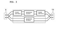
- the phase-shift amount y of the phase shifter 4 is set to be substantially (90°+n ⁇ 180°), and the phase-shift amount z of the phase shifter 5 is set to be substantially (90°+m ⁇ 180°), and in the modified example shown in FIG. 3, the phase-shift amount x of the phase shifter 3 is set to be substantially (90°+n ⁇ 180°), and the phase-shift amount y of the phase shifter 4 is set to be substantially (90°+m ⁇ 180°).
- the term “substantially” in this application means that a range of about ⁇ 30% is allowed
- phase shift unit is not particularly restricted, and various known phase shifters can be used.
- phase shifters may include delay lines, which are preferably formed of conductor strip lines, on a dielectric substrate. Delay lines formed of conductor strip lines have a simple structure and can be manufactured at low cost.
- the phase shifters may include capacitor devices and inductor devices connected in series with the capacitor devices.
- capacitor devices and the inductor devices small devices that can be used in a microwave or millimetric wave band are commercially available.
- the inductor devices and capacitor devices may be formed on a SAW substrate according to a thin-film microprocessing technique so as to form small phase shifters, thereby reducing the size of the overall bandpass filter unit of various preferred embodiments of the present invention.
- phase shift units of the present invention do not have to be formed of the above-described known phase shifters, and may be formed of wiring, a conductive pattern or bonding wire.
- the bandpass filter unit of preferred embodiments of the present invention includes first and second bandpass filters, which may increase the size of the overall bandpass filter unit.
- SAW filters small SAW filters
- SAW filter electrodes can be formed on a piezoelectric substrate according to an ultra-microprocessing technique. It is thus possible to provide a bandpass filter unit of preferred embodiments of the present invention without significantly increasing the overall size.
- SAW filters are used as the bandpass filters 1 and 2 .
- SAW filters resonator SAW filters, transversal SAW filters, or SAW filters including a combination of a plurality of one-terminal-pair SAW resonators defining a ladder or lattice circuit may be used.
- SAW filters including a combination of resonator SAW filters and one-terminal-pair SAW resonators are used as bandpass filters in cellular telephones.
- SAW filters may be used as the first and second bandpass filters 1 and 2 .
- first and second bandpass filters 1 and 2 are defined by SAW filters, they can be disposed on the same piezoelectric substrate, and also, phase shifters are defined by conductor strip lines. It is thus possible to further reduce the size of the bandpass filter unit of preferred embodiments of the present invention.
- first and second bandpass filters 1 and 2 are defined by SAW filters
- opposing electrodes are disposed on the same piezoelectric substrate on which the first and second bandpass filters 1 and 2 are disposed so as to define capacitor devices, which can be used as a portion of components forming the phase shifters. Accordingly, the size of the bandpass filter unit can also be reduced.
- the resonator SAW filter unit 500 shown in FIG. 12 was prepared as a comparative example. Details are as follows. A 40 ⁇ 5° rotating Y-cut and X-propagating LiTaO 3 substrate was preferably used as the piezoelectric substrate 501 .
- the electrode patterns on the piezoelectric substrate 501 were formed by Al thin film having a thickness of about 210 nm.
- the IDTs 514 and 516 were each formed of 12 pairs of opposing electrode fingers, and the line width and the pitch of the electrode fingers were about 0.68 ⁇ m and about 1.08 ⁇ m, respectively.
- the line width and the pitch of the electrode fingers were about 0.58 ⁇ m and about 0.97 ⁇ m, respectively.
- the IDT 515 was formed of 18.5 pairs of opposing electrode fingers, and the line width and the pitch of the electrode fingers were about 0.68 ⁇ m and about 1.08 ⁇ m, respectively.
- the line width and the pitch of the electrode fingers were about 0.58 ⁇ m and about 0.97 ⁇ m, respectively.
- grating reflectors each having 150 electrode fingers, both ends being short-circuited, were used.
- the line width and the pitch of the electrode fingers were about 0.62 ⁇ m and about 1.09 ⁇ m, respectively.
- the center-to-center distance of the electrode fingers between the reflector 513 and the IDT 514 was about 1.09 ⁇ m; the center-to-center distance between the IDT 514 and the IDT 515 was about 0.97 ⁇ m; the center-to-center distance between the IDT 515 and the IDT 516 was about 0.97 ⁇ m; and the center-to-center distance between the IDT 516 and the reflector 517 was about 1.09 ⁇ m.
- the length by which the opposing electrode fingers face each other (hereinafter referred to as the “interdigital length”) of the IDTs 514 , 515 , and 516 was about 200 ⁇ m.
- FIGS. 13 through 16 The transmission characteristic and the impedance characteristics of the input and output terminals of the comparative example configured as described above are shown in FIGS. 13 through 16, and are also indicated by broken lines in FIGS. 6 through 9.
- a bandpass filter unit 200 used in this example shown in FIGS. 4 and 5 was formed as follows.
- first and second bandpass filters 1 and 2 were designed in a manner similar to the resonator SAW filter unit 500 of the above-described comparative example.
- a 40 ⁇ 5° rotating Y-cut and X-propagating LiTaO 3 substrate was used to form a piezoelectric substrate 50 , and electrodes were formed by Al thin film having a thickness of about 210 nm.
- the interdigital length of the IDTs was about 100 ⁇ m. The reason for this is as follows.
- the impedance of each of the first and second bandpass filters 1 and 2 is preferably about 100 ⁇ , which is twice higher than that of the resonator SAW filter unit 500 , so that the impedance of the overall bandpass filter unit 200 becomes about 50 ⁇ .
- the capacitor devices 21 through 24 were each formed by allowing a pair of interdigital electrodes to interdigitate with each other. That is, a pair of opposing electrodes were disposed on the piezoelectric substrate 50 so as to form each of the capacitor devices 21 through 24 .
- the width of each electrode finger of the capacitor devices 21 through 24 was about 1.11 ⁇ m
- the spacing between opposing electrode fingers was about 1.11 ⁇ m
- the interdigital length was about 20 ⁇ m
- the numbers of pairs of the electrode fingers of the capacitor devices 21 through 24 were 92, 87, 87, and 89.5, respectively.
- the coil device 25 By grounding one terminal of the coil device 25 and by electrically connecting the other terminal to the electrode pad 27 on the piezoelectric substrate 50 , the coil device 25 was connected in series with the capacitor devices 21 and 22 . By grounding one terminal of the coil device 26 and by electrically connecting the other terminal to the electrode pad 28 on the piezoelectric substrate 50 , the coil device 26 was connected in series with the capacitor devices 23 and 24 . The electrode pads 29 through 33 on the piezoelectric substrate 50 were connected to ground potentials. The electrode pad 34 was used as the input terminal, and the electrode pad 35 was used as the output terminal. According to the configuration described above, the circuit configuration shown in FIG. 4 was implemented so as to form the bandpass filter unit 200 having a pass band of 1805 MHz to 1885 MHz.
- the capacitor devices 21 through 24 each includes opposing electrodes formed by allowing a pair of comb-like electrodes to interdigitate with each other.
- the electrostatic capacitances of the capacitor devices 21 through 24 in the range of 1805 MHz to 1885 MHz are approximately 0.80 pF, 0.70 pF, 0.70 pF, and 0.78 pF, respectively.
- the capacitor devices 21 and 22 , and the coil device 25 define the 90° phase shifter 4 having an overall characteristic impedance of about 100 ⁇ in the range of 1805 MHz to 1885 MHz.
- the capacitor devices 23 and 24 , and the coil device 26 define the 90° phase shifter 5 having a characteristic impedance of about 100 ⁇ in the range of 1805 MHz to 1885 MHz.
- the first and second bandpass filters 1 and 2 are resonator SAW filters having an interdigital length of about 100 ⁇ m, which is one half the interdigital length, i.e., about 200 ⁇ m, of the resonator SAW filter unit 500 of the comparative example.
- the characteristic impedance of each of the bandpass filters 1 and 2 becomes about 100 ⁇ .
- the transmission characteristic with respect to the frequency and the reflection characteristic (input/output impedance characteristics standardized by the characteristic impedance) of each of the bandpass filters 1 and 2 are substantially the same as those of the resonator SAW filter unit 500 of the comparative example, except that the characteristic impedance is about 100 ⁇ .
- the first and second bandpass filters 1 and 2 have a characteristic impedance of about 100 ⁇ in a pass band of 1805 MHz to 1885 MHz.
- the first bandpass filter 1 and the 90° phase shifter 4 are cascade-connected to define the filter circuit 7 .
- the 90° phase shifter 5 and the second bandpass filter 2 are cascade-connected to define the filter circuit 8 .
- the above-described bandpass filter unit 200 is provided.
- the bandpass filter unit 200 of this example has a circuit configuration similar to that shown in FIG. 2.
- the characteristic impedance of the filter circuits 7 and 8 is about 100 ⁇ , the characteristic impedance of the bandpass filter unit 200 becomes about 50 ⁇ .
- FIG. 6 illustrates the transmission characteristic of the bandpass filter unit 200 of this example and that of the resonator SAW filter unit 500 of the comparative example.
- FIG. 7 illustrates the enlarged essential portion of the transmission characteristic shown in FIG. 6.
- the solid lines indicate the transmission characteristic of this example, and the broken lines indicate the transmission characteristic of the comparative example.
- FIGS. 8 and 9 are Smith charts illustrating the impedance characteristic of the input terminal and that of the output terminal in the pass band of 1805 MHz to 1885 MHz.
- the solid lines indicate the impedance characteristic of this example, and the broken lines indicate the impedance characteristic of the comparative examples.
- the bandpass filter unit 200 of this example exhibits a very good impedance matching characteristic.
- the configurations of the bandpass filters 1 and 2 used in the bandpass filter unit 200 are substantially the same as those of the resonator SAW filter unit 500 , except that the impedance is twice as high as that of the comparative example.
- an improvement in the impedance matching characteristic shown in FIGS. 8 and 9 is obtained by the configuration of preferred embodiments of the present invention, i.e., by a combination of the first and second bandpass filters 1 and 2 and the phase shifters.
- FIGS. 6 and 7 show that the signal transmission efficiency of the bandpass filter unit 200 in the pass band is higher that that of the resonator SAW filter unit 500 . This is probably because the signal loss is reduced due to a smaller amount of reflection of the pass-band signals at the input and output terminals. According to preferred embodiments of the present invention, therefore, not only the impedance matching at the input and output terminals is improved, but also, the loss is reduced.
- the first and second bandpass filters 1 and 2 preferably have the same bandpass filter. However, they do not have to be the same.
- the characteristics of the bandpass filters 1 and 2 outside the pass band may be completely different as long as the characteristics in the pass band are substantially the same. If the difference in the transmission characteristic in the pass band between the bandpass filters 1 and 2 is not considerably large, the advantages of the present invention can still be obtained. Accordingly, it is only necessary that the pass-band transmission characteristics of the bandpass filters 1 and 2 substantially coincide with each other.
- bandpass filter unit As a bandpass filter unit related to the present invention, a configuration in which a plurality of bandpass filters having different pass bands are connected in parallel with each other is known. However, in such a bandpass filter unit, an increase in the pass band is targeted by differentiating the pass bands of the bandpass filters.
- bandpass filters having the same pass band are connected in parallel with each other, and phase shift unit are connected to at least one of the bandpass filters in order to prevent an adverse influence at input and output terminals rather than to increase the pass band. Accordingly, it should be noted that the bandpass filter unit of preferred embodiments of the present invention is totally different from a known bandpass filter formed by connecting two bandpass filters having different pass bands in parallel with each other.
- the phase-shift amount generated at the upstream or downstream portion of the circuit must be differentiated from that in a known bandpass filter unit formed by connecting a plurality of bandpass filters having different bands in parallel with each other.
- the length of the line from the input terminal pair 9 to the first bandpass filter 1 is substantially equal to that from the input terminal pair 9 to the second bandpass filter 2 .
- the length of the line from the first bandpass filter 1 to the output terminal pair 10 is preferably substantially equal to that from the second bandpass filter 2 to the output terminal pair 10 .
- FIG. 10 illustrates the circuit configuration of a bandpass filter unit 300 according to a second preferred embodiment of the present invention.
- the bandpass filter unit 300 includes a first bandpass filter 1 , a second bandpass filter 2 , a 45° phase shifter 3 , a ⁇ 45° phase shifter 4 , a ⁇ 45° phase shifter 5 , and a 45° phase shifter 6 .
- the characteristic impedance of the bandpass filter 1 is about 100 ⁇
- the characteristic impedance of the bandpass filter 2 is about 50 ⁇ . Except for the difference of the characteristic impedance, the bandpass filters 1 and 2 exhibit similar characteristics, such as the signal transmission efficiency with respect to the frequency and the reflection characteristic (input/output impedance characteristics standardized by the characteristic impedance).
- the characteristic impedances of the bandpass filters 1 and 2 can be easily differentiated as described above by setting the interdigital length of the bandpass filter 2 to be twice as long as that of the bandpass filter 1 .
- phase shifters 3 through 6 are connected in a manner similar to those of the bandpass filter unit 100 shown in FIG. 1.
- the characteristic impedances of the 45° phase shifter 3 and the ⁇ 45° phase shifter 4 are about 100 ⁇ .
- the characteristic impedances of the terminal of the ⁇ 45° phase shifter 5 connected to the bandpass filter 2 is about 50 ⁇ , and the characteristic impedance of the other terminal is about 100 ⁇ .
- the characteristic impedance of the terminal of the 45° phase shifter 6 connected to the bandpass filter 2 is about 50 ⁇ , and the characteristic impedance of the other terminal is about 100 ⁇ .
- the overall impedance of the bandpass filter unit 300 is about 50 ⁇ . Accordingly, in the second preferred embodiment, the pass-band matching characteristic of the input/output impedances can also be improved.
- the characteristic impedance of the bandpass filter 1 and that of the bandpass filter 2 are different, which apparently makes the pass-band characteristics of the bandpass filters 1 and 2 different.
- the transmission characteristic (frequency characteristic of the signal transmission efficiency) and the reflection characteristic (frequency characteristic of input/output impedances standardized by the characteristic impedance) are almost the same in the pass band. Accordingly, by providing the impedance conversion characteristic (transform characteristic) for the ⁇ 45° phase shifter 5 and the 45° phase shifter 6 in the bandpass filter unit 300 , the reflected waves occurring in the filter circuits 7 and 8 cancel each other out. It is thus possible to provide a bandpass filter unit having an improved pass-band matching characteristic of input/output impedances, as in the first preferred embodiment.
- the present invention encompasses such bandpass filters 1 and 2 as long as the pass-band characteristics standardized by the characteristic impedance are substantially the same.
- FIG. 11 is a circuit diagram illustrating a bandpass filter unit 600 according to a modified example of preferred embodiments of the present invention.
- the two bandpass filter units of the first preferred embodiment are connected in parallel with each other. That is, the bandpass filter unit 100 formed similar to the first preferred embodiment and a bandpass filter unit 100 A formed substantially similar to the first preferred embodiment are connected in parallel with each other.
- the pass band of the bandpass filter unit 100 is different from that of the bandpass filter unit 100 A. That is, the pass band of bandpass filters 1 A and 2 A used in the bandpass filter unit 100 A are different from the bandpass filters 1 and 2 of the bandpass filter unit 100 .
- the bandpass filter units 100 and 100 A having different pass bands are connected in parallel with each other so as to increase the pass band by a combination of the pass bands of the two filter units 100 and 100 A. Additionally, in each of the bandpass filter units 100 and 100 A, the pass-band impedance matching characteristic at the input/output terminals is improved according to preferred embodiments of the present invention.
Landscapes
- Physics & Mathematics (AREA)
- Acoustics & Sound (AREA)
- Surface Acoustic Wave Elements And Circuit Networks Thereof (AREA)
- Waveguide Switches, Polarizers, And Phase Shifters (AREA)
- Transceivers (AREA)
Abstract
Description
- 1. Field of the Invention
- The present invention relates to bandpass filter units and communication apparatuses, and more particularly, to a bandpass filter unit that is configured to suppress reflected waves at input and output terminals.
- 2. Description of the Related Art
- Bandpass filters have been used in transmission circuits or signal processing circuits in high frequency bands, such as microwave and millimetric wave bands. This type of bandpass filter includes, for example, surface acoustic wave (SAW) filters, dielectric filters, waveguide filters, microstrip line filters, and filters including lumped constant components having reactance (capacitors, chip inductors, air-core coils, etc.).
- FIG. 12 is a schematic plan view illustrating a resonator
SAW filter unit 500 as an example of known bandpass filters. In the resonatorSAW filter unit 500, aresonator SAW filter 502 is provided on a piezoelectricmonocrystal substrate 501. Theresonator SAW filter 502 includes interdigital transducers (IDTs) 514, 515, and 516 arranged in a direction in which a SAW propagates, andreflectors IDTs - An
electrode pad 509 connected to a ground potential and anelectrode pad 512, which defines an output terminal, are connected to thecentral IDT 515 via connectingconductors electrode pad 511, which defines an input terminal, is connected to one comb-like electrode of the IDT 514 and one comb-like electrode of the IDT 516 via connectingconductors electrode pad 510 connected to a ground potential is connected to the other comb-like electrodes of theIDTs 514 and 516 via connectingconductors - As the resonator
SAW filter unit 500, a bandpass filter having a characteristic impedance of 50 Ω and a pass band of 1805 MHz to 1885 MHz is provided. Examples of the characteristics of this bandpass filter are shown in FIGS. 13 through 16. FIG. 13 illustrates a transmission characteristic; FIG. 14 illustrates the enlarged essential portion of the transmission characteristic shown in FIG. 13; FIG. 15 is a Smith chart illustrating an impedance characteristic of the input terminal of the resonatorSAW filter unit 500 in the pass-band frequencies; and FIG. 16 is a Smith chart illustrating an impedance characteristic of the output terminal in the pass-band frequencies. - The principle of the operation of the resonator
SAW filter unit 500 is described in, for example, “SAW Device Technique Handbook” (edited by the SAW Device Technique 150th Committee of the Japan Society for the Promotion of Science, and published by Ohm-sha, Ltd.). - In bandpass filters used in microwave or millimetric bands, perfect impedance matching is preferably provided at input and output terminals. That is, it is desirable that signals in the pass band do not reflect at input and output terminals. This is because loss may be caused in reflected signals in the pass band, and also, reflected waves may produce an adverse influence on electric circuits connected to the bandpass filters.
- The above-described problem is more specifically explained below in the context of a bandpass filter disposed between an antenna and an amplifier in a receiver of a cellular telephone.
- If impedance matching is not provided for pass-band signals at the input terminal of a bandpass filter, the portion of a pass-band signal received by the antenna is reflected at the input terminal of the bandpass filter, thereby causing loss in the received signal. In this case, to compensate for the loss in the received signal, the gain of the amplifier must be increased for ensuring necessary signal intensity, resulting in an increase in the power consumption of the cellular telephone.
- Also, loss in a portion of the received signal decreases the signal-to-noise (S/N) ratio. Even if the signal level is increased by the amplifier at the subsequent stage, the S/N ratio is not recovered, thereby impairing the reception performance of the cellular telephone.
- The portion of the received signal reflected at the input terminal of the bandpass filter is also reflected at the antenna terminal, and is returned to the bandpass filter. Accordingly, due to this multiple reflection, a received signal having a phase delay is superposed on the normal received signal in the bandpass filter. Thus, due to this multiple reflection, the level of the received signal is also decreased, and the reception performance of the cellular telephone is impaired.
- As described above, the reflection of signals at the input terminal of the bandpass filter causes various adverse influences. It is thus demanded that the impedance matching be provided in the pass band so as to suppress the reflection of signals to a minimal level at the input terminal of the bandpass filter.
- If the impedance matching is not provided in the pass band at the output terminal of the bandpass filter, multiple reflection occurs in the pass-band signals between the output terminal of the bandpass filter and the input terminal of the amplifier. Accordingly, the operation of the amplifier, which is designed to provide the gain for the pass-band signals, becomes unstable, and in the worst case, abnormal oscillation occurs. If the level of the impedance mismatching at the output terminal of the bandpass filter is not considerably high, abnormal oscillation does not occur. In this case, however, the multiple reflections occurring between the bandpass filter and the amplifier due to the impedance mismatching inhibit, more or less, the normal operation of the bandpass filter. It is thus desirable that the impedance matching be also provided at the output terminal of the bandpass filter so as to suppress the reflection of signals.
- Generally, not only in this type of bandpass filter, but also in bandpass filters used in a microwave or millimetric wave band, it is desirable that the perfect impedance matching be provided at input and output terminals in the entire frequency range of the pass band so as to suppress reflection of pass-band signals at the input and output terminals.
- In reality, however, it is practically impossible to provide perfect impedance matching for the input and output terminals in the entire frequency range of the pass band because the input/output impedances of the bandpass filters have frequency characteristic. It is thus important that almost perfect impedance matching be provided in the entire frequency range of the pass band.
- The impedance characteristics at the input and output terminals of the known resonator
SAW filter unit 500 indicate, as shown in FIGS. 15 and 16, that the perfect impedance matching is not provided although the impedance is positioned close to the perfect matching point, which is the center of the Smith chart. That is, the impedance characteristic moves around the perfect matching point while exhibiting frequency characteristic. Accordingly, the reflection of the signals occurs at the input and output terminals in accordance with the distance of the input/output impedances to the perfect matching point. - In order to overcome the problems described above, preferred embodiments of the present invention provide a bandpass filter unit having an improved impedance matching characteristic in the entire frequency range of a pass band.
- According to a first preferred embodiment of the present invention, a bandpass filter unit includes a first filter, a second filter having a characteristic with respect to the frequency at least in a frequency band for use that is substantially the same as the characteristic of the first filter, the second filter being connected in parallel with the first filter, a first phase shift unit for shifting the phase by x degrees being cascade-connected to the input terminal of the first filter at a stage after parallel connecting points of the input terminals of the first filter and the second filter, a second phase shift unit for shifting the phase by y degrees being cascade-connected to the output terminal of the first filter at a stage before parallel connecting points of the output terminals of the first filter and the second filter, a third phase shift unit for shifting the phase by z degrees being cascade-connected to the input terminal of the second filter at a stage after the parallel connecting points of the input terminals of the first filter and the second filter, and a fourth phase shift unit for shifting the phase by w degrees being cascade-connected to the output terminal of the second filter at a stage before the parallel connecting points of the output terminals of the first filter and the second filter. The variables x, y, z, and w substantially satisfy the conditions expressed by equations (1) through (3):
- 2x−2z=180+n×360 (n is a certain integer); (1)
- 2y−2w=180+m×360 (m is a certain integer); (2)
- and
- x+y=z+w+l×360 (l is a certain integer). (3)
- According to a second preferred embodiment of the present invention, a bandpass filter unit includes a first filter, a second filter having a characteristic with respect to the frequency at least in a frequency band for use that is substantially the same as the characteristic of the first filter, the second filter being connected in parallel with the first filter, a phase shift unit for shifting the phase by substantially (90+n×180) degrees (n is a certain integer) being cascade-connected to the output terminal of the first filter at a stage before parallel connecting points of the output terminals of the first filter and the second filter, and a phase shift unit for shifting the phase by substantially (90+m×180) degrees (m is a certain integer, which is an odd number when n is an odd number or is an even number when n is an even number) being cascade-connected to the input terminal of the second filter at a stage after parallel connecting points of the input terminals of the first filter and the second filter.
- According to a third preferred embodiment of the present invention, a bandpass filter unit includes a first filter, a second filter having a characteristic with respect to the frequency at least in a frequency band for use that is substantially the same as the characteristic of the first filter, the second filter being connected in parallel with the first filter, a phase shift unit for shifting the phase by substantially (90+n×180) degrees (n is a certain integer) being cascade-connected to the input terminal of the first filter at a stage after parallel connecting points of the input terminals of the first filter and the second filter, and a phase shift unit for shifting the phase by substantially (90+m×180) degrees (m is a certain integer, which is an odd number when n is an odd number or is an even number when n is an even number) being cascade-connected to the output terminal of the first filter at a stage before parallel connecting points of the output terminals of the first filter and the second filter.
- With the above-described configuration, the reflected waves occurring in the first filter and the second filter cancel each other out, thereby preventing the occurrence of reflected waves at the input/output terminals. Accordingly, the reflection of pass-band signals at the input/output terminals is greatly reduced. It is thus possible to provide a bandpass filter unit providing excellent impedance matching at the input terminal. Additionally, since the reflection of pass-band signals can be reduced, the transmission efficiency of the pass-band signals is greatly improved.
- In preferred embodiments of the present invention, the above-described phase shift unit may preferably include known phase shift devices, for example, wiring forming the bandpass filter unit, as long as they are configured to shift the phase.
- According to a specific preferred embodiment of the present invention, at least one of the phase shift unit may be a delay line. The delay line can be easily formed on a circuit substrate or a piezoelectric substrate of the bandpass filter unit. With this arrangement, the phase shift unit can be easily formed.
- According to another specific preferred embodiment of the present invention, at least one of the phase shift units may include a capacitor device and an inductor device. In this case, by selecting the characteristics of the capacitor device and the inductor device, an optimal phase shift unit can be easily provided.
- The first filter and the second filter may include various types of bandpass filters, such as SAW filters, dielectric filters, and piezoelectric filters.
- According to still another specific preferred embodiment of the present invention, the first filter and the second filter may be SAW filters provided with a piezoelectric substrate, and the delay line may be defined by a conductor strip line disposed on the piezoelectric substrate. In this case, the delay line can be easily formed simply by forming a conductor strip line on the piezoelectric substrate forming the SAW filter. Also, the delay line can be formed integrally with the SAW filter, thereby reducing the size of the bandpass filter unit.
- According to a further specific preferred embodiment of the present invention, the first filter and the second filter may be SAW filters provided with a piezoelectric substrate, and at least one of the phase shift unit may be defined by a capacitor device and an inductor device, the capacitor device including an opposing electrode mounted on the piezoelectric substrate. In this case, the capacitor device can be easily formed by disposing an opposing electrode on the piezoelectric substrate of the SAW filter. Thus, the capacitor device can be easily formed without increasing the size of the bandpass filter unit.
- A communication apparatus of another preferred embodiment of the present invention includes the bandpass filter unit configured in accordance with the above-described preferred embodiments of the present invention as a bandpass filter.
- Other features, elements, characteristics and advantages of the present invention will become more apparent from the following detailed description of preferred embodiments with reference to the attached drawings.
- FIG. 1 illustrates the circuit configuration of a bandpass filter unit according to a first preferred embodiment of the present invention;
- FIG. 2 is a circuit diagram illustrating a modified example of the bandpass filter unit shown in FIG. 1;
- FIG. 3 is a circuit diagram illustrating another modified example of the bandpass filter unit shown in FIG. 1;
- FIG. 4 is a circuit diagram illustrating a bandpass filter unit used in an example;
- FIG. 5 is a schematic plan view illustrating the specific structure of the bandpass filter unit shown in FIG. 4;
- FIG. 6 illustrates the transmission efficiency with respect to the frequency of the bandpass filter unit shown in FIG. 4 and that of the resonator SAW filter unit of a comparative example;
- FIG. 7 illustrates an enlarged essential portion of the transmission efficiency shown in FIG. 6;
- FIG. 8 is a Smith chart illustrating a pass-band impedance characteristic at the input terminal of the bandpass filter unit shown in FIG. 4 and that of the resonator SAW filter unit of the comparative example;
- FIG. 9 is a Smith chart illustrating a pass-band impedance characteristic at the output terminal of the bandpass filter unit shown in FIG. 4 and that of the resonator SAW filter unit of the comparative example;
- FIG. 10 is a circuit diagram illustrating a bandpass filter unit according to a second preferred embodiment of the present invention;
- FIG. 11 is a circuit diagram illustrating still another modified example of the present invention;
- FIG. 12 is a schematic plan view illustrating a known resonator SAW filter unit;
- FIG. 13 illustrates the transmission efficiency with respect to the frequency of the known resonator SAW filter unit shown in FIG. 12;
- FIG. 14 illustrates an enlarged essential portion of the transmission efficiency shown in FIG. 13;
- FIG. 15 illustrates a pass-band impedance characteristic at the input terminal of the known resonator SAW filter unit shown in FIG. 12; and
- FIG. 16 illustrates a pass-band impedance characteristic at the output terminal of the known resonator SAW filter unit shown in FIG. 12.
- The present invention is described in detail below with reference to the accompanying drawings through illustration of preferred embodiments thereof.
- FIG. 1 is a circuit diagram illustrating the schematic configuration of a
bandpass filter unit 100 according to a first preferred embodiment of the present invention. - In the
bandpass filter unit 100, afirst bandpass filter 1 and asecond bandpass filter 2 having substantially the same characteristics in the pass band are used. That is, the first andsecond bandpass filters input terminal pair 9 and anoutput terminal pair 10. - A
phase shifter 3, which defines a first phase shift unit, for shifting the phase of a signal by x° is cascade-connected between theinput terminal pair 9 and thefirst bandpass filter 1. Aphase shifter 4, which defines a second phase shift unit, for shifting the phase of a signal by y° is cascade-connected between thebandpass filter 1 and theoutput terminal pair 10. Similarly, aphase shifter 5, which defines a third phase shift unit, for shifting the phase of a signal by z° is cascade-connected between theinput terminal pair 9 and thesecond bandpass filter 2, and aphase shifter 6, which defines a fourth phase shift unit, for shifting the phase of a signal by w° is cascade-connected between thebandpass filter 2 and theoutput terminal pair 10. - In other words, a
filter circuit 7 defined by sequentially cascade-connecting thephase shifter 3, thefirst bandpass filter 1, and thephase shifter 4 is connected in parallel with afilter circuit 8 defined by sequentially cascade-connecting thephase shifter 5, thesecond bandpass filter 2, and thephase shifter 6. - By connecting the
filter circuits bandpass filter unit 100 is produced. It should be noted that theinput terminal pair 9 and theoutput terminal pair 10 are connected to the parallel connecting points of the above-described parallel connection. - In the first preferred embodiment, the following equations (1) through (3) substantially hold true for the relationships among the amounts x, y, z, and w by which the phase is shifted (hereinafter referred to as “phase-shift amounts x, y, z, and w” of the
phase shifters - 2x−2z=180°+n×360° (n is a certain integer) (1)
- 2y−2w=180°+m×360° (m is a certain integer) (2)
- x+y=z+w+i×360° (i is a certain integer) (3)
- The operation of the
bandpass filter unit 100 and the provision of the impedance matching at the input and output terminals are described below. - The reflection of pass-band signals occurring at the
input terminal pair 9 is first discussed. Reflected waves at theinput terminal pair 9 are synthesized from reflected waves occurring in thefilter circuit 7 and those in thefilter circuit 8. Without thephase shifters second bandpass filters filter circuit 7 would be substantially in phase with and substantially have the same amplitude as those in thefilter circuit 8 since the band characteristics of thefirst bandpass filter 1 are substantially equal to those of thesecond bandpass filter 2. - With the
phase shifters 3, however, the reflected waves occurring in thefilter circuit 7 pass through thephase shifter 3 twice when advancing toward thefirst bandpass filter 1 and when returning to theinput terminal pair 9 by being reflected at the input terminal of thefirst bandpass filter 1. Accordingly, in thefilter circuit 7 provided with thephase shifter 3, the phase of the reflected waves is delayed by 2x° compared to thefilter circuit 7 without thephase shifter 3. - Similarly, in the
filter circuit 8 provided with thephase shifter 5, the phase of the reflected waves occurring in thefilter circuit 8 is delayed by 2z° compared to thefilter circuit 8 without thephase shifter 5. - Accordingly, even though the reflected waves occurring in the
filter circuit 7 have substantially the same amplitude as those in thefilter circuit 8, a phase difference of 2(x−z)° is generated between the reflected waves of thefilter circuit 7 and those of thefilter circuit 8. - Accordingly, equation (1) signifies that the phase of the reflected waves occurring in the
filter circuit 7 is inverted from those in thefilter circuit 8. That is, the reflected waves occurring in thefilter circuit 7 and those in thefilter circuit 8 are substantially 180° out of phase with each other and have substantially the same amplitude. Accordingly, the reflected waves occurring in thefilter circuit 7 and those in thefilter circuit 8 cancel each other out, and thus, the occurrence of reflected waves at theinput terminal pair 9 can be suppressed and prevented. - The occurrence of reflected waves can be suppressed and prevented as long as the frequency of an input signal is within the pass band. In the
bandpass filter unit 100 of the first preferred embodiment, therefore, the occurrence of reflected waves at the input terminal can be suppressed over the entire frequency range of the pass band. It is thus possible to provide a bandpass filter that exhibits an excellent impedance matching characteristic at the input terminal. - Also at the output terminal, the reflected waves occurring in the
filter circuit 7 and those in thefilter circuit 8 cancel each other out. That is, the characteristics of thebandpass filter 1 and those of thebandpass filter 2 in the pass band are almost the same as each other, and the relationship between the phase-shift amount y of thephase shifter 4 and the phase-shift amount w of thephase shifter 6 substantially satisfies equation (2). Accordingly, the reflected waves occurring in thefilter circuit 7 and those in thefilter circuit 8 cancel each other out, and thus, the occurrence of reflected waves at theoutput terminal pair 10 can also be substantially prevented in the entire frequency range of the pass band. - As discussed above, in the
bandpass filter unit 100 of the first preferred embodiment, the reflection at the input terminal and the output terminal can be suppressed and prevented. It is thus possible to provide a bandpass filter unit that exhibits an excellent impedance matching characteristic at input and output terminals. - The pass-band transmission characteristics of the
bandpass filter unit 100 are as follows. - Traveling waves passing through the
bandpass filter unit 100 are synthesized from traveling waves passing through thefilter circuit 7 and those passing through thefilter circuit 8. Thephase shifters filter circuit 7. Thephase shifters filter circuit 8. The difference of the phase-shift amount between thefilter circuit 7 and thefilter circuit 8 is an integral multiple of 360° from equation (3). - That is, the phase of the traveling waves passing through the
filter circuit 7 and the phase of the traveling waves passing through thefilter circuit 8 are almost the same as those when thephase shifters 3 through 6 are not provided. - Without the
phase shifters 3 through 6, the traveling waves passing through thefilter circuit 7 are exactly the same as those passing through thefirst bandpass filter 1, and the traveling waves passing through thefilter circuit 8 are exactly the same as those passing through thesecond bandpass filter 2. Since the band characteristics of thefirst bandpass filter 1 and those of thesecond bandpass filter 2 are substantially the same, the traveling waves of the first andsecond bandpass filters - The phase relationship between the traveling waves passing through the
filter circuit 7 and those passing through thefilter circuit 8 is almost the same as that between thebandpass filter unit 100 provided with thephase shifters 3 through 6 and a bandpass filter unit without thephase shifters 3 through 6. Accordingly, with thephase shifters 3 through 6, the traveling waves passing through thefilter circuit 7 become almost in phase with those passing through thefilter circuit 8. - Accordingly, the traveling waves passing through the
filter circuit 7 and those passing through thefilter circuit 8 are efficiently superposed on each other while being substantially in phase so as to synthesize the traveling waves output from thebandpass filter unit 100. - Therefore, the signal transmission efficiency of the overall
bandpass filter unit 100 is substantially similar to that of each of the first andsecond bandpass filters - In practice, since the loss caused by reflection is considerably reduced, the transmission efficiency of the
bandpass filter unit 100 is slightly improved over that of the first andsecond bandpass filters - Even if the band characteristics of the first and
second bandpass filters second bandpass filters bandpass filter unit 100. If the terminal conditions at the output terminals of thefirst bandpass filter 1 and those of thesecond bandpass filter 2 are exactly the same, the reflection characteristics of the input terminals of both thefilters first bandpass filter 1 and those of thesecond bandpass filter 2 are exactly the same, the reflection characteristics of the output terminals of both thefilters first bandpass filter 1 and that in thesecond bandpass filter 2 become slightly different from each other, and the reflection characteristics accordingly become slightly different between the first andsecond bandpass filters - In the
bandpass filter unit 100, since the input and output terminals of thefirst bandpass filter 1 are not in the same state as those of thesecond bandpass filter 2, the reflection characteristics become slightly different between the first andsecond bandpass filters bandpass filters filter circuit 7 do not completely cancel out the reflected waves in thefilter circuit 8, thereby causing a small amount of reflected waves in the overallbandpass filter unit 100. - However, by using filters that cause considerably a small amount of reflection in the pass band as the first and
second bandpass filters filter circuit 7 almost cancel out the reflected waves in thefilter circuit 8. Thus, thebandpass filter unit 100 exhibits a much smaller amount of reflection in the pass band than the single use of the first orsecond bandpass filter - In the present invention, it is not essential that the conditions expressed by equations (1) through (3) be precisely satisfied.
- That is, the advantages of the present invention can be obtained as long as 2x−2z, 2y−2w, and x+y in equations (1), (2), and (3) are within a range of approximately ±30% of 180°+n×360°, 180°+m×360°, and z+w+i×360°, respectively.
- In equation (1), if y is substantially (90°+n×180°) (n is a certain integer), and z is substantially (90°+m×180°) (m is a certain integer, which should be an odd number if n is an odd number and should be an even number if n is an even number), equations (1) and (2) hold true even if x and w are set to be 0. That is, the
phase shifters phase shifter 4 to be substantially (90°+n×180°) and the phase-shift amount z of thephase shifter 5 to be substantially (90°+m×180°), advantages similar to those achieved by the first preferred embodiment can be obtained. - In equations (1) through (3), x may be set to be substantially (90°+n×180°) and y may be set to be substantially (90°+m×180°) (m is a certain integer, which should be an odd number if n is an odd number and should be an even number if n is an even number), and z and w may be set to be 0. In this case, only the
phase shifters second bandpass filter 2. - In the modified examples shown in FIGS. 2 and 3, only two phase shifters are used, and thus, the circuit can be simplified compared to the
bandpass filter unit 100 shown in FIG. 1. - In the modified example shown in FIG. 2, the phase-shift amount y of the
phase shifter 4 is set to be substantially (90°+n×180°), and the phase-shift amount z of thephase shifter 5 is set to be substantially (90°+m×180°), and in the modified example shown in FIG. 3, the phase-shift amount x of thephase shifter 3 is set to be substantially (90°+n×180°), and the phase-shift amount y of thephase shifter 4 is set to be substantially (90°+m×180°). The term “substantially” in this application means that a range of about ±30% is allowed - In the present invention, the specific configuration of the phase shift unit is not particularly restricted, and various known phase shifters can be used. For example, phase shifters may include delay lines, which are preferably formed of conductor strip lines, on a dielectric substrate. Delay lines formed of conductor strip lines have a simple structure and can be manufactured at low cost.
- The phase shifters may include capacitor devices and inductor devices connected in series with the capacitor devices. As the capacitor devices and the inductor devices, small devices that can be used in a microwave or millimetric wave band are commercially available. The inductor devices and capacitor devices may be formed on a SAW substrate according to a thin-film microprocessing technique so as to form small phase shifters, thereby reducing the size of the overall bandpass filter unit of various preferred embodiments of the present invention.
- The phase shift units of the present invention do not have to be formed of the above-described known phase shifters, and may be formed of wiring, a conductive pattern or bonding wire.
- The bandpass filter unit of preferred embodiments of the present invention includes first and second bandpass filters, which may increase the size of the overall bandpass filter unit. However, by using small SAW filters as the first and second bandpass filters, SAW filter electrodes can be formed on a piezoelectric substrate according to an ultra-microprocessing technique. It is thus possible to provide a bandpass filter unit of preferred embodiments of the present invention without significantly increasing the overall size.
- Preferably, therefore, SAW filters are used as the
bandpass filters - Nowadays, SAW filters including a combination of resonator SAW filters and one-terminal-pair SAW resonators are used as bandpass filters in cellular telephones. Such SAW filters may be used as the first and
second bandpass filters - When the first and
second bandpass filters - When the first and
second bandpass filters second bandpass filters - A specific example of preferred embodiments of the present invention is as follows.
- In the following example, the resonator
SAW filter unit 500 shown in FIG. 12 was prepared as a comparative example. Details are as follows. A 40±5° rotating Y-cut and X-propagating LiTaO3 substrate was preferably used as thepiezoelectric substrate 501. The electrode patterns on thepiezoelectric substrate 501 were formed by Al thin film having a thickness of about 210 nm. TheIDTs 514 and 516 were each formed of 12 pairs of opposing electrode fingers, and the line width and the pitch of the electrode fingers were about 0.68 μm and about 1.08 μm, respectively. However, concerning a pair of electrode fingers of each of theIDTs 514 and 516 positioned adjacent to theIDT 515, the line width and the pitch of the electrode fingers were about 0.58 μm and about 0.97 μm, respectively. TheIDT 515 was formed of 18.5 pairs of opposing electrode fingers, and the line width and the pitch of the electrode fingers were about 0.68 μm and about 1.08 μm, respectively. However, for a pair of the outermost electrode fingers of theIDT 515, the line width and the pitch of the electrode fingers were about 0.58 μm and about 0.97 μm, respectively. - As the
reflectors - The center-to-center distance of the electrode fingers between the
reflector 513 and theIDT 514 was about 1.09 μm; the center-to-center distance between theIDT 514 and theIDT 515 was about 0.97 μm; the center-to-center distance between theIDT 515 and the IDT 516 was about 0.97 μm; and the center-to-center distance between the IDT 516 and thereflector 517 was about 1.09 μm. The length by which the opposing electrode fingers face each other (hereinafter referred to as the “interdigital length”) of theIDTs - The transmission characteristic and the impedance characteristics of the input and output terminals of the comparative example configured as described above are shown in FIGS. 13 through 16, and are also indicated by broken lines in FIGS. 6 through 9.
- In contrast to the comparative example, a
bandpass filter unit 200 used in this example shown in FIGS. 4 and 5 was formed as follows. In thebandpass filter unit 200, first andsecond bandpass filters SAW filter unit 500 of the above-described comparative example. As in the comparative example, a 40±5° rotating Y-cut and X-propagating LiTaO3 substrate was used to form apiezoelectric substrate 50, and electrodes were formed by Al thin film having a thickness of about 210 nm. In the first andsecond bandpass filters bandpass filters second bandpass filters SAW filter unit 500, so that the impedance of the overallbandpass filter unit 200 becomes about 50 Ω. - On the
piezoelectric substrate 50, not only the first andsecond bandpass filters capacitor devices 21 through 24, electrode pads 27 through 35, and connectingconductors 36 through 45 were disposed. - In this example, the
capacitor devices 21 through 24 were each formed by allowing a pair of interdigital electrodes to interdigitate with each other. That is, a pair of opposing electrodes were disposed on thepiezoelectric substrate 50 so as to form each of thecapacitor devices 21 through 24. The width of each electrode finger of thecapacitor devices 21 through 24 was about 1.11 μm, the spacing between opposing electrode fingers was about 1.11 μm, the interdigital length was about 20 μm, and the numbers of pairs of the electrode fingers of thecapacitor devices 21 through 24 were 92, 87, 87, and 89.5, respectively. - The above-described
piezoelectric substrate 50, a 10 nH chip inductor, which defines acoil device 25, and a 10 nH chip inductor, which defines acoil device 26, were mounted on a dielectric substrate (not shown). - By grounding one terminal of the
coil device 25 and by electrically connecting the other terminal to the electrode pad 27 on thepiezoelectric substrate 50, thecoil device 25 was connected in series with thecapacitor devices coil device 26 and by electrically connecting the other terminal to theelectrode pad 28 on thepiezoelectric substrate 50, thecoil device 26 was connected in series with thecapacitor devices electrode pads 29 through 33 on thepiezoelectric substrate 50 were connected to ground potentials. Theelectrode pad 34 was used as the input terminal, and theelectrode pad 35 was used as the output terminal. According to the configuration described above, the circuit configuration shown in FIG. 4 was implemented so as to form thebandpass filter unit 200 having a pass band of 1805 MHz to 1885 MHz. - In the above-described example, the
capacitor devices 21 through 24 each includes opposing electrodes formed by allowing a pair of comb-like electrodes to interdigitate with each other. The electrostatic capacitances of thecapacitor devices 21 through 24 in the range of 1805 MHz to 1885 MHz are approximately 0.80 pF, 0.70 pF, 0.70 pF, and 0.78 pF, respectively. Thecapacitor devices coil device 25 define the 90°phase shifter 4 having an overall characteristic impedance of about 100 Ω in the range of 1805 MHz to 1885 MHz. Thecapacitor devices coil device 26 define the 90°phase shifter 5 having a characteristic impedance of about 100 Ω in the range of 1805 MHz to 1885 MHz. - As described above, the first and
second bandpass filters SAW filter unit 500 of the comparative example. By reducing the interdigital length to one half, the characteristic impedance of each of thebandpass filters bandpass filters SAW filter unit 500 of the comparative example, except that the characteristic impedance is about 100 Ω. - That is, the first and
second bandpass filters - The
first bandpass filter 1 and the 90°phase shifter 4 are cascade-connected to define thefilter circuit 7. The 90°phase shifter 5 and thesecond bandpass filter 2 are cascade-connected to define thefilter circuit 8. By connecting thefilter circuits bandpass filter unit 200 is provided. - That is, the
bandpass filter unit 200 of this example has a circuit configuration similar to that shown in FIG. 2. - Since the characteristic impedance of the
filter circuits bandpass filter unit 200 becomes about 50 Ω. - FIG. 6 illustrates the transmission characteristic of the
bandpass filter unit 200 of this example and that of the resonatorSAW filter unit 500 of the comparative example. FIG. 7 illustrates the enlarged essential portion of the transmission characteristic shown in FIG. 6. In FIGS. 6 and 7, the solid lines indicate the transmission characteristic of this example, and the broken lines indicate the transmission characteristic of the comparative example. FIGS. 8 and 9 are Smith charts illustrating the impedance characteristic of the input terminal and that of the output terminal in the pass band of 1805 MHz to 1885 MHz. In FIGS. 8 and 9, the solid lines indicate the impedance characteristic of this example, and the broken lines indicate the impedance characteristic of the comparative examples. - As shown in FIGS. 8 and 9, in the
bandpass filter unit 200 of this example, the input/output impedances are closer to the perfect matching point, which is the center of the Smith charts, in the entire frequency range of the pass band, than the resonatorSAW filter unit 500 of the comparative example. Accordingly, thebandpass filter unit 200 of this example exhibits a very good impedance matching characteristic. - The configurations of the
bandpass filters bandpass filter unit 200 are substantially the same as those of the resonatorSAW filter unit 500, except that the impedance is twice as high as that of the comparative example. Thus, an improvement in the impedance matching characteristic shown in FIGS. 8 and 9 is obtained by the configuration of preferred embodiments of the present invention, i.e., by a combination of the first andsecond bandpass filters - FIGS. 6 and 7 show that the signal transmission efficiency of the
bandpass filter unit 200 in the pass band is higher that that of the resonatorSAW filter unit 500. This is probably because the signal loss is reduced due to a smaller amount of reflection of the pass-band signals at the input and output terminals. According to preferred embodiments of the present invention, therefore, not only the impedance matching at the input and output terminals is improved, but also, the loss is reduced. - In the aforementioned first preferred embodiment and the example thereof, the first and
second bandpass filters bandpass filters bandpass filters bandpass filters - As a bandpass filter unit related to the present invention, a configuration in which a plurality of bandpass filters having different pass bands are connected in parallel with each other is known. However, in such a bandpass filter unit, an increase in the pass band is targeted by differentiating the pass bands of the bandpass filters. In contrast, according to the bandpass filter unit of preferred embodiments of the present invention, bandpass filters having the same pass band are connected in parallel with each other, and phase shift unit are connected to at least one of the bandpass filters in order to prevent an adverse influence at input and output terminals rather than to increase the pass band. Accordingly, it should be noted that the bandpass filter unit of preferred embodiments of the present invention is totally different from a known bandpass filter formed by connecting two bandpass filters having different pass bands in parallel with each other.
- Additionally, in the bandpass filter unit of preferred embodiments of the present invention, the phase-shift amount generated at the upstream or downstream portion of the circuit must be differentiated from that in a known bandpass filter unit formed by connecting a plurality of bandpass filters having different bands in parallel with each other.
- Preferably, in the
bandpass filter unit 200, the length of the line from theinput terminal pair 9 to thefirst bandpass filter 1 is substantially equal to that from theinput terminal pair 9 to thesecond bandpass filter 2. Similarly, the length of the line from thefirst bandpass filter 1 to theoutput terminal pair 10 is preferably substantially equal to that from thesecond bandpass filter 2 to theoutput terminal pair 10. With this arrangement, the reflected waves from the twofilter circuits - FIG. 10 illustrates the circuit configuration of a
bandpass filter unit 300 according to a second preferred embodiment of the present invention. Thebandpass filter unit 300 includes afirst bandpass filter 1, asecond bandpass filter 2, a 45°phase shifter 3, a −45°phase shifter 4, a −45°phase shifter 5, and a 45°phase shifter 6. The characteristic impedance of thebandpass filter 1 is about 100 Ω, and the characteristic impedance of thebandpass filter 2 is about 50 Ω. Except for the difference of the characteristic impedance, thebandpass filters - By the use of SAW filters as the first and
second bandpass filters bandpass filters bandpass filter 2 to be twice as long as that of thebandpass filter 1. - The
phase shifters 3 through 6 are connected in a manner similar to those of thebandpass filter unit 100 shown in FIG. 1. - The characteristic impedances of the 45°
phase shifter 3 and the −45°phase shifter 4 are about 100 Ω. The characteristic impedances of the terminal of the −45°phase shifter 5 connected to thebandpass filter 2 is about 50 Ω, and the characteristic impedance of the other terminal is about 100 Ω. The characteristic impedance of the terminal of the 45°phase shifter 6 connected to thebandpass filter 2 is about 50 Ω, and the characteristic impedance of the other terminal is about 100 Ω. - With this configuration, the overall impedance of the
bandpass filter unit 300 is about 50 Ω. Accordingly, in the second preferred embodiment, the pass-band matching characteristic of the input/output impedances can also be improved. - More specifically, in the
bandpass filter unit 300, the characteristic impedance of thebandpass filter 1 and that of thebandpass filter 2 are different, which apparently makes the pass-band characteristics of thebandpass filters phase shifter 5 and the 45°phase shifter 6 in thebandpass filter unit 300, the reflected waves occurring in thefilter circuits - As discussed above, even if the characteristic impedance is different between the first and
second bandpass filters bandpass filters - Not only in the above-described preferred embodiment, generally, even if the pass-band characteristics of two bandpass filters are apparently different, they can be corrected by phase shifters provided with a correction function, resulting in the bandpass filters exhibiting the substantially the same pass-band characteristics. Accordingly, reflected waves occurring in two filter circuits can cancel each other out in the almost entire frequency range of the pass band, thereby obtaining the advantages of the present invention.
- FIG. 11 is a circuit diagram illustrating a
bandpass filter unit 600 according to a modified example of preferred embodiments of the present invention. In thebandpass filter unit 600, the two bandpass filter units of the first preferred embodiment are connected in parallel with each other. That is, thebandpass filter unit 100 formed similar to the first preferred embodiment and abandpass filter unit 100A formed substantially similar to the first preferred embodiment are connected in parallel with each other. The pass band of thebandpass filter unit 100 is different from that of thebandpass filter unit 100A. That is, the pass band ofbandpass filters bandpass filter unit 100A are different from thebandpass filters bandpass filter unit 100. - In the
bandpass filter unit 600, thebandpass filter units filter units bandpass filter units - As described above, by connecting a plurality of the bandpass filter units of preferred embodiments of the present invention having different pass bands in parallel with each other, the impedance matching is greatly improved, and also, the pass band is significantly increased.
- It should be understood that the foregoing description is only illustrative of the present invention. Various alternatives and modifications can be devised by those skilled in the art without departing from the present invention. Accordingly, the present invention is intended to embrace all such alternatives, modifications and variances which fall within the scope of the appended claims.
Claims (21)
Applications Claiming Priority (2)
| Application Number | Priority Date | Filing Date | Title |
|---|---|---|---|
| JP2002-114935 | 2002-04-17 | ||
| JP2002114935A JP3932962B2 (en) | 2002-04-17 | 2002-04-17 | Band pass filter and communication device |
Publications (2)
| Publication Number | Publication Date |
|---|---|
| US20030197578A1 true US20030197578A1 (en) | 2003-10-23 |
| US6914477B2 US6914477B2 (en) | 2005-07-05 |
Family
ID=19194000
Family Applications (1)
| Application Number | Title | Priority Date | Filing Date |
|---|---|---|---|
| US10/408,281 Expired - Lifetime US6914477B2 (en) | 2002-04-17 | 2003-04-07 | Bandpass filter unit and communication apparatus |
Country Status (3)
| Country | Link |
|---|---|
| US (1) | US6914477B2 (en) |
| JP (1) | JP3932962B2 (en) |
| GB (1) | GB2387726B (en) |
Cited By (5)
| Publication number | Priority date | Publication date | Assignee | Title |
|---|---|---|---|---|
| US20160301377A1 (en) * | 2015-04-08 | 2016-10-13 | The Board Of Trustees Of The University Of Illinois | Tubular resonant filter and method of making a tubular resonant filter |
| US20190207325A1 (en) * | 2016-08-09 | 2019-07-04 | Tongyu Communication Inc. | Filter feeding network and base station antenna |
| US20230093885A1 (en) * | 2021-09-24 | 2023-03-30 | RF360 Europe GmbH | Harmonic Reduction with Filtering |
| US12113511B2 (en) | 2022-03-16 | 2024-10-08 | Rf360 Singapore Pte. Ltd. | Bridge-type filters |
| US12231112B2 (en) | 2022-03-16 | 2025-02-18 | Rf360 Singapore Pte. Ltd. | Bridge-type filters |
Families Citing this family (18)
| Publication number | Priority date | Publication date | Assignee | Title |
|---|---|---|---|---|
| CN100536328C (en) * | 2002-10-25 | 2009-09-02 | 日立金属株式会社 | Balanced-unblanced type multi-band filer module |
| US6963257B2 (en) * | 2004-03-19 | 2005-11-08 | Nokia Corporation | Coupled BAW resonator based duplexers |
| JP5261258B2 (en) * | 2009-03-30 | 2013-08-14 | 京セラ株式会社 | Bandpass filter |
| JP5451737B2 (en) * | 2011-12-28 | 2014-03-26 | 太陽誘電株式会社 | Front-end module |
| JP5986803B2 (en) * | 2012-05-24 | 2016-09-06 | 太陽誘電株式会社 | Filter, duplexer and communication module |
| USD732367S1 (en) | 2013-05-31 | 2015-06-23 | Irwin Industrial Tool Company | Utility knife handle |
| USD738182S1 (en) * | 2013-05-31 | 2015-09-08 | Irwin Industrial Tool Company | Utility knife |
| JP6889423B2 (en) * | 2018-02-05 | 2021-06-18 | 株式会社村田製作所 | Filter device, high frequency front end circuit, and communication device |
| US12155371B2 (en) | 2021-03-29 | 2024-11-26 | Murata Manufacturing Co., Ltd. | Layout of xbars with multiple sub-resonators in series |
| US11916539B2 (en) | 2020-02-28 | 2024-02-27 | Murata Manufacturing Co., Ltd. | Split-ladder band N77 filter using transversely-excited film bulk acoustic resonators |
| US10917072B2 (en) | 2019-06-24 | 2021-02-09 | Resonant Inc. | Split ladder acoustic wave filters |
| US11329628B2 (en) | 2020-06-17 | 2022-05-10 | Resonant Inc. | Filter using lithium niobate and lithium tantalate transversely-excited film bulk acoustic resonators |
| US12155374B2 (en) * | 2021-04-02 | 2024-11-26 | Murata Manufacturing Co., Ltd. | Tiled transversely-excited film bulk acoustic resonator high power filters |
| US12113512B2 (en) | 2021-03-29 | 2024-10-08 | Murata Manufacturing Co., Ltd. | Layout of XBARs with multiple sub-resonators in parallel |
| JP7343992B2 (en) * | 2019-03-20 | 2023-09-13 | 太陽誘電株式会社 | Filters and multiplexers |
| US12255625B2 (en) | 2020-02-28 | 2025-03-18 | Murata Manufacturing Co., Ltd. | Filter using transversely-excited film bulk acoustic resonators with inductively coupled sub-resonators |
| WO2023190114A1 (en) * | 2022-03-30 | 2023-10-05 | 京セラ株式会社 | Composite filter and communication device |
| KR102664839B1 (en) * | 2022-08-02 | 2024-05-10 | 한국전력공사 | intelligent terminal block |
Citations (6)
| Publication number | Priority date | Publication date | Assignee | Title |
|---|---|---|---|---|
| US3737813A (en) * | 1971-03-22 | 1973-06-05 | Siemens Ag | Transmission separation filter network for electric oscillations |
| US5294898A (en) * | 1992-01-29 | 1994-03-15 | Motorola, Inc. | Wide bandwidth bandpass filter comprising parallel connected piezoelectric resonators |
| US5721518A (en) * | 1996-06-13 | 1998-02-24 | Xetron Corporation | Cancellation technique for bandpass filters using a narrowband network having optimally coupled and overcoupled filters |
| US5815052A (en) * | 1995-05-31 | 1998-09-29 | Murata Manufacturing Co., Ltd. | High-frequency composite components comprising first and second circuits connected in parallel for multi-frequency systems |
| US6147571A (en) * | 1996-07-31 | 2000-11-14 | Matsushita Electric Industrial Co., Ltd. | Dual-band multilayer bandpass filter |
| US20020130729A1 (en) * | 2001-03-14 | 2002-09-19 | Lawrence Larson | Circuit and method improving linearity, and reducing distortion, in microwave RF bandpass filters, especially superconducting filters |
Family Cites Families (10)
| Publication number | Priority date | Publication date | Assignee | Title |
|---|---|---|---|---|
| JPS52154621A (en) * | 1976-06-18 | 1977-12-22 | Matsushita Electric Ind Co Ltd | Tone control device |
| JPS62257212A (en) * | 1986-04-30 | 1987-11-09 | Toyo Commun Equip Co Ltd | Idt resonator filter |
| JPH02156716A (en) * | 1988-12-09 | 1990-06-15 | Hitachi Ltd | Surface acoustic wave device, its connection method, and communication device using it |
| JPH0812961B2 (en) * | 1989-05-02 | 1996-02-07 | 株式会社村田製作所 | Parallel multi-stage bandpass filter |
| JPH03297211A (en) * | 1990-04-16 | 1991-12-27 | Oki Electric Ind Co Ltd | Surface acoustic wave filter |
| JPH0434023U (en) * | 1990-07-18 | 1992-03-19 | ||
| JPH057125A (en) * | 1991-06-27 | 1993-01-14 | Hitachi Ltd | Surface wave filters, demultiplexers and mobile radios |
| JP3199817B2 (en) * | 1992-03-04 | 2001-08-20 | 株式会社日立製作所 | Internally matched surface acoustic wave filter |
| JPH08321738A (en) * | 1995-05-24 | 1996-12-03 | Matsushita Electric Ind Co Ltd | Dual frequency bandpass filter, dual frequency demultiplexer and dual frequency synthesizer |
| JPH09214283A (en) * | 1996-02-01 | 1997-08-15 | Toyo Commun Equip Co Ltd | Surface acoustic wave device |
-
2002
- 2002-04-17 JP JP2002114935A patent/JP3932962B2/en not_active Expired - Lifetime
-
2003
- 2003-04-07 US US10/408,281 patent/US6914477B2/en not_active Expired - Lifetime
- 2003-04-08 GB GB0308119A patent/GB2387726B/en not_active Expired - Lifetime
Patent Citations (6)
| Publication number | Priority date | Publication date | Assignee | Title |
|---|---|---|---|---|
| US3737813A (en) * | 1971-03-22 | 1973-06-05 | Siemens Ag | Transmission separation filter network for electric oscillations |
| US5294898A (en) * | 1992-01-29 | 1994-03-15 | Motorola, Inc. | Wide bandwidth bandpass filter comprising parallel connected piezoelectric resonators |
| US5815052A (en) * | 1995-05-31 | 1998-09-29 | Murata Manufacturing Co., Ltd. | High-frequency composite components comprising first and second circuits connected in parallel for multi-frequency systems |
| US5721518A (en) * | 1996-06-13 | 1998-02-24 | Xetron Corporation | Cancellation technique for bandpass filters using a narrowband network having optimally coupled and overcoupled filters |
| US6147571A (en) * | 1996-07-31 | 2000-11-14 | Matsushita Electric Industrial Co., Ltd. | Dual-band multilayer bandpass filter |
| US20020130729A1 (en) * | 2001-03-14 | 2002-09-19 | Lawrence Larson | Circuit and method improving linearity, and reducing distortion, in microwave RF bandpass filters, especially superconducting filters |
Cited By (9)
| Publication number | Priority date | Publication date | Assignee | Title |
|---|---|---|---|---|
| US20160301377A1 (en) * | 2015-04-08 | 2016-10-13 | The Board Of Trustees Of The University Of Illinois | Tubular resonant filter and method of making a tubular resonant filter |
| US10003317B2 (en) * | 2015-04-08 | 2018-06-19 | The Board Of Trustees Of The University Of Illinois | Tubular resonant filter and method of making a tubular resonant filter |
| US20190207325A1 (en) * | 2016-08-09 | 2019-07-04 | Tongyu Communication Inc. | Filter feeding network and base station antenna |
| US10886634B2 (en) * | 2016-08-09 | 2021-01-05 | Tongyu Communication Inc. | Filter feeding network and base station antenna |
| US20230093885A1 (en) * | 2021-09-24 | 2023-03-30 | RF360 Europe GmbH | Harmonic Reduction with Filtering |
| WO2023046415A3 (en) * | 2021-09-24 | 2023-05-04 | RF360 Europe GmbH | Filter with reduced harmonics |
| US12267063B2 (en) * | 2021-09-24 | 2025-04-01 | Rf360 Singapore Pte. Ltd. | Harmonic reduction with filtering |
| US12113511B2 (en) | 2022-03-16 | 2024-10-08 | Rf360 Singapore Pte. Ltd. | Bridge-type filters |
| US12231112B2 (en) | 2022-03-16 | 2025-02-18 | Rf360 Singapore Pte. Ltd. | Bridge-type filters |
Also Published As
| Publication number | Publication date |
|---|---|
| JP3932962B2 (en) | 2007-06-20 |
| GB2387726A (en) | 2003-10-22 |
| GB0308119D0 (en) | 2003-05-14 |
| JP2003309450A (en) | 2003-10-31 |
| US6914477B2 (en) | 2005-07-05 |
| GB2387726B (en) | 2004-04-07 |
Similar Documents
| Publication | Publication Date | Title |
|---|---|---|
| US6914477B2 (en) | Bandpass filter unit and communication apparatus | |
| US7078989B2 (en) | Multi-mode surface acoustic wave filter device and duplexer | |
| US6900577B2 (en) | Surface acoustic wave device and communication apparatus | |
| US6522219B2 (en) | Surface acoustic wave ladder filter with two series resonators having different apodization weighting | |
| US9019040B2 (en) | Elastic wave branching filter | |
| US7049908B2 (en) | Surface acoustic wave device and communication apparatus | |
| KR100280611B1 (en) | Surface acoustic wave device | |
| EP1263137B1 (en) | Surface acoustic wave filter, balanced type filter and communication device | |
| US11277116B2 (en) | Multiplexer | |
| US11165409B2 (en) | Acoustic wave device, filter, and composite filter device | |
| US8106725B2 (en) | Acoustic wave filter device | |
| JP3743341B2 (en) | Surface acoustic wave device | |
| US20230078097A1 (en) | Surface-acoustic-wave resonator and filter utilizing effective reflecting structure | |
| EP1251637B1 (en) | Surface acoustic wave apparatus and communication apparatus | |
| JP3310132B2 (en) | Surface acoustic wave device and antenna duplexer using the same | |
| US7760048B2 (en) | Elastic wave filter and communication device equipped with the elastic wave filter | |
| US12431866B2 (en) | Acoustic wave filter | |
| US7880561B2 (en) | Surface acoustic wave filter device and duplexer | |
| CN222464583U (en) | Filter circuit and radio frequency front end module | |
| CN116210155B (en) | Multiplexer | |
| US12574014B2 (en) | Longitudinally coupled resonator acoustic wave filter and acoustic wave filter | |
| US20240333261A1 (en) | Multiplexer | |
| US20250330150A1 (en) | Ladder filter | |
| JP6747387B2 (en) | High frequency module | |
| CN117394822A (en) | A surface acoustic wave duplexer and communication equipment |
Legal Events
| Date | Code | Title | Description |
|---|---|---|---|
| AS | Assignment |
Owner name: MURATA MANUFACTURING CO., LTD., JAPAN Free format text: ASSIGNMENT OF ASSIGNORS INTEREST;ASSIGNOR:SHIBAHARA, TERUHISA;REEL/FRAME:013955/0589 Effective date: 20030402 |
|
| STCF | Information on status: patent grant |
Free format text: PATENTED CASE |
|
| FPAY | Fee payment |
Year of fee payment: 4 |
|
| FEPP | Fee payment procedure |
Free format text: PAYOR NUMBER ASSIGNED (ORIGINAL EVENT CODE: ASPN); ENTITY STATUS OF PATENT OWNER: LARGE ENTITY |
|
| FPAY | Fee payment |
Year of fee payment: 8 |
|
| FEPP | Fee payment procedure |
Free format text: PAYER NUMBER DE-ASSIGNED (ORIGINAL EVENT CODE: RMPN); ENTITY STATUS OF PATENT OWNER: LARGE ENTITY Free format text: PAYOR NUMBER ASSIGNED (ORIGINAL EVENT CODE: ASPN); ENTITY STATUS OF PATENT OWNER: LARGE ENTITY |
|
| FPAY | Fee payment |
Year of fee payment: 12 |