WO2019035283A1 - エッチング方法およびエッチング加工装置 - Google Patents
エッチング方法およびエッチング加工装置 Download PDFInfo
- Publication number
- WO2019035283A1 WO2019035283A1 PCT/JP2018/025193 JP2018025193W WO2019035283A1 WO 2019035283 A1 WO2019035283 A1 WO 2019035283A1 JP 2018025193 W JP2018025193 W JP 2018025193W WO 2019035283 A1 WO2019035283 A1 WO 2019035283A1
- Authority
- WO
- WIPO (PCT)
- Prior art keywords
- etching
- value
- distribution function
- ion energy
- energy distribution
- Prior art date
- Legal status (The legal status is an assumption and is not a legal conclusion. Google has not performed a legal analysis and makes no representation as to the accuracy of the status listed.)
- Ceased
Links
Images




Classifications
-
- H—ELECTRICITY
- H01—ELECTRIC ELEMENTS
- H01J—ELECTRIC DISCHARGE TUBES OR DISCHARGE LAMPS
- H01J37/00—Discharge tubes with provision for introducing objects or material to be exposed to the discharge, e.g. for the purpose of examination or processing thereof
- H01J37/32—Gas-filled discharge tubes
- H01J37/32917—Plasma diagnostics
- H01J37/32926—Software, data control or modelling
-
- H—ELECTRICITY
- H01—ELECTRIC ELEMENTS
- H01J—ELECTRIC DISCHARGE TUBES OR DISCHARGE LAMPS
- H01J37/00—Discharge tubes with provision for introducing objects or material to be exposed to the discharge, e.g. for the purpose of examination or processing thereof
- H01J37/32—Gas-filled discharge tubes
- H01J37/32917—Plasma diagnostics
- H01J37/32935—Monitoring and controlling tubes by information coming from the object and/or discharge
- H01J37/32954—Electron temperature measurement
-
- H—ELECTRICITY
- H01—ELECTRIC ELEMENTS
- H01J—ELECTRIC DISCHARGE TUBES OR DISCHARGE LAMPS
- H01J37/00—Discharge tubes with provision for introducing objects or material to be exposed to the discharge, e.g. for the purpose of examination or processing thereof
- H01J37/32—Gas-filled discharge tubes
- H01J37/32917—Plasma diagnostics
- H01J37/32935—Monitoring and controlling tubes by information coming from the object and/or discharge
- H01J37/32972—Spectral analysis
-
- H—ELECTRICITY
- H01—ELECTRIC ELEMENTS
- H01J—ELECTRIC DISCHARGE TUBES OR DISCHARGE LAMPS
- H01J37/00—Discharge tubes with provision for introducing objects or material to be exposed to the discharge, e.g. for the purpose of examination or processing thereof
- H01J37/32—Gas-filled discharge tubes
- H01J37/32917—Plasma diagnostics
- H01J37/3299—Feedback systems
-
- H—ELECTRICITY
- H05—ELECTRIC TECHNIQUES NOT OTHERWISE PROVIDED FOR
- H05H—PLASMA TECHNIQUE; PRODUCTION OF ACCELERATED ELECTRICALLY-CHARGED PARTICLES OR OF NEUTRONS; PRODUCTION OR ACCELERATION OF NEUTRAL MOLECULAR OR ATOMIC BEAMS
- H05H1/00—Generating plasma; Handling plasma
- H05H1/24—Generating plasma
- H05H1/46—Generating plasma using applied electromagnetic fields, e.g. high frequency or microwave energy
-
- H—ELECTRICITY
- H10—SEMICONDUCTOR DEVICES; ELECTRIC SOLID-STATE DEVICES NOT OTHERWISE PROVIDED FOR
- H10P—GENERIC PROCESSES OR APPARATUS FOR THE MANUFACTURE OR TREATMENT OF DEVICES COVERED BY CLASS H10
- H10P50/00—Etching of wafers, substrates or parts of devices
- H10P50/20—Dry etching; Plasma etching; Reactive-ion etching
- H10P50/24—Dry etching; Plasma etching; Reactive-ion etching of semiconductor materials
- H10P50/242—Dry etching; Plasma etching; Reactive-ion etching of semiconductor materials of Group IV materials
-
- H—ELECTRICITY
- H10—SEMICONDUCTOR DEVICES; ELECTRIC SOLID-STATE DEVICES NOT OTHERWISE PROVIDED FOR
- H10P—GENERIC PROCESSES OR APPARATUS FOR THE MANUFACTURE OR TREATMENT OF DEVICES COVERED BY CLASS H10
- H10P50/00—Etching of wafers, substrates or parts of devices
- H10P50/20—Dry etching; Plasma etching; Reactive-ion etching
- H10P50/28—Dry etching; Plasma etching; Reactive-ion etching of insulating materials
- H10P50/282—Dry etching; Plasma etching; Reactive-ion etching of insulating materials of inorganic materials
- H10P50/283—Dry etching; Plasma etching; Reactive-ion etching of insulating materials of inorganic materials by chemical means
Definitions
- the present technology relates to an etching method and etching processing apparatus suitable for atomic layer etching (ALE), for example.
- ALE atomic layer etching
- atomic layer etching of a silicon (Si) wafer is performed as follows. First, a halogen-based gas such as chlorine (Cl) is adsorbed on the wafer surface. Then vacuum the excess gas and tap the surface with argon (Ar) ions. This removes one layer of Si on the wafer surface in the form of a reaction product (SiCl).
- a halogen-based gas such as chlorine (Cl) is adsorbed on the wafer surface.
- Ar argon
- etching depth represents the depth of the removed film
- damage represents the deterioration of the film due to the penetration of ions or the like.
- etching method In the etching method according to an embodiment of the present technology, at least power, pressure, and gas flow rate are input to the setting unit, and the etching process is performed in the chamber according to the values input to the setting unit.
- the ion energy distribution function is calculated using the measured value of.
- the ion energy distribution function is calculated during the etching process, for example, the maximum energy value of the ion energy distribution function is extracted.
- a setting unit to which at least a power, a pressure, and a gas flow rate are input, a chamber to which an etching process is performed according to a value input to the setting unit, and etching
- a processing unit that calculates an ion energy distribution function using measured values during processing.
- a processing unit that calculates the ion energy distribution function in the etching process is provided, so that, for example, the maximum energy value of the ion energy distribution function is extracted.
- the ion energy distribution function is calculated at the time of the etching process. Therefore, according to the maximum energy value of the extracted ion energy distribution function The processing conditions of etching can be adjusted. Therefore, it is possible to control the etching depth and the damage on the wafer with high accuracy.
- FIG. (A) to (D) are diagrams for sequentially explaining a process of atomic layer etching. It is a figure showing the relation between self bias voltage and ion energy. It is a block diagram showing composition of an important section of an etching processing device concerning a modification. It is a flowchart showing the operation
- Embodiment Etching apparatus having a processing unit that calculates an ion energy distribution function Modification Example of calculating ion energy distribution function using simulation
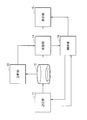
- FIG. 1 shows the configuration of the main part of an etching apparatus (etching apparatus 1) according to an embodiment of the present technology.
- the etching processing apparatus 1 is for performing, for example, atomic layer etching, and includes a setting unit 11, a chamber 12, an analysis unit 13, a processing unit 14, a display unit 15, and a control unit 16.
- a setting unit 11 a chamber 12, an analysis unit 13, a processing unit 14, a display unit 15, and a control unit 16.
- a control unit 16 In the chamber 12, opposing upper and lower electrodes are provided, and a wafer to be etched is disposed on the lower electrode. When a voltage is applied to the upper electrode and the lower electrode, the gas between them becomes plasma and the wafer surface is etched.
- the setting unit 11 is for setting processing conditions of etching performed in the chamber 12.
- a so-called process recipe is input to the setting unit 11.
- the setting unit 11 receives, for example, normal process recipes such as the power amount of each of the upper electrode and the lower electrode, the pressure in the chamber 12, the flow rate of the gas supplied into the chamber 12, the temperature in the chamber 12, and the processing time. Be done.
- the setting unit 11 is configured to receive a maximum energy value E SV of an ion energy function that enables atomic level etching.
- the maximum energy value E SV of the ion energy function input to the setting unit 11 is adjusted in accordance with the object to be etched, the state in the chamber 12, and the like.
- the maximum energy value E SV of the ion energy function is set to 20 eV or less.
- the absence of oxygen means not only the absence of oxygen due to gas introduction but also the release of oxygen from each component in the chamber 12.
- the maximum energy value E SV of the ion energy function is set to 20 eV or more.
- the maximum energy value E SV of the ion energy function is set to 40 eV or less.
- the etching gas contains fluorinated hydrocarbon (CF or CHF)
- the etching process is performed according to the conditions input to the setting unit 11.
- the etching target is, for example, silicon (Si) or silicon oxide (SiO 2 ).
- the chamber 12 is provided with a heater for controlling, for example, the temperature of the wall in the chamber 12 and the temperature of a mechanism (electrostatic chuck) for adsorbing the wafer to the stage.
- the chamber 12 is provided with a gas supply port and an exhaust port, and a halogen-based etching gas containing, for example, fluorine (F) or chlorine (Cl) is supplied.
- the gas supplied into the chamber 12 contains two or more types of noble gases.
- the noble gas may be included in the process recipe or may be added separately from the process recipe. When adding separately from the process recipe, for example, the noble gas is made to be 5% or less.
- the two or more types of noble gases are selected from, for example, helium (He), neon (Ne), argon (Ar), xenon (Xe) and krypton (Kr).
- the electron temperature distribution (EEDF: Electron Energy Distribution Function) of the plasma can be more accurately determined from the light emission intensity ratio of the two or more types of noble gases. It can be calculated.
- optical emission spectroscopy (OES) in the chamber 12 is performed.
- the resolution of emission spectral analysis is preferably 0.1 nm or less.
- the analysis result of the emission spectral analysis is used when the processing unit 14 calculates the ion energy distribution function.
- FIG. 2 shows an example of the result of emission spectral analysis in the analysis unit 13.
- the analysis unit 13 for example, the emission intensity of each of two or more different wavelengths of light and the emission intensity of each of two or more types of rare gases supplied to the chamber 12 are measured.
- the ion energy distribution function is calculated from the state in the chamber 12. Specifically, the power amounts of the upper electrode and the lower electrode, the pressure in the chamber 12, the flow rate of the gas supplied into the chamber 12, the measured value (measured value) of the temperature in the chamber 12, and the analysis value of the analysis unit 13 And the ion energy distribution function is calculated using, for example, Monte Carlo simulation.
- the processing unit 14 that calculates the ion energy distribution function is provided, it is possible to perform feedback according to the maximum energy value (energy value E MAX described later) of the ion energy distribution function. Although details will be described later, this makes it possible to control the etching depth and the damage on the wafer with high precision.
- the calculation of the ion energy distribution function ⁇ by Monte Carlo simulation in the processing unit 14 is performed, for example, according to the following equations (1) to (6) (for example, K. Denpoh et al., Jpn. J. Appl. Phys. 43 (2004) 5533 and D. Vender and RWBoswell, IEEE Trans. Plasma Sci. 18 (1990) 725).
- the peak-to-peak voltage Vpp in the chamber 12 is measured, and the RF amplitude V RF of the equations (1) and (2) is determined from the measured value of the peak-to-peak voltage Vpp using the following equation (7)
- You may A calibration curve (Vdc ⁇ ⁇ Vpp + ⁇ , where ⁇ and ⁇ are constants) of peak-to-peak voltage Vpp and self-bias voltage Vdc is prepared in advance, and using this calibration curve, peak-to-peak voltage Vpp
- the self bias voltage Vdc obtained from the measured value may be used in the equations (2) and (5).
- the self bias voltage Vdc in the chamber 12 may be measured, and the measured value of the self bias voltage Vdc may be used in the equations (2) and (5).
- the plasma potential Vpl of the equations (2) and (5), the electron temperature Te of the equations (4) and (6), and the electron density Ne of the equation (6) are obtained, for example, from the analysis results of emission spectroscopy in the analysis unit 13 It is calculated.
- the electron temperature Te can be calculated using the emission intensity ratio of light of two or more different wavelengths (see, for example, H. Akatsuka et al., Proc. Of 2015 International Symposium on Dry Process, P 95). .
- an electron temperature distribution may be used.
- the electron temperature distribution is calculated from the emission intensity ratio of two or more types of noble gases supplied to the chamber 12 by Maxwell distribution or Bi-Maxwell distribution.
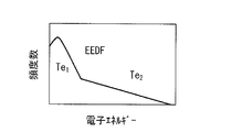
- FIG. 3A shows an example of the electron temperature distribution calculated by Maxwell distribution
- FIG. 3B shows an example of the electron temperature distribution calculated by Bi-Maxwell distribution.
- the electron temperature distribution calculated by such Maxwell distribution or Bi-Maxwell distribution is used for calculation of the ion energy distribution function and displayed on the display unit 15, for example.
- the display unit 15 is configured of, for example, a display.
- the electron density Ne can be calculated using the emission intensity ratio of light of two or more different wavelengths (for example, H. Akatsuka et al., Proc. Of 2015 International Symposium on Dry Process, P 95).
- the plasma potential Vpl can be determined using the following equation (8).
- the value of the coefficient k changes in the range of, for example, about 3 to 7 depending on the ion species. For example, when using argon (Ar) ions, the coefficient k is about 5, and when using hydrogen (H), the coefficient k is about 3.3.
- the thickness of these films is preferably measured by using a method such as ellipsometry.
- the energy loss caused by these films is taken into consideration in the processing unit 14.
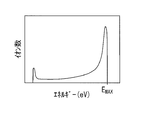
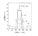
- FIG. 4 shows an example of the ion energy distribution function calculated by the processing unit 14.
- the horizontal axis represents energy
- the vertical axis represents the number of ions.
- Such an energy distribution function is displayed on the display unit 15 in real time.
- the processing unit 14 extracts the maximum energy value E MAX from the calculated ion energy distribution function, displays it on the display unit 15, and transmits information on the maximum energy value E MAX to the control unit 16.
- the maximum energy value E MAX often overlaps with the position of the peak as shown in FIG. 4, the position of the highest energy (for example, the right end of the horizontal axis in FIG. 4) even if the peak is not detected ) Should be extracted.
- the case where the peak is not detected is, for example, the case where the pressure is high.
- the processing unit 14 may calculate the entire area (integral value) of the ion energy distribution function and transmit this to the control unit 16 together with the maximum energy value E MAX .
- the electron density Ne may be predicted from the entire area of the ion energy distribution function.
- the display unit 15 may display the electron density Ne, the molecular weight mi, the RF amplitude VRF, and the like. Based on the result calculated by the processing unit 14, the etching depth and the damage depth of the object may be confirmed on the display unit 15.
- the display unit 15 is configured to display the distribution of the penetration depth of ions (damage), the projected range (peak depth of damage), and the deepest distance of the ions.
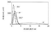
- FIG. 5A and 5B are image diagrams of the distribution of the penetration depth of ions displayed on the display unit 15.
- FIG. For example, by previously inputting the type of the etching object to the setting unit 11, it is possible to confirm the etching depth of the object on the display unit 15 in this manner.
- the control unit 16 compares the maximum energy value E MAX extracted by the processing unit 14 with the maximum energy value E SV input to the setting unit 11.
- the deviation between the energy value E MAX and the energy value E SV may be displayed on the display unit 15.
- the control unit 16 sends a signal to the setting unit 11 so that the maximum energy value E MAX calculated based on the state in the chamber 12 approaches the maximum energy value E SV input to the setting unit 11.
- a bias power (Bias Power) in which the energy value E MAX is within ⁇ 10% of the energy value E SV is calculated, and the power amount of the upper electrode and the lower electrode for realizing this bias power
- the amount of electric power is sent to the setting unit 11.
- the amount of power of either one of the upper electrode and the lower electrode may be changed, or both of the amounts of power may be changed.
- the energy value E MAX is within ⁇ 10% of the energy value E SV , each value of the setting unit 11 is maintained as it is.
- the control unit 16 calculates source power for realizing this, and sends it to the setting unit 11.
- the total area of the ion energy distribution function is proportional to the current density (mA / cm 2 ), the ion flux (ion number / cm 2 / s) of the ions irradiated onto the wafer, and the electron density Ne in the plasma. Therefore, instead of the entire area of the ion energy distribution function, current density (mA / cm 2 ), ion flux (ion number / cm 2 / s) and electron density Ne may be input.
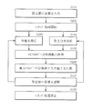
- FIG. 6 shows the flow of the etching process of such an etching apparatus 1.
- a general process recipe and the maximum energy value E SV of the ion energy function are input to the setting unit 11 (step S101).
- the etching process is started in the chamber 12 under the condition input to the setting unit 11 (step S102).
- the etching gas contains fluorinated hydrocarbon (CF or CHF)
- each value in the chamber 12 is measured (step S103). Specifically, peak-to-peak voltage Vpp or the like is measured.
- the emission spectroscopic analysis in the chamber 12 is performed in the analysis unit 13 (step S104).
- the measured values such as the peak-to-peak voltage Vpp and the analysis values of the analysis unit 13 are sent to the processing unit 14, and the processing unit 14 calculates an ion energy distribution function (step S105).
- the processing unit 14 extracts the maximum energy value E MAX from the ion energy distribution function.
- the ion energy distribution function and the maximum energy value E MAX are displayed on the display unit 15.
- the control unit 16 compares the energy value E SV input to the setting unit 11 with the energy value E MAX (step S106), and detects a deviation between them. This deviation is displayed on the display unit 15. The control unit 16 performs feedback to reduce this deviation. For example, the control unit 16 calculates a bias power (Bias Power) for bringing the energy value E MAX close to the energy value E SV , and sends this information to the setting unit 11.
- the setting unit 11 adjusts, for example, the amount of power of the upper electrode and the lower electrode based on the information from the control unit 16 (step S107).
- step S105 After adjusting each value of setting unit 11, measurement for detecting the state in chamber 12 is performed again (steps S103 and S104), calculation of ion energy distribution function (step S105), energy value E MAX and energy value E The comparison with the SV (step S106) and the feedback to the setting unit 11 (step S107) are repeated until the etching process is stopped (step S108).
- the etching processing apparatus 1 of the present embodiment since the ion energy distribution function is calculated in the processing unit 14 during the etching process in the chamber 12, the maximum energy value E MAX of the ion energy distribution function is extracted. Thus, the etching processing apparatus 1 can control the etching depth and the damage on the wafer with high accuracy. This will be described below.
- FIG. 7 shows each step of atomic layer etching.
- a halogen-based gas such as chlorine (Cl)
- Cl chlorine
- FIG. 7A the surface of the silicon wafer is struck with argon (Ar) ions
- FIG. 7B argon ions
- one atomic layer is removed in the form of a reaction product (SiCl)
- FIG. 7 (D) the removal of the silicon layer is one. There is a risk that the underlying silicon layer may be scraped off without stopping for a minute (FIG. 7 (D)).
- a method may be considered in which a self-bias voltage Vdc is determined from a peak-to-peak voltage Vpp using a calibration curve to control the self-bias voltage Vdc.
- ions have high energy above the voltage (center voltage) determined by the self-bias voltage Vdc. Therefore, even if the self bias voltage Vdc is controlled, the ion energy can not be controlled. That is, the etching depth and the damage on the wafer can not be controlled.
- the ion energy distribution function based on the state of the chamber 12 is calculated in the processing unit 14 and the maximum energy value E MAX is extracted.
- the etching processing conditions each value of the setting unit 11
- the etching processing conditions can be adjusted so that the energy value E MAX approaches the desired energy value E SV input to the setting unit 11. Therefore, atomic level etching can be performed without removing the underlying layer.
- the etching processing conditions are adjusted according to the maximum energy value E MAX of the extracted ion energy distribution function. can do. Therefore, it is possible to control the etching depth and the damage on the wafer with high accuracy.
- the etching state can be easily monitored.
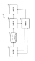
- FIG. 9 shows the configuration of the main parts of an etching apparatus (etching apparatus 1A) according to a modification of the above embodiment.
- the analysis unit analysis unit 13 in FIG. 1
- the processing unit (processing unit 14A) of the etching processing apparatus 1A performs more sophisticated calculation processing than the processing unit 14 of the etching processing apparatus 1. Except for this point, the etching processing apparatus 1A has the same configuration as the etching processing apparatus 1, and the operation and effect thereof are also the same.
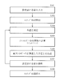
- FIG. 10 shows the operation of the etching apparatus 1A.
- the ion energy distribution function is calculated from the measured values in the chamber 12 (step S103) such as the peak-to-peak voltage Vpp and the calculated values of the simulation in the processing unit 14A. There is. That is, the parameters necessary for the calculation of the energy distribution function are calculated using the simulation in the processing unit 14A.
- the ion energy distribution function may be calculated by using simulation instead of emission spectral analysis.
- the present technology has been described above by the embodiment. However, the present technology is not limited to the above-described embodiment, and various modifications may be made.
- the components of the etching processing apparatus 1 and 1A illustrated in the above-described embodiment and the like are merely examples, and may further include other components.
- the etching method according to (3) wherein the measurement value includes an electron temperature Te or an electron temperature distribution EEDF, and an electron density Ne.
- the etching method according to (4) wherein the electron temperature Te or the electron temperature distribution EEDF and the electron density Ne are measured by performing an emission spectral analysis during the etching process.
- (6) Adding a noble gas into the chamber;
- the etching method according to (3), wherein the ion energy distribution function is calculated from the measured value and a calculated value obtained by simulation. (8) The calculated ion energy distribution function is displayed in real time.
- the etching process is atomic layer etching.
- the etching processing apparatus has a control unit, The value of the setting unit is adjusted by the control unit such that the calculated maximum energy value of the ion energy distribution function approaches the maximum energy value of the ion energy distribution function input in advance.
- Etching processing equipment Furthermore, it has an analysis part which performs emission spectrum analysis at the time of the etching process, The etching processing apparatus according to (11) or (12), wherein the analysis value analyzed by the analysis unit is input to the processing unit together with the measurement value. (14) Furthermore, it has a display part which displays the said calculated ion energy distribution function in real time, The etching processing apparatus as described in any one of said (11) thru
Landscapes
- Physics & Mathematics (AREA)
- Engineering & Computer Science (AREA)
- Plasma & Fusion (AREA)
- Chemical & Material Sciences (AREA)
- Analytical Chemistry (AREA)
- Spectroscopy & Molecular Physics (AREA)
- Electromagnetism (AREA)
- Drying Of Semiconductors (AREA)
- Plasma Technology (AREA)
Abstract
設定部に、少なくとも電力、圧力およびガス流量を入力し、前記設定部に入力された値に応じてチャンバ内でエッチング処理を行い、前記エッチング処理の際の測定値を用いてイオンエネルギー分布関数を計算するエッチング方法。
Description
本技術は、例えば原子層エッチング(ALE:Atomic Layer Etching)に好適なエッチング方法およびエッチング加工装置に関する。
半導体デバイスの微細化に伴い、例えば、原子層エッチング技術などの、より高精度な加工技術が必要とされている(例えば、特許文献1参照)。
例えばシリコン(Si)ウェハの原子層エッチングは、以下のようにして行う。まず、塩素(Cl)などのハロゲン系のガスを、ウェハ表面に吸着させる。次いで、余分なガスを真空引きした後、アルゴン(Ar)イオンで表面をたたく。これにより、反応生成物(SiCl)の形でウェハ表面の一層分のSiが除去される。
このような原子層エッチングなどのエッチング方法では、エッチング深さおよびウェハ上のダメージを高精度に制御することが望まれている。ここで、「エッチング深さ」は、除去された膜の深さを表し、「ダメージ」はイオン浸入等に起因した膜の変質を表す。
したがって、エッチング深さおよびウェハ上のダメージを高精度に制御することが可能なエッチング方法およびエッチング加工装置を提供することが望ましい。
本技術の一実施の形態に係るエッチング方法は、設定部に、少なくとも電力、圧力およびガス流量を入力し、設定部に入力された値に応じてチャンバ内でエッチング処理を行い、エッチング処理の際の測定値を用いてイオンエネルギー分布関数を計算するものである。
本技術の一実施の形態に係るエッチング方法では、エッチング処理の際にイオンエネルギー分布関数が計算されるので、例えばイオンエネルギー分布関数の最大エネルギー値が抽出される。
本技術の一実施の形態に係るエッチング加工装置は、少なくとも電力、圧力およびガス流量が入力される設定部と、設定部に入力された値に応じて、エッチング処理が施されるチャンバと、エッチング処理の際の測定値を用いてイオンエネルギー分布関数を計算する処理部とを備えたものである。
本技術の一実施の形態に係るエッチング加工装置では、エッチング処理の際のイオンエネルギー分布関数を計算する処理部が設けられているので、例えばイオンエネルギー分布関数の最大エネルギー値が抽出される。
本技術の一実施の形態に係るエッチング方法およびエッチング加工装置によれば、エッチング処理の際にイオンエネルギー分布関数を計算するようにしたので、抽出されたイオンエネルギー分布関数の最大エネルギー値に応じてエッチングの処理条件を調整することができる。よって、エッチング深さおよびウェハ上のダメージを高精度に制御することが可能となる。
尚、上記内容は本開示の一例である。本開示の効果は、上述したものに限らず、他の異なる効果であってもよいし、更に他の効果を含んでいてもよい。
以下、本技術の実施の形態について、図面を参照して詳細に説明する。なお、説明は以下の順序で行う。
1.実施の形態
イオンエネルギー分布関数を計算する処理部を有するエッチング加工装置
2.変形例
シミュレーションを用いてイオンエネルギー分布関数を計算する例
1.実施の形態
イオンエネルギー分布関数を計算する処理部を有するエッチング加工装置
2.変形例
シミュレーションを用いてイオンエネルギー分布関数を計算する例
〈実施の形態〉
[構成]
図1は、本技術の一実施の形態に係るエッチング加工装置(エッチング加工装置1)の要部の構成を表している。エッチング加工装置1は、例えば原子層エッチングを行うためのものであり、設定部11、チャンバ12、分析部13、処理部14、表示部15および制御部16を有している。チャンバ12内には、対向する上部電極および下部電極が設けられており、下部電極の上にエッチング対象となるウェハが配置される。上部電極および下部電極に電圧が印加されると、これらの間のガスがプラズマ化し、ウェハ表面がエッチングされるようになっている。
[構成]
図1は、本技術の一実施の形態に係るエッチング加工装置(エッチング加工装置1)の要部の構成を表している。エッチング加工装置1は、例えば原子層エッチングを行うためのものであり、設定部11、チャンバ12、分析部13、処理部14、表示部15および制御部16を有している。チャンバ12内には、対向する上部電極および下部電極が設けられており、下部電極の上にエッチング対象となるウェハが配置される。上部電極および下部電極に電圧が印加されると、これらの間のガスがプラズマ化し、ウェハ表面がエッチングされるようになっている。
設定部11は、チャンバ12内で行われるエッチングの処理条件を設定するためのものである。この設定部11に、いわゆるプロセスレシピが入力されるようになっている。設定部11には、例えば、上部電極および下部電極各々の電力量、チャンバ12内の圧力、チャンバ12内に供給されるガス流量、チャンバ12内の温度および処理時間などの通常のプロセスレシピが入力される。設定部11には、このような通常のプロセスレシピに加えて、原子レベルのエッチングが可能となるイオンエネルギー関数の最大エネルギー値ESVが入力されるようになっている。この設定部11に入力されるイオンエネルギー関数の最大エネルギー値ESVは、エッチング対象物およびチャンバ12内の状態等に応じて調整される。
例えば、エッチング対象物がシリコン(Si)であり、かつ、プラズマ中に酸素が存在しないとき、イオンエネルギー関数の最大エネルギー値ESVを、20eV以下に設定する。ここで酸素が存在しないとは、ガス導入による酸素が存在しないだけでなく、チャンバ12内の各部品からの酸素放出もないことをいう。エッチング対象物がシリコン(Si)であり、かつ、プラズマ中に酸素が存在するときは、イオンエネルギー関数の最大エネルギー値ESVを、20eV以上に設定する。
例えば、エッチング対象物が酸化シリコン(SiO2)であるとき、イオンエネルギー関数の最大エネルギー値ESVを、40eV以下に設定する。エッチングガスが、フッ素化炭化水素(CFまたはCHF)を含む場合には、CF膜またはCHF膜に起因したエネルギー損失を考慮してイオンエネルギー関数の最大エネルギー値ESVを設定することが好ましい。
チャンバ12では、設定部11に入力された条件に応じてエッチング処理が行われる。エッチング対象物は、例えばシリコン(Si)または酸化シリコン(SiO2)等である。チャンバ12には、例えばチャンバ12内の壁の温度およびウェハをステージに吸着する機構(静電チャック)の温度を制御するためのヒータが設けられている。このチャンバ12には、ガスの供給口および排気口が設けられ、例えば、フッ素(F)または塩素(Cl)等を含むハロゲン系のエッチングガスが供給されるようになっている。
チャンバ12内に供給されるガスには、2種類以上の希ガスが含まれていることが好ましい。この希ガスは、プロセスレシピに含まれていてもよく、プロセスレシピとは別に添加してもよい。プロセスレシピとは別に添加するときには、例えば希ガスが5%以下となるようにする。2種類以上の希ガスは、例えば、ヘリウム(He),ネオン(Ne),アルゴン(Ar),キセノン(Xe)およびクリプトン(Kr)から選択されている。チャンバ12内に2種類以上の希ガスを供給することにより、後述するように、2種類以上の希ガスの発光強度比から、より正確にプラズマの電子温度分布(EEDF:Electron Energy Distribution Function)を算出することができる。
分析部13では、チャンバ12内の発光分光分析(OES:Optical Emission Spectroscopy)がなされるようになっている。発光分光分析の分解能は、0.1nm以下であることが好ましい。この発光分光分析の解析結果は、処理部14でイオンエネルギー分布関数を計算する際に用いられる。
図2は、分析部13での発光分光分析の結果の一例を表している。分析部13では、例えば、2以上の互いに異なる波長の光各々の発光強度、およびチャンバ12に供給された2種類以上の希ガス各々の発光強度が測定される。
処理部14では、チャンバ12内の状態から、イオンエネルギー分布関数が計算される。具体的には、上部電極および下部電極各々の電力量、チャンバ12内の圧力、チャンバ12内に供給されるガス流量、チャンバ12内の温度の測定値(実測値)と分析部13の解析値とから、例えば、モンテカルロシミュレーションを用いて、イオンエネルギー分布関数が計算される。本実施の形態では、イオンエネルギー分布関数を計算する処理部14が設けられているので、イオンエネルギー分布関数の最大エネルギー値(後述のエネルギー値EMAX)に応じたフィードバックを行うことができる。詳細は後述するが、これにより、エッチング深さおよびウェハ上のダメージを高精度に制御することができる。
処理部14でのモンテカルロシミュレーションによるイオンエネルギー分布関数Δεの計算は、例えば以下の式(1)~(6)により行われる(例えば、K.Denpoh et al., Jpn. J. Appl. Phys. 43 (2004) 5533およびD.Vender and R.W.Boswell, IEEE Trans. Plasma Sci. 18 (1990) 725参照)。

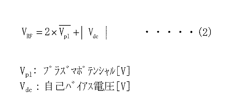
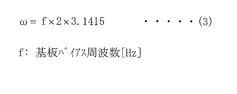
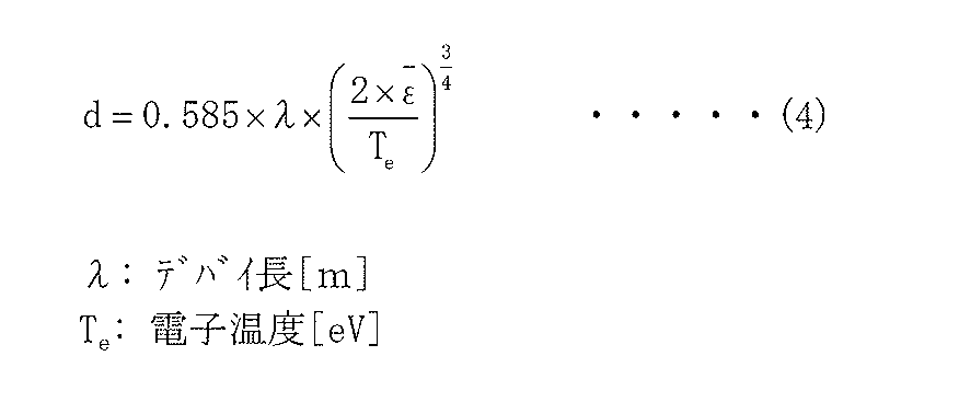


例えば、チャンバ12内のピークトゥピーク電圧Vppを測定し、このピークトゥピーク電圧Vppの測定値から以下の式(7)を用いて式(1),(2)のRF振幅VRFを求めるようにしてもよい。ピークトゥピーク電圧Vppと自己バイアス電圧Vdcとの校正曲線(Vdc=α×Vpp+β、αおよびβは定数)を事前に作成しておき、この校正曲線を用いて、ピークトゥピーク電圧Vppの測定値から求めた自己バイアス電圧Vdcを式(2),(5)に用いるようにしてもよい。
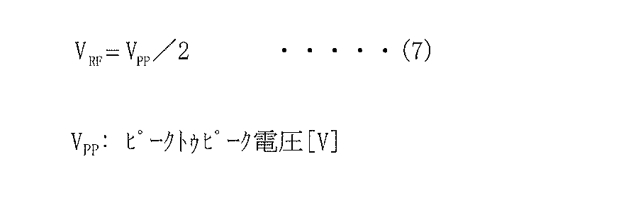
あるいは、チャンバ12内の自己バイアス電圧Vdcを測定し、この自己バイアス電圧Vdcの測定値を式(2),(5)に用いるようにしてもよい。上記と同様に、ピークトゥピーク電圧Vppと自己バイアス電圧Vdcとの校正曲線(Vdc=α×Vpp+β、αおよびβは定数)を事前に作成しておき、この校正曲線を用いて、自己バイアス電圧Vdcの測定値からピークトゥピーク電圧Vppを算出するようにしてもよい。この算出されたピークトゥピーク電圧Vppの値と式(7)とから式(1),(2)のRF振幅VRFが求められる。
式(2),(5)のプラズマポテンシャルVpl、式(4),(6)の電子温度Teおよび式(6)の電子密度Neは、例えば、分析部13での発光分光分析の解析結果から算出されるようになっている。
例えば、電子温度Teは、2以上の互いに異なる波長の光の発光強度比を用いて算出することができる(例えば、H.Akatsuka et al., Proc. Of 2015 International Symposium on Dry Process, P95参照)。
電子温度Teに代えて、電子温度分布を用いるようにしてもよい。電子温度分布は、チャンバ12に供給された2種類以上の希ガスの発光強度比から、Maxwell分布またはBi-Maxwell分布により算出される。
図3Aは、Maxwell分布により算出された電子温度分布の一例を表し,図3Bは、Bi-Maxwell分布により算出された電子温度分布の一例を表している。このようなMaxwell分布またはBi-Maxwell分布により算出された電子温度分布は、イオンエネルギー分布関数の計算に用いられるとともに、例えば、表示部15に表示される。表示部15は、例えばディスプレイにより構成されている。
電子密度Neは、2以上の互いに異なる波長の光の発光強度比を用いて算出することができる(例えば、H.Akatsuka et al., Proc. Of 2015 International Symposium on Dry Process, P95)。
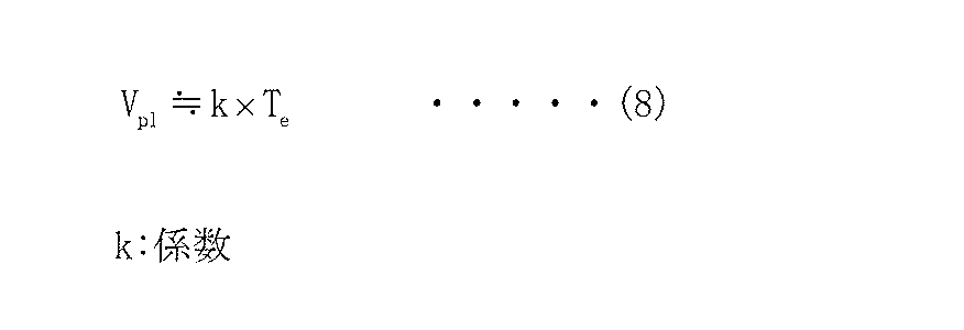
プラズマポテンシャルVplは、以下の式(8)を用いて求めることができる。式(8)中、係数kの値はイオン種により、例えば3~7程度の範囲で変化する。例えばアルゴン(Ar)イオンを用いるとき、係数kは約5であり、水素(H)を用いるとき係数kは約3.3である。
例えば、チャンバ12内にCF膜またはCHF膜が生成する場合には、これらの膜の厚みは、エリプソメトリ等の方法を用いることにより、測定することが好ましい。これらの膜に起因したエネルギー損失は、処理部14で考慮される。
図4は、処理部14で計算されたイオンエネルギー分布関数の一例を表している。この図では、横軸がエネルギー、縦軸がイオン数をそれぞれ表している。このようなエネルギー分布関数は、リアルタイムで表示部15に表示される。処理部14は、計算したイオンエネルギー分布関数から最大エネルギー値EMAXを抽出して、表示部15に表示するとともに、この最大エネルギー値EMAXに関する情報を制御部16に伝達する。最大エネルギー値EMAXは、図4に示したように、ピークの位置と重なることが多いが、ピークが検出されない場合であっても、最も高いエネルギーの位置(例えば、図4の横軸の右端)を抽出すればよい。ピークが検出されない場合とは、例えば、圧力が高い場合などである。
処理部14で、イオンエネルギー分布関数の全体の面積(積分値)を算出し、これを最大のエネルギー値EMAXとともに、制御部16に伝達するようにしてもよい。イオンエネルギー分布関数の全体の面積から電子密度Neを予測するようにしてもよい。
表示部15には、電子密度Ne、分子重さmiおよびRF振幅VRF等が表示されるようになっていてもよい。処理部14で計算された結果に基づき、表示部15で対象物のエッチング深さおよびダメージの深さが確認できるようになっていてもよい。例えば、表示部15に、イオン(ダメージ)の浸入深さの分布、投影飛程(ダメージのピーク深さ)およびイオンの最深距離が表示されるように構成されている。
図5A,図5Bは、表示部15に表示されるイオンの浸入深さの分布のイメージ図である。例えば、エッチング対象物の種類を予め設定部11に入力しておくことにより、このように対象物のエッチング深さを表示部15で確認することが可能となる。
制御部16では、処理部14で抽出された最大エネルギー値EMAXと、設定部11に入力された最大エネルギー値ESVとが比較される。エネルギー値EMAXとエネルギー値ESVとのずれを表示部15に表示するようにしてもよい。制御部16は、チャンバ12内の状態に基づいて計算された最大エネルギー値EMAXが、設定部11に入力された最大エネルギー値ESVに近づくように、設定部11に信号を送る。具体的には、エネルギー値EMAXが、エネルギー値ESVの±10%の範囲内となるバイアスパワー(Bias Power)が算出され、このバイアスパワーを実現するための上部電極の電力量および下部電極の電力量が、設定部11に送られるようになっている。設定部11では、上部電極および下部電極のどちらか一方の電力量が変更されてもよく、両方の電力量が変更されてもよい。エネルギー値EMAXが、エネルギー値ESVの±10%の範囲内にある場合には、設定部11の各値がそのまま維持される。
設定部11に予め、イオンエネルギー分布関数の全体の面積(積分値)を入力しておき、処理部14で算出されたイオンエネルギー分布関数の全体の面積が、この設定値に近づくようにしてもよい。制御部16では、これを実現するためのソースパワー(Source Power)が算出されて、設定部11に送られる。イオンエネルギー分布関数の全体の面積は、ウェハ上に照射されるイオンの電流密度(mA/cm2)、イオンフラックス(イオン個数/cm2/s)およびプラズマ中の電子密度Neに比例する。このため、イオンエネルギー分布関数の全体の面積に代えて、電流密度(mA/cm2)、イオンフラックス(イオン個数/cm2/s)および電子密度Neを入力するようにしてもよい。
[動作]
図6は、このようなエッチング加工装置1のエッチング処理の流れを表している。
図6は、このようなエッチング加工装置1のエッチング処理の流れを表している。
まず、設定部11に一般的なプロセスレシピおよびイオンエネルギー関数の最大エネルギー値ESVを入力する(ステップS101)。次に、この設定部11に入力された条件下、チャンバ12内でエッチング処理を開始する(ステップS102)。エッチングガスが、フッ素化炭化水素(CFまたはCHF)を含む場合には、ウェハ1枚を処理する毎に、少なくとも酸素を含むガスを用いて、チャンバ12内のプラズマクリーニングを行うことが好ましい。
エッチング処理開始後、チャンバ12内の各値を測定する(ステップS103)。具体的には、ピークトゥピーク電圧Vpp等を測定する。このステップS103ととともに、分析部13でチャンバ12内の発光分光分析を行う(ステップS104)。
ピークトゥピーク電圧Vpp等の測定値および分析部13の解析値は、処理部14へ送られ、処理部14でイオンエネルギー分布関数の計算が行われる(ステップS105)。処理部14では、このイオンエネルギー分布関数から最大エネルギー値EMAXを抽出する。イオンエネルギー分布関数および最大エネルギー値EMAXは、表示部15に表示される。
最大エネルギー値EMAXが抽出された後、制御部16は、設定部11に入力されたエネルギー値ESVと、エネルギー値EMAXとを比較し(ステップS106)、これらのずれを検出する。このずれは、表示部15に表示される。制御部16は、このずれを小さくするためのフィードバックを行う。例えば、制御部16は、エネルギー値EMAXをエネルギー値ESVに近づけるためのバイアスパワー(Bias Power)を算出し、この情報を設定部11に送る。設定部11では、制御部16からの情報に基づいて、例えば、上部電極および下部電極の電力量等が調整される(ステップS107)。設定部11の各値を調整後、再びチャンバ12内の状態を検出するための測定がなされ(ステップS103,S104)、イオンエネルギー分布関数の計算(ステップS105)、エネルギー値EMAXとエネルギー値ESVとの比較(ステップS106)および設定部11へのフィードバック(ステップS107)が、エッチング処理停止(ステップS108)時まで繰り返される。
[作用・効果]
本実施の形態のエッチング加工装置1では、チャンバ12でのエッチング処理の際に、処理部14でイオンエネルギー分布関数を計算するので、イオンエネルギー分布関数の最大エネルギー値EMAXが抽出される。これにより、エッチング加工装置1では、エッチング深さおよびウェハ上のダメージを高精度に制御することが可能となる。以下、これについて説明する。
本実施の形態のエッチング加工装置1では、チャンバ12でのエッチング処理の際に、処理部14でイオンエネルギー分布関数を計算するので、イオンエネルギー分布関数の最大エネルギー値EMAXが抽出される。これにより、エッチング加工装置1では、エッチング深さおよびウェハ上のダメージを高精度に制御することが可能となる。以下、これについて説明する。
図7は、原子層エッチングの各工程を表している。例えば、シリコン(Si)ウェハ表面に塩素(Cl)等のハロゲン系のガスを吸着させた後(図7(A))、アルゴン(Ar)イオンで、シリコンウェハ表面をたたく(図7(B)。これにより、反応生成物(SiCl)の形で、1層分の原子層が除去される(図7(C))。しかし、イオンエネルギーを調整しない場合には、シリコン層の除去が1層分で停止せずに、下地のシリコン層も削れてしまうおそれがある(図7(D))。
イオンエネルギーを計算せずに、他のパラメータのみで、エッチング深さおよびウェハ上のダメージを予測する方法も考え得る。例えば、ピークトゥピーク電圧Vppから校正曲線を用いて自己バイアス電圧Vdcを求め、この自己バイアス電圧Vdcを制御する方法が考えられる。
しかし、図8に示したように、自己バイアス電圧Vdcにより決まる電圧(中心の電圧)以上に、イオンは高いエネルギーを持つことになる。したがって、自己バイアス電圧Vdcを制御しても、イオンエネルギーを制御することはできない。即ち、エッチング深さおよびウェハ上のダメージを制御することできない。
これに対し、本実施の形態では、処理部14でチャンバ12の状態に基づくイオンエネルギー分布関数が計算され、最大エネルギー値EMAXが抽出される。これにより、このエネルギー値EMAXを、設定部11に入力した所望のエネルギー値ESVに近づけるように、エッチング処理条件(設定部11の各値)を調整することができる。したがって、下地層を削ることなく、原子レベルのエッチングを行うことができる。
以上説明したように、本実施の形態では、処理部14でイオンエネルギー分布関数を計算するようにしたので、抽出されたイオンエネルギー分布関数の最大エネルギー値EMAXに応じてエッチングの処理条件を調整することができる。よって、エッチング深さおよびウェハ上のダメージを高精度に制御することが可能となる。
また、計算されたイオンエネルギー分布関数は、表示部15にリアルタイムで表示されるので、エッチング状況を容易にモニタリングすることができる。
以下、上記実施の形態の変形例について説明するが、以降の説明において上記実施の形態と同一構成部分については同一符号を付してその説明は適宜省略する。
〔変形例〕
図9は、上記実施の形態の変形例に係るエッチング加工装置(エッチング加工装置1A)の要部の構成を表している。このエッチング加工装置1Aには、分析部(図1の分析部13)が設けられていない。エッチング加工装置1Aの処理部(処理部14A)では、エッチング加工装置1の処理部14に比べて、より高度な計算処理を行われる。この点を除き、エッチング加工装置1Aは、エッチング加工装置1と同様の構成を有し、その作用および効果も同様である。
図9は、上記実施の形態の変形例に係るエッチング加工装置(エッチング加工装置1A)の要部の構成を表している。このエッチング加工装置1Aには、分析部(図1の分析部13)が設けられていない。エッチング加工装置1Aの処理部(処理部14A)では、エッチング加工装置1の処理部14に比べて、より高度な計算処理を行われる。この点を除き、エッチング加工装置1Aは、エッチング加工装置1と同様の構成を有し、その作用および効果も同様である。
図10は、エッチング加工装置1Aの動作を表している。このエッチング加工装置1Aでは、ピークトゥピーク電圧Vpp等のチャンバ12内の測定値(ステップS103)と、処理部14Aでのシミュレーションの算出値とから、イオンエネルギー分布関数が計算されるようになっている。即ち、エネルギー分布関数の計算に必要なパラメータが、処理部14Aでのシミュレーションを用いて算出される。
このように、発光分光分析に代えて、シミュレーションを用いることによりイオンエネルギー分布関数を計算するようにしてもよい。
以上、実施の形態を挙げて本技術を説明したが、本技術は上記実施の形態に限定されるものではなく、種々変形可能である。例えば、上記実施の形態等において例示したエッチング加工装置1,1Aの構成要素は、あくまで一例であり、他の構成要素を更に備えていてもよい。
また、上記実施の形態等では、エッチング加工装置1,1Aが原子層エッチングを行う場合を例に挙げて説明したが、本技術は他のドライエッチング技術にも適用できる。
なお、本明細書に記載された効果はあくまで例示であってこれに限定されるものではなく、また他の効果があってもよい。
なお、本技術は、以下のような構成も可能である。
(1)
設定部に、少なくとも電力、圧力およびガス流量を入力し、
前記設定部に入力された値に応じてチャンバ内でエッチング処理を行い、
前記エッチング処理の際の測定値を用いてイオンエネルギー分布関数を計算する
エッチング方法。
(2)
更に、前記計算したイオンエネルギー分布関数の最大エネルギー値が、予め入力されたイオンエネルギー分布関数の最大エネルギー値に近づくよう、前記設定部の値を調整する
前記(1)に記載のエッチング方法。
(3)
前記測定値は、ピークトゥピーク電圧Vppまたは自己バイアス電圧Vdcを含む
前記(1)または(2)に記載のエッチング方法。
(4)
前記測定値は、電子温度Teまたは電子温度分布EEDFと、電子密度Neとを含む
前記(3)に記載のエッチング方法。
(5)
前記電子温度Teまたは電子温度分布EEDFと前記電子密度Neとは、前記エッチング処理の際に発光分光分析を行うことにより測定する
前記(4)に記載のエッチング方法。
(6)
前記チャンバ内に希ガスを添加し、
Maxwell分布またはBi-Maxwell分布を用いて電子温度分布EEDFを求める
前記(4)または(5)に記載のエッチング方法。
(7)
前記イオンエネルギー分布関数を、前記測定値と、シミュレーションによって求められる算出値とから計算する
前記(3)に記載のエッチング方法。
(8)
前記計算したイオンエネルギー分布関数を、リアルタイムで表示する
前記(1)ないし(7)のうちいずれか1つに記載のエッチング方法。
(9)
更に、前記イオンエネルギー分布関数から求めた、エッチング対象物へのイオン浸入深さの分布を表示する
前記(1)ないし(8)のうちいずれか1つに記載のエッチング方法。
(10)
前記エッチング処理は、原子層エッチングである
前記(1)ないし(9)のうちいずれか1つに記載のエッチング方法。
(11)
少なくとも電力、圧力およびガス流量が入力される設定部と、
前記設定部に入力された値に応じて、エッチング処理が施されるチャンバと、
前記エッチング処理の際の測定値を用いてイオンエネルギー分布関数を計算する処理部と
を備えたエッチング加工装置。
(12)
更に、制御部を有し、
前記制御部により、前記計算したイオンエネルギー分布関数の最大エネルギー値が、予め入力されたイオンエネルギー分布関数の最大エネルギー値に近づくよう、前記設定部の値が調整される
前記(11)に記載のエッチング加工装置。
(13)
更に、前記エッチング処理の際の発光分光分析を行う分析部を有し、
前記分析部で解析された解析値が、前記測定値とともに前記処理部に入力される
前記(11)または(12)に記載のエッチング加工装置。
(14)
更に、前記計算したイオンエネルギー分布関数をリアルタイムで表示する表示部を有する
前記(11)ないし(13)のうちいずれか1つに記載のエッチング加工装置。
(1)
設定部に、少なくとも電力、圧力およびガス流量を入力し、
前記設定部に入力された値に応じてチャンバ内でエッチング処理を行い、
前記エッチング処理の際の測定値を用いてイオンエネルギー分布関数を計算する
エッチング方法。
(2)
更に、前記計算したイオンエネルギー分布関数の最大エネルギー値が、予め入力されたイオンエネルギー分布関数の最大エネルギー値に近づくよう、前記設定部の値を調整する
前記(1)に記載のエッチング方法。
(3)
前記測定値は、ピークトゥピーク電圧Vppまたは自己バイアス電圧Vdcを含む
前記(1)または(2)に記載のエッチング方法。
(4)
前記測定値は、電子温度Teまたは電子温度分布EEDFと、電子密度Neとを含む
前記(3)に記載のエッチング方法。
(5)
前記電子温度Teまたは電子温度分布EEDFと前記電子密度Neとは、前記エッチング処理の際に発光分光分析を行うことにより測定する
前記(4)に記載のエッチング方法。
(6)
前記チャンバ内に希ガスを添加し、
Maxwell分布またはBi-Maxwell分布を用いて電子温度分布EEDFを求める
前記(4)または(5)に記載のエッチング方法。
(7)
前記イオンエネルギー分布関数を、前記測定値と、シミュレーションによって求められる算出値とから計算する
前記(3)に記載のエッチング方法。
(8)
前記計算したイオンエネルギー分布関数を、リアルタイムで表示する
前記(1)ないし(7)のうちいずれか1つに記載のエッチング方法。
(9)
更に、前記イオンエネルギー分布関数から求めた、エッチング対象物へのイオン浸入深さの分布を表示する
前記(1)ないし(8)のうちいずれか1つに記載のエッチング方法。
(10)
前記エッチング処理は、原子層エッチングである
前記(1)ないし(9)のうちいずれか1つに記載のエッチング方法。
(11)
少なくとも電力、圧力およびガス流量が入力される設定部と、
前記設定部に入力された値に応じて、エッチング処理が施されるチャンバと、
前記エッチング処理の際の測定値を用いてイオンエネルギー分布関数を計算する処理部と
を備えたエッチング加工装置。
(12)
更に、制御部を有し、
前記制御部により、前記計算したイオンエネルギー分布関数の最大エネルギー値が、予め入力されたイオンエネルギー分布関数の最大エネルギー値に近づくよう、前記設定部の値が調整される
前記(11)に記載のエッチング加工装置。
(13)
更に、前記エッチング処理の際の発光分光分析を行う分析部を有し、
前記分析部で解析された解析値が、前記測定値とともに前記処理部に入力される
前記(11)または(12)に記載のエッチング加工装置。
(14)
更に、前記計算したイオンエネルギー分布関数をリアルタイムで表示する表示部を有する
前記(11)ないし(13)のうちいずれか1つに記載のエッチング加工装置。
本出願は、日本国特許庁において2017年8月18日に出願された日本特許出願番号第2017-157758号を基礎として優先権を主張するものであり、この出願の全ての内容を参照によって本出願に援用する。
当業者であれば、設計上の要件や他の要因に応じて、種々の修正、コンビネーション、サブコンビネーション、および変更を想到し得るが、それらは添付の請求の範囲やその均等物の範囲に含まれるものであることが理解される。
Claims (14)
- 設定部に、少なくとも電力、圧力およびガス流量を入力し、
前記設定部に入力された値に応じてチャンバ内でエッチング処理を行い、
前記エッチング処理の際の測定値を用いてイオンエネルギー分布関数を計算する
エッチング方法。 - 更に、前記計算したイオンエネルギー分布関数の最大エネルギー値が、予め入力されたイオンエネルギー分布関数の最大エネルギー値に近づくよう、前記設定部の値を調整する
請求項1に記載のエッチング方法。 - 前記測定値は、ピークトゥピーク電圧Vppまたは自己バイアス電圧Vdcを含む
請求項1に記載のエッチング方法。 - 前記測定値は、電子温度Teまたは電子温度分布EEDFと、電子密度Neとを含む
請求項3に記載のエッチング方法。 - 前記電子温度Teまたは電子温度分布EEDFと前記電子密度Neとは、前記エッチング処理の際に発光分光分析を行うことにより測定する
請求項4に記載のエッチング方法。 - 前記チャンバ内に希ガスを添加し、
Maxwell分布またはBi-Maxwell分布を用いて電子温度分布EEDFを求める
請求項4に記載のエッチング方法。 - 前記イオンエネルギー分布関数を、前記測定値と、シミュレーションによって求められる算出値とから計算する
請求項3に記載のエッチング方法。 - 前記計算したイオンエネルギー分布関数を、リアルタイムで表示する
請求項1に記載のエッチング方法。 - 更に、前記イオンエネルギー分布関数から求めた、エッチング対象物へのイオン浸入深さの分布を表示する
請求項1に記載のエッチング方法。 - 前記エッチング処理は、原子層エッチングである
請求項1に記載のエッチング方法。 - 少なくとも電力、圧力およびガス流量が入力される設定部と、
前記設定部に入力された値に応じて、エッチング処理が施されるチャンバと、
前記エッチング処理の際の測定値を用いてイオンエネルギー分布関数を計算する処理部と
を備えたエッチング加工装置。 - 更に、制御部を有し、
前記制御部により、前記計算したイオンエネルギー分布関数の最大エネルギー値が、予め入力されたイオンエネルギー分布関数の最大エネルギー値に近づくよう、前記設定部の値が調整される
請求項11に記載のエッチング加工装置。 - 更に、前記エッチング処理の際の発光分光分析を行う分析部を有し、
前記分析部で解析された解析値が、前記測定値とともに前記処理部に入力される
請求項11に記載のエッチング加工装置。 - 更に、前記計算したイオンエネルギー分布関数をリアルタイムで表示する表示部を有する
請求項11に記載のエッチング加工装置。
Priority Applications (2)
| Application Number | Priority Date | Filing Date | Title |
|---|---|---|---|
| CN201880051825.2A CN111033698A (zh) | 2017-08-18 | 2018-07-03 | 蚀刻方法及蚀刻处理设备 |
| US16/637,437 US11017987B2 (en) | 2017-08-18 | 2018-07-03 | Etching method and etching processing apparatus |
Applications Claiming Priority (2)
| Application Number | Priority Date | Filing Date | Title |
|---|---|---|---|
| JP2017157758A JP2019036655A (ja) | 2017-08-18 | 2017-08-18 | エッチング方法およびエッチング加工装置 |
| JP2017-157758 | 2017-08-18 |
Publications (1)
| Publication Number | Publication Date |
|---|---|
| WO2019035283A1 true WO2019035283A1 (ja) | 2019-02-21 |
Family
ID=65362181
Family Applications (1)
| Application Number | Title | Priority Date | Filing Date |
|---|---|---|---|
| PCT/JP2018/025193 Ceased WO2019035283A1 (ja) | 2017-08-18 | 2018-07-03 | エッチング方法およびエッチング加工装置 |
Country Status (4)
| Country | Link |
|---|---|
| US (1) | US11017987B2 (ja) |
| JP (1) | JP2019036655A (ja) |
| CN (1) | CN111033698A (ja) |
| WO (1) | WO2019035283A1 (ja) |
Cited By (1)
| Publication number | Priority date | Publication date | Assignee | Title |
|---|---|---|---|---|
| CN110809355A (zh) * | 2019-11-04 | 2020-02-18 | 中国科学院合肥物质科学研究院 | 一种朗缪尔探针多麦斯威尔电子分布自动化分析方法 |
Families Citing this family (2)
| Publication number | Priority date | Publication date | Assignee | Title |
|---|---|---|---|---|
| CN113113283A (zh) * | 2021-04-08 | 2021-07-13 | 中国科学院光电技术研究所 | 一种基于进气分布控制的等离子体密度分布调控方法 |
| KR102928026B1 (ko) * | 2021-09-17 | 2026-02-19 | 도쿄엘렉트론가부시키가이샤 | 플라스마 처리 장치, 제어 방법 및 기억 매체 |
Citations (6)
| Publication number | Priority date | Publication date | Assignee | Title |
|---|---|---|---|---|
| JPH07297173A (ja) * | 1994-04-21 | 1995-11-10 | Fujitsu Ltd | 半導体装置の製造方法と製造装置 |
| JPH1074481A (ja) * | 1996-08-30 | 1998-03-17 | Tokyo Electron Ltd | イオンエネルギー測定方法及び装置 |
| JP2003507880A (ja) * | 1999-08-17 | 2003-02-25 | 東京エレクトロン株式会社 | パルスプラズマ処理方法および装置 |
| JP2006269268A (ja) * | 2005-03-24 | 2006-10-05 | Tokyo Electron Ltd | 電子温度計測方法、電子温度計測プログラム及び記憶媒体 |
| JP2010232594A (ja) * | 2009-03-30 | 2010-10-14 | Sony Corp | イオン照射ダメージの予測方法とイオン照射ダメージのシミュレータ、およびイオン照射装置とイオン照射方法 |
| JP2015213020A (ja) * | 2014-05-02 | 2015-11-26 | 三菱重工業株式会社 | 計測装置を備えたプラズマ発生装置及びプラズマ推進器 |
Family Cites Families (7)
| Publication number | Priority date | Publication date | Assignee | Title |
|---|---|---|---|---|
| US6361645B1 (en) | 1998-10-08 | 2002-03-26 | Lam Research Corporation | Method and device for compensating wafer bias in a plasma processing chamber |
| US6153852A (en) * | 1999-02-12 | 2000-11-28 | Thermal Conversion Corp | Use of a chemically reactive plasma for thermal-chemical processes |
| US7691226B2 (en) | 2005-03-24 | 2010-04-06 | Tokyo Electron Limited | Electron temperature measurement method, electron temperature measurement program for implementing the method, and storage medium storing the electron temperature measurement program |
| JP5295833B2 (ja) * | 2008-09-24 | 2013-09-18 | 株式会社東芝 | 基板処理装置および基板処理方法 |
| US9767988B2 (en) * | 2010-08-29 | 2017-09-19 | Advanced Energy Industries, Inc. | Method of controlling the switched mode ion energy distribution system |
| KR101909571B1 (ko) * | 2012-08-28 | 2018-10-19 | 어드밴스드 에너지 인더스트리즈 인코포레이티드 | 넓은 다이내믹 레인지 이온 에너지 바이어스 제어; 고속 이온 에너지 스위칭; 이온 에너지 제어와 펄스동작 바이어스 서플라이; 및 가상 전면 패널 |
| US9991128B2 (en) * | 2016-02-05 | 2018-06-05 | Lam Research Corporation | Atomic layer etching in continuous plasma |
-
2017
- 2017-08-18 JP JP2017157758A patent/JP2019036655A/ja active Pending
-
2018
- 2018-07-03 CN CN201880051825.2A patent/CN111033698A/zh not_active Withdrawn
- 2018-07-03 WO PCT/JP2018/025193 patent/WO2019035283A1/ja not_active Ceased
- 2018-07-03 US US16/637,437 patent/US11017987B2/en active Active
Patent Citations (6)
| Publication number | Priority date | Publication date | Assignee | Title |
|---|---|---|---|---|
| JPH07297173A (ja) * | 1994-04-21 | 1995-11-10 | Fujitsu Ltd | 半導体装置の製造方法と製造装置 |
| JPH1074481A (ja) * | 1996-08-30 | 1998-03-17 | Tokyo Electron Ltd | イオンエネルギー測定方法及び装置 |
| JP2003507880A (ja) * | 1999-08-17 | 2003-02-25 | 東京エレクトロン株式会社 | パルスプラズマ処理方法および装置 |
| JP2006269268A (ja) * | 2005-03-24 | 2006-10-05 | Tokyo Electron Ltd | 電子温度計測方法、電子温度計測プログラム及び記憶媒体 |
| JP2010232594A (ja) * | 2009-03-30 | 2010-10-14 | Sony Corp | イオン照射ダメージの予測方法とイオン照射ダメージのシミュレータ、およびイオン照射装置とイオン照射方法 |
| JP2015213020A (ja) * | 2014-05-02 | 2015-11-26 | 三菱重工業株式会社 | 計測装置を備えたプラズマ発生装置及びプラズマ推進器 |
Cited By (2)
| Publication number | Priority date | Publication date | Assignee | Title |
|---|---|---|---|---|
| CN110809355A (zh) * | 2019-11-04 | 2020-02-18 | 中国科学院合肥物质科学研究院 | 一种朗缪尔探针多麦斯威尔电子分布自动化分析方法 |
| CN110809355B (zh) * | 2019-11-04 | 2022-02-11 | 中国科学院合肥物质科学研究院 | 一种朗缪尔探针多麦斯威尔电子分布自动化分析方法 |
Also Published As
| Publication number | Publication date |
|---|---|
| CN111033698A (zh) | 2020-04-17 |
| US20200373135A1 (en) | 2020-11-26 |
| US11017987B2 (en) | 2021-05-25 |
| JP2019036655A (ja) | 2019-03-07 |
Similar Documents
| Publication | Publication Date | Title |
|---|---|---|
| US11355324B2 (en) | Plasma processing method | |
| TWI392014B (zh) | Plasma processing method and plasma etching method | |
| TWI518525B (zh) | 使用多變量分析之電漿蝕刻程序的終點偵測方法 | |
| TWI523065B (zh) | Control method of plasma processing device | |
| CN101504915B (zh) | 等离子体蚀刻方法和等离子体蚀刻装置 | |
| KR20170062381A (ko) | 에칭 방법 | |
| JP4490704B2 (ja) | プラズマ処理方法 | |
| TWI732440B (zh) | 電漿處理方法及電漿處理裝置 | |
| WO2019035283A1 (ja) | エッチング方法およびエッチング加工装置 | |
| TWI442468B (zh) | Plasma processing device and plasma processing method | |
| DE102007036348A1 (de) | Verfahren zum Korrigieren einer kritischen Abmessung in einem Srukturelement mit hohem Seitenverhältnis | |
| JP2014232825A (ja) | プラズマ処理方法 | |
| JP2007531054A (ja) | マスクをエッチングするためのシステムおよび方法 | |
| Kim et al. | Application of Plasma Information-Based Virtual Metrology (PI-VM) for Etching in C₄F₈/Ar/O₂ Plasma | |
| US20230131168A1 (en) | Processing method for fluorination of fluorination-target component and fluorinated component obtained thereby | |
| JP5753866B2 (ja) | プラズマ処理方法 | |
| JP2006066536A (ja) | プラズマ処理装置及び処理方法 | |
| JP2006210948A (ja) | プラズマ処理装置 | |
| Wieland et al. | Environmental-friendly fluorine mixture for CVD cleaning processes to replace C2F6, CF4 and NF3 | |
| Zimmermann et al. | Influence of the additives argon, O2, C4F8, H2, N2 and CO on plasma conditions and process results during the etch of SiCOH in CF4 plasma | |
| JP2024523162A (ja) | 質量分析法を使用してラジカルを検出する方法 | |
| Petraconi et al. | Studies of the cathode sheath of a low pressure hollow cathode discharge | |
| US11898254B2 (en) | Processing method for fluorination of fluorination-target component for semiconductor fabrication equipment, which minimizes generation of contaminant particles, and fluorinated component obtained thereby | |
| McWilliams et al. | Laser-induced fluorescence ion diagnostics in light of plasma processing | |
| JPH0766173A (ja) | プラズマ処理方法 |
Legal Events
| Date | Code | Title | Description |
|---|---|---|---|
| 121 | Ep: the epo has been informed by wipo that ep was designated in this application |
Ref document number: 18845658 Country of ref document: EP Kind code of ref document: A1 |
|
| NENP | Non-entry into the national phase |
Ref country code: DE |
|
| 122 | Ep: pct application non-entry in european phase |
Ref document number: 18845658 Country of ref document: EP Kind code of ref document: A1 |