WO2019012679A1 - 電子モジュール - Google Patents
電子モジュール Download PDFInfo
- Publication number
- WO2019012679A1 WO2019012679A1 PCT/JP2017/025644 JP2017025644W WO2019012679A1 WO 2019012679 A1 WO2019012679 A1 WO 2019012679A1 JP 2017025644 W JP2017025644 W JP 2017025644W WO 2019012679 A1 WO2019012679 A1 WO 2019012679A1
- Authority
- WO
- WIPO (PCT)
- Prior art keywords
- substrate
- positioning
- abuts
- positioning portion
- electronic device
- Prior art date
- Legal status (The legal status is an assumption and is not a legal conclusion. Google has not performed a legal analysis and makes no representation as to the accuracy of the status listed.)
- Ceased
Links
Images







Classifications
-
- H—ELECTRICITY
- H10—SEMICONDUCTOR DEVICES; ELECTRIC SOLID-STATE DEVICES NOT OTHERWISE PROVIDED FOR
- H10W—GENERIC PACKAGES, INTERCONNECTIONS, CONNECTORS OR OTHER CONSTRUCTIONAL DETAILS OF DEVICES COVERED BY CLASS H10
- H10W70/00—Package substrates; Interposers; Redistribution layers [RDL]
- H10W70/01—Manufacture or treatment
- H10W70/05—Manufacture or treatment of insulating or insulated package substrates, or of interposers, or of redistribution layers
-
- H—ELECTRICITY
- H10—SEMICONDUCTOR DEVICES; ELECTRIC SOLID-STATE DEVICES NOT OTHERWISE PROVIDED FOR
- H10W—GENERIC PACKAGES, INTERCONNECTIONS, CONNECTORS OR OTHER CONSTRUCTIONAL DETAILS OF DEVICES COVERED BY CLASS H10
- H10W40/00—Arrangements for thermal protection or thermal control
- H10W40/20—Arrangements for cooling
- H10W40/25—Arrangements for cooling characterised by their materials
- H10W40/255—Arrangements for cooling characterised by their materials having a laminate or multilayered structure, e.g. direct bond copper [DBC] ceramic substrates
-
- H—ELECTRICITY
- H10—SEMICONDUCTOR DEVICES; ELECTRIC SOLID-STATE DEVICES NOT OTHERWISE PROVIDED FOR
- H10W—GENERIC PACKAGES, INTERCONNECTIONS, CONNECTORS OR OTHER CONSTRUCTIONAL DETAILS OF DEVICES COVERED BY CLASS H10
- H10W70/00—Package substrates; Interposers; Redistribution layers [RDL]
- H10W70/40—Leadframes
- H10W70/479—Leadframes on or in insulating or insulated package substrates, interposers, or redistribution layers
-
- H—ELECTRICITY
- H10—SEMICONDUCTOR DEVICES; ELECTRIC SOLID-STATE DEVICES NOT OTHERWISE PROVIDED FOR
- H10W—GENERIC PACKAGES, INTERCONNECTIONS, CONNECTORS OR OTHER CONSTRUCTIONAL DETAILS OF DEVICES COVERED BY CLASS H10
- H10W70/00—Package substrates; Interposers; Redistribution layers [RDL]
- H10W70/60—Insulating or insulated package substrates; Interposers; Redistribution layers
- H10W70/611—Insulating or insulated package substrates; Interposers; Redistribution layers for connecting multiple chips together
-
- H—ELECTRICITY
- H10—SEMICONDUCTOR DEVICES; ELECTRIC SOLID-STATE DEVICES NOT OTHERWISE PROVIDED FOR
- H10W—GENERIC PACKAGES, INTERCONNECTIONS, CONNECTORS OR OTHER CONSTRUCTIONAL DETAILS OF DEVICES COVERED BY CLASS H10
- H10W70/00—Package substrates; Interposers; Redistribution layers [RDL]
- H10W70/60—Insulating or insulated package substrates; Interposers; Redistribution layers
- H10W70/62—Insulating or insulated package substrates; Interposers; Redistribution layers characterised by their interconnections
- H10W70/65—Shapes or dispositions of interconnections
-
- H—ELECTRICITY
- H10—SEMICONDUCTOR DEVICES; ELECTRIC SOLID-STATE DEVICES NOT OTHERWISE PROVIDED FOR
- H10W—GENERIC PACKAGES, INTERCONNECTIONS, CONNECTORS OR OTHER CONSTRUCTIONAL DETAILS OF DEVICES COVERED BY CLASS H10
- H10W90/00—Package configurations
-
- H—ELECTRICITY
- H10—SEMICONDUCTOR DEVICES; ELECTRIC SOLID-STATE DEVICES NOT OTHERWISE PROVIDED FOR
- H10W—GENERIC PACKAGES, INTERCONNECTIONS, CONNECTORS OR OTHER CONSTRUCTIONAL DETAILS OF DEVICES COVERED BY CLASS H10
- H10W90/00—Package configurations
- H10W90/401—Package configurations characterised by multiple insulating or insulated package substrates, interposers or RDLs
-
- H—ELECTRICITY
- H10—SEMICONDUCTOR DEVICES; ELECTRIC SOLID-STATE DEVICES NOT OTHERWISE PROVIDED FOR
- H10W—GENERIC PACKAGES, INTERCONNECTIONS, CONNECTORS OR OTHER CONSTRUCTIONAL DETAILS OF DEVICES COVERED BY CLASS H10
- H10W90/00—Package configurations
- H10W90/811—Multiple chips on leadframes
-
- H—ELECTRICITY
- H10—SEMICONDUCTOR DEVICES; ELECTRIC SOLID-STATE DEVICES NOT OTHERWISE PROVIDED FOR
- H10W—GENERIC PACKAGES, INTERCONNECTIONS, CONNECTORS OR OTHER CONSTRUCTIONAL DETAILS OF DEVICES COVERED BY CLASS H10
- H10W70/00—Package substrates; Interposers; Redistribution layers [RDL]
- H10W70/20—Conductive package substrates serving as an interconnection, e.g. metal plates
-
- H—ELECTRICITY
- H10—SEMICONDUCTOR DEVICES; ELECTRIC SOLID-STATE DEVICES NOT OTHERWISE PROVIDED FOR
- H10W—GENERIC PACKAGES, INTERCONNECTIONS, CONNECTORS OR OTHER CONSTRUCTIONAL DETAILS OF DEVICES COVERED BY CLASS H10
- H10W70/00—Package substrates; Interposers; Redistribution layers [RDL]
- H10W70/40—Leadframes
- H10W70/464—Additional interconnections in combination with leadframes
- H10W70/468—Circuit boards
-
- H—ELECTRICITY
- H10—SEMICONDUCTOR DEVICES; ELECTRIC SOLID-STATE DEVICES NOT OTHERWISE PROVIDED FOR
- H10W—GENERIC PACKAGES, INTERCONNECTIONS, CONNECTORS OR OTHER CONSTRUCTIONAL DETAILS OF DEVICES COVERED BY CLASS H10
- H10W70/00—Package substrates; Interposers; Redistribution layers [RDL]
- H10W70/40—Leadframes
- H10W70/481—Leadframes for devices being provided for in groups H10D8/00 - H10D48/00
-
- H—ELECTRICITY
- H10—SEMICONDUCTOR DEVICES; ELECTRIC SOLID-STATE DEVICES NOT OTHERWISE PROVIDED FOR
- H10W—GENERIC PACKAGES, INTERCONNECTIONS, CONNECTORS OR OTHER CONSTRUCTIONAL DETAILS OF DEVICES COVERED BY CLASS H10
- H10W72/00—Interconnections or connectors in packages
- H10W72/071—Connecting or disconnecting
- H10W72/073—Connecting or disconnecting of die-attach connectors
- H10W72/07351—Connecting or disconnecting of die-attach connectors characterised by changes in properties of the die-attach connectors during connecting
- H10W72/07354—Connecting or disconnecting of die-attach connectors characterised by changes in properties of the die-attach connectors during connecting changes in dispositions
-
- H—ELECTRICITY
- H10—SEMICONDUCTOR DEVICES; ELECTRIC SOLID-STATE DEVICES NOT OTHERWISE PROVIDED FOR
- H10W—GENERIC PACKAGES, INTERCONNECTIONS, CONNECTORS OR OTHER CONSTRUCTIONAL DETAILS OF DEVICES COVERED BY CLASS H10
- H10W72/00—Interconnections or connectors in packages
- H10W72/071—Connecting or disconnecting
- H10W72/076—Connecting or disconnecting of strap connectors
- H10W72/07631—Techniques
- H10W72/07632—Compression bonding, e.g. thermocompression bonding
- H10W72/07633—Ultrasonic bonding, e.g. thermosonic bonding
-
- H—ELECTRICITY
- H10—SEMICONDUCTOR DEVICES; ELECTRIC SOLID-STATE DEVICES NOT OTHERWISE PROVIDED FOR
- H10W—GENERIC PACKAGES, INTERCONNECTIONS, CONNECTORS OR OTHER CONSTRUCTIONAL DETAILS OF DEVICES COVERED BY CLASS H10
- H10W72/00—Interconnections or connectors in packages
- H10W72/071—Connecting or disconnecting
- H10W72/076—Connecting or disconnecting of strap connectors
- H10W72/07631—Techniques
- H10W72/07635—Applying EM radiation, e.g. induction heating or using a laser
-
- H—ELECTRICITY
- H10—SEMICONDUCTOR DEVICES; ELECTRIC SOLID-STATE DEVICES NOT OTHERWISE PROVIDED FOR
- H10W—GENERIC PACKAGES, INTERCONNECTIONS, CONNECTORS OR OTHER CONSTRUCTIONAL DETAILS OF DEVICES COVERED BY CLASS H10
- H10W72/00—Interconnections or connectors in packages
- H10W72/071—Connecting or disconnecting
- H10W72/076—Connecting or disconnecting of strap connectors
- H10W72/07631—Techniques
- H10W72/07636—Soldering or alloying
-
- H—ELECTRICITY
- H10—SEMICONDUCTOR DEVICES; ELECTRIC SOLID-STATE DEVICES NOT OTHERWISE PROVIDED FOR
- H10W—GENERIC PACKAGES, INTERCONNECTIONS, CONNECTORS OR OTHER CONSTRUCTIONAL DETAILS OF DEVICES COVERED BY CLASS H10
- H10W72/00—Interconnections or connectors in packages
- H10W72/30—Die-attach connectors
- H10W72/341—Dispositions of die-attach connectors, e.g. layouts
- H10W72/347—Dispositions of multiple die-attach connectors
-
- H—ELECTRICITY
- H10—SEMICONDUCTOR DEVICES; ELECTRIC SOLID-STATE DEVICES NOT OTHERWISE PROVIDED FOR
- H10W—GENERIC PACKAGES, INTERCONNECTIONS, CONNECTORS OR OTHER CONSTRUCTIONAL DETAILS OF DEVICES COVERED BY CLASS H10
- H10W72/00—Interconnections or connectors in packages
- H10W72/30—Die-attach connectors
- H10W72/351—Materials of die-attach connectors
- H10W72/352—Materials of die-attach connectors comprising metals or metalloids, e.g. solders
-
- H—ELECTRICITY
- H10—SEMICONDUCTOR DEVICES; ELECTRIC SOLID-STATE DEVICES NOT OTHERWISE PROVIDED FOR
- H10W—GENERIC PACKAGES, INTERCONNECTIONS, CONNECTORS OR OTHER CONSTRUCTIONAL DETAILS OF DEVICES COVERED BY CLASS H10
- H10W72/00—Interconnections or connectors in packages
- H10W72/60—Strap connectors, e.g. thick copper clips for grounding of power devices
- H10W72/631—Shapes of strap connectors
- H10W72/634—Cross-sectional shape
-
- H—ELECTRICITY
- H10—SEMICONDUCTOR DEVICES; ELECTRIC SOLID-STATE DEVICES NOT OTHERWISE PROVIDED FOR
- H10W—GENERIC PACKAGES, INTERCONNECTIONS, CONNECTORS OR OTHER CONSTRUCTIONAL DETAILS OF DEVICES COVERED BY CLASS H10
- H10W72/00—Interconnections or connectors in packages
- H10W72/60—Strap connectors, e.g. thick copper clips for grounding of power devices
- H10W72/641—Dispositions of strap connectors
- H10W72/646—Dispositions of strap connectors the connected ends being on auxiliary connecting means on bond pads, e.g. on a bump connector
-
- H—ELECTRICITY
- H10—SEMICONDUCTOR DEVICES; ELECTRIC SOLID-STATE DEVICES NOT OTHERWISE PROVIDED FOR
- H10W—GENERIC PACKAGES, INTERCONNECTIONS, CONNECTORS OR OTHER CONSTRUCTIONAL DETAILS OF DEVICES COVERED BY CLASS H10
- H10W72/00—Interconnections or connectors in packages
- H10W72/60—Strap connectors, e.g. thick copper clips for grounding of power devices
- H10W72/651—Materials of strap connectors
- H10W72/652—Materials of strap connectors comprising metals or metalloids, e.g. silver
-
- H—ELECTRICITY
- H10—SEMICONDUCTOR DEVICES; ELECTRIC SOLID-STATE DEVICES NOT OTHERWISE PROVIDED FOR
- H10W—GENERIC PACKAGES, INTERCONNECTIONS, CONNECTORS OR OTHER CONSTRUCTIONAL DETAILS OF DEVICES COVERED BY CLASS H10
- H10W72/00—Interconnections or connectors in packages
- H10W72/90—Bond pads, in general
- H10W72/921—Structures or relative sizes of bond pads
- H10W72/926—Multiple bond pads having different sizes
-
- H—ELECTRICITY
- H10—SEMICONDUCTOR DEVICES; ELECTRIC SOLID-STATE DEVICES NOT OTHERWISE PROVIDED FOR
- H10W—GENERIC PACKAGES, INTERCONNECTIONS, CONNECTORS OR OTHER CONSTRUCTIONAL DETAILS OF DEVICES COVERED BY CLASS H10
- H10W72/00—Interconnections or connectors in packages
- H10W72/90—Bond pads, in general
- H10W72/951—Materials of bond pads
- H10W72/952—Materials of bond pads comprising metals or metalloids, e.g. PbSn, Ag or Cu
-
- H—ELECTRICITY
- H10—SEMICONDUCTOR DEVICES; ELECTRIC SOLID-STATE DEVICES NOT OTHERWISE PROVIDED FOR
- H10W—GENERIC PACKAGES, INTERCONNECTIONS, CONNECTORS OR OTHER CONSTRUCTIONAL DETAILS OF DEVICES COVERED BY CLASS H10
- H10W90/00—Package configurations
- H10W90/701—Package configurations characterised by the relative positions of pads or connectors relative to package parts
-
- H—ELECTRICITY
- H10—SEMICONDUCTOR DEVICES; ELECTRIC SOLID-STATE DEVICES NOT OTHERWISE PROVIDED FOR
- H10W—GENERIC PACKAGES, INTERCONNECTIONS, CONNECTORS OR OTHER CONSTRUCTIONAL DETAILS OF DEVICES COVERED BY CLASS H10
- H10W90/00—Package configurations
- H10W90/701—Package configurations characterised by the relative positions of pads or connectors relative to package parts
- H10W90/731—Package configurations characterised by the relative positions of pads or connectors relative to package parts of die-attach connectors
- H10W90/734—Package configurations characterised by the relative positions of pads or connectors relative to package parts of die-attach connectors between a chip and a stacked insulating package substrate, interposer or RDL
-
- H—ELECTRICITY
- H10—SEMICONDUCTOR DEVICES; ELECTRIC SOLID-STATE DEVICES NOT OTHERWISE PROVIDED FOR
- H10W—GENERIC PACKAGES, INTERCONNECTIONS, CONNECTORS OR OTHER CONSTRUCTIONAL DETAILS OF DEVICES COVERED BY CLASS H10
- H10W90/00—Package configurations
- H10W90/701—Package configurations characterised by the relative positions of pads or connectors relative to package parts
- H10W90/731—Package configurations characterised by the relative positions of pads or connectors relative to package parts of die-attach connectors
- H10W90/736—Package configurations characterised by the relative positions of pads or connectors relative to package parts of die-attach connectors between a chip and a stacked lead frame, conducting package substrate or heat sink
-
- H—ELECTRICITY
- H10—SEMICONDUCTOR DEVICES; ELECTRIC SOLID-STATE DEVICES NOT OTHERWISE PROVIDED FOR
- H10W—GENERIC PACKAGES, INTERCONNECTIONS, CONNECTORS OR OTHER CONSTRUCTIONAL DETAILS OF DEVICES COVERED BY CLASS H10
- H10W90/00—Package configurations
- H10W90/701—Package configurations characterised by the relative positions of pads or connectors relative to package parts
- H10W90/761—Package configurations characterised by the relative positions of pads or connectors relative to package parts of strap connectors
- H10W90/764—Package configurations characterised by the relative positions of pads or connectors relative to package parts of strap connectors between a chip and a stacked insulating package substrate, interposer or RDL
-
- H—ELECTRICITY
- H10—SEMICONDUCTOR DEVICES; ELECTRIC SOLID-STATE DEVICES NOT OTHERWISE PROVIDED FOR
- H10W—GENERIC PACKAGES, INTERCONNECTIONS, CONNECTORS OR OTHER CONSTRUCTIONAL DETAILS OF DEVICES COVERED BY CLASS H10
- H10W90/00—Package configurations
- H10W90/701—Package configurations characterised by the relative positions of pads or connectors relative to package parts
- H10W90/761—Package configurations characterised by the relative positions of pads or connectors relative to package parts of strap connectors
- H10W90/766—Package configurations characterised by the relative positions of pads or connectors relative to package parts of strap connectors between a chip and a stacked lead frame, conducting package substrate or heat sink
Definitions
- the present invention relates to an electronic module having a first substrate and a second substrate provided on one side of the first substrate.
- An electronic module in which a plurality of electronic elements are provided in a sealing resin is conventionally known (see, for example, JP-A-2014-45157).
- a first substrate, an electronic device provided on one side of the first substrate, and a second substrate provided on one side of the electronic device may be provided.
- the present invention provides an electronic module capable of keeping the first substrate and the second substrate in parallel without using a jig.
- the electronic module according to the invention is A first substrate, An electronic device provided on one side of the first substrate; A second substrate provided on one side of the electronic device; A positioning portion which extends from the first substrate to one side and abuts on the peripheral edge of the second substrate, or extends from the second substrate to the other side and abuts on the peripheral edge of the first substrate; May be provided.
- the positioning portion has a protruding portion that protrudes inward at the peripheral edge, When the positioning portion extends from the first substrate to one side and abuts on the peripheral portion of the second substrate, the protrusion abuts on the other surface of the second substrate, When the positioning portion extends from the second substrate to the other side and abuts on a peripheral edge portion of the first substrate, the protrusion may abut on one surface of the first substrate.
- the electronic module according to the invention is A first conductor layer provided on one side of the first substrate; And a second conductor layer provided on the other side of the second substrate,
- the protrusion abuts on the peripheral portion of the second conductor layer
- the protrusion may abut on the peripheral portion of the first conductor layer.
- the positioning portion When the positioning portion extends from the first substrate to one side and abuts on the peripheral portion of the second substrate, the positioning portion is fixed to the surface on one side of the first substrate, When the positioning portion extends from the second substrate to the other side and abuts on the peripheral edge portion of the first substrate, the positioning portion may be fixed to the surface on the other side of the second substrate.
- the positioning portion When the positioning portion extends from the first substrate to one side and abuts on the peripheral portion of the second substrate, the positioning portion is fixed to the first substrate using a bonding material, When the positioning portion extends from the second substrate to the other side and abuts on the peripheral portion of the first substrate, the positioning portion is fixed to the second substrate using a bonding material, The electronic device is fixed to the first substrate or the second substrate using a conductive adhesive, The melting point of the bonding material may be higher than the melting point of the conductive adhesive.
- the positioning unit is composed of a lead frame,
- the positioning portion includes a lead frame proximal end extending in a surface direction, and a lead frame extending portion provided at the lead frame proximal end via a lead frame bending portion and extending to one side or the other side May be included.
- the tip of the positioning portion may be tapered.
- the electronic device includes a first electronic device and a second electronic device provided on one side of the first electronic device, A first connection body may be provided between the first electronic element and the second electronic element, for electrically connecting the first electronic element and the second electronic element.
- a positioning portion which extends from the first substrate to one side and abuts on the peripheral portion of the second substrate, or extends from the second substrate to the other side and abuts on the peripheral portion of the first substrate
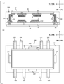
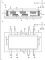
- FIG.1 (a) is a longitudinal cross-sectional view of the electronic module which can be used by the 1st Embodiment of this invention
- FIG.1 (b) is a top view of the electronic module shown to Fig.1 (a). is there.
- the sealing part is not shown in FIG.1 (b), and the sealing part is not shown in the top view and bottom view also in subsequent drawings.
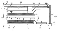
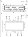
- FIG. 2 is a longitudinal sectional view of an electronic module that can be used in the first embodiment of the present invention, and is a longitudinal sectional view of an electronic module different from the mode shown in FIG. FIG.
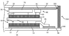
- FIG. 3 is a longitudinal sectional view of an electronic module which can be used in the first embodiment of the present invention, and is a longitudinal sectional view of an electronic module different from the mode shown in FIGS. 1 and 2.
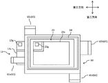
- FIG. 4 is a plan view showing a first connection body and the like that can be used in the first embodiment of the present invention.
- FIG. 5 (a) is a longitudinal sectional view of still another aspect of the electronic module that can be used in the first embodiment of the present invention, and FIG. 5 (b) is the electronic shown in FIG. 5 (a). It is a top view of a module.
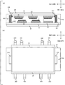
- FIG. 6 (a) is a longitudinal sectional view of an electronic module which can be used in the second embodiment of the present invention, and
- FIG. 6 (b) is a bottom view of the electronic module shown in FIG.
- FIG. 7 (a) is a longitudinal sectional view of an electronic module that can be used in the third embodiment of the present invention
- FIG. 7 (b) is a plan view of the electronic module shown in FIG. 1 (a).
- FIG. 8 (a) is a longitudinal sectional view of an electronic module that can be used in the third embodiment of the present invention
- FIG. 8 (b) is a bottom view of the electronic module shown in FIG. 7 (a).
- FIG. 9 (a) is a longitudinal sectional view of an electronic module that can be used in the fourth embodiment of the present invention
- FIG. 9 (b) is a plan view of the electronic module shown in FIG. 9 (a). is there.
- FIG. 9 (a) is a longitudinal sectional view of an electronic module that can be used in the fourth embodiment of the present invention
- FIG. 9 (b) is a plan view of the electronic module shown in FIG. 9 (a). is there.
- FIG. 10 (a) is a longitudinal sectional view of an electronic module that can be used in the fifth embodiment of the present invention
- FIG. 10 (b) is a plan view of the electronic module shown in FIG. 10 (a). is there.
- FIG. 11 is a plan view showing a lead frame which can be used in the sixth embodiment of the present invention, and virtually shows a position where the second substrate is to be disposed and a planned cutting line.
- FIG. 12 is a plan view showing an aspect in which the first positioning member is formed by cutting and bending the lead frame shown in FIG.
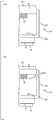
- FIG. 13 (a) is a longitudinal sectional view showing a positioning portion formed of a lead frame, which can be used in the sixth embodiment of the present invention
- FIG. 13 (b) is a sixth embodiment of the present invention.
- FIG. 13 (a) is a longitudinal sectional view showing a positioning portion formed of a lead frame, which can be used in the sixth embodiment of the present invention
- FIG. 13 (b) is a sixth embodiment of the present invention.
- FIG. 16 is a longitudinal sectional view showing another aspect of the positioning part configured of a lead frame, which can be used in the embodiment of FIG.
- FIG. 14 is a plan view showing a first connection body that can be used in the seventh embodiment of the present invention.
- FIG. 15 is a longitudinal sectional view for showing a second connection body that can be used in the eighth embodiment of the present invention.
- first direction the left-right direction
- second direction the front and back direction of the paper
- third direction the front and back direction of the paper
- the electronic module of the present embodiment may have a first electronic unit and a second electronic unit.
- the first electronic unit includes a first substrate 11, a plurality of first conductor layers 12 provided on one side of the first substrate 11, and one side of the first conductor layer 12.
- the first electronic element 13 provided in The first electronic element 13 may be a switching element or a control element.
- the first electronic element 13 may be a MOSFET, an IGBT or the like.
- Each of the first electronic element 13 and the second electronic element 23 described later may be composed of a semiconductor element, and the semiconductor material may be silicon, silicon carbide, gallium nitride or the like.
- the surface on the other side of the first electronic element 13 may be connected to the first conductor layer 12 via the conductive adhesive 5 such as solder.
- the second electronic unit includes a second substrate 21, a plurality of second conductor layers 22 provided on the other side of the second substrate 21, and the other side of the second conductor layer 22.
- the second electronic device 23 provided in The surface on one side of the second electronic element 23 may be connected to the second conductor layer 22 via the conductive adhesive 5 such as solder.
- a first connection body 60 may be provided on one side of the first electronic element 13.
- the first connection body 60 may be connected to the surface on one side of the first electronic element 13 via the conductive adhesive 5 (not shown in FIG. 2) such as solder.
- the first connection body 60 is provided between the first electronic element 13 and the second electronic element 23, and the first electronic element 13 and the second electronic element 23 are in the first connection. It will be electrically connected by the body 60.
- a second connecting body 70 may be provided on the other side of the second conductor layer 22.
- the second connection body 70 may be connected to the one surface of the second electronic element 23 and the other surface of the second conductor layer 22 via the conductive adhesive 5 such as a solder.
- the first electronic element 13 is fixed to the first substrate 11 by being connected to the first conductor layer 12 provided on the first substrate 11 via the conductive adhesive 5.
- the second electronic element 23 is fixed to the second electronic element 23 by being connected to the second conductor layer 22 provided on the second substrate 21 via the conductive adhesive 5. become.
- the second electronic element 23 may be a switching element or a control element.
- the second electronic element 23 may be a MOSFET, an IGBT, or the like.
- the first connection body 60 may have a first head portion 61 and a first pillar portion 62 extending from the first head portion 61 to the other side.
- the second connection body 70 may have a second head portion 71 and a second pillar portion 72 extending from the second head portion 71 to the other side.
- the first connector 60 may have a substantially T-shaped cross section, and the second connector 70 may have a substantially T-shaped cross section.
- a ceramic substrate, an insulating resin layer or the like can be adopted as the first substrate 11 and the second substrate 21.
- a material containing Ag or Cu as a main component can be used other than solder.
- a metal such as Cu can be used.
- the substrates 11 and 12 provided with the conductor layers 12 and 22 it is also possible to use a metal substrate subjected to circuit patterning.
- a metal substrate subjected to circuit patterning can be used as the substrates 11 and 21. In this case, the substrates 11 and 21 also serve as the conductor layers 12 and 22, respectively.
- the electronic module includes the first electronic element 13, the second electronic element 23, the first connecting body 60, the second connecting body 70, the first conductor layer 12, and the second conductor as described above.
- You may have the sealing part 90 comprised from sealing resin etc. which seals layer 22 grade
- the other side of the first substrate 11 may be provided with a first heat radiation plate 19 made of a copper plate or the like.
- a second heat dissipation plate 29 formed of a copper plate or the like may be provided.
- the first conductor layer 12 or the second conductor layer 22 may be connected to the terminal portion 100, and the tip end side of the terminal portion 100 is exposed to the outside of the sealing portion 90, and can be connected to an external device. Good.
- the terminal portion 100 shown in FIG. 1B is bent to one side, and the tip is extended to the front surface side of the paper surface of FIG. 1B.
- a positioning portion 200 may be provided which extends from the first substrate 11 to one side and abuts on the peripheral portion of the second substrate 21.
- the positioning unit 200 may have a plurality of first positioning members 210. In the present embodiment, the following description will be made using a mode in which four first positioning members 210 are provided, but the present invention is not limited to this.
- the first positioning members 210 may be two, three or five. More than one may be provided.
- Each of the first substrate 11 and the second substrate 21 may be substantially rectangular. As shown in FIG. 1B, the first positioning member 210 may be provided to correspond to each side (four sides). However, the first positioning member 210 may be provided to correspond to two sides or three sides, and two or more first positioning members 210 may be provided for one side (for example, a long side). One positioning member 210 may be provided.
- the first positioning member 210 may be provided at the center of each side.
- the “central portion” means the central region in the case where it is equally divided into five along the side.
- substantially rectangular means a quadrilateral having two pairs of opposite sides, and for example, the corner may be rounded.
- the first guide member 210 does not have to be provided at the center of each side of the second substrate 21, and only a part of the plurality of first positioning members 210 is the center of the side of the second substrate 21. And the remaining portion may be provided on the corner side other than the central portion of the side of the second substrate 21.
- each of the 1st positioning members 210 of the positioning part 200 may have the 1st protrusion part 211 which protruded in the periphery inward.
- the first protrusion 211 may be in contact with the other surface of the second substrate 21. As shown in FIGS. 2 and 3, the first protrusion 211 may abut on the peripheral portion of the second conductor layer 22.
- the first protrusion 211 is not in contact with the other surface of the second substrate 21, but as shown in FIG. 5, the first protrusion 211 is in contact with the other surface of the second conductor layer 22. It may be
- the first projecting portion 211 does not have to be provided on each of the first positioning members 210, and the first projecting portion 211 is provided only on a part of the plurality of first positioning members 210, and the remaining portion is provided on the remaining portion.
- the first positioning member 210 may not be provided.
- the first projecting portion 211 is provided on two first positioning members 210 for supporting a pair of opposing sides (for example, the long side) of the second substrate 21 and another pair of sides (for example, the short sides)
- the first protrusion 211 may not be provided on the first positioning member 210 supporting the
- the first protrusion 211 may not be provided. In this case, only the positioning in the surface direction of the second substrate 21 with respect to the first substrate 11 is performed by the positioning unit 200.
- the first positioning member 210 of the positioning unit 200 may be fixed to the first substrate 11 using the bonding material 240.
- the melting point of the bonding material 240 may be higher than the melting point of the conductive adhesive 5.
- the first positioning member 210 of the positioning unit 200 may be bonded and fixed to the surface (upper surface in FIG. 1) of one side of the first substrate 11 by the bonding material 240.
- the size in the surface direction of the first substrate 11 may be larger than the surface direction of the second substrate 21.
- the first positioning member 210 may be bonded to the first conductor layer 12 by the bonding material 240 (see FIG. 5), and also in this case, the first positioning member 210 is the surface on one side of the first substrate 11 Will be fixed against.
- a first groove portion 64 may be provided on the surface on one side of the first head portion 61.
- the first groove portion 64 is provided outward of the peripheral edge of the first column portion 62 in a plan view (surface direction), but may be provided at a part of the peripheral edge outward. It may be provided on the entire outer periphery.
- a conductive adhesive 5 such as a solder may be provided on the surface on one side of the first head portion 61 and inside the periphery of the first groove 64, and the second electron may be provided via the conductive adhesive 5.
- An element 23 may be provided.
- a connector 85 connected to a terminal such as a second gate terminal 23 g described later of the second electronic element 23 may be used.
- the present invention is not limited to such an aspect, and a third connection body 80 as shown in FIG. 3 may be used.
- the third connector 80 may have a third head 81 and a third pillar 82 extending from the third head 81 to the other side.
- Third connecting body 80 is connected to the other surface of second conductive layer 22 and the surface on one side of second electronic element 23 through conductive adhesive 5 (not shown in FIG. 3) such as solder. May be
- the first electronic element 13 may be exposed from the first head portion 61.
- the first gate terminal 13g or the like may be provided in a portion exposed from the first head portion 61 in a plan view.
- the second electronic element 23 is a switching element such as a MOSFET, the second gate terminal 23g or the like may be provided on the surface on one side.
- the first electronic device 13 shown in FIG. 4 has a first gate terminal 13g and a first source terminal 13s on one side, and the second electronic device 23 has a second gate terminal 23g and a second on the one side. It has two source terminals 23s.
- the second connector 70 is connected to the second source terminal 23s of the second electronic element 23 via the conductive adhesive 5, and the connector 85 is electrically conductive to the second gate terminal 23g of the second electronic element 23. It may be connected via an adhesive 5.
- the first connection body 60 connects the first source terminal 13s of the first electronic element 13 and the second drain terminal provided on the other side of the second electronic element 23 through the conductive adhesive 5, Good.
- the first drain terminal provided on the other side of the first electronic element 13 may be connected to the first conductor layer 12 via the conductive adhesive 5.
- the first gate terminal 13 g of the first electronic element 13 is connected to the connector 95 (see FIGS. 2 and 3) via the conductive adhesive 5, and the connector 95 is connected to the first via the conductive adhesive 5. It may be connected to the conductor layer 12.
- the second electronic element 23 mounted on the first connecting member 60 is used as a control element with low heat generation, It is also conceivable to make the electronic element 13 a switching element. Conversely, it is also conceivable to use the second electronic element 23 mounted on the first connection body 60 as a switching element and the first electronic element 13 as a control element with low heat generation.
- the bonding between the terminal portion 100 and the conductor layers 12 and 22 may be performed not only by using a conductive adhesive 5 such as a solder but also by laser welding or ultrasonic bonding.
- a jig is separately used.
- the second substrate 21 can be positioned in the planar direction with respect to the first substrate 11 and, in turn, the first substrate 11 and the second substrate 21 can be kept parallel. That is, positioning the second substrate 21 in the surface direction with respect to the first substrate 11 can prevent the second substrate 21 from shifting in the surface direction with respect to the first substrate 11, and as a result, the first substrate 11 can be prevented.
- the second substrate 21 can be prevented from tilting in the first direction.
- the jig in view of keeping the first substrate 11 and the second substrate 21 in parallel, it is necessary to make the size in the plane direction of the jig and the substrates 11 and 21 approximately the same.
- the jig when the jig is enlarged in this manner, the jig itself may be stretched by the application of heat as in the case of remelting (reflowing) of the conductive adhesive 5 such as a solder, for example.
- the jig when the jig itself positions the substrates 11 and 21 in the first direction as well, if the jig itself is stretched, it also causes the substrates 11 and 21 to be warped or distorted.
- the size of the positioning unit 200 itself is not so large, so the amount of expansion does not become so large even if heat is applied. Therefore, it is possible to prevent the substrates 11 and 21 from being warped or distorted.
- the dimensional tolerances of the jigs may be set loose to prevent warpage and distortion of the substrates 11 and 21. It becomes difficult to maintain the parallelism between the substrates 21.
- the positioning portion 200 as in the present embodiment it is possible to prevent the substrates 11 and 21 from being warped or distorted while maintaining the parallelism between the first substrate 11 and the second substrate 21. It is beneficial in point. Note that these effects become particularly large when the size in the surface direction of the substrates 11 and 21 becomes large. Therefore, the aspect of the present embodiment is particularly useful in the aspect in which the plurality of electronic elements 13 and 23 are provided in the surface direction.
- the positioning unit 200 has a plurality of first positioning members 210, more accurate positioning becomes possible by using the plurality of first positioning members 210.
- the second substrate 21 has a substantially rectangular shape and the first positioning member 210 is provided to correspond to each side (four sides), positioning can be performed on each side of the second substrate 21. It is possible to more reliably prevent the second substrate 21 from shifting in the surface direction with respect to the first substrate 11.
- the second substrate 21 can be positioned with respect to the first substrate 11 in a well-balanced manner.
- the second substrate 21 can also be positioned in the first direction, and the distance between the second substrate 21 and the first substrate 11 can be set. It can be made more than a certain amount.
- the ability to perform positioning in the first direction in this way makes it possible to make the thickness of the conductive adhesive 5 such as solder used to connect the electronic elements 13 and 23 equal to or greater than a certain value, thereby enhancing reliability. It is useful in that it can be done.
- the second substrate 21 can also be positioned more reliably in the first direction.
- the first projecting portion 211 may abut on the other side surface of the second substrate 21, and as shown in FIG. It may be in contact with the other side of the layer 22.
- the substrates 11 and 21 When the size in the surface direction of the substrates 11 and 21 is increased, the substrates are likely to be warped or distorted. In this respect, provision of the first projecting portion 211 as described above is advantageous in that warpage and distortion of the substrate can be prevented.
- the first projecting portion 211 abuts on the other surface of the second substrate 21 and abuts on the peripheral portion of the second conductor layer 22, the first projecting portion 211 Is also advantageous in that positioning in the plane direction of the second substrate 21 can be performed.
- the first positioning member 210 is fixed to the first substrate 11 using the bonding material 240, only the first positioning member 210 needs to be attached to the first substrate 11 used from before. It is useful. If the melting point of the bonding material 240 is higher than the melting point of the conductive adhesive 5 such as solder used for connection in the electronic module, the process of remelting the conductive adhesive 5 is Even in the case of use, it is possible to prevent the fixing of the first positioning member 210 to the first substrate 11 from being loosened. For this reason, when the conductive adhesive 5 is remelted, it can prevent that the position of the 2nd board
- the positioning unit 200 is fixed to the surface on one side of the first substrate 11, it is only necessary to fix the positioning unit 200 on the surface on one side of the first substrate 11, thereby facilitating the manufacture. It is useful.
- the positioning unit 200 does not have to be fixed to the surface on one side of the first substrate 11.
- the positioning unit 200 may be fixed to the side surface of the first substrate 11 via the bonding material 240.
- the first connection body 60 when the first connection body 60 as shown in FIGS. 2 and 3 is employed, the first connection body 60 causes the first connection body 60 to be between the first substrate 11 and the second substrate 23 inside the peripheral edge of the substrates 11 and 21. Distance can be kept above a certain value. For this reason, even in the case of employing the large substrates 11 and 21 in the plane direction, it is advantageous in that it is possible to more reliably prevent the substrates 11 and 21 from being warped or distorted.
- the distance between the first substrate 11 and the second substrate 23 can be maintained at a predetermined value or more inside the peripheral edge of the substrates 11 and 21. For this reason, even in the case of employing the large substrates 11 and 21 in the plane direction, it is advantageous in that it is possible to more reliably prevent the substrates 11 and 21 from being warped or distorted.
- the 1st connection body 60 and the 2nd connection body 70 are used is shown in FIG.2 and FIG.3, the 1st connection body 60 and the 2nd connection body 70 may not be provided. (Refer FIG. 1 (a) and FIG. 5 (a)).
- the positioning portion 200 extends from the first substrate 11 to one side and abuts on the peripheral portion of the second substrate 21, but in the present embodiment, as shown in FIG.
- the positioning portion 200 extends from the second substrate 21 to the other side and abuts on the peripheral portion of the first substrate 11.
- the other configuration is the same as that of the first embodiment, and all aspects described in the first embodiment can be adopted.
- the members described in the first embodiment will be described using the same reference numerals.
- the positioning unit 200 may have a plurality of second positioning members 220.
- the second positioning member 220 may be provided with a second protrusion 221.
- the second protrusion 221 may abut on one surface of the first substrate 11. Further, the second protrusion 221 may abut on the peripheral portion of the first conductor layer 12.
- the second positioning member 220 may be fixed to the other surface of the second substrate 21.
- the size in the surface direction of the second substrate 21 may be larger than the surface direction of the first substrate 11.
- a first positioning member 210 extending from the first substrate 11 to one side and in contact with the peripheral edge of the second substrate 21 and the other side from the second substrate 21
- both of the second positioning members 220 that extend in contact with the peripheral edge of the first substrate 11 are used.
- the other configuration is the same as that of each of the above-described embodiments, and any of the aspects described in each of the above-described embodiments can be adopted.
- the first positioning member 210 is not limited to the first The protrusion 211 may be provided, and the second positioning member 220 may be provided with a second protrusion 221.
- the first protrusion 211 provided on the first positioning member 210 may abut on the other surface of the second substrate 21. Also, the first protrusion 211 may abut on the peripheral portion of the second conductor layer 22.
- the second protrusion 221 provided on the second positioning member 220 may abut on one surface of the first substrate 11. Further, the second protrusion 221 may abut on the peripheral portion of the first conductor layer 12.
- two first positioning members 210 and two second positioning members 220 may be used.
- the pair of first positioning members 210 may be provided on the opposite side of the first substrate 11, and the pair of second positioning members 220 may be provided on the opposite side of the second substrate 21.
- two first positioning members 210 may be provided on adjacent sides of the first substrate 11, and two second positioning members 220 may be provided on adjacent sides of the second substrate 21, for example. It is also good.
- the first positioning member 210 may be fixed to one surface of the first substrate 11, and the second positioning member 220 may be fixed to the other surface of the second substrate 21.
- the length of the second substrate 21 is shorter than the length of the first substrate 11 in the surface direction (the second direction) in which the two first positioning members 210 are provided, as shown in FIG.
- the length of the first substrate 11 may be shorter than the length of the second substrate 21 in the surface direction (third direction) in which the two second positioning members 220 are provided.
- the first substrate 11 and the second substrate 21 are inclined in the surface direction. It may be displaced in the direction (direction between the second direction and the third direction). In this case, the two first positioning members 210 abut on adjacent two sides of the second substrate 21 and the two second positioning members 220 abut on adjacent two sides of the first substrate 11. Become.
- relative positioning between the first substrate 11 and the second substrate 21 can be performed using each of the first positioning member 210 and the second positioning member 220.
- the shape of the tip of the positioning member 210, 220 is not particularly referred to, but in the present embodiment, as shown in FIG. 9, the tip of the positioning member 210, 220 of the positioning unit 200.
- the part is tapered.
- any of the aspects described in the above embodiments can be adopted.
- Positioning in the surface direction can be performed more easily by adopting an aspect in which the tip end portions of the positioning members 210 and 220 of the positioning portion 200 have a tapered shape as in the present embodiment. More specifically, in the aspect as in the first embodiment, in the case where the end portion of the first positioning member 210 has a tapered shape, the second position relative to the first substrate 11 is selected. When positioning the substrate 21, the second substrate 21 is shifted in the surface direction along the leading end of the first positioning member 210 only by bringing the second substrate 21 close to the first substrate 11 in the first direction. Positioning can be performed. In the mode as in the second embodiment, in the case where the end portion of the second positioning member 220 is tapered, the first substrate 11 is positioned with respect to the second substrate 21.
- the first substrate 11 is shifted in the surface direction along the front end of the second positioning member 220 only by bringing the first substrate 11 close to the second substrate 21 in the first direction. it can.
- the aspect as in the third embodiment is adopted.
- the distance between the second positioning members 220 provided on opposing sides is smaller than the length in the width direction of the substrates 11 and 21 corresponding to the opposing sides. ing.
- the tapered portions of the positioning members 210 and 220 abut the peripheral edge portions of the substrates 11 and 21, and positioning in the surface direction and the first direction becomes possible.
- the distance between the positioning members 210 and 220 provided on opposing sides is equal to or larger than the size of the substrates 11 and 21, and the protrusions 211 and 221 are formed on the positioning members 210 and 220. Is provided.
- the other configuration is the same as that of the fourth embodiment.
- any of the aspects described in the above embodiments can be adopted. About the member demonstrated by said each embodiment, it demonstrates using the same code
- the substrates 11 and 21 are guided by the tapered portions of the positioning members 210 and 220, and finally the planar direction and the first direction of the substrates 11 and 21 by the projecting portions 211 and 221. It can be positioned with Specifically, in the aspect as in the first embodiment, when the tip of the first positioning member 210 is tapered and the first protrusion 211 is provided, the first substrate 11 is provided. When the second substrate 21 is positioned with respect to the first substrate 11, the second substrate 21 may be positioned along the tip of the first positioning member 210 simply by bringing the second substrate 21 closer to the first substrate 11 in the first direction.
- the second substrate 21 may be positioned in the plane direction and the first direction with respect to the first substrate 11 by being shifted in the plane direction and the other surface of the second substrate 21 being supported by the first protrusion 211. it can.
- the first substrate relative to the second substrate 21 is provided in the case where the tip of the second positioning member 220 is tapered and the second protrusion 221 is provided.
- the first substrate 11 is shifted in the surface direction along the tip of the second positioning member 220 simply by bringing the first substrate 11 closer to the second substrate 21 in the first direction, The surface on one side of the first substrate 11 is supported by the second protrusion 221, and the first substrate 11 can be positioned with respect to the second substrate 21 in the surface direction and the first direction.
- the aspect as in the third embodiment is adopted.
- the positioning portion 200 is fixed to the substrates 11 and 21 by the bonding material 240.
- the positioning is performed by the lead frame 300 for forming the terminal portion 100 and the like.
- the part 200 is comprised (refer FIG.11 and FIG.12).
- any of the aspects described in the above embodiments can be adopted.
- the positioning part 200 is formed by cutting the lead frame 300 at an appropriate place and then bending it. More specifically, the positioning part 200 is formed by cutting the lead frame 300 at a planned cutting position (see FIG. 11) and bending it to one side or the other side (see FIG. 12).
- Positioning portion 200 of the present embodiment is provided with a lead frame proximal end extending in the surface direction and a lead frame provided at the lead frame proximal end via a lead frame bending portion and extending to one side or the other side. It may have an extension.
- the first lead frame proximal end 217 extending in the surface direction and the first lead frame proximal end 217 are provided via the lead frame bending portion 218 and extend to one side And a first lead frame extension portion 216.
- the lead frame 300 may be struck or pressed on the surface opposite to the location where the protrusions 211 and 221 are provided. By striking or pressing the lead frame 300 in this manner, the protrusions 211 and 221 are formed. In this case, as shown in FIG. 13 (b), a recess 211a corresponding to the protrusion 211 is formed.
- first guide member 210 is described using the aspect formed of the lead frame 300 in FIGS. 11 to 13, as described above, all the aspects described in each of the above embodiments are adopted.
- the second guide member 220 may be formed by the lead frame 300.
- the positioning portion 200 can be formed using the lead frame 300, which is advantageous in that the bonding material 240 need not be used.
- the first connection body 60 having a substantially T-shaped cross section is used. However, as shown in FIG. , And four supporting portions 65 (65a to 65d) extending from the other side.
- the support 65 is in contact with the first conductor layer 12 or the first substrate 11. Also in the present embodiment, any of the aspects described in the above embodiments can be adopted. About the member demonstrated by said each embodiment, it demonstrates using the same code
- the present embodiment is described using an aspect in which four supporting portions 65 are used, the present invention is not limited to this, and one, two, three, or five or more supporting portions 65 may be used. .
- the second electronic element is mounted when the second electronic element 23 is mounted or after the second electronic element 23 is mounted.
- the weight of 23 can prevent the first connection body 60 from being inclined.
- the heat dissipation can be enhanced by the support portion 65 being in contact with the first substrate 11 or the first conductor layer 12 as described above.
- the support portion 65 abuts on the first conductor layer 12, it is advantageous in that the heat dissipation effect can be further enhanced.
- the positioning in the first direction can be performed more reliably inside the peripheral edges of the substrates 11 and 21.
- the first connecting body 60 employing the projecting portions 211 and 221 and the plurality of supporting portions 65 positioning in the first direction at the peripheral portion of the substrates 11 and 21 by the projecting portions 211 and 221
- positioning in the first direction at the peripheral portion of the substrates 11 and 21 by the projecting portions 211 and 221 It is possible to position in the first direction inward the peripheral edge of the substrates 11 and 21 by the first connecting member 60 having the plurality of support portions 65 while performing the above. For this reason, even in the case of employing the large substrates 11 and 21 in the plane direction, it is advantageous in that it is possible to more reliably prevent the substrates 11 and 21 from being warped or distorted.
- the distal end portions of the positioning members 210 and 220 are tapered, and the distance between the second positioning members 220 provided on the opposite sides is smaller than that of the substrates 11 and 21.
- the first connecting member 60 performs the first inward of the periphery of the substrates 11 and 21 while performing positioning in the first direction at the periphery of the substrates 11 and 21 by the tip end of the positioning members 210 and 220. It can be positioned in one direction.
- connection body 70 in which the cross section having the second column portion 72 has a substantially T shape, but in the present embodiment, as shown in FIG. 70 has an extending portion 75 (75a, 75b) extending from the second head portion 71 to the other side. Also in the present embodiment, any of the aspects described in the above embodiments can be adopted. About the member demonstrated by said each embodiment, it demonstrates using the same code
- extension parts 75 are used, the present invention is not limited to this, and one or more extension parts 75 may be used.
- the extension portion 75 since the extension portion 75 is provided, the heat from the second electronic element 23 can be efficiently dissipated, and a high heat dissipation effect can be realized also by the second connection body 70. . Further, in the case where a plurality of extending portions 75 are provided as in the present embodiment, it is advantageous in that a higher heat dissipation effect can be realized.
- the positioning in the first direction can be performed more reliably inside the peripheral edges of the substrates 11 and 21.
- the peripheral portions of the substrates 11 and 21 by the projecting portions 211 and 221 have a first direction. While positioning is performed, positioning can be performed in the first direction inside the periphery of the substrates 11 and 21 by the second connection body 70 having the plurality of extension portions 75. For this reason, even in the case of adopting the large substrates 11 and 21 in the plane direction, it is advantageous in that it is possible to more reliably prevent the substrate from being warped or distorted.
- the distal end portions of the positioning members 210 and 220 are tapered, and the distance between the second positioning members 220 provided on the opposite sides is smaller than that of the substrates 11 and 21.
- the second connecting member 70 performs inward of the periphery of the substrates 11 and 21 while performing positioning in the first direction at the periphery of the substrates 11 and 21 by the front end portions of the positioning members 210 and 220. It can be positioned in one direction.
Landscapes
- Combinations Of Printed Boards (AREA)
- Physics & Mathematics (AREA)
- Geometry (AREA)
Abstract
電子モジュールは、第一基板11と、前記第一基板11の一方側に設けられた第一電子素子13と、前記第一電子素子13の一方側に設けられた第二基板21と、前記第一基板11から一方側に延びて前記第二基板21の周縁部に当接する、又は、前記第二基板21から他方側に延びて前記第一基板11の周縁部に当接する位置決め部200と、を有する。
Description
本発明は、第一基板と、第一基板の一方側に設けられた第二基板とを有する電子モジュールに関する。
複数の電子素子が封止樹脂内に設けられた電子モジュールが従来から知られている(例えば特開2014-45157号参照)。このような電子モジュールでは、第一基板と、第一基板の一方側に設けられた電子素子と、電子素子の一方側に配置された第二基板とが設けられることがある。
このような第一基板と第二基板を採用する場合、特に第一基板と第二基板の面方向の大きさが大きくなる場合には、第一基板と第二基板との面方向でのずれを防止し、ひいては第一基板と第二基板とを平行に保つために治具を用いている。
本発明は、治具を用いなくても第一基板と第二基板とを平行に保つことができる電子モジュールを提供する。
本発明による電子モジュールは、
第一基板と、
前記第一基板の一方側に設けられた電子素子と、
前記電子素子の一方側に設けられた第二基板と、
前記第一基板から一方側に延びて前記第二基板の周縁部に当接する、又は、前記第二基板から他方側に延びて前記第一基板の周縁部に当接する位置決め部と、
を備えてもよい。
第一基板と、
前記第一基板の一方側に設けられた電子素子と、
前記電子素子の一方側に設けられた第二基板と、
前記第一基板から一方側に延びて前記第二基板の周縁部に当接する、又は、前記第二基板から他方側に延びて前記第一基板の周縁部に当接する位置決め部と、
を備えてもよい。
本発明による電子モジュールにおいて、
前記位置決め部は、周縁内方に突出した突出部を有し、
前記位置決め部が前記第一基板から一方側に延びて前記第二基板の周縁部に当接する場合には、前記突出部は前記第二基板の他方側の面に当接し、
前記位置決め部が前記第二基板から他方側に延びて前記第一基板の周縁部に当接する場合には、前記突出部は前記第一基板の一方側の面に当接してもよい。
前記位置決め部は、周縁内方に突出した突出部を有し、
前記位置決め部が前記第一基板から一方側に延びて前記第二基板の周縁部に当接する場合には、前記突出部は前記第二基板の他方側の面に当接し、
前記位置決め部が前記第二基板から他方側に延びて前記第一基板の周縁部に当接する場合には、前記突出部は前記第一基板の一方側の面に当接してもよい。
本発明による電子モジュールは、
前記第一基板の一方側に設けられた第一導体層と、
前記第二基板の他方側に設けられた第二導体層と、をさらに備え、
前記位置決め部が前記第一基板から一方側に延びて前記第二基板の周縁部に当接する場合には、前記突出部は前記第二導体層の周縁部に当接し、
前記位置決め部が前記第二基板から他方側に延びて前記第一基板の周縁部に当接する場合には、前記突出部は前記第一導体層の周縁部に当接してもよい。
前記第一基板の一方側に設けられた第一導体層と、
前記第二基板の他方側に設けられた第二導体層と、をさらに備え、
前記位置決め部が前記第一基板から一方側に延びて前記第二基板の周縁部に当接する場合には、前記突出部は前記第二導体層の周縁部に当接し、
前記位置決め部が前記第二基板から他方側に延びて前記第一基板の周縁部に当接する場合には、前記突出部は前記第一導体層の周縁部に当接してもよい。
本発明による電子モジュールにおいて、
前記位置決め部が前記第一基板から一方側に延びて前記第二基板の周縁部に当接する場合には、前記位置決め部は前記第一基板の一方側の面に対して固定され、
前記位置決め部が前記第二基板から他方側に延びて前記第一基板の周縁部に当接する場合には、前記位置決め部は前記第二基板の他方側の面に対して固定されてもよい。
前記位置決め部が前記第一基板から一方側に延びて前記第二基板の周縁部に当接する場合には、前記位置決め部は前記第一基板の一方側の面に対して固定され、
前記位置決め部が前記第二基板から他方側に延びて前記第一基板の周縁部に当接する場合には、前記位置決め部は前記第二基板の他方側の面に対して固定されてもよい。
本発明による電子モジュールにおいて、
前記位置決め部が前記第一基板から一方側に延びて前記第二基板の周縁部に当接する場合には、前記位置決め部は前記第一基板に接合材を用いて固定され、
前記位置決め部が前記第二基板から他方側に延びて前記第一基板の周縁部に当接する場合には、前記位置決め部は前記第二基板に接合材を用いて固定され、
前記電子素子は導電性接着剤を用いて前記第一基板又は前記第二基板に対して固定され、
前記接合材の融点は前記導電性接着剤の融点よりも高くてもよい。
前記位置決め部が前記第一基板から一方側に延びて前記第二基板の周縁部に当接する場合には、前記位置決め部は前記第一基板に接合材を用いて固定され、
前記位置決め部が前記第二基板から他方側に延びて前記第一基板の周縁部に当接する場合には、前記位置決め部は前記第二基板に接合材を用いて固定され、
前記電子素子は導電性接着剤を用いて前記第一基板又は前記第二基板に対して固定され、
前記接合材の融点は前記導電性接着剤の融点よりも高くてもよい。
本発明による電子モジュールにおいて、
前記位置決め部はリードフレームで構成され、
前記位置決め部は、面方向で延在するリードフレーム基端部と、前記リードフレーム基端部にリードフレーム屈曲部を介して設けられ、一方側又は他方側に延在するリードフレーム延在部とを有してもよい。
前記位置決め部はリードフレームで構成され、
前記位置決め部は、面方向で延在するリードフレーム基端部と、前記リードフレーム基端部にリードフレーム屈曲部を介して設けられ、一方側又は他方側に延在するリードフレーム延在部とを有してもよい。
本発明による電子モジュールにおいて、
前記位置決め部の先端部はテーパー形状となってもよい。
前記位置決め部の先端部はテーパー形状となってもよい。
本発明による電子モジュールにおいて、
前記電子素子は、第一電子素子と、前記第一電子素子の一方側に設けられた第二電子素子と、を有し、
前記第一電子素子と前記第二電子素子との間に、前記第一電子素子と前記第二電子素子とを電気的に接続する第一接続体が設けられてもよい。
前記電子素子は、第一電子素子と、前記第一電子素子の一方側に設けられた第二電子素子と、を有し、
前記第一電子素子と前記第二電子素子との間に、前記第一電子素子と前記第二電子素子とを電気的に接続する第一接続体が設けられてもよい。
本発明の一態様として、第一基板から一方側に延びて第二基板の周縁部に当接する、又は、第二基板から他方側に延びて第一基板の周縁部に当接する位置決め部が設けられている態様を採用する場合には、治具を用いなくても第一基板と第二基板との面方向でのずれを防止し、ひいては第一基板と第二基板とを平行に保つことができる。
第1の実施の形態
《構成》
本実施の形態において、「一方側」は図1(a)の上方側を意味し、「他方側」は図1(a)の下方側を意味する。図1(a)の上下方向を「第一方向」と呼び、左右方向を「第二方向」と呼び、紙面の表裏方向を「第三方向」と呼ぶ。第二方向及び第三方向を含む面内方向を「面方向」といい、一方側から見た場合には「平面視」という。
《構成》
本実施の形態において、「一方側」は図1(a)の上方側を意味し、「他方側」は図1(a)の下方側を意味する。図1(a)の上下方向を「第一方向」と呼び、左右方向を「第二方向」と呼び、紙面の表裏方向を「第三方向」と呼ぶ。第二方向及び第三方向を含む面内方向を「面方向」といい、一方側から見た場合には「平面視」という。
本実施の形態の電子モジュールは、第一電子ユニットと、第二電子ユニットとを有してもよい。
図1(a)に示すように、第一電子ユニットは、第一基板11と、第一基板11の一方側に設けられた複数の第一導体層12と、第一導体層12の一方側に設けられた第一電子素子13と、を有してもよい。第一電子素子13はスイッチング素子であってもよいし、制御素子であってもよい。第一電子素子13がスイッチング素子である場合には、第一電子素子13はMOSFETやIGBT等であってもよい。第一電子素子13及び後述する第二電子素子23の各々は半導体素子から構成されてもよく、半導体材料としてはシリコン、炭化ケイ素、窒化ガリウム等であってもよい。第一電子素子13の他方側の面は第一導体層12とはんだ等の導電性接着剤5を介して接続されてもよい。
図1(a)に示すように、第二電子ユニットは、第二基板21と、第二基板21の他方側に設けられた複数の第二導体層22と、第二導体層22の他方側に設けられた第二電子素子23と、を有してもよい。第二電子素子23の一方側の面は第二導体層22とはんだ等の導電性接着剤5を介して接続されてもよい。
図2に示すように、第一電子素子13の一方側には第一接続体60が設けられてもよい。第一接続体60は第一電子素子13の一方側の面とはんだ等の導電性接着剤5(図2では図示せず)を介して接続されてもよい。図2に示す態様では、第一電子素子13と第二電子素子23との間に第一接続体60が設けられることになり、第一電子素子13と第二電子素子23とが第一接続体60によって電気的に接続されることになる。
図2に示すように、第二導体層22の他方側には第二接続体70が設けられてもよい。第二接続体70は第二電子素子23の一方側の面及び第二導体層22の他方側の面とはんだ等の導電性接着剤5を介して接続されてもよい。
なお、第一電子素子13は、第一基板11に設けられた第一導体層12に導電性接着剤5を介して接続されることで、第一基板11に対して固定されることになる。同様に、第二電子素子23は、第二基板21に設けられた第二導体層22に導電性接着剤5を介して接続されることで、第二電子素子23に対して固定されることになる。
第二電子素子23はスイッチング素子であってもよいし、制御素子であってもよい。第二電子素子23がスイッチング素子である場合には、第二電子素子23はMOSFETやIGBT等であってもよい。
図2に示すように、第一接続体60は、第一ヘッド部61と、第一ヘッド部61から他方側に延びた第一柱部62を有してもよい。第二接続体70は、第二ヘッド部71と、第二ヘッド部71から他方側に延びた第二柱部72を有してもよい。第一接続体60は断面が略T字形状となり、第二接続体70も断面が略T字形状となってもよい。
第一基板11及び第二基板21としては、セラミック基板、絶縁樹脂層等を採用することができる。導電性接着剤5としては、はんだの他、AgやCuを主成分とする材料を用いることもできる。第一接続体60及び第二接続体70の材料としてはCu等の金属を用いることができる。なお、導体層12,22が設けられた基板11,12としては、回路パターニングを施した金属基板を用いることもできる。なお、基板11,21としては例えば回路パターニングを施した金属基板を用いることもでき、この場合には、基板11,21が導体層12,22を兼ねることになる。
図1(a)に示すように、電子モジュールは、前述した、第一電子素子13、第二電子素子23、第一接続体60、第二接続体70、第一導体層12、第二導体層22等を封止する封止樹脂等から構成される封止部90を有してもよい。第一基板11の他方側には銅板等から構成される第一放熱板19が設けられてもよい。第二基板21の一方側には銅板等から構成される第二放熱板29が設けられてもよい。
第一導体層12又は第二導体層22は端子部100と接続されてもよく、端子部100の先端側は封止部90の外方に露出して、外部装置と接続可能となってもよい。図1(b)に示す端子部100は一方側に屈曲する態様となっており、先端は図1(b)の紙面のおもて面側に延びる態様となっている。
第一基板11から一方側に延びて第二基板21の周縁部に当接する位置決め部200が設けられてもよい。位置決め部200は複数の第一位置決め部材210を有してもよい。本実施の形態では、以下、第一位置決め部材210が4つ設けられている態様を用いて説明するが、これに限られることはなく、第一位置決め部材210は、2つ、3つ又は5つ以上設けられてもよい。
第一基板11及び第二基板21の各々は略矩形状になってもよい。図1(b)に示すように、第一位置決め部材210は各辺(4辺)に対応するようにして設けられてもよい。このような態様に限られることはなく、第一位置決め部材210は2辺又は3辺に対応するように設けられてもよいし、一つの辺(例えば長辺)に対して2つ以上の第一位置決め部材210が設けられてもよい。
第一位置決め部材210は、各辺の中央部に設けられてもよい。本実施の形態において「中央部」とは、辺に沿って5等分した場合の中央領域のことを意味している。本実施の形態において「略矩形状」とは対向する2対の辺を有する四角形のことを意味し、例えば角部が丸みを帯びていてもよい。なお、第一案内部材210は第二基板21の各辺の中央部に設けられている必要はなく、複数設けられた第一位置決め部材210の一部だけが第二基板21の辺の中央部に設けられ、残部は第二基板21の辺の中央部以外の角部側に設けられてもよい。
図1(a)に示すように、位置決め部200の第一位置決め部材210の各々は、周縁内方に突出した第一突出部211を有してもよい。第一突出部211は第二基板21の他方側の面に当接するようになってもよい。図2及び図3に示すように、第一突出部211は第二導体層22の周縁部に当接してもよい。
第一突出部211は第二基板21の他方側の面に当接するのではなく、図5に示すように、第一突出部211は第二導体層22の他方側の面に当接するようになってもよい。
なお、第一突出部211は第一位置決め部材210の各々に設けられている必要はなく、複数設けられた第一位置決め部材210の一部にだけ第一突出部211が設けられ、残部には第一位置決め部材210が設けられてなくてもよい。一例としては、第二基板21の対向する一対の辺(例えば長辺)を支持するための2つの第一位置決め部材210に第一突出部211が設けられ、別の一対の辺(例えば短辺)を支持する第一位置決め部材210には第一突出部211は設けられなくてもよい。
前述したような態様とは異なり、第一突出部211は設けられてなくてもよい。この場合には、位置決め部200によって第一基板11に対する第二基板21の面方向の位置決めだけが行われることになる。
位置決め部200の第一位置決め部材210は接合材240を用いて第一基板11に対して固定されてもよい。接合材240の融点は導電性接着剤5の融点よりも高くなってもよい。
位置決め部200の第一位置決め部材210は第一基板11の一方側の面(図1の上方面)に接合材240によって接着されて固定されてもよい。この態様を採用した場合には、第一基板11の面方向の大きさは第二基板21の面方向よりも大きくなってもよい。なお、第一位置決め部材210は第一導体層12に対して接合材240によって接着されてもよく(図5参照)、この場合にも第一位置決め部材210は第一基板11の一方側の面に対して固定されることになる。
図4に示すように、第一ヘッド部61の一方側の面には第一溝部64が設けられてもよい。第一溝部64は、平面視(面方向)において、第一柱部62の周縁外方に設けられているが、周縁外方の一部に設けられてもよいし、第一柱部62の周縁外方の全部に設けられてもよい。第一ヘッド部61の一方側の面であって、第一溝部64の周縁内方にははんだ等の導電性接着剤5が設けられてもよく、導電性接着剤5を介して第二電子素子23が設けられてもよい。
図2に示すように、第二電子素子23の後述する第二ゲート端子23g等の端子に接続される接続子85が用いられてもよい。このような態様に限られることはなく、図3に示すような第三接続体80が利用されてもよい。第三接続体80は、第三ヘッド部81と、第三ヘッド部81から他方側に延びた第三柱部82を有してもよい。第三接続体80は、はんだ等の導電性接着剤5(図3では図示せず)を介して第二導体層22の他方側の面及び第二電子素子23の一方側の面に接続されてもよい。
図4に示すように、平面視において、第一電子素子13は、第一ヘッド部61から露出する態様となってもよい。第一電子素子13がMOSFET等のスイッチング素子である場合には、平面視において第一ヘッド部61から露出した部分に第一ゲート端子13g等が設けられてもよい。同様に、第二電子素子23がMOSFET等のスイッチング素子である場合には、一方側の面に第二ゲート端子23g等が設けられてもよい。図4に示す第一電子素子13は、一方側の面に第一ゲート端子13gと第一ソース端子13sを有し、第二電子素子23は、一方側の面に第二ゲート端子23gと第二ソース端子23sを有している。この場合、第二接続体70が第二電子素子23の第二ソース端子23sに導電性接着剤5を介して接続され、接続子85が第二電子素子23の第二ゲート端子23gに導電性接着剤5を介して接続されてもよい。また、第一接続体60は第一電子素子13の第一ソース端子13sと第二電子素子23の他方側に設けられた第二ドレイン端子とを導電性接着剤5を介して接続してもよい。第一電子素子13の他方側に設けられた第一ドレイン端子は導電性接着剤5を介して第一導体層12に接続されてもよい。第一電子素子13の第一ゲート端子13gは導電性接着剤5を介して接続子95(図2及び図3参照)に接続され、当該接続子95は導電性接着剤5を介して第一導体層12に接続されてもよい。
第一電子素子13及び第二電子素子23のいずれか一方だけがスイッチング素子の場合には、第一接続体60に載置される第二電子素子23を発熱性の低い制御素子とし、第一電子素子13をスイッチング素子にすることも考えられる。逆に、第一接続体60に載置される第二電子素子23をスイッチング素子とし、第一電子素子13を発熱性の低い制御素子にすることも考えられる。
端子部100と導体層12,22との接合は、はんだ等の導電性接着剤5を利用する態様だけではなく、レーザ溶接を利用してもよいし、超音波接合を利用してもよい。
《作用・効果》
次に、上述した構成からなる本実施の形態による作用・効果の一例について説明する。なお、「作用・効果」で説明するあらゆる態様を、上記構成で採用することができる。
次に、上述した構成からなる本実施の形態による作用・効果の一例について説明する。なお、「作用・効果」で説明するあらゆる態様を、上記構成で採用することができる。
図1(a)等に示すように、第一基板11から一方側に延びて第二基板21の周縁部に当接する位置決め部200が設けられる態様を採用した場合には、治具を別途用いることなく、第一基板11に対して第二基板21を面方向で位置づけることができ、ひいては第一基板11と第二基板21とを平行に保つことができる点で有益である。つまり、第一基板11に対して第二基板21を面方向で位置づけることで、第一基板11に対して第二基板21が面方向でずれることを防止でき、その結果として、第一基板11に対して第二基板21が第一方向に傾くことを防止できる。
従来の態様において、第一基板11と第二基板21とを平行に保つことを鑑みると、治具と基板11,21の面方向の大きさを同程度にする必要がある。しかしながら、治具をこのように大きくした場合には、例えばはんだ等の導電性接着剤5を再溶融(リフロー)する際のように熱が加わることで治具自体が伸びてしまうことがある。特に治具が基板11,21を第一方向でも位置決めする場合に治具自体が伸びてしまうと、基板11,21が反ったり歪んだりすることの原因にもなっていた。この点、本実施の形態のような位置決め部200を採用した場合には、位置決め部200自体の大きさはそれほど大きくないことから、熱が加わったとしても伸びる量もそれほど大きくはならない。このため、基板11,21が反ったり歪んだりすることを防止できる。
また、治具が基板11,21を第一方向でも位置決めする場合において、基板11,21の反りや歪みを防止するために治具の寸法公差を緩めに設定すると、第一基板11と第二基板21の間の平行度が保ちにくくなってしまう。この点、本実施の形態のような位置決め部200を採用した場合には、第一基板11と第二基板21の平行度を保ちつつ、基板11,21が反ったり歪んだりすることを防止できる点で有益である。なお、これらの効果は基板11,21の面方向の大きさが大きくなる場合にはとりわけ大きくなる。このため、複数の電子素子13,23が面方向に設けられる態様において、本実施の形態の態様は特に有益になる。
位置決め部200が複数の第一位置決め部材210を有する態様を採用した場合には、複数の第一位置決め部材210を利用して、より正確な位置づけが可能になる。
第二基板21が略矩形状になり、第一位置決め部材210が各辺(4辺)に対応するようにして設けられる場合には、第二基板21の各辺で位置決めすることができるので、第二基板21が第一基板11に対して面方向でずれることをより確実に防止できる。
また、第一位置決め部材210が各辺の中央部に設けられている場合には、バランスよく第二基板21を第一基板11に対して位置決めできる点で有益である。
第一位置決め部材210に第一突出部211が設けられている場合には、第一方向における第二基板21の位置決めも行うことができ、第二基板21と第一基板11の間の距離を一定以上にすることができる。このように第一方向での位置決めを行えることは、電子素子13,23を接続するために用いられるはんだ等の導電性接着剤5の厚みを一定値以上にすることができ、信頼性を高めることができる点で有益である。とりわけ、第一位置決め部材210の各々に第一突出部211が設けられている場合には、より確実に第一方向における第二基板21の位置決めも行うことができる点で有益である。前述したように、図1(a)等に示すように第一突出部211は第二基板21の他方側の面に当接してもよいし、図5(a)に示すように第二導体層22の他方側の面に当接してもよい。
基板11,21の面方向の大きさが大きくなると基板が反ったり歪んだりしやすくなる。この点、前述したような第一突出部211が設けられていると基板の反りや歪みを防止できる点で有益である。
図2及び図3に示すように、第一突出部211が第二基板21の他方側の面に当接し、かつ第二導体層22の周縁部に当接する場合には、第一突出部211によっても第二基板21の面方向における位置決めを行うことができる点で有益である。
第一位置決め部材210が接合材240を用いて第一基板11に対して固定される態様によれば、従前から利用されている第一基板11に第一位置決め部材210を取り付けるだけでよい点で有益である。接合材240の融点が電子モジュール内の接続に利用されるはんだ等の導電性接着剤5の融点よりも高くなっている態様を採用した場合には、導電性接着剤5を再溶融させる工程を利用した場合であっても、第一位置決め部材210の第一基板11に対する固定が緩むことを防止できる。このため、導電性接着剤5を再溶融させた場合に、第二基板21と第一基板11の位置がずれてしまうことを防止できる。第一位置決め部材210を第一基板11に対して固定する場合には、高融点のはんだの他に、金属ナノ粒子を用いてもよいし、超音波接合やレーザ接合等を用いてもよい。
位置決め部200が第一基板11の一方側の面に固定される場合には、第一基板11の一方側の面に位置決め部200を固定するだけでよいことから、製造が容易になる点で有益である。なお、位置決め部200は第一基板11の一方側の面に固定される必要はなく、例えば位置決め部200は第一基板11の側面に接合材240を介して固定されてもよい。
また、図2及び図3に示すような第一接続体60を採用した場合には、第一接続体60によって基板11,21の周縁内方において第一基板11と第二基板23との間の距離を一定値以上に保つことができる。このため、面方向において大きな基板11,21を採用した場合であっても、基板11,21が反ってしまったり歪んでしまったりすることをより確実に防止できる点で有益である。
同様に、第二接続体70を採用した場合にも基板11,21の周縁内方において第一基板11と第二基板23との間の距離を一定値以上に保つことができる。このため、面方向において大きな基板11,21を採用した場合であっても、基板11,21が反ってしまったり歪んでしまったりすることをより確実に防止できる点で有益である。
なお、図2及び図3では第一接続体60及び第二接続体70が用いられている態様を示しているが、第一接続体60及び第二接続体70は設けられていなくてもよい(図1(a)及び図5(a)参照)。
第2の実施の形態
次に、本発明の第2の実施の形態について説明する。
次に、本発明の第2の実施の形態について説明する。
第1の実施の形態では、位置決め部200が第一基板11から一方側に延びて第二基板21の周縁部に当接する態様となっていたが、本実施の形態では、図6に示すように、位置決め部200が第二基板21から他方側に延び第一基板11の周縁部に当接する態様となっている。その他の構成については、第1の実施の形態と同様であり、第1の実施の形態で説明したあらゆる態様を採用することができる。第1の実施の形態で説明した部材については同じ符号を用いて説明する。
前述したように、本実施の形態では、第1の実施の形態で説明したあらゆる態様を採用することができ、位置決め部200が複数の第二位置決め部材220を有してもよい。第二位置決め部材220には第二突出部221が設けられてもよい。第二突出部221は第一基板11の一方側の面に当接してもよい。また、第二突出部221は第一導体層12の周縁部に当接してもよい。
第二位置決め部材220は第二基板21の他方側の面に固定されてもよい。この態様を採用した場合には、第二基板21の面方向の大きさは第一基板11の面方向よりも大きくなってもよい。
本実施の形態によれば、第二基板21から第一基板11に向かって延びた位置決め部200の第二位置決め部材220を用いて、第二基板21に対して第一基板11を位置決めすることができる。このため、例えば設計上又は製造工程上必要な場合には、第1の実施の形態に示された態様ではなく、本実施の形態の態様を採用することが考えられる。
第3の実施の形態
次に、本発明の第3の実施の形態について説明する。
次に、本発明の第3の実施の形態について説明する。
本実施の形態では、図7及び図8に示すように、第一基板11から一方側に延びて第二基板21の周縁部に当接する第一位置決め部材210と、第二基板21から他方側に延び第一基板11の周縁部に当接する第二位置決め部材220の両方が用いられている態様となっている。その他の構成については、上記各実施の形態と同様であり、上記各実施の形態で説明したあらゆる態様を採用することができる。上記各実施の形態で説明した部材については同じ符号を用いて説明する。
前述したように、本実施の形態でも、第1の実施の形態及び第2の実施の形態で説明したあらゆる態様を採用することができ、本実施の形態でも、第一位置決め部材210に第一突出部211が設けられ、第二位置決め部材220に第二突出部221が設けられてもよい。
第一位置決め部材210に設けられた第一突出部211は第二基板21の他方側の面に当接してもよい。また、第一突出部211は第二導体層22の周縁部に当接してもよい。第二位置決め部材220に設けられた第二突出部221は第一基板11の一方側の面に当接してもよい。また、第二突出部221は第一導体層12の周縁部に当接してもよい。
本実施の形態の一例としては、図7及び図8に示すように、2つの第一位置決め部材210と2つの第二位置決め部材220が利用されてもよい。この場合には、一対の第一位置決め部材210が第一基板11の対向する辺に設けられ、一対の第二位置決め部材220が第二基板21の対向する辺に設けられてもよい。これに限られることはなく、例えば、2つの第一位置決め部材210が第一基板11の隣接する辺に設けられ、2つの第二位置決め部材220が第二基板21の隣接する辺に設けられてもよい。
第一位置決め部材210は第一基板11の一方側の面に固定され、第二位置決め部材220は第二基板21の他方側の面に固定されてもよい。この態様において、一対の第一位置決め部材210が第一基板11の対向する辺に設けられ、一対の第二位置決め部材220が第二基板21の対向する辺に設けられる場合には、図7に示すように、2つの第一位置決め部材210が設けられた面方向の方向(第二方向)では第二基板21の長さが第一基板11の長さよりも短くなり、図8に示すように、2つの第二位置決め部材220が設けられた面方向の方向(第三方向)では第一基板11の長さが第二基板21の長さよりも短くなってもよい。
また、2つの第一位置決め部材210が隣接する辺に設けられ、2つの第二位置決め部材220が隣接する辺に設けられる場合には、第一基板11と第二基板21とが面方向における斜め方向(第二方向と第三方向の間の方向)でずれて配置してもよい。この場合には、2つの第一位置決め部材210が第二基板21の隣接する2つの辺に当接し、2つの第二位置決め部材220が第一基板11の隣接する2つの辺に当接することになる。
本実施の形態によれば、第一位置決め部材210と第二位置決め部材220の各々を用いて、第一基板11と第二基板21の間の相対的な位置の位置決めを行うことができる。
第4の実施の形態
次に、本発明の第4の実施の形態について説明する。
次に、本発明の第4の実施の形態について説明する。
上記各実施の形態では、位置決め部材210,220の先端部の形状について特に言及していなかったが、本実施の形態では、図9に示すように、位置決め部200の位置決め部材210,220の先端部がテーパー形状となっている。本実施の形態では、上記各実施の形態で説明したあらゆる態様を採用することができる。上記各実施の形態で説明した部材については同じ符号を用いて説明する。
本実施の形態のように位置決め部200の位置決め部材210,220の先端部がテーパー形状となっている態様を採用することで、面方向における位置決めをより容易に行うことができる。より具体的には、第1の実施の形態のような態様において、第一位置決め部材210の先端部がテーパー形状となっている態様を採用した場合には、第一基板11に対して第二基板21を位置決めする際に、第一基板11に対して第二基板21を第一方向に沿って近接させるだけで第一位置決め部材210の先端部に沿って第二基板21を面方向でずらして位置決めを行うことができる。第2の実施の形態のような態様において、第二位置決め部材220の先端部がテーパー形状となっている態様を採用した場合には、第二基板21に対して第一基板11を位置決めする際に、第二基板21に対して第一基板11を第一方向に沿って近接させるだけで第二位置決め部材220の先端部に沿って第一基板11を面方向でずらして位置決めを行うことができる。第3の実施の形態のような態様を採用した場合にも同様である。なお、本実施の形態では、図9に示すように、対向する辺に設けられた第二位置決め部材220の間隔が当該対向する辺に対応する基板11,21の幅方向の長さよりも小さくなっている。このような態様を採用することで、位置決め部材210,220のテーパー形状となった部分が基板11,21の周縁部に当接し、面方向及び第一方向における位置決めが可能となる。
第5の実施の形態
次に、本発明の第5の実施の形態について説明する。
次に、本発明の第5の実施の形態について説明する。
本実施の形態では、図10に示すように、対向する辺に設けられた位置決め部材210,220の間隔が基板11,21以上の大きさとなり、かつ位置決め部材210,220に突出部211,221が設けられる態様となっている。その他の構成は第4の実施の形態と同様である。本実施の形態では、上記各実施の形態で説明したあらゆる態様を採用することができる。上記各実施の形態で説明した部材については同じ符号を用いて説明する。
本実施の形態によれば、位置決め部材210,220のテーパー形状となった部分で基板11,21を案内し、最終的には突出部211,221によって基板11,21の面方向及び第一方向で位置決めすることができる。具体的には、第1の実施の形態のような態様において、第一位置決め部材210の先端部がテーパー形状となり、かつ第一突出部211が設けられている場合には、第一基板11に対して第二基板21を位置決めする際に、第一基板11に対して第二基板21を第一方向に沿って近接させるだけで第一位置決め部材210の先端部に沿って第二基板21が面方向でずれ、第一突出部211で第二基板21の他方側の面が支持されることで、第二基板21を第一基板11に対して面方向及び第一方向で位置決めすることができる。第2の実施の形態のような態様において、第二位置決め部材220の先端部がテーパー形状となり、かつ第二突出部221が設けられている場合には、第二基板21に対して第一基板11を位置決めする際に、第二基板21に対して第一基板11を第一方向に沿って近接させるだけで第二位置決め部材220の先端部に沿って第一基板11が面方向でずれ、第二突出部221で第一基板11の一方側の面が支持されることになり、第一基板11を第二基板21に対して面方向及び第一方向で位置決めすることができる。第3の実施の形態のような態様を採用した場合にも同様である。
第6の実施の形態
次に、本発明の第6の実施の形態について説明する。
次に、本発明の第6の実施の形態について説明する。
上記各実施の形態では、位置決め部200が接合材240によって基板11,21に固定される態様となっていたが、本実施の形態では、端子部100等を形成するためのリードフレーム300によって位置決め部200が構成されている(図11及び図12参照)。本実施の形態では、上記各実施の形態で説明したあらゆる態様を採用することができる。上記各実施の形態で説明した部材については同じ符号を用いて説明する。
本実施の形態では、リードフレーム300を適切な場所で切断し、その後で折り曲げることで、位置決め部200が形成されることになる。より具体的には、切断予定箇所でリードフレーム300を切断し(図11参照)、一方側又は他方側に折り曲げることで、位置決め部200が形成されることになる(図12参照)。
本実施の形態の位置決め部200は、面方向で延在するリードフレーム基端部と、リードフレーム基端部にリードフレーム屈曲部を介して設けられ、一方側又は他方側に延在するリードフレーム延在部とを有してもよい。図13に示される態様では、面方向で延在する第一リードフレーム基端部217と、第一リードフレーム基端部217にリードフレーム屈曲部218を介して設けられ、一方側に延在する第一リードフレーム延在部216とを有している。
本実施の形態でも突出部211,221を設けるのであれば、突出部211,221を設ける箇所の反対側の面においてリードフレーム300を叩いたり押圧したりすればよい。このようにリードフレーム300を叩いたり押圧したりすることで、突出部211,221が形成されることになる。この場合には、図13(b)に示されるように突出部211に対応する凹部211aが形成されることになる。
なお、図11乃至図13では、第一案内部材210がリードフレーム300によって形成される態様を用いて説明しているが、前述したように、上記各実施の形態で説明したあらゆる態様を採用することができ、第二案内部材220がリードフレーム300によって形成されてもよい。
本実施の形態によれば、リードフレーム300を用いて位置決め部200を形成でき、接合材240を利用する必要がない点で有益である。
第7の実施の形態
次に、本発明の第7の実施の形態について説明する。
次に、本発明の第7の実施の形態について説明する。
上記各実施の形態では、断面が略T字形状の第一接続体60が用いられていたが、本実施の形態の第一接続体60は、図14に示すように、第一ヘッド部61から他方側に延びた4つの支持部65(65a-65d)を有している。支持体65は、第一導体層12又は第一基板11に当接するようになっている。本実施の形態でも、上記各実施の形態で説明したあらゆる態様を採用することができる。上記各実施の形態で説明した部材については同じ符号を用いて説明する。
本実施の形態では4つの支持部65が利用されている態様を用いて説明するが、これに限られることはなく、1、2、3又は5つ以上の支持部65が用いられてもよい。
本実施の形態のように第一ヘッド部61から延びた支持部65が設けられている場合には、第二電子素子23の実装時又は第二電子素子23を実装した後で第二電子素子23の重みによって第一接続体60が傾いてしまうことを防止できる。また、このように支持部65が第一基板11又は第一導体層12に当接することで、放熱性を高めることができる。特に支持部65が第一導体層12に当接する場合には、放熱効果をより高めることができる点で有益である。
本実施の形態のように複数の支持部65を有する第一接続体60を用いることで、基板11,21の周縁内方において第一方向の位置決めをより確実に行うことができる。特に、突出部211,221を採用し、かつ複数の支持部65を有する第一接続体60を採用した場合には、突出部211,221によって基板11,21の周縁部において第一方向の位置決めを行いつつ、複数の支持部65を有する第一接続体60によって基板11,21の周縁内方において第一方向の位置決めすることができる。このため、面方向において大きな基板11,21を採用した場合であっても、基板11,21が反ってしまったり歪んでしまったりすることをより確実に防止できる点で有益である。
なお、第4の実施の形態のように、位置決め部材210,220の先端部をテーパー形状とし、対向する辺に設けられた第二位置決め部材220の間隔が基板11,21よりも小さくなっている態様を採用した場合にも、位置決め部材210,220の先端部によって基板11,21の周縁部において第一方向の位置決めを行いつつ、第一接続体60によって基板11,21の周縁内方において第一方向の位置決めすることができる。
第8の実施の形態
次に、本発明の第8の実施の形態について説明する。
次に、本発明の第8の実施の形態について説明する。
上記各実施の形態では第二柱部72を有する断面が略T字形状からなる第二接続体70を用いて説明したが、本実施の形態では、図15に示すように、第二接続体70は、第二ヘッド部71から他方側に延びる延在部75(75a,75b)を有している。本実施の形態でも、上記各実施の形態で説明したあらゆる態様を採用することができる。上記各実施の形態で説明した部材については同じ符号を用いて説明する。
本実施の形態では2つの延在部75が利用されている態様を用いて説明するが、これに限られることはなく、1つ又は3つ以上の延在部75が用いられてもよい。
本実施の形態によれば、延在部75が設けられていることから、第二電子素子23からの熱を効率よく放熱することができ、第二接続体70によっても高い放熱効果を実現できる。また、本実施の形態のように複数の延在部75が設けられている場合には、より高い放熱効果を実現できる点で有益である。
本実施の形態のように複数の延在部75を有する第二接続体70を用いることで、基板11,21の周縁内方において第一方向の位置決めをより確実に行うことができる。特に、突出部211,221を採用し、かつ複数の延在部75を有する第二接続体70を採用した場合には、突出部211,221によって基板11,21の周縁部において第一方向の位置決めを行いつつ、複数の延在部75を有する第二接続体70によって基板11,21の周縁内方において第一方向の位置決めすることができる。このため、面方向において大きな基板11,21を採用した場合であっても、基板が反ってしまったり歪んでしまったりすることをより確実に防止できる点で有益である。
なお、第4の実施の形態のように、位置決め部材210,220の先端部をテーパー形状とし、対向する辺に設けられた第二位置決め部材220の間隔が基板11,21よりも小さくなっている態様を採用した場合にも、位置決め部材210,220の先端部によって基板11,21の周縁部において第一方向の位置決めを行いつつ、第二接続体70によって基板11,21の周縁内方において第一方向の位置決めすることができる。
上述した各実施の形態の記載及び図面の開示は、請求の範囲に記載された発明を説明するための一例に過ぎず、上述した実施の形態の記載又は図面の開示によって請求の範囲に記載された発明が限定されることはない。また、出願当初の請求項の記載はあくまでも一例であり、明細書、図面等の記載に基づき、請求項の記載を適宜変更することもできる。
5 導電性接着剤
11 第一基板
13 第一電子素子
21 第二基板
23 第二電子素子
200 位置決め部
210 第一位置決め部材
211 第一突出部
220 第二位置決め部材
221 第二突出部
240 接合材
11 第一基板
13 第一電子素子
21 第二基板
23 第二電子素子
200 位置決め部
210 第一位置決め部材
211 第一突出部
220 第二位置決め部材
221 第二突出部
240 接合材
Claims (8)
- (基本構成:位置決め部)
第一基板と、
前記第一基板の一方側に設けられた電子素子と、
前記電子素子の一方側に設けられた第二基板と、
前記第一基板から一方側に延びて前記第二基板の周縁部に当接する、又は、前記第二基板から他方側に延びて前記第一基板の周縁部に当接する位置決め部と、
を備えることを特徴とする電子モジュール。 - 前記位置決め部は、周縁内方に突出した突出部を有し、
前記位置決め部が前記第一基板から一方側に延びて前記第二基板の周縁部に当接する場合には、前記突出部は前記第二基板の他方側の面に当接し、
前記位置決め部が前記第二基板から他方側に延びて前記第一基板の周縁部に当接する場合には、前記突出部は前記第一基板の一方側の面に当接することを特徴とする請求項1に記載の電子モジュール。 - 前記第一基板の一方側に設けられた第一導体層と、
前記第二基板の他方側に設けられた第二導体層と、をさらに備え、
前記位置決め部が前記第一基板から一方側に延びて前記第二基板の周縁部に当接する場合には、前記突出部は前記第二導体層の周縁部に当接し、
前記位置決め部が前記第二基板から他方側に延びて前記第一基板の周縁部に当接する場合には、前記突出部は前記第一導体層の周縁部に当接することを特徴とする請求項1に記載の電子モジュール。 - 前記位置決め部が前記第一基板から一方側に延びて前記第二基板の周縁部に当接する場合には、前記位置決め部は前記第一基板の一方側の面に対して固定され、
前記位置決め部が前記第二基板から他方側に延びて前記第一基板の周縁部に当接する場合には、前記位置決め部は前記第二基板の他方側の面に対して固定されることを特徴とする請求項1乃至3のいずれか1項に記載の電子モジュール。 - 前記位置決め部が前記第一基板から一方側に延びて前記第二基板の周縁部に当接する場合には、前記位置決め部は前記第一基板に接合材を用いて固定され、
前記位置決め部が前記第二基板から他方側に延びて前記第一基板の周縁部に当接する場合には、前記位置決め部は前記第二基板に接合材を用いて固定され、
前記電子素子は導電性接着剤を用いて前記第一基板又は前記第二基板に対して固定され、
前記接合材の融点は前記導電性接着剤の融点よりも高いことを特徴とする請求項1乃至4のいずれか1項に記載の電子モジュール。 - 前記位置決め部はリードフレームで構成され、
前記位置決め部は、面方向で延在するリードフレーム基端部と、前記リードフレーム基端部にリードフレーム屈曲部を介して設けられ、一方側又は他方側に延在するリードフレーム延在部とを有することを特徴とする請求項1乃至3のいずれか1項に記載の電子モジュール。 - 前記位置決め部の先端部はテーパー形状となっていることを特徴とする請求項1乃至6のいずれか1項に記載の電子モジュール。
- 前記電子素子は、第一電子素子と、前記第一電子素子の一方側に設けられた第二電子素子と、を有し、
前記第一電子素子と前記第二電子素子との間に、前記第一電子素子と前記第二電子素子とを電気的に接続する第一接続体が設けられることを特徴とする請求項1乃至7のいずれか1項に記載の電子モジュール。
Priority Applications (6)
| Application Number | Priority Date | Filing Date | Title |
|---|---|---|---|
| CN201780012830.8A CN109699191A (zh) | 2017-07-14 | 2017-07-14 | 电子模块 |
| US16/077,905 US20210202369A1 (en) | 2017-07-14 | 2017-07-14 | Electronic module |
| JP2018524307A JP6523567B1 (ja) | 2017-07-14 | 2017-07-14 | 電子モジュール |
| PCT/JP2017/025644 WO2019012679A1 (ja) | 2017-07-14 | 2017-07-14 | 電子モジュール |
| NL2021293A NL2021293B1 (en) | 2017-07-14 | 2018-07-12 | Electronic module |
| TW107124257A TWI706703B (zh) | 2017-07-14 | 2018-07-13 | 電子模組 |
Applications Claiming Priority (1)
| Application Number | Priority Date | Filing Date | Title |
|---|---|---|---|
| PCT/JP2017/025644 WO2019012679A1 (ja) | 2017-07-14 | 2017-07-14 | 電子モジュール |
Publications (1)
| Publication Number | Publication Date |
|---|---|
| WO2019012679A1 true WO2019012679A1 (ja) | 2019-01-17 |
Family
ID=63556404
Family Applications (1)
| Application Number | Title | Priority Date | Filing Date |
|---|---|---|---|
| PCT/JP2017/025644 Ceased WO2019012679A1 (ja) | 2017-07-14 | 2017-07-14 | 電子モジュール |
Country Status (6)
| Country | Link |
|---|---|
| US (1) | US20210202369A1 (ja) |
| JP (1) | JP6523567B1 (ja) |
| CN (1) | CN109699191A (ja) |
| NL (1) | NL2021293B1 (ja) |
| TW (1) | TWI706703B (ja) |
| WO (1) | WO2019012679A1 (ja) |
Citations (5)
| Publication number | Priority date | Publication date | Assignee | Title |
|---|---|---|---|---|
| JPS61166147A (ja) * | 1985-01-18 | 1986-07-26 | Sanyo Electric Co Ltd | 多層混成集積回路装置 |
| JPH0484497A (ja) * | 1990-07-27 | 1992-03-17 | Mitsubishi Electric Corp | 回路基板支持装置 |
| JP2005109136A (ja) * | 2003-09-30 | 2005-04-21 | Matsushita Electric Ind Co Ltd | モジュール部品とその製造方法 |
| JP2009521123A (ja) * | 2005-12-22 | 2009-05-28 | コーニンクレッカ フィリップス エレクトロニクス エヌ ヴィ | 電子装置、ハウジング部品及びハウジング部品製造方法 |
| WO2016024333A1 (ja) * | 2014-08-12 | 2016-02-18 | 新電元工業株式会社 | 半導体モジュール |
Family Cites Families (19)
| Publication number | Priority date | Publication date | Assignee | Title |
|---|---|---|---|---|
| JPS58159361A (ja) * | 1982-03-17 | 1983-09-21 | Sanyo Electric Co Ltd | 多層混成集積回路装置 |
| JPS6216552A (ja) * | 1985-03-28 | 1987-01-24 | Oki Electric Ind Co Ltd | 半導体装置 |
| JPS639153U (ja) * | 1986-07-04 | 1988-01-21 | ||
| JPH0479442U (ja) * | 1990-11-24 | 1992-07-10 | ||
| US6884707B1 (en) * | 2000-09-08 | 2005-04-26 | Gabe Cherian | Interconnections |
| US7245007B1 (en) * | 2003-09-18 | 2007-07-17 | Amkor Technology, Inc. | Exposed lead interposer leadframe package |
| KR100833183B1 (ko) * | 2006-09-21 | 2008-05-28 | 삼성전자주식회사 | 적층형 반도체 패키지 |
| JP4946488B2 (ja) * | 2007-02-15 | 2012-06-06 | パナソニック株式会社 | 回路モジュール |
| KR20090013564A (ko) * | 2007-08-02 | 2009-02-05 | 삼성전자주식회사 | 반도체 패키지 장치 및 그 제조방법 |
| JP2009188307A (ja) * | 2008-02-08 | 2009-08-20 | Panasonic Corp | 回路モジュールとその製造方法 |
| KR101524545B1 (ko) * | 2008-02-28 | 2015-06-01 | 페어차일드코리아반도체 주식회사 | 전력 소자 패키지 및 그 제조 방법 |
| KR20100104373A (ko) * | 2009-03-17 | 2010-09-29 | 삼성전자주식회사 | 적층형 반도체 패키지 장치 |
| JP5481148B2 (ja) * | 2009-10-02 | 2014-04-23 | 日立オートモティブシステムズ株式会社 | 半導体装置、およびパワー半導体モジュール、およびパワー半導体モジュールを備えた電力変換装置 |
| JP2012146760A (ja) * | 2011-01-11 | 2012-08-02 | Calsonic Kansei Corp | パワー半導体モジュール |
| JP5251991B2 (ja) * | 2011-01-14 | 2013-07-31 | トヨタ自動車株式会社 | 半導体モジュール |
| JP2014007345A (ja) * | 2012-06-26 | 2014-01-16 | Denso Corp | 集積回路 |
| JP2014096412A (ja) * | 2012-11-07 | 2014-05-22 | Toyota Motor Corp | 半導体モジュール |
| KR101673680B1 (ko) * | 2014-10-16 | 2016-11-07 | 현대자동차주식회사 | 전력 반도체 모듈 및 이의 제조 방법 |
| US9997437B2 (en) * | 2015-04-28 | 2018-06-12 | Shindengen Electric Manufacturing Co., Ltd. | Power semiconductor module for improved thermal performance |
-
2017
- 2017-07-14 US US16/077,905 patent/US20210202369A1/en not_active Abandoned
- 2017-07-14 CN CN201780012830.8A patent/CN109699191A/zh active Pending
- 2017-07-14 JP JP2018524307A patent/JP6523567B1/ja active Active
- 2017-07-14 WO PCT/JP2017/025644 patent/WO2019012679A1/ja not_active Ceased
-
2018
- 2018-07-12 NL NL2021293A patent/NL2021293B1/en active
- 2018-07-13 TW TW107124257A patent/TWI706703B/zh active
Patent Citations (5)
| Publication number | Priority date | Publication date | Assignee | Title |
|---|---|---|---|---|
| JPS61166147A (ja) * | 1985-01-18 | 1986-07-26 | Sanyo Electric Co Ltd | 多層混成集積回路装置 |
| JPH0484497A (ja) * | 1990-07-27 | 1992-03-17 | Mitsubishi Electric Corp | 回路基板支持装置 |
| JP2005109136A (ja) * | 2003-09-30 | 2005-04-21 | Matsushita Electric Ind Co Ltd | モジュール部品とその製造方法 |
| JP2009521123A (ja) * | 2005-12-22 | 2009-05-28 | コーニンクレッカ フィリップス エレクトロニクス エヌ ヴィ | 電子装置、ハウジング部品及びハウジング部品製造方法 |
| WO2016024333A1 (ja) * | 2014-08-12 | 2016-02-18 | 新電元工業株式会社 | 半導体モジュール |
Also Published As
| Publication number | Publication date |
|---|---|
| US20210202369A1 (en) | 2021-07-01 |
| NL2021293B1 (en) | 2019-05-22 |
| TW201909711A (zh) | 2019-03-01 |
| JP6523567B1 (ja) | 2019-06-05 |
| CN109699191A (zh) | 2019-04-30 |
| JPWO2019012679A1 (ja) | 2019-07-18 |
| NL2021293A (en) | 2019-01-25 |
| TWI706703B (zh) | 2020-10-01 |
Similar Documents
| Publication | Publication Date | Title |
|---|---|---|
| JP6732118B2 (ja) | 電子モジュール及び電子モジュールの製造方法 | |
| CN109511279B (zh) | 电子模块 | |
| JP6523567B1 (ja) | 電子モジュール | |
| JP6402281B1 (ja) | 電子モジュール、接続体の製造方法及び電子モジュールの製造方法 | |
| JP6511584B2 (ja) | チップモジュールの製造方法 | |
| JP6473271B1 (ja) | 電子モジュール | |
| TWI683373B (zh) | 電子模組 | |
| JP6463558B1 (ja) | 電子モジュール、リードフレーム及び電子モジュールの製造方法 | |
| CN112368829B (zh) | 电子模块 | |
| US11276663B2 (en) | Electronic module | |
| JP7018459B2 (ja) | 電子モジュール | |
| WO2019142255A1 (ja) | 電子モジュール |
Legal Events
| Date | Code | Title | Description |
|---|---|---|---|
| ENP | Entry into the national phase |
Ref document number: 2018524307 Country of ref document: JP Kind code of ref document: A |
|
| 121 | Ep: the epo has been informed by wipo that ep was designated in this application |
Ref document number: 17917331 Country of ref document: EP Kind code of ref document: A1 |
|
| NENP | Non-entry into the national phase |
Ref country code: DE |
|
| 122 | Ep: pct application non-entry in european phase |
Ref document number: 17917331 Country of ref document: EP Kind code of ref document: A1 |