WO2018211686A1 - 電子モジュール - Google Patents
電子モジュール Download PDFInfo
- Publication number
- WO2018211686A1 WO2018211686A1 PCT/JP2017/018835 JP2017018835W WO2018211686A1 WO 2018211686 A1 WO2018211686 A1 WO 2018211686A1 JP 2017018835 W JP2017018835 W JP 2017018835W WO 2018211686 A1 WO2018211686 A1 WO 2018211686A1
- Authority
- WO
- WIPO (PCT)
- Prior art keywords
- substrate
- contact
- electronic element
- conductor layer
- contacts
- Prior art date
- Legal status (The legal status is an assumption and is not a legal conclusion. Google has not performed a legal analysis and makes no representation as to the accuracy of the status listed.)
- Ceased
Links
Images








Classifications
-
- H—ELECTRICITY
- H10—SEMICONDUCTOR DEVICES; ELECTRIC SOLID-STATE DEVICES NOT OTHERWISE PROVIDED FOR
- H10W—GENERIC PACKAGES, INTERCONNECTIONS, CONNECTORS OR OTHER CONSTRUCTIONAL DETAILS OF DEVICES COVERED BY CLASS H10
- H10W70/00—Package substrates; Interposers; Redistribution layers [RDL]
- H10W70/40—Leadframes
- H10W70/421—Shapes or dispositions
- H10W70/424—Cross-sectional shapes
- H10W70/427—Bent parts
-
- H—ELECTRICITY
- H10—SEMICONDUCTOR DEVICES; ELECTRIC SOLID-STATE DEVICES NOT OTHERWISE PROVIDED FOR
- H10W—GENERIC PACKAGES, INTERCONNECTIONS, CONNECTORS OR OTHER CONSTRUCTIONAL DETAILS OF DEVICES COVERED BY CLASS H10
- H10W70/00—Package substrates; Interposers; Redistribution layers [RDL]
- H10W70/40—Leadframes
- H10W70/421—Shapes or dispositions
- H10W70/442—Shapes or dispositions of multiple leadframes in a single chip
-
- H—ELECTRICITY
- H10—SEMICONDUCTOR DEVICES; ELECTRIC SOLID-STATE DEVICES NOT OTHERWISE PROVIDED FOR
- H10W—GENERIC PACKAGES, INTERCONNECTIONS, CONNECTORS OR OTHER CONSTRUCTIONAL DETAILS OF DEVICES COVERED BY CLASS H10
- H10W70/00—Package substrates; Interposers; Redistribution layers [RDL]
- H10W70/40—Leadframes
- H10W70/461—Leadframes specially adapted for cooling
-
- H—ELECTRICITY
- H10—SEMICONDUCTOR DEVICES; ELECTRIC SOLID-STATE DEVICES NOT OTHERWISE PROVIDED FOR
- H10W—GENERIC PACKAGES, INTERCONNECTIONS, CONNECTORS OR OTHER CONSTRUCTIONAL DETAILS OF DEVICES COVERED BY CLASS H10
- H10W70/00—Package substrates; Interposers; Redistribution layers [RDL]
- H10W70/40—Leadframes
- H10W70/464—Additional interconnections in combination with leadframes
-
- H—ELECTRICITY
- H10—SEMICONDUCTOR DEVICES; ELECTRIC SOLID-STATE DEVICES NOT OTHERWISE PROVIDED FOR
- H10W—GENERIC PACKAGES, INTERCONNECTIONS, CONNECTORS OR OTHER CONSTRUCTIONAL DETAILS OF DEVICES COVERED BY CLASS H10
- H10W70/00—Package substrates; Interposers; Redistribution layers [RDL]
- H10W70/40—Leadframes
- H10W70/464—Additional interconnections in combination with leadframes
- H10W70/466—Tape carriers or flat leads
-
- H—ELECTRICITY
- H10—SEMICONDUCTOR DEVICES; ELECTRIC SOLID-STATE DEVICES NOT OTHERWISE PROVIDED FOR
- H10W—GENERIC PACKAGES, INTERCONNECTIONS, CONNECTORS OR OTHER CONSTRUCTIONAL DETAILS OF DEVICES COVERED BY CLASS H10
- H10W90/00—Package configurations
-
- H—ELECTRICITY
- H10—SEMICONDUCTOR DEVICES; ELECTRIC SOLID-STATE DEVICES NOT OTHERWISE PROVIDED FOR
- H10W—GENERIC PACKAGES, INTERCONNECTIONS, CONNECTORS OR OTHER CONSTRUCTIONAL DETAILS OF DEVICES COVERED BY CLASS H10
- H10W90/00—Package configurations
- H10W90/811—Multiple chips on leadframes
-
- H—ELECTRICITY
- H10—SEMICONDUCTOR DEVICES; ELECTRIC SOLID-STATE DEVICES NOT OTHERWISE PROVIDED FOR
- H10W—GENERIC PACKAGES, INTERCONNECTIONS, CONNECTORS OR OTHER CONSTRUCTIONAL DETAILS OF DEVICES COVERED BY CLASS H10
- H10W40/00—Arrangements for thermal protection or thermal control
- H10W40/20—Arrangements for cooling
- H10W40/22—Arrangements for cooling characterised by their shape, e.g. having conical or cylindrical projections
-
- H—ELECTRICITY
- H10—SEMICONDUCTOR DEVICES; ELECTRIC SOLID-STATE DEVICES NOT OTHERWISE PROVIDED FOR
- H10W—GENERIC PACKAGES, INTERCONNECTIONS, CONNECTORS OR OTHER CONSTRUCTIONAL DETAILS OF DEVICES COVERED BY CLASS H10
- H10W70/00—Package substrates; Interposers; Redistribution layers [RDL]
- H10W70/40—Leadframes
- H10W70/481—Leadframes for devices being provided for in groups H10D8/00 - H10D48/00
-
- H—ELECTRICITY
- H10—SEMICONDUCTOR DEVICES; ELECTRIC SOLID-STATE DEVICES NOT OTHERWISE PROVIDED FOR
- H10W—GENERIC PACKAGES, INTERCONNECTIONS, CONNECTORS OR OTHER CONSTRUCTIONAL DETAILS OF DEVICES COVERED BY CLASS H10
- H10W70/00—Package substrates; Interposers; Redistribution layers [RDL]
- H10W70/60—Insulating or insulated package substrates; Interposers; Redistribution layers
- H10W70/611—Insulating or insulated package substrates; Interposers; Redistribution layers for connecting multiple chips together
-
- H—ELECTRICITY
- H10—SEMICONDUCTOR DEVICES; ELECTRIC SOLID-STATE DEVICES NOT OTHERWISE PROVIDED FOR
- H10W—GENERIC PACKAGES, INTERCONNECTIONS, CONNECTORS OR OTHER CONSTRUCTIONAL DETAILS OF DEVICES COVERED BY CLASS H10
- H10W72/00—Interconnections or connectors in packages
- H10W72/071—Connecting or disconnecting
- H10W72/073—Connecting or disconnecting of die-attach connectors
- H10W72/07351—Connecting or disconnecting of die-attach connectors characterised by changes in properties of the die-attach connectors during connecting
- H10W72/07354—Connecting or disconnecting of die-attach connectors characterised by changes in properties of the die-attach connectors during connecting changes in dispositions
-
- H—ELECTRICITY
- H10—SEMICONDUCTOR DEVICES; ELECTRIC SOLID-STATE DEVICES NOT OTHERWISE PROVIDED FOR
- H10W—GENERIC PACKAGES, INTERCONNECTIONS, CONNECTORS OR OTHER CONSTRUCTIONAL DETAILS OF DEVICES COVERED BY CLASS H10
- H10W72/00—Interconnections or connectors in packages
- H10W72/071—Connecting or disconnecting
- H10W72/076—Connecting or disconnecting of strap connectors
-
- H—ELECTRICITY
- H10—SEMICONDUCTOR DEVICES; ELECTRIC SOLID-STATE DEVICES NOT OTHERWISE PROVIDED FOR
- H10W—GENERIC PACKAGES, INTERCONNECTIONS, CONNECTORS OR OTHER CONSTRUCTIONAL DETAILS OF DEVICES COVERED BY CLASS H10
- H10W72/00—Interconnections or connectors in packages
- H10W72/071—Connecting or disconnecting
- H10W72/076—Connecting or disconnecting of strap connectors
- H10W72/07631—Techniques
- H10W72/07632—Compression bonding, e.g. thermocompression bonding
- H10W72/07633—Ultrasonic bonding, e.g. thermosonic bonding
-
- H—ELECTRICITY
- H10—SEMICONDUCTOR DEVICES; ELECTRIC SOLID-STATE DEVICES NOT OTHERWISE PROVIDED FOR
- H10W—GENERIC PACKAGES, INTERCONNECTIONS, CONNECTORS OR OTHER CONSTRUCTIONAL DETAILS OF DEVICES COVERED BY CLASS H10
- H10W72/00—Interconnections or connectors in packages
- H10W72/071—Connecting or disconnecting
- H10W72/076—Connecting or disconnecting of strap connectors
- H10W72/07631—Techniques
- H10W72/07636—Soldering or alloying
-
- H—ELECTRICITY
- H10—SEMICONDUCTOR DEVICES; ELECTRIC SOLID-STATE DEVICES NOT OTHERWISE PROVIDED FOR
- H10W—GENERIC PACKAGES, INTERCONNECTIONS, CONNECTORS OR OTHER CONSTRUCTIONAL DETAILS OF DEVICES COVERED BY CLASS H10
- H10W72/00—Interconnections or connectors in packages
- H10W72/071—Connecting or disconnecting
- H10W72/076—Connecting or disconnecting of strap connectors
- H10W72/07631—Techniques
- H10W72/07637—Techniques using a polymer adhesive, e.g. an adhesive based on silicone or epoxy
-
- H—ELECTRICITY
- H10—SEMICONDUCTOR DEVICES; ELECTRIC SOLID-STATE DEVICES NOT OTHERWISE PROVIDED FOR
- H10W—GENERIC PACKAGES, INTERCONNECTIONS, CONNECTORS OR OTHER CONSTRUCTIONAL DETAILS OF DEVICES COVERED BY CLASS H10
- H10W72/00—Interconnections or connectors in packages
- H10W72/071—Connecting or disconnecting
- H10W72/076—Connecting or disconnecting of strap connectors
- H10W72/07651—Connecting or disconnecting of strap connectors characterised by changes in properties of the strap connectors during connecting
- H10W72/07653—Connecting or disconnecting of strap connectors characterised by changes in properties of the strap connectors during connecting changes in shapes
-
- H—ELECTRICITY
- H10—SEMICONDUCTOR DEVICES; ELECTRIC SOLID-STATE DEVICES NOT OTHERWISE PROVIDED FOR
- H10W—GENERIC PACKAGES, INTERCONNECTIONS, CONNECTORS OR OTHER CONSTRUCTIONAL DETAILS OF DEVICES COVERED BY CLASS H10
- H10W72/00—Interconnections or connectors in packages
- H10W72/30—Die-attach connectors
- H10W72/341—Dispositions of die-attach connectors, e.g. layouts
- H10W72/347—Dispositions of multiple die-attach connectors
-
- H—ELECTRICITY
- H10—SEMICONDUCTOR DEVICES; ELECTRIC SOLID-STATE DEVICES NOT OTHERWISE PROVIDED FOR
- H10W—GENERIC PACKAGES, INTERCONNECTIONS, CONNECTORS OR OTHER CONSTRUCTIONAL DETAILS OF DEVICES COVERED BY CLASS H10
- H10W72/00—Interconnections or connectors in packages
- H10W72/30—Die-attach connectors
- H10W72/351—Materials of die-attach connectors
- H10W72/352—Materials of die-attach connectors comprising metals or metalloids, e.g. solders
-
- H—ELECTRICITY
- H10—SEMICONDUCTOR DEVICES; ELECTRIC SOLID-STATE DEVICES NOT OTHERWISE PROVIDED FOR
- H10W—GENERIC PACKAGES, INTERCONNECTIONS, CONNECTORS OR OTHER CONSTRUCTIONAL DETAILS OF DEVICES COVERED BY CLASS H10
- H10W72/00—Interconnections or connectors in packages
- H10W72/60—Strap connectors, e.g. thick copper clips for grounding of power devices
-
- H—ELECTRICITY
- H10—SEMICONDUCTOR DEVICES; ELECTRIC SOLID-STATE DEVICES NOT OTHERWISE PROVIDED FOR
- H10W—GENERIC PACKAGES, INTERCONNECTIONS, CONNECTORS OR OTHER CONSTRUCTIONAL DETAILS OF DEVICES COVERED BY CLASS H10
- H10W72/00—Interconnections or connectors in packages
- H10W72/60—Strap connectors, e.g. thick copper clips for grounding of power devices
- H10W72/631—Shapes of strap connectors
-
- H—ELECTRICITY
- H10—SEMICONDUCTOR DEVICES; ELECTRIC SOLID-STATE DEVICES NOT OTHERWISE PROVIDED FOR
- H10W—GENERIC PACKAGES, INTERCONNECTIONS, CONNECTORS OR OTHER CONSTRUCTIONAL DETAILS OF DEVICES COVERED BY CLASS H10
- H10W72/00—Interconnections or connectors in packages
- H10W72/60—Strap connectors, e.g. thick copper clips for grounding of power devices
- H10W72/631—Shapes of strap connectors
- H10W72/634—Cross-sectional shape
-
- H—ELECTRICITY
- H10—SEMICONDUCTOR DEVICES; ELECTRIC SOLID-STATE DEVICES NOT OTHERWISE PROVIDED FOR
- H10W—GENERIC PACKAGES, INTERCONNECTIONS, CONNECTORS OR OTHER CONSTRUCTIONAL DETAILS OF DEVICES COVERED BY CLASS H10
- H10W72/00—Interconnections or connectors in packages
- H10W72/60—Strap connectors, e.g. thick copper clips for grounding of power devices
- H10W72/641—Dispositions of strap connectors
- H10W72/646—Dispositions of strap connectors the connected ends being on auxiliary connecting means on bond pads, e.g. on a bump connector
-
- H—ELECTRICITY
- H10—SEMICONDUCTOR DEVICES; ELECTRIC SOLID-STATE DEVICES NOT OTHERWISE PROVIDED FOR
- H10W—GENERIC PACKAGES, INTERCONNECTIONS, CONNECTORS OR OTHER CONSTRUCTIONAL DETAILS OF DEVICES COVERED BY CLASS H10
- H10W72/00—Interconnections or connectors in packages
- H10W72/60—Strap connectors, e.g. thick copper clips for grounding of power devices
- H10W72/641—Dispositions of strap connectors
- H10W72/647—Dispositions of multiple strap connectors
-
- H—ELECTRICITY
- H10—SEMICONDUCTOR DEVICES; ELECTRIC SOLID-STATE DEVICES NOT OTHERWISE PROVIDED FOR
- H10W—GENERIC PACKAGES, INTERCONNECTIONS, CONNECTORS OR OTHER CONSTRUCTIONAL DETAILS OF DEVICES COVERED BY CLASS H10
- H10W72/00—Interconnections or connectors in packages
- H10W72/851—Dispositions of multiple connectors or interconnections
- H10W72/853—On the same surface
- H10W72/868—Die-attach connectors and strap connectors
-
- H—ELECTRICITY
- H10—SEMICONDUCTOR DEVICES; ELECTRIC SOLID-STATE DEVICES NOT OTHERWISE PROVIDED FOR
- H10W—GENERIC PACKAGES, INTERCONNECTIONS, CONNECTORS OR OTHER CONSTRUCTIONAL DETAILS OF DEVICES COVERED BY CLASS H10
- H10W72/00—Interconnections or connectors in packages
- H10W72/851—Dispositions of multiple connectors or interconnections
- H10W72/874—On different surfaces
- H10W72/886—Die-attach connectors and strap connectors
-
- H—ELECTRICITY
- H10—SEMICONDUCTOR DEVICES; ELECTRIC SOLID-STATE DEVICES NOT OTHERWISE PROVIDED FOR
- H10W—GENERIC PACKAGES, INTERCONNECTIONS, CONNECTORS OR OTHER CONSTRUCTIONAL DETAILS OF DEVICES COVERED BY CLASS H10
- H10W72/00—Interconnections or connectors in packages
- H10W72/90—Bond pads, in general
- H10W72/921—Structures or relative sizes of bond pads
- H10W72/926—Multiple bond pads having different sizes
-
- H—ELECTRICITY
- H10—SEMICONDUCTOR DEVICES; ELECTRIC SOLID-STATE DEVICES NOT OTHERWISE PROVIDED FOR
- H10W—GENERIC PACKAGES, INTERCONNECTIONS, CONNECTORS OR OTHER CONSTRUCTIONAL DETAILS OF DEVICES COVERED BY CLASS H10
- H10W72/00—Interconnections or connectors in packages
- H10W72/90—Bond pads, in general
- H10W72/931—Shapes of bond pads
-
- H—ELECTRICITY
- H10—SEMICONDUCTOR DEVICES; ELECTRIC SOLID-STATE DEVICES NOT OTHERWISE PROVIDED FOR
- H10W—GENERIC PACKAGES, INTERCONNECTIONS, CONNECTORS OR OTHER CONSTRUCTIONAL DETAILS OF DEVICES COVERED BY CLASS H10
- H10W90/00—Package configurations
- H10W90/401—Package configurations characterised by multiple insulating or insulated package substrates, interposers or RDLs
-
- H—ELECTRICITY
- H10—SEMICONDUCTOR DEVICES; ELECTRIC SOLID-STATE DEVICES NOT OTHERWISE PROVIDED FOR
- H10W—GENERIC PACKAGES, INTERCONNECTIONS, CONNECTORS OR OTHER CONSTRUCTIONAL DETAILS OF DEVICES COVERED BY CLASS H10
- H10W90/00—Package configurations
- H10W90/701—Package configurations characterised by the relative positions of pads or connectors relative to package parts
- H10W90/731—Package configurations characterised by the relative positions of pads or connectors relative to package parts of die-attach connectors
- H10W90/734—Package configurations characterised by the relative positions of pads or connectors relative to package parts of die-attach connectors between a chip and a stacked insulating package substrate, interposer or RDL
-
- H—ELECTRICITY
- H10—SEMICONDUCTOR DEVICES; ELECTRIC SOLID-STATE DEVICES NOT OTHERWISE PROVIDED FOR
- H10W—GENERIC PACKAGES, INTERCONNECTIONS, CONNECTORS OR OTHER CONSTRUCTIONAL DETAILS OF DEVICES COVERED BY CLASS H10
- H10W90/00—Package configurations
- H10W90/701—Package configurations characterised by the relative positions of pads or connectors relative to package parts
- H10W90/731—Package configurations characterised by the relative positions of pads or connectors relative to package parts of die-attach connectors
- H10W90/736—Package configurations characterised by the relative positions of pads or connectors relative to package parts of die-attach connectors between a chip and a stacked lead frame, conducting package substrate or heat sink
-
- H—ELECTRICITY
- H10—SEMICONDUCTOR DEVICES; ELECTRIC SOLID-STATE DEVICES NOT OTHERWISE PROVIDED FOR
- H10W—GENERIC PACKAGES, INTERCONNECTIONS, CONNECTORS OR OTHER CONSTRUCTIONAL DETAILS OF DEVICES COVERED BY CLASS H10
- H10W90/00—Package configurations
- H10W90/701—Package configurations characterised by the relative positions of pads or connectors relative to package parts
- H10W90/761—Package configurations characterised by the relative positions of pads or connectors relative to package parts of strap connectors
- H10W90/764—Package configurations characterised by the relative positions of pads or connectors relative to package parts of strap connectors between a chip and a stacked insulating package substrate, interposer or RDL
-
- H—ELECTRICITY
- H10—SEMICONDUCTOR DEVICES; ELECTRIC SOLID-STATE DEVICES NOT OTHERWISE PROVIDED FOR
- H10W—GENERIC PACKAGES, INTERCONNECTIONS, CONNECTORS OR OTHER CONSTRUCTIONAL DETAILS OF DEVICES COVERED BY CLASS H10
- H10W90/00—Package configurations
- H10W90/701—Package configurations characterised by the relative positions of pads or connectors relative to package parts
- H10W90/761—Package configurations characterised by the relative positions of pads or connectors relative to package parts of strap connectors
- H10W90/766—Package configurations characterised by the relative positions of pads or connectors relative to package parts of strap connectors between a chip and a stacked lead frame, conducting package substrate or heat sink
Definitions
- the present invention relates to an electronic module having a plurality of electronic elements.
- the first substrate on the first electronic element side and the second substrate on the second electronic element side may become larger due to the wiring routing, as the number of electronic elements increases.
- the first substrate and the second substrate may be warped or distorted in a heat treatment process such as a solder process or a reflow process.
- a support or the like between the first substrate and the second substrate.
- the number of components increases.
- the present invention provides an electronic module that can prevent warping and distortion of a first substrate or a second substrate without increasing the number of components.
- An electronic module comprises: A first substrate; A first electronic element provided on one side of the first substrate; A first connection body provided on one side of the first electronic element; A second electronic element provided on one side of the first connection body; A second substrate provided on one side of the second electronic element; An abutting body capable of abutting against a surface on one side of the second electronic element and applying a force toward the one side to the second substrate; With The contact body may electrically connect the second electronic element and a terminal portion connectable to an external device.
- An electronic module comprises: A first conductor layer provided between the first substrate and the first electronic element; A second conductor layer provided on the other side of the second substrate,
- the contact body has a first contact body,
- the first contact body includes a contact base end that contacts one surface of the second electronic element, and extends from the contact base end to one side, and the second conductor layer or the second substrate.
- a second substrate side contact portion that contacts the first conductor layer or the first substrate, and extends from the second substrate side contact portion to the other side. May be.
- the first substrate comprises a metal substrate;
- the second substrate comprises a metal substrate;
- the contact body has a first contact body,
- the first contact body includes a contact base end that contacts one surface of the second electronic element, and a second substrate that extends from the contact base end to one side and contacts the second substrate.
- a side contact portion and a first substrate side contact portion extending from the second substrate side contact portion to the other side and contacting the first substrate may be provided.
- the second substrate side contact portion has a first convex portion protruding to one side, The second substrate side contact portion may contact the second conductor layer via a conductive adhesive.
- the first contact body has one or more legs extending to the other side, The leg may contact the first conductor layer or the first substrate.
- the area where the leg portion contacts the first conductor layer or the first substrate may be smaller than the area where the first substrate side contact portion contacts the first conductor layer or the first substrate.
- the contact body has a second contact body;
- the second contact body includes a first contact member that contacts one surface of the second electronic element, a second contact member provided on one side of the first contact member, and the first contact member.
- You may have a connection member which connects one contact member and said 2nd contact member, and can give the force which goes to one side to said 2nd contact member.
- One aspect of the present invention is an abutting body that abuts against a surface on one side of a second electronic element and can apply a force toward one side to a second substrate, and is connected to the second electronic element and an external device.
- the contact body that electrically connects the possible terminals is employed, warping and distortion of the first substrate or the second substrate can be prevented without increasing the number of components.
- FIG. 1 is a longitudinal sectional view of an electronic module that can be used in the first embodiment of the present invention.
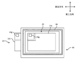
- FIG. 2 is a plan view of an electronic module that can be used in the first embodiment of the present invention.
- FIG. 3A is a longitudinal sectional view of a first connection body that can be used in the first embodiment of the present invention, and FIG. 3B is used in the first embodiment of the present invention. It is a longitudinal cross-sectional view of another possible first connection body.
- FIG. 4A is a longitudinal sectional view of a first contact body that can be used in the second embodiment of the present invention, and FIG. 4B is used in the second embodiment of the present invention. It is a longitudinal cross-sectional view of another 1st contact body which may be obtained.
- FIG. 1 is a longitudinal sectional view of an electronic module that can be used in the first embodiment of the present invention.
- FIG. 2 is a plan view of an electronic module that can be used in the first embodiment of the present invention.
- FIG. 3A is a
- FIG. 5 (a) is a longitudinal sectional view of a first contact body that can be used in the third embodiment of the present invention
- FIG. 5 (b) is a first view shown in FIG. 5 (a).
- It is a top view of a contact body.
- FIG. 6A is a longitudinal sectional view of a second contact body that can be used in the fourth embodiment of the present invention
- FIG. 6B is a second cross-sectional view shown in FIG. It is a bottom view of a contact body.
- FIG. 7A is a longitudinal sectional view of a first contact body that can be used in the fifth embodiment of the present invention
- FIG. 7B is used in the fifth embodiment of the present invention. It is a longitudinal cross-sectional view of another 1st contact body which can be obtained FIG.
- FIG. 8 is a longitudinal sectional view of a second contact body that can be used in the sixth embodiment of the present invention.
- FIG. 9A is a longitudinal sectional view of a first contact body that can be used in the seventh embodiment of the present invention, and FIG. 9B is used in the seventh embodiment of the present invention. It is a longitudinal cross-sectional view of another 1st contact body which can be obtained
- FIG. 10 is a plan view of an electronic module that can be used in the eighth embodiment of the present invention.
- FIG. 11 is a longitudinal sectional view of an electronic module that can be used in the ninth embodiment of the present invention.
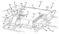
- FIG. 12 is a perspective view of an electronic module that can be used in the tenth embodiment of the present invention.
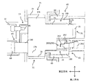
- FIG. 13 is a plan view of an electronic module that can be used in the tenth embodiment of the present invention.
- FIG. 14 is a side view of an electronic module that can be used in the tenth embodiment of the present invention.
- first direction the left and right direction
- second direction the front and back direction of the paper surface
- third direction An in-plane direction including the second direction and the third direction
- plane direction when viewed from above in FIG.
- the electronic module of the present embodiment may have a first electronic unit and a second electronic unit.
- the first electronic unit is provided on a first substrate 11, a plurality of first conductor layers 12 provided on one side of the first substrate 11, and one side of the first conductor layer 12.
- the first electronic element 13 may be included.
- the first electronic element 13 may be a switching element or a control element.
- the first electronic element 13 may be a MOSFET, an IGBT, or the like.
- Each of the first electronic element 13 and the second electronic element 23 described later may be composed of a semiconductor element, and the semiconductor material may be silicon, silicon carbide, gallium nitride, or the like.
- the other surface of the first electronic element 13 may be connected to the first conductor layer 12 via a conductive adhesive 5 such as solder (see FIG. 4 and the like).
- the conductive adhesive 5 is not shown in FIGS.
- the first connection body 60 may be provided on one side of the first electronic element 13.
- the first connection body 60 may be connected to one surface of the first electronic element 13 via a conductive adhesive 5 such as solder.
- a second electronic unit may be provided on one side of the first connection body 60.
- the second electronic unit may have a second electronic element 23 provided on one side of the first connection body 60.
- the second electronic unit may include a second substrate 21 and a second conductor layer 22 provided on the other side of the second substrate 21.
- a second connection body 70 may be provided on the other side of the second conductor layer 22.
- the second electronic element 23 may be provided on the second conductor layer 22, unlike the embodiment shown in FIG. 1.
- the second connection body 70 may be connected to one surface of the second electronic element 23 and the other surface of the second conductor layer 22 via a conductive adhesive such as solder.
- the second electronic element 23 may be a switching element or a control element.
- the second electronic element 23 may be a MOSFET, an IGBT, or the like.
- the first connection body 60 may include a first head portion 61 and a first column portion 62 extending from the first head portion 61 to the other side.
- the second connector 70 may include a second head portion 71 and a second column portion 72 extending from the second head portion 71 to the other side.
- the first connection body 60 may have a substantially T-shaped cross section, and the second connection body 70 may have a substantially T-shaped cross section.
- An abutment body 250 that abuts on one surface of the second electronic element 23 and can apply a force toward the one side to the second substrate 21 may be provided.
- contact in the present application includes not only direct contact but also indirect contact. As an aspect which contact
- the contact body 250 has a first contact body 260 in the present embodiment.
- the first contact body 260 extends from the second substrate side contact portion 262 to the second conductor side 22 or the second substrate 21, and extends from the second substrate side contact portion 262 to the other side. Or you may have the 1st board
- the first contact body 260 includes a contact base end portion 263 that contacts one surface of the second electronic element 23 and a direction inclined from the contact base end portion 263 with respect to the surface direction.
- the second substrate side contact portion 262 that extends to one side and contacts the second conductor layer 22 or the second substrate 21 and the second substrate side contact portion 262 on the other side in a direction inclined with respect to the surface direction.
- the contact proximal end portion 263 may be connected to a terminal (for example, a second gate terminal 23g described later) of the second electronic element 23 via the conductive adhesive 5 or the like.
- the second substrate side contact portion 262 may contact the second conductor layer 22, and the first substrate side contact portion 261 may contact the first conductor layer 12.
- the second conductor layer 22 in contact with the second substrate side contact portion 262 is electrically connected to the other second conductor layer 22, the first conductor layer 12, the first electronic element 13, and the second electronic element 23. It does not have to fulfill its electrical function.
- the electronic module includes a first electronic element 13, a second electronic element 23, a first connection body 60, a second connection body 70, a first contact body 260, a connector 85 (see FIG. 13) described later, and a first conductor layer. 12 and the sealing part 90 comprised from the sealing resin etc. which seal the 2nd conductor layer 22 (refer FIG. 1).
- the first conductor layer 12 in contact with the first substrate side contact portion 261 may protrude outward from the sealing portion 90 and be connected to the terminal portion 110 that can be connected to an external device.
- a first groove portion 64 may be provided on one surface of the first head portion 61.
- the first groove portion 64 is provided on the outer periphery of the first column portion 62 in plan view (surface direction), but may be provided on a part of the outer periphery of the first column portion 62. It may be provided all around the periphery.
- a conductive adhesive 5 such as solder may be provided on one side of the first head portion 61 and on the inner periphery of the first groove portion, and the second electronic element is interposed via the conductive adhesive 5. 23 may be provided.
- the cross section of the first groove portion 64 may be rectangular as shown in FIG. 3B, or may be triangular as shown in FIG.
- the triangle shape may be a right triangle or an isosceles triangle.
- the first electronic element 13 may be exposed outward from the first head portion 61 in plan view.
- the first electronic element 13 is a switching element such as a MOSFET
- the first gate terminal 13g and the like may be provided in a portion exposed from the outside.
- the second electronic element 23 is a switching element such as a MOSFET
- a second gate terminal 23g or the like may be provided on one surface.
- the first electronic element 13 shown in FIG. 2 has a first gate terminal 13g and a first source terminal 13s on one side
- the second electronic element 23 has a second gate terminal 23g and a first source terminal 13s on one side. Two source terminals 23s are provided.
- the second connection body 70 is connected to the second source terminal 23s of the second electronic element 23 via a conductive adhesive
- the first contact body 260 is connected to the second gate terminal 23g of the second electronic element 23. It may be connected via a conductive adhesive.
- the 1st connection body 60 may connect the 1st source terminal 13s of the 1st electronic element 13, and the 2nd drain terminal provided in the other side of the 2nd electronic element 23 via a conductive adhesive.
- the first drain terminal provided on the other side of the first electronic element 13 may be connected to the first conductor layer 12 via a conductive adhesive.
- the first gate terminal 13g of the first electronic element 13 is connected to a connector 85 (see FIG. 13) via a conductive adhesive, and the connector 85 is connected to the first conductor layer 12 via a conductive adhesive. May be.
- the second electronic element 23 placed on the first connection body 60 is a control element having low heat generation
- the electronic element 13 may be a switching element
- the first electronic element 13 may be a control element having low heat generation
- first electronic element 13, the second electronic element 23, the first connection body 60, the second connection body 70, the first contact body 260, and the connector 85 may constitute a chip module.
- the chip module having the first electronic element 13, the second electronic element 23, the first connection body 60, the second connection body 70, the first contact body 260 and the connector 85 is connected to the first conductor layer 12.
- An electronic module may be manufactured by sealing between the first substrate 11 having the second substrate 21 and the second substrate 21 having the second conductor layer 22 and then sealing with the sealing portion 90.
- the first substrate 11 and the second substrate 21 a ceramic substrate, an insulating resin layer, or the like can be adopted.
- a material mainly composed of Ag or Cu can be used.
- a metal such as Cu can be used.
- the joining of the terminal part 110 and the conductor layers 12 and 22 is not limited to a mode in which the conductive adhesive 5 such as solder is used, but laser welding or ultrasonic bonding may be used. Good.
- the first contact body 170 does not need to adopt an electrically meaningful aspect, and the second conductor layer 22 with which the first contact member 172 contacts is the other second conductor layer 22, the first conductor layer 12, It is also possible to adopt a mode in which the first electronic element 13 and the second electronic element 23 are not electrically connected and do not perform an electrical function.
- the second substrate 21 is disposed on the other side. Can be prevented.
- the contact body 250 as in the present embodiment, it is possible to prevent such a problem from occurring. Such an effect is also exhibited in the contact body 250 in other embodiments described later.
- a contact base end portion 263 that contacts one surface of the second electronic element 23, and extends from the contact base end portion 263 to one side, and the second conductor layer 22 or the second substrate 21.
- a second substrate side contact portion 262 that contacts the first conductor layer 12 or the first substrate 11 and extends from the second substrate side contact portion 262 to the other side.
- the second substrate side contact portion 262 is provided between the contact base end portion 263 and the first substrate side contact portion 261 in the surface direction, the second substrate side contact portion 262 is provided. This is advantageous in that a force can be applied to one side while the portion 262 is supported by both the contact base end portion 263 and the first substrate side contact portion 261.
- the contact base end portion 263 contacts the second electronic element 23 via the conductive adhesive 5 or the like, and the second substrate side contact portion 262 contacts the second conductor layer 22 via the conductive adhesive 5 or the like.
- the position of the first contact body 260 by the conductive adhesive 5 is adopted. Can be prevented from shifting.
- a force is applied to the first substrate 11 and the second substrate 21 to be warped or distorted by the application of heat, but the position of the first contact body 260 can be prevented from shifting at this time. It is beneficial.
- the second conductor layer 22 that contacts the second substrate side contact portion 262 is electrically connected to the other second conductor layer 22, the first conductor layer 12, the first electronic element 13, and the second electronic element 23.
- the second substrate side contact portion 262 of the first contact body 260 is inadvertently conducted, and the first electron exhibits an unexpected behavior. This is advantageous in that the device 13 and the second electronic device 23 can be prevented from showing.
- the first contact body 260 can also be used as a connector for connecting the second electronic element 23 and the terminal portion 110, and without increasing the number of components, the first substrate 11 and the second substrate. This is advantageous in that the substrate 21 can be prevented from being warped or distorted.
- the second substrate side contact portion 262 is provided with a first convex portion 265 projecting to one side, and the second substrate side contact portion 262 is electrically conductive.
- the second conductor layer 22 is brought into contact with the adhesive 5 through the adhesive 5.
- the conductive adhesive 5 can have a sufficient thickness, and cracks and the like can be prevented from entering the conductive adhesive 5. Since the first contact body 260 presses the second substrate 21 toward one side, it is difficult to provide a gap between the second substrate side contact portion 262 and the second conductor layer 22. It has become.
- substrate side contact part 262 by providing the 1st convex part 265 like this point and this point is employ
- the first convex portion 265 may have a hemispherical or arcuate cross section as shown in FIG. 4 (a), or may have a trapezoidal cross section as shown in FIG. 4 (b). Moreover, it is not restricted to these, The vertical cross section of the 1st convex part 265 may be rectangular shape, and may be triangular shape.
- At least a part of the first convex portion 265 may be in contact with the second conductor layer 22, or as shown in FIG. 4B, the first convex portion 265. May not contact the second conductor layer 22.
- one or more legs 266 (266a, 266b) extending to the other side are provided, and the legs 266 contact the first conductor layer 12 or the first substrate 11. It is a form to touch.
- a description will be given using an aspect in which two leg portions 266 extending from the second substrate side contact portion 262, more specifically, a first leg portion 266a and a second leg portion 266b are provided.
- Only one leg 266 may be provided, or three or more legs 266 may be provided.
- all the aspects demonstrated by said each embodiment are employable.
- the members described in the above embodiments will be described using the same reference numerals.
- the leg portion 266 can apply a force toward one side to the second substrate 21 while receiving support from the first substrate 11 side. It is beneficial.
- the pair of leg portions 266 extends from both sides of the second substrate side abutting portion 262.
- the first substrate is used. This is advantageous in that a force directed to one side can be applied to the second substrate 21 while receiving support from the 11 side in a well-balanced manner.
- the leg portion 266 does not need to extend from the second substrate side contact portion 262.
- the leg portion 266 may extend from the first substrate side contact portion 261.
- the second substrate side contact portion 262 is replaced with the contact base end portion 263, the first substrate side contact portion 261, and the pair of leg portions. 266 can be supported from four directions, and is advantageous in that a force directed to one side can be applied to the second substrate 21 while receiving support from the first substrate 11 side in a more balanced manner.
- first conductor layer 12 in contact with the leg 266 is not electrically connected to the other second conductor layer 22, the first conductor layer 12, the first electronic element 13, and the second electronic element 23.
- first electronic element 13 and the second electronic element 23 can be prevented from exhibiting unexpected behavior due to conduction of the leg 266.
- the area of the leg contact portion 267 (267a, 267b) where the leg portion 266 contacts the first conductor layer 12 or the first substrate 11 is such that the first substrate side contact portion 261 is the first conductor layer 12 or the first substrate 11. It may be smaller than the area in contact with.
- a space for providing the leg portion 266 or the first conductor layer 12 on which the leg portion 266 is provided on the first substrate 11 is necessary.
- substrate 11 is 1st board
- the portion 261 may be larger than the area in contact with the first conductor layer 12 or the first substrate 11. Further, among the plurality of leg portions 266, the area of the leg contact portion 267 that contacts the first conductor layer 12 or the first substrate 11 of some of the leg portions 266 is such that the first substrate-side contact portion 261 is the first. The area of the leg contact portion 267 that contacts the first conductor layer 12 or the first substrate 11 of the remaining leg portion 266 is larger than the area that contacts the conductor layer 12 or the first substrate 11.
- the contact portion 261 may be smaller than the area in contact with the first conductor layer 12 or the first substrate 11. Further, the area of the leg contact portion 267 where the leg portion 266 contacts the first conductor layer 12 or the first substrate 11 is such that the first substrate side contact portion 261 contacts the first conductor layer 12 or the first substrate 11. It may be the same size as the area.
- the first contact body 260 has been described.
- a description will be given using a mode in which the second contact body 270 is employed.
- the second contact body 270 includes a first contact member 271 that contacts one surface of the second electronic element 23 and a first contact member 271 provided on one side of the first contact member 271.
- the two abutting members 272, the first abutting member 271 and the second abutting member 272 are coupled, and the second abutting member 272 has a coupling member 273 that can apply a force toward one side.
- the members described in the above embodiments will be described using the same reference numerals.
- the second abutment body 270 As in the present embodiment is employed, the second abutment is performed by the urging force of the connecting member 273 while receiving support from the second electronic element 23 and the first abutment member 271.
- the member 272 can apply a force toward one side to the second substrate 21, and can prevent the second substrate 21 from being bent to the other side.
- the first contact member 271 may contact one surface of the second electronic element 23 via the conductive adhesive 5 or the like.
- the second contact member 272 may contact the second conductor layer 22 via the conductive adhesive 5 or the like.
- it can prevent that the position of the 2nd contact body 270 shifts
- a force is applied to cause the first substrate 11 and the second substrate 21 to be warped or distorted by the application of heat.
- the position of the second contact body 270 can be prevented from shifting at this time. It is beneficial.
- the second contact body 270 may be provided instead of the first contact body 260.
- the second electronic element 23 is a switching element such as a MOSFET and the second gate terminal 23g is provided
- the first contact member 271 of the second contact body 270 is electrically conductive to the second gate terminal 23g.
- the second conductor layer 22 connected via the adhesive 5 and connected to the second contact body 270 may be connected to the terminal portion 110.
- the second contact body 270 can be used as a connection body for connecting the second electronic element 23 and the terminal portion 110, and without increasing the number of parts, This is advantageous in that the substrate 11 and the second substrate 21 can be prevented from being warped or distorted.
- the second contact member 272 covers the periphery of the second gate terminal 23 g on the bottom surface (the other surface), and the conductive adhesive 5 such as solder provided on the second gate terminal 23 g.
- You may have the contact recessed part 274 for covering.
- Employing such a contact recess 274 is advantageous in that the second contact body 270 can be positioned with respect to the second gate terminal 23g. If such positioning is taken into consideration, the size of the contact recess 274 in the surface direction may be slightly larger (for example, 1 to 3 mm) than the second gate terminal 23g.
- the second contact body 270 it is not necessary for the second contact body 270 to adopt an electrically meaningful mode, and the second conductor layer 22 with which the second contact member 272 contacts is the other second conductor layer 22 and the first conductor. It is also possible to adopt a mode in which the layer 12, the first electronic element 13, and the second electronic element 23 are not electrically connected and do not perform an electrical function.
- FIG. 7A a mode in which a projecting body 275 projecting to one side is provided on one side surface of the first abutting member 271, or FIG.
- the second contact member 272 is provided with a protrusion 275 that protrudes on the other side of the surface.
- Other configurations are the same as those in the fourth embodiment.
- all the aspects demonstrated by said each embodiment are employable.
- the members described in the above embodiments will be described using the same reference numerals.
- the protrusions 275 may be provided on each of the one surface of the first contact member 271 and the other surface of the second contact member 272.
- the projecting body 275 As in the present embodiment, even if the warp and distortion of the first substrate 11 and the second substrate 21 increase, the first substrate 11 and the second substrate 21 warp beyond a certain value. Or warping. That is, by providing the projecting body 275 as in the present embodiment, the second contact member 272 contacts the projecting body 275 even if the warpage and distortion of the first substrate 11 and the second substrate 21 increase. Further, it is advantageous in that the first substrate 11 or the second substrate 21 can be prevented from being warped or distorted.
- the projecting body 275 may have a projecting recess 275a at the center.
- a projecting recess 275a is provided, when an excessive force is applied, the projecting portion 275 can be recessed toward the projecting recess 275a, and the second substrate 21 or the like is damaged by the excessive force. This is beneficial in that it can be prevented.
- the second contact member 272 may be inclined to one side with respect to the surface direction.
- Other configurations are the same as those of the fifth embodiment.
- All the aspects demonstrated by said each embodiment are employable.
- the members described in the above embodiments will be described using the same reference numerals.
- the second substrate 21 can be pressed more strongly by the second contact member 272. It is beneficial in that it can be done.
- substrate 21 will be pressed from one side by a metal mold
- the second abutment member 272 is provided with a second convex portion 279 that protrudes to one side.
- Other configurations are the same as those of the fifth embodiment.
- all aspects described in the above embodiments can be adopted.
- the members described in the above embodiments will be described using the same reference numerals.
- the agent 5 can be given a sufficient thickness, and cracks and the like can be prevented from entering the conductive adhesive 5. Since the second contact body 270 presses the second substrate 21 toward one side, it is difficult to provide a gap between the second contact member 272 and the second conductor layer 22. Yes. In this regard, even when the conductive adhesive 5 is provided between the second conductor layer 22 and the second contact member 272, the second convex portion 279 as in the present embodiment is provided. Thereby, it can prevent that the conductive adhesive 5 cracks.
- the second convex portion 279 may have a hemispherical or arcuate cross section as shown in FIG. 9A, or may have a trapezoidal cross section as shown in FIG. 9B. Moreover, it is not restricted to these, The vertical cross section of the 2nd convex part 279 may be a rectangular shape, and may be a triangular shape.
- the 1st contact body 260 and the 2nd contact body 270 can also be employ
- first contact body 260 and the second contact body 270 When both the first contact body 260 and the second contact body 270 are employed, one of the first contact body 260 and the second contact body 270 is connected to a terminal such as the second gate terminal 23g. The other is not connected to a terminal such as the second gate terminal 23g and may not have an electrical function.
- the contact base end portion 263 of the first contact body 260 has a terminal or the like on one surface of the second electronic element 23.
- the first contact member 271 of the second contact body 270 may be provided in the second electronic element 23 when the second contact body 270 does not have a function as a terminal. It may be provided at a location where no terminal or the like is provided on one of the surfaces.
- both the 1st contact body 260 and the 2nd contact body 270 are not connected to terminals, such as the 2nd gate terminal 23g, and do not need to have an electrical function.
- the first connection body 60 having a substantially T-shaped cross section is used.
- the first connection body 60 of the present embodiment has a first head portion 61 as shown in FIG.
- the support body 65 comes into contact with the first conductor layer or the first substrate.
- all the aspects demonstrated by said each embodiment are employable.
- the members described in the above embodiments will be described using the same reference numerals.
- the second electronic element is mounted when the second electronic element 23 is mounted or after the second electronic element 23 is mounted. It is possible to prevent the first connecting body 60 from being inclined by the weight of 23. Moreover, heat dissipation can be improved because the support part 65 contacts the 1st board
- the some support part 65 is provided like this Embodiment, it is beneficial at the point which can provide the 1st connection body 60 more stably and can implement
- Each of the support portions 65 may have support base end portions 69 (69a to 69d) that extend in the surface direction and come into contact with the first substrate 11 or the first conductor layer 12. Further, it is not necessary to provide the support base end portion 69 in each of the plurality of support portions 65, the support base end portion 69 is provided in a part of the plurality of support portions 65, and the support base end portion 69 is provided in the remaining portion. It may not be provided.
- the first connection body 60 can be arranged on the first substrate 11 or the first conductor layer 12 in a more balanced manner. Since the contact area with the 1st board
- Each of the support parts 65 may contact the first conductor layer 12.
- the first conductor layer 12 connected to the support portion 65 is not electrically connected to the other first conductor layer 12, second conductor layer 22, first electronic element 13, and second electronic element 23.
- Each of the support portions 65 extends in the height direction (first direction) from the end portion of the surface direction support portion 166 and the surface direction support portion 166 (166a-166d) extending in the surface direction from the first head portion 61. It may have a height direction support portion 165 (165a-165d) (see also a sixth embodiment described later).
- the surface direction support portion 166 means a portion having a length in the width direction shorter than that of the first head portion 61.
- the support part 65 does not have the surface direction support part 166 but may have only the height direction support part 165 extending in the height direction (first direction) from the first head part 61.
- the contact body 250 described in each of the above embodiments it is beneficial to use the support portion 65 as in the present embodiment.
- the contact body 250 is provided on one surface of the second electronic element 23 directly or indirectly through the conductive adhesive 5 or the like, but the second electronic element 23 is disposed in a stable state. Otherwise, when the second substrate 21 is pressed against the one side by the contact body 250, the second electronic element 23 may be inclined.
- the first connection body 60 has the support portion 65, even if the second electronic element 23 is pressed against the other side by the contact body 250, The electronic element 23 can be prevented from tilting. As a result, the second substrate 21 can be stably pressed to one side by the contact body 250.
- the abutting base end 263 abuts on one surface of the second electronic element 23, but the first substrate 11 and the second substrate 21 are heated by the application of heat. A force is applied to the second electronic element 23 via the abutting base end portion 263 when the warp or distortion is attempted.
- the first connection body 60 has the support portion 65, the second electronic element 23 can be prevented from being tilted, and as a result, the second substrate 21 is disposed on the first substrate side.
- the contact portion 261 can be stably pressed to one side.
- the first contact member 271 contacts the one surface of the second electronic element 23.
- the first substrate 11 and the second substrate 21 are heated by the application of heat.
- a force is applied to the second electronic element 23 via the first contact member 271 when attempting to warp or distort.
- the second electronic element 23 can be prevented from being inclined, and as a result, the second substrate 21 is brought into the second contact.
- the member 272 can be stably pressed to one side.
- the second connecting body 70 having the second pillar portion 72 having a substantially T-shaped cross section has been described.
- the present embodiment as shown in FIG. 70 has an extending portion 75 (75a, 75b) extending from the second head portion 71 to the other side.
- extending portion 75 75a, 75b
- all the aspects demonstrated by each embodiment mentioned above are employable.
- the members described in the above embodiments will be described using the same reference numerals.
- the extending portion 75 since the extending portion 75 is provided, heat from the second electronic element 23 can be efficiently radiated, and a high heat radiating effect can also be realized by the second connection body 70. . Moreover, when the some extension part 75 is provided like this Embodiment, it is beneficial at the point which can implement
- Each of the extended portions 75 may abut on the first conductor layer 12.
- the first conductor layer 12 connected to the extending portion 75 may not be electrically connected to the other first conductor layer 12 and the first electronic element 13.
- Each of the extended portions 75 may have extended base end portions 79 (79a, 79b) that extend in the surface direction and come into contact with the first substrate 11 or the first conductor layer 12. Further, it is not necessary to provide the extended base end portion 79 in each of the plurality of extending portions 75, and the extended base end portion 79 is provided in a part of the plurality of extending portions 75 and extends to the remaining portion. The base end 79 may not be provided.
- the second connecting body 70 can be arranged on the first substrate 11 or the first conductor layer 12 in a more balanced manner, and the extended proximal end portion Since the contact area with the first substrate 11 or the first conductor layer 12 can be increased by 79, the heat dissipation effect can be enhanced.
- the second connection body 70 having a plurality of extending portions 75 When the second connection body 70 having a plurality of extending portions 75 is employed as in the present embodiment, a repulsive force that pushes back the second substrate 21 to one side can be applied, as with the contact body 250. Become. That is, as described above, a force is applied to the first substrate 11 and the second substrate 21 to be warped or distorted by the application of heat, but by using the second connection body 70 having a plurality of extending portions 75. In addition to the effects of the first contact body 260 and the second contact body 270, the second connection body 70 is also advantageous in that warpage and distortion of the first substrate 11 and the second substrate 21 can be prevented.
- the extending portion 75 of the present embodiment has a height direction extending portion 175 (175a, 175b) extending from the second head portion 71 in the height direction (first direction).
- both the support portion 65 and the extension portion 75 may be employed.
- a mode in which three support portions 65 and three extension portions 75 are used will be described as an example.
- all the aspects demonstrated by each embodiment mentioned above are employable.
- the members described in the above embodiments will be described using the same reference numerals.
- the extending portion 75 includes a surface extending portion 176 extending in the surface direction from the second head portion 71 and a height direction (first direction) extending from the surface extending portion 176. You may have the height direction extension part 175 extended.
- the surface direction extending portion 176 means a portion whose size in the width direction is smaller than that of the second head portion 71.
- the effect of having the contact body 250, the effect of having the plurality of support portions 65, and the effect of having the plurality of extending portions 75 can be obtained. It is beneficial.
Landscapes
- Coupling Device And Connection With Printed Circuit (AREA)
- Structures For Mounting Electric Components On Printed Circuit Boards (AREA)
- Cooling Or The Like Of Semiconductors Or Solid State Devices (AREA)
- Combinations Of Printed Boards (AREA)
Abstract
電子モジュールは、第一基板11と、前記第一基板11の一方側に設けられた第一電子素子13と、前記第一電子素子13の一方側に設けられた第一接続体60と、前記第一接続体60の一方側に設けられた第二電子素子23と、前記第二電子素子23の一方側に設けられた第二基板21と、前記第二電子素子23の一方側の面に当接し、前記第二基板21に対して一方側に向かう力を付与できる当接体250と、を有する。
Description
本発明は、複数の電子素子を有する電子モジュールに関する。
複数の電子素子が封止樹脂内に設けられた電子モジュールが従来から知られている(例えば特開2014-45157号参照)。このような電子モジュールに関して小型化することが望まれている。
小型化する一つの手段として、電子素子を層状に積み重ねていく態様を採用することが考えられる。その際には、電子素子(第一電子素子)の一方側(例えばおもて面側)に別の電子素子(第二電子素子)を設けることが考えられる。
このような態様によれば、電子素子が増える分、配線の引き回しのために第一電子素子側の第一基板と第二電子素子側の第二基板が大きくなることがある。このように第一基板及び第二基板の大きさが大きくなると、ソルダー工程、リフロー工程等の熱処理工程においてこれら第一基板及び第二基板が反ったり歪んだりすることがある。このような反り又は歪みを防止するために、第一基板と第二基板の間に支柱等を設けることも考えられるが、このような態様によれば、部品点数が増えてしまう。
本発明は、第一基板又は第二基板の反りや歪みを部品点数を増やすことなく防止できる電子モジュールを提供する。
本発明による電子モジュールは、
第一基板と、
前記第一基板の一方側に設けられた第一電子素子と、
前記第一電子素子の一方側に設けられた第一接続体と、
前記第一接続体の一方側に設けられた第二電子素子と、
前記第二電子素子の一方側に設けられた第二基板と、
前記第二電子素子の一方側の面に当接し、前記第二基板に対して一方側に向かう力を付与できる当接体と、
を備え、
前記当接体が、前記第二電子素子と外部装置に接続可能な端子部とを電気的に接続してもよい。
第一基板と、
前記第一基板の一方側に設けられた第一電子素子と、
前記第一電子素子の一方側に設けられた第一接続体と、
前記第一接続体の一方側に設けられた第二電子素子と、
前記第二電子素子の一方側に設けられた第二基板と、
前記第二電子素子の一方側の面に当接し、前記第二基板に対して一方側に向かう力を付与できる当接体と、
を備え、
前記当接体が、前記第二電子素子と外部装置に接続可能な端子部とを電気的に接続してもよい。
本発明による電子モジュールは、
前記第一基板と記第一電子素子との間に設けられた第一導体層と、
前記第二基板の他方側に設けられた第二導体層と、をさらに備え、
前記当接体は第一当接体を有し、
前記第一当接体は、前記第二電子素子の一方側の面に当接する当接基端部と、前記当接基端部から一方側に延び、前記第二導体層又は前記第二基板に当接する第二基板側当接部と、前記第二基板側当接部から他方側に延び、前記第一導体層又は前記第一基板に当接する第一基板側当接部とを有してもよい。
前記第一基板と記第一電子素子との間に設けられた第一導体層と、
前記第二基板の他方側に設けられた第二導体層と、をさらに備え、
前記当接体は第一当接体を有し、
前記第一当接体は、前記第二電子素子の一方側の面に当接する当接基端部と、前記当接基端部から一方側に延び、前記第二導体層又は前記第二基板に当接する第二基板側当接部と、前記第二基板側当接部から他方側に延び、前記第一導体層又は前記第一基板に当接する第一基板側当接部とを有してもよい。
本発明による電子モジュールにおいて、
前記第一基板は金属基板からなり、
前記第二基板は金属基板からなり、
前記当接体は第一当接体を有し、
前記第一当接体は、前記第二電子素子の一方側の面に当接する当接基端部と、前記当接基端部から一方側に延び、前記第二基板に当接する第二基板側当接部と、前記第二基板側当接部から他方側に延び、前記第一基板に当接する第一基板側当接部とを有してもよい。
前記第一基板は金属基板からなり、
前記第二基板は金属基板からなり、
前記当接体は第一当接体を有し、
前記第一当接体は、前記第二電子素子の一方側の面に当接する当接基端部と、前記当接基端部から一方側に延び、前記第二基板に当接する第二基板側当接部と、前記第二基板側当接部から他方側に延び、前記第一基板に当接する第一基板側当接部とを有してもよい。
本発明による電子モジュールにおいて、
前記第二基板側当接部は一方側に突出した第一凸部を有し、
前記第二基板側当接部は導電性接着剤を介して前記第二導体層に当接してもよい。
前記第二基板側当接部は一方側に突出した第一凸部を有し、
前記第二基板側当接部は導電性接着剤を介して前記第二導体層に当接してもよい。
本発明による電子モジュールにおいて、
前記第一当接体は、他方側に延びた一つ以上の脚部を有し、
前記脚部は、前記第一導体層又は前記第一基板に当接してもよい。
前記第一当接体は、他方側に延びた一つ以上の脚部を有し、
前記脚部は、前記第一導体層又は前記第一基板に当接してもよい。
本発明による電子モジュールにおいて、
前記脚部が前記第一導体層又は前記第一基板に当接する面積は、前記第一基板側当接部が前記第一導体層又は前記第一基板に当接する面積よりも小さくてもよい。
前記脚部が前記第一導体層又は前記第一基板に当接する面積は、前記第一基板側当接部が前記第一導体層又は前記第一基板に当接する面積よりも小さくてもよい。
本発明による電子モジュールにおいて、
前記当接体は第二当接体を有し、
前記第二当接体は、前記第二電子素子の一方側の面に当接する第一当接部材と、前記第一当接部材の一方側に設けられた第二当接部材と、前記第一当接部材と前記第二当接部材とを連結し、前記第二当接部材に一方側に向かう力を付与できる連結部材とを有してもよい。
前記当接体は第二当接体を有し、
前記第二当接体は、前記第二電子素子の一方側の面に当接する第一当接部材と、前記第一当接部材の一方側に設けられた第二当接部材と、前記第一当接部材と前記第二当接部材とを連結し、前記第二当接部材に一方側に向かう力を付与できる連結部材とを有してもよい。
本発明の一態様として、第二電子素子の一方側の面に当接し、第二基板に対して一方側に向かう力を付与できる当接体であって、第二電子素子と外部装置に接続可能な端子とを電気的に接続する当接体を採用した場合には、第一基板又は第二基板の反りや歪みを部品点数を増やすことなく防止できる。
第1の実施の形態
《構成》
本実施の形態において、「一方側」は図1の上方側を意味し、「他方側」は図1の下方側を意味する。図1の上下方向を「第一方向」と呼び、左右方向を「第二方向」と呼び、紙面の表裏方向を「第三方向」と呼ぶ。第二方向及び第三方向を含む面内方向を「面方向」といい、図1の上方から見た場合には「平面視」という。
《構成》
本実施の形態において、「一方側」は図1の上方側を意味し、「他方側」は図1の下方側を意味する。図1の上下方向を「第一方向」と呼び、左右方向を「第二方向」と呼び、紙面の表裏方向を「第三方向」と呼ぶ。第二方向及び第三方向を含む面内方向を「面方向」といい、図1の上方から見た場合には「平面視」という。
本実施の形態の電子モジュールは、第一電子ユニットと、第二電子ユニットとを有してもよい。
図1に示すように、第一電子ユニットは、第一基板11と、第一基板11の一方側に設けられた複数の第一導体層12と、第一導体層12の一方側に設けられた第一電子素子13と、を有してもよい。第一電子素子13はスイッチング素子であってもよいし、制御素子であってもよい。第一電子素子13がスイッチング素子である場合には、第一電子素子13はMOSFETやIGBT等であってもよい。第一電子素子13及び後述する第二電子素子23の各々は半導体素子から構成されてもよく、半導体材料としてはシリコン、炭化ケイ素、窒化ガリウム等であってもよい。第一電子素子13の他方側の面は第一導体層12とはんだ等の導電性接着剤5(図4等参照)を介して接続されてもよい。なお、表示を簡易化するために、図1、図11等では導電性接着剤5を示していない。
第一電子素子13の一方側には第一接続体60が設けられてもよい。第一接続体60は第一電子素子13の一方側の面とはんだ等の導電性接着剤5を介して接続されてもよい。
図1に示すように、第一接続体60の一方側には第二電子ユニットが設けられてもよい。第二電子ユニットは、第一接続体60の一方側に設けられた第二電子素子23を有してもよい。また、第二電子ユニットは、第二基板21と、第二基板21の他方側に設けられた第二導体層22を有してもよい。第二導体層22の他方側には第二接続体70が設けられてもよい。第二導体層22が設けられている場合には、図1に示す態様とは異なり第二導体層22に第二電子素子23が設けられてもよい。第二接続体70は第二電子素子23の一方側の面及び第二導体層22の他方側の面とはんだ等の導電性接着剤を介して接続されてもよい。
第二電子素子23はスイッチング素子であってもよいし、制御素子であってもよい。第二電子素子23がスイッチング素子である場合には、第二電子素子23はMOSFETやIGBT等であってもよい。
第一接続体60は、第一ヘッド部61と、第一ヘッド部61から他方側に延びた第一柱部62を有してもよい。第二接続体70は、第二ヘッド部71と、第二ヘッド部71から他方側に延びた第二柱部72を有してもよい。第一接続体60は断面が略T字形状となり、第二接続体70も断面が略T字形状となってもよい。
第二電子素子23の一方側の面に当接し、第二基板21に対して一方側に向かう力を付与できる当接体250が設けられてもよい。なお、本願における「当接」には、直接的に当接する態様の他、間接的に当接する態様も含まれている。間接的に当接する態様としては、例えばはんだ等の導電性接着剤5を介して当接される態様を挙げることができる。当接体250は一つだけ設けられてもよいが、複数設けられてもよい。
図1に示すように、本実施の形態では、当接体250が第一当接体260を有している。第一当接体260は、第二導体層22又は第二基板21に当接する第二基板側当接部262と、第二基板側当接部262から他方側に延び、第一導体層12又は第一基板11に当接する第一基板側当接部261とを有してもよい。より具体的には、第一当接体260は、第二電子素子23の一方側の面に当接する当接基端部263と、当接基端部263から面方向に対して傾斜した方向で一方側に延びて第二導体層22又は第二基板21に当接する第二基板側当接部262と、第二基板側当接部262から面方向に対して傾斜した方向で他方側に延びて第一導体層12又は第一基板11に当接する第一基板側当接部261とを有してもよい。当接基端部263は、第二電子素子23の端子(例えば後述する第二ゲート端子23g)と導電性接着剤5等を介して接続されてもよい。
一例として、第二基板側当接部262は第二導体層22に当接し、第一基板側当接部261は第一導体層12に当接してもよい。第二基板側当接部262と当接する第二導体層22は、他の第二導体層22、第一導体層12、第一電子素子13及び第二電子素子23に電気的に接続されておらず、電気的な機能を果たさなくてもよい。
電子モジュールは、第一電子素子13、第二電子素子23、第一接続体60、第二接続体70、第一当接体260、後述する接続子85(図13参照)、第一導体層12及び第二導体層22を封止する封止樹脂等から構成される封止部90を有してもよい(図1参照)。第一基板側当接部261と当接する第一導体層12は、封止部90から外方に突出し、外部装置と接続可能な端子部110に接続されてもよい。
図2に示すように、第一ヘッド部61の一方側の面には第一溝部64が設けられてもよい。第一溝部64は、平面視(面方向)において、第一柱部62の周縁外方に設けられているが、周縁外方の一部に設けられてもよいし、第一柱部62の周縁外方の全部に設けられてもよい。第一ヘッド部61の一方側の面であって、第一溝部の周縁内方にははんだ等の導電性接着剤5が設けられてもよく、導電性接着剤5を介して第二電子素子23が設けられてもよい。第一溝部64の断面は、図3(b)で示すように矩形状であってもよいし、図3(a)で示すように三角形状であってもよい。三角形状としては、直角三角形であってもよいし、二等辺三角形であってもよい。
図2に示すように、平面視において、第一電子素子13は、第一ヘッド部61から外方に露出する態様となってもよい。第一電子素子13がMOSFET等のスイッチング素子である場合には、外方から露出した部分に第一ゲート端子13g等が設けられてもよい。同様に、第二電子素子23がMOSFET等のスイッチング素子である場合には、一方側の面に第二ゲート端子23g等が設けられてもよい。図2に示す第一電子素子13は、一方側の面に第一ゲート端子13gと第一ソース端子13sを有し、第二電子素子23は、一方側の面に第二ゲート端子23gと第二ソース端子23sを有している。この場合、第二接続体70が第二電子素子23の第二ソース端子23sに導電性接着剤を介して接続され、第一当接体260が第二電子素子23の第二ゲート端子23gに導電性接着剤を介して接続されてもよい。また、第一接続体60は第一電子素子13の第一ソース端子13sと第二電子素子23の他方側に設けられた第二ドレイン端子とを導電性接着剤を介して接続してもよい。第一電子素子13の他方側に設けられた第一ドレイン端子は導電性接着剤を介して第一導体層12に接続されてもよい。第一電子素子13の第一ゲート端子13gは導電性接着剤を介して接続子85(図13参照)に接続され、当該接続子85は導電性接着剤を介して第一導体層12に接続されてもよい。
第一電子素子13及び第二電子素子23のいずれか一方だけがスイッチング素子の場合には、第一接続体60に載置される第二電子素子23を発熱性の低い制御素子とし、第一電子素子13をスイッチング素子にすることも考えられる。逆に、第一接続体60に載置される第二電子素子23をスイッチング素子とし、第一電子素子13を発熱性の低い制御素子にすることも考えられる。
また、第一電子素子13、第二電子素子23、第一接続体60、第二接続体70、第一当接体260及び接続子85によってチップモジュールが構成されてもよい。この場合には、第一電子素子13、第二電子素子23、第一接続体60、第二接続体70、第一当接体260及び接続子85を有するチップモジュールを、第一導体層12を有する第一基板11及び第二導体層22を有する第二基板21の間に配置した後で封止部90によって封止することで、電子モジュールが製造されてもよい。
第一基板11及び第二基板21としては、セラミック基板、絶縁樹脂層等を採用することができる。導電性接着剤5としては、はんだの他、AgやCuを主成分とする材料を用いることもできる。第一接続体60及び第二接続体70の材料としてはCu等の金属を用いることができる。なお、基板11,21としては例えば回路パターニングを施した金属基板を用いることもでき、この場合には、基板11,21が導体層12,22を兼ねることになる。
なお、端子部110と導体層12,22との接合は、はんだ等の導電性接着剤5を利用する態様だけではなく、レーザ溶接を利用してもよいし、超音波接合を利用してもよい。
第一当接体170は電気的に意味のある態様を採用する必要はなく、第一当接部材172が当接する第二導体層22が他の第二導体層22、第一導体層12、第一電子素子13及び第二電子素子23に電気的に接続されておらず、電気的な機能を果たさない態様を採用することもできる。
《作用・効果》
次に、上述した構成からなる本実施の形態による作用・効果の一例について説明する。なお、「作用・効果」で説明するあらゆる態様を、上記構成で採用することができる。
次に、上述した構成からなる本実施の形態による作用・効果の一例について説明する。なお、「作用・効果」で説明するあらゆる態様を、上記構成で採用することができる。
第二電子素子23の一方側の面に当接し、第二基板21に対して一方側に向かう力を付与できる当接体250が設けられる態様を採用することで、第二基板21が他方側に撓むことを防止できる。特にチップモジュールが多数配置され、第一基板11及び第二基板21の面方向が大きくなる場合には、熱が加わることで、これら第一基板11及び第二基板21が反ってしまったり歪んでしまったりする可能性がある。この点、本実施の形態のような当接体250を設けることで、このような問題が生じることを防止できる。なお、このような効果は、後述する他の実施の形態における当接体250においても発揮されるものである。
図1に示すように、第二電子素子23の一方側の面に当接する当接基端部263と、当接基端部263から一方側に延び、第二導体層22又は第二基板21に当接する第二基板側当接部262と、第二基板側当接部262から他方側に延び、第一導体層12又は第一基板11に当接する第一基板側当接部261とを有する第一当接体260を用いた場合には、当接基端部263と第一基板側当接部261によって、第一基板11側からの支えを受けつつ、第二基板21に対して一方側に向かう力を付与できる点で有益である。
この態様によれば、面方向において、当接基端部263と第一基板側当接部261の間に第二基板側当接部262が設けられていることから、第二基板側当接部262を当接基端部263と第一基板側当接部261の両方で支えつつ、一方側に力を付与できる点で有益である。
当接基端部263が導電性接着剤5等を介して第二電子素子23に当接し、第二基板側当接部262が導電性接着剤5等を介して第二導体層22に当接し、第一基板側当接部261が導電性接着剤5等を介して第一導体層12に当接する態様を採用した場合には、導電性接着剤5によって第一当接体260の位置がずれてしまうことを防止できる。特に、熱が加わることで第一基板11及び第二基板21が反ったり歪んだりしようとする力が加わるが、この際に第一当接体260の位置がずれてしまうことを防止できる点で有益である。
また、第二基板側当接部262と当接する第二導体層22が他の第二導体層22、第一導体層12、第一電子素子13及び第二電子素子23に電気的に接続されておらず、電気的な機能を果たさない態様を採用した場合には、第一当接体260の第二基板側当接部262が誤って導通して、予想していない挙動を第一電子素子13及び第二電子素子23が示すことを防止できる点で有益である。
第一当接体260が、第二電子素子23の端子(例えば第二ゲート端子23g)と外部装置に接続可能な端子部110とを電気的に接続し、接続子としての機能を果たす態様を採用した場合には、第一当接体260を第二電子素子23と端子部110とを接続する接続子としても利用することができ、部品点数を増やすことなく、第一基板11及び第二基板21が反ってしまったり歪んでしまったりすることを防止できる点で有益である。
第2の実施の形態
次に、本発明の第2の実施の形態について説明する。
次に、本発明の第2の実施の形態について説明する。
本実施の形態では、図4に示すように、第二基板側当接部262に一方側に突出した第一凸部265が設けられており、かつ第二基板側当接部262は導電性接着剤5を介して第二導体層22と当接する態様となっている。その他の構成については、第1の実施の形態と同様であり、第1の実施の形態で説明したあらゆる態様を採用することができる。第1の実施の形態で説明した部材については同じ符号を用いて説明する。
本実施の形態のように、第二基板側当接部262に第一凸部265が設けられた場合には、第二導体層22と第二基板側当接部262との間に設けられた導電性接着剤5に対して十分な厚みを持たせることでき、導電性接着剤5にクラック等が入ることを防止できる。第一当接体260は、第二基板21を一方側に向かって押し付けるものであることから、第二基板側当接部262と第二導体層22との間に間隙が設けられ難い構成となっている。この点、本実施の形態のような第一凸部265を設けることで、第二導体層22と第二基板側当接部262との間に導電性接着剤5を設ける態様を採用した場合であっても、導電性接着剤5にクラックが入ることを防止できる。
第一凸部265は、図4(a)に示すように縦断面が半球又は円弧状になってもよいし、図4(b)に示すように縦断面が台形状になってもよい。また、これらに限られず、第一凸部265の縦断面は長方形状となってもよいし三角形状となってもよい。
また、図4(a)に示すように、第一凸部265の少なくとも一部は第二導体層22と当接してもよいし、図4(b)に示すように、第一凸部265は第二導体層22と当接しなくてもよい。
第3の実施の形態
次に、本発明の第3の実施の形態について説明する。
次に、本発明の第3の実施の形態について説明する。
本実施の形態では、図5に示すように、他方側に延びた一つ以上の脚部266(266a,266b)が設けられ、脚部266が第一導体層12又は第一基板11に当接する態様となっている。本実施の形態では、一例として、第二基板側当接部262から延びる2つの脚部266、より具体的には第一脚部266a及び第二脚部266bが設けられる態様を用いて説明するが、これに限られることはない。脚部266は1つだけであってもよいし、3つ以上設けられてもよい。その他の構成については、上記各実施の形態で説明したあらゆる態様を採用することができる。上記各実施の形態で説明した部材については同じ符号を用いて説明する。
本実施の形態のような脚部266を採用することで、脚部266によって、第一基板11側からの支えを受けつつ、第二基板21に対して一方側に向かう力を付与できる点で有益である。
図5に示す態様では、一対の脚部266が第二基板側当接部262の両側方から延びる態様となっているが、このような一対の脚部266を採用することで、第一基板11側からの支えをバランスよく受けつつ、第二基板21に対して一方側に向かう力を付与できる点で有益である。なお、脚部266は第二基板側当接部262から延びている必要はなく、例えば脚部266は第一基板側当接部261から延びてもよい。
特に図5(b)に示すように、当接基端部263、第二基板側当接部262及び第一基板側当接部261が延在する方向(第二方向)と直交する方向(第三方向)に一対の脚部266が延びる態様を採用した場合には、第二基板側当接部262を、当接基端部263、第一基板側当接部261及び一対の脚部266の四方向から支持することができ、第一基板11側からの支えをよりバランスよく受けつつ、第二基板21に対して一方側に向かう力を付与できる点で有益である。
また、脚部266と当接する第一導体層12が他の第二導体層22、第一導体層12、第一電子素子13及び第二電子素子23に電気的に接続されておらず、電気的な機能を果たさない態様を採用した場合には、脚部266が導通して予想していない挙動を第一電子素子13及び第二電子素子23が示すことを防止できる点で有益である。
脚部266が第一導体層12又は第一基板11に当接する脚当接部267(267a,267b)の面積は、第一基板側当接部261が第一導体層12又は第一基板11に当接する面積よりも小さくなっていてもよい。本実施の形態のような脚部266を設ける場合には、第一基板11に脚部266又は脚部266が設けられる第一導体層12を設けるためのスペースが必要になるが、この態様を採用することで、脚部266が第一導体層12又は第一基板11に当接する面積を小さくできる点で有益である。
なお、このような態様に限られることはなく、脚部266が第一導体層12又は第一基板11に当接する脚当接部267(267a,267b)の面積は、第一基板側当接部261が第一導体層12又は第一基板11に当接する面積よりも大きくなっていてもよい。また、複数の脚部266のうち、一部の脚部266の第一導体層12又は第一基板11に当接する脚当接部267の面積は、第一基板側当接部261が第一導体層12又は第一基板11に当接する面積よりも大きくなり、残部の脚部266の第一導体層12又は第一基板11に当接する脚当接部267の面積は、第一基板側当接部261が第一導体層12又は第一基板11に当接する面積よりも小さくなってもよい。また、脚部266が第一導体層12又は第一基板11に当接する脚当接部267の面積は、第一基板側当接部261が第一導体層12又は第一基板11に当接する面積と同じ大きさであってもよい。
第4の実施の形態
次に、本発明の第4の実施の形態について説明する。
次に、本発明の第4の実施の形態について説明する。
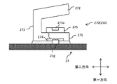
上記各実施の形態では、第一当接体260を用いて説明した。本実施の形態では、第二当接体270が採用された態様を用いて説明する。第二当接体270は、図6に示すように、第二電子素子23の一方側の面に当接する第一当接部材271と、第一当接部材271の一方側に設けられた第二当接部材272と、第一当接部材271と第二当接部材272とを連結し、第二当接部材272に一方側に向かう力を付与できる連結部材273とを有している。その他の構成については、上記各実施の形態で説明したあらゆる態様を採用することができる。上記各実施の形態で説明した部材については同じ符号を用いて説明する。
本実施の形態のような第二当接体270を採用した場合には、第二電子素子23及び第一当接部材271からの支えを受けつつ、連結部材273による付勢力で第二当接部材272によって第二基板21に対して一方側に向かう力を付与でき、第二基板21が他方側に撓むことを防止できる。
第一当接部材271は導電性接着剤5等を介して第二電子素子23の一方側の面に当接してもよい。第二当接部材272は導電性接着剤5等を介して第二導体層22に当接してもよい。このような態様を採用した場合には、導電性接着剤5によって第二当接体270の位置がずれてしまうことを防止できる。特に、熱が加わることで第一基板11及び第二基板21が反ったり歪んだりしようとする力が加わるが、この際に第二当接体270の位置がずれてしまうことを防止できる点で有益である。
第二当接体270は、第一当接体260の代わりに設けられてもよい。第二電子素子23がMOSFET等のスイッチング素子であり、第二ゲート端子23gが設けられている場合には、第二当接体270の第一当接部材271が第二ゲート端子23gに導電性接着剤5を介して接続され、第二当接体270が接続された第二導体層22が端子部110に接続されるようにしてもよい。このような態様を採用した場合には、第二当接体270を第二電子素子23と端子部110とを接続する接続体としても利用することができ、部品点数を増やすことなく、第一基板11及び第二基板21が反ってしまったり歪んでしまったりすることを防止できる点で有益である。
図6に示すように、第二当接部材272は底面(他方側の面)において、第二ゲート端子23gの周縁を覆い、第二ゲート端子23gに設けられるはんだ等の導電性接着剤5を覆うための当接凹部274を有してもよい。このような当接凹部274を採用した場合には、第二ゲート端子23gに対して第二当接体270を位置決めすることができる点で有益である。このような位置決めを考慮するのであれば、当接凹部274の面方向での大きさは第二ゲート端子23gよりもわずかに(例えば1~3mm)大きくなっている態様となってもよい。
このように第二当接体270が電気的に意味のある態様を採用する必要はなく、第二当接部材272が当接する第二導体層22が他の第二導体層22、第一導体層12、第一電子素子13及び第二電子素子23に電気的に接続されておらず、電気的な機能を果たさない態様を採用することもできる。
第5の実施の形態
次に、本発明の第5の実施の形態について説明する。
次に、本発明の第5の実施の形態について説明する。
本実施の形態では、図7(a)に示すように、第一当接部材271の一方側の面に一方側に突出した突出体275が設けられている態様、又は、図7(b)に示すように、第二当接部材272の他方側の面に他方側に突出した突出体275が設けられる態様となっている。その他の構成については、第4の実施の形態と同様である。その他の構成については、上記各実施の形態で説明したあらゆる態様を採用することができる。上記各実施の形態で説明した部材については同じ符号を用いて説明する。なお、第一当接部材271の一方側の面と第二当接部材272の他方側の面の各々に突出体275が設けられてもよい。
本実施の形態のような突出体275が設けられることで、第一基板11及び第二基板21の反りや歪みが大きくなっても、一定値以上は第一基板11及び第二基板21が反ったり歪んだりすることを防止できる。つまり、本実施の形態のような突出体275が設けられることで、第一基板11及び第二基板21の反りや歪みが大きくなっても、第二当接部材272が突出体275に当接し、それ以上、第一基板11又は第二基板21が反ったり歪んだりすることを防止できる点で有益である。
突出体275は中心部に突出凹部275aを有してもよい。このような突出凹部275aが設けられる場合には、過剰な力が働いた場合に突出凹部275a側に突出部275が凹むことができ、過剰な力によって第二基板21等が破損してしまうことを防止できる点で有益である。
第6の実施の形態
次に、本発明の第6の実施の形態について説明する。
次に、本発明の第6の実施の形態について説明する。
本実施の形態では、図8に示すように、第二当接部材272は面方向に対して一方側に傾斜するようになっていてもよい。その他の構成については、第5の実施の形態と同様である。その他の構成については、上記各実施の形態で説明したあらゆる態様を採用することができる。上記各実施の形態で説明した部材については同じ符号を用いて説明する。
本実施の形態のように、第二当接部材272が面方向に対して一方側に傾斜する態様を採用した場合には、第二当接部材272によって第二基板21をより強く押すことができる点で有益である。なお、封止部90となる封止樹脂を金型内に注入する際、第二基板21が金型によって一方側から押圧されることになる。このため、図8に示すように、第二当接部材272が面方向に対して一方側に傾斜する態様となっていても、第二当接部材272は金型からの力を受けて面方向に延びるようになる。
第7の実施の形態
次に、本発明の第7の実施の形態について説明する。
次に、本発明の第7の実施の形態について説明する。
本実施の形態では、図9に示すように、第二当接部材272に一方側に突出した第二凸部279が設けられる態様となっている。その他の構成については、第5の実施の形態と同様である。本実施の形態では、上記各実施の形態で説明したあらゆる態様を採用することができる。上記各実施の形態で説明した部材については同じ符号を用いて説明する。
本実施の形態のように、第二当接部材272に第二凸部279が設けられた場合には、第二導体層22と第二当接部材272との間に設けられた導電性接着剤5に対して十分な厚みを持たせることでき、導電性接着剤5にクラック等が入ることを防止できる。第二当接体270は、第二基板21を一方側に向かって押し付けるものであることから、第二当接部材272と第二導体層22との間に間隙が設けられ難い構成となっている。この点、第二導体層22と第二当接部材272との間に導電性接着剤5を設ける態様を採用した場合であっても、本実施の形態のような第二凸部279を設けることで、導電性接着剤5にクラックが入ることを防止できる。
第二凸部279は、図9(a)に示すように縦断面が半球又は円弧状になってもよいし、図9(b)に示すように縦断面が台形状になってもよい。また、これらに限られず、第二凸部279の縦断面は長方形状となってもよいし三角形状となってもよい。
なお、第一当接体260及び第二当接体270を同時に採用することもできる。このような態様を採用した場合には、第一当接体260によって第一基板11及び第二基板21が反ってしまったり歪んでしまったりすることを防止でき、かつ第二当接体270によって第一基板11及び第二基板21が反ってしまったり歪んでしまったりすることを防止できる点で有益である。
また、第一当接体260及び第二当接体270の両方を採用する場合には、第一当接体260及び第二当接体270の一方が第二ゲート端子23g等の端子と接続され、他方は第二ゲート端子23g等の端子に接続されず、電気的な機能を有していなくてもよい。そして、第一当接体260が端子としての機能を有していない場合には第一当接体260の当接基端部263は第二電子素子23の一方側の面のうち端子等が設けられていな箇所に設けられてもよく、第二当接体270が端子としての機能を有していない場合には第二当接体270の第一当接部材271は第二電子素子23の一方側の面のうち端子等が設けられていな箇所に設けられてもよい。なお、第一当接体260及び第二当接体270の両方が第二ゲート端子23g等の端子に接続されず、電気的な機能を有していなくてもよい。
第8の実施の形態
次に、本発明の第8の実施の形態について説明する。
次に、本発明の第8の実施の形態について説明する。
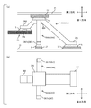
上記各実施の形態では、断面が略T字形状の第一接続体60が用いられていたが、本実施の形態の第一接続体60は、図10に示すように、第一ヘッド部61から他方側に延びた4つの支持部65(65a-65d)を有している。支持体65は、第一導体層又は第一基板に当接するようになっている。その他の構成については、上記各実施の形態で説明したあらゆる態様を採用することができる。上記各実施の形態で説明した部材については同じ符号を用いて説明する。
本実施の形態では4つの支持部65が利用されている態様を用いて説明するが、これに限られることはなく、1、2、3又は5つ以上の支持部65が用いられてもよい。
本実施の形態のように第一ヘッド部61から延びた支持部65が設けられている場合には、第二電子素子23の実装時又は第二電子素子23を実装した後で第二電子素子23の重みによって第一接続体60が傾いてしまうことを防止できる。また、このように支持部65が第一基板11又は第一導体層12に当接することで、放熱性を高めることができる。特に支持部65が第一導体層12に当接する場合には、放熱効果をより高めることができる点で有益である。
また、本実施の形態のように複数の支持部65が設けられている場合には、第一接続体60をより安定に設けることができ、かつより高い放熱効果を実現できる点で有益である。
支持部65の各々は、面方向で延び、第一基板11又は第一導体層12と当接する支持基端部69(69a-69d)を有してもよい。また、複数の支持部65の各々に支持基端部69が設けられる必要はなく、複数の支持部65のうちの一部に支持基端部69が設けられ、残部に支持基端部69が設けられないようにしてもよい。
このような支持基端部69が設けられている場合には、第一接続体60をよりバランスよく第一基板11又は第一導体層12に配置することができ、また支持基端部69で第一基板11又は第一導体層12との接触面積を増やすことができることから、放熱効果を高めることできる。
支持部65の各々は第一導体層12に当接してもよい。支持部65に接続される第一導体層12が他の第一導体層12、第二導体層22、第一電子素子13及び第二電子素子23に電気的に接続されておらず電気的な機能を果たさない態様を採用した場合には、支持部65が導通して予想していない挙動を第一電子素子13及び第二電子素子23が示すことを防止できる点で有益である。
支持部65の各々は、第一ヘッド部61から面方向に延びた面方向支持部166(166a-166d)と、面方向支持部166の端部から高さ方向(第一方向)に延びた高さ方向支持部165(165a-165d)とを有してもよい(後述する第6の実施の形態も参照)。なお、面方向支持部166は、第一ヘッド部61よりも幅方向の長さが短くなっている部分のことを意味している。
支持部65は、面方向支持部166を有さず、第一ヘッド部61から高さ方向(第一方向)に延びた高さ方向支持部165だけを有してもよい。
上記各実施の形態で説明した当接体250を採用する場合に本実施の形態のように支持部65を用いることは有益である。当接体250は第二電子素子23の一方側の面に直接又は導電性接着剤5等を介して間接的に設けられることになるが、第二電子素子23が安定した状態で配置されていないと、第二基板21を当接体250によって一方側に押し付ける際に第二電子素子23が傾いてしまったりすることがある。他方、本実施の形態によれば、第一接続体60が支持部65を有しているので、第二電子素子23を当接体250によって他方側に押圧した場合であっても、第二電子素子23が傾いたりすることを防止できる。その結果、第二基板21を当接体250によって一方側に安定して押し付けることができる。
第一当接体260に関して言えば、当接基端部263が第二電子素子23の一方側の面に当接することになるが、熱が加わることで第一基板11及び第二基板21が反ったり歪んだりしようとした際に、第二電子素子23に当接基端部263を介して力が加わることになる。この点、本実施の形態では第一接続体60が支持部65を有しているので、第二電子素子23が傾いたりすることを防止でき、その結果、第二基板21を第一基板側当接部261によって一方側に安定して押し付けることができる。
第二当接体270に関して言えば、第一当接部材271が第二電子素子23の一方側の面に当接することになるが、熱が加わることで第一基板11及び第二基板21が反ったり歪んだりしようとした際に、第二電子素子23に第一当接部材271を介して力が加わることになる。この点、本実施の形態では第一接続体60が支持部65を有しているので、第二電子素子23が傾いたりすることを防止でき、その結果、第二基板21を第二当接部材272によって一方側に安定して押し付けることができる。
第9の実施の形態
次に、本発明の第9の実施の形態について説明する。
次に、本発明の第9の実施の形態について説明する。
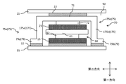
上記各実施の形態では第二柱部72を有する断面が略T字形状からなる第二接続体70を用いて説明したが、本実施の形態では、図11に示すように、第二接続体70は、第二ヘッド部71から他方側に延びる延在部75(75a,75b)を有している。その他の構成については、上述した各実施の形態で説明したあらゆる態様を採用することができる。上述した各実施の形態で説明した部材については同じ符号を用いて説明する。
本実施の形態では2つの延在部75が利用されている態様を用いて説明するが、これに限られることはなく、1つ又は3つ以上の延在部75が用いられてもよい。
本実施の形態によれば、延在部75が設けられていることから、第二電子素子23からの熱を効率よく放熱することができ、第二接続体70によっても高い放熱効果を実現できる。また、本実施の形態のように複数の延在部75が設けられている場合には、より高い放熱効果を実現できる点で有益である。
延在部75の各々は第一導体層12に当接してもよい。延在部75に接続される第一導体層12は、他の第一導体層12及び第一電子素子13に電気的に接続されていなくてもよい。
延在部75の各々は、面方向で延び、第一基板11又は第一導体層12と当接する延在基端部79(79a,79b)を有してもよい。また、複数の延在部75の各々に延在基端部79が設けられる必要はなく、複数の延在部75のうちの一部に延在基端部79が設けられ、残部に延在基端部79が設けられないようにしてもよい。
このような延在基端部79が設けられている場合には、第二接続体70をよりバランスよく第一基板11又は第一導体層12に配置することができ、また延在基端部79で第一基板11又は第一導体層12との接触面積を増やすことができることから、放熱効果を高めることできる。
本実施の形態のように複数の延在部75を有する第二接続体70を採用した場合には、当接体250と同様、第二基板21を一方側に押し返す反発力を付与できるようになる。つまり、前述したように熱が加わることで第一基板11及び第二基板21が反ったり歪んだりしようとする力が加わるが、複数の延在部75を有する第二接続体70を用いることで、第一当接体260及び第二当接体270による作用に加えて、第二接続体70によっても第一基板11及び第二基板21の反りや歪みを防止できる点で有益である。
なお、本実施の形態の延在部75は、第二ヘッド部71から高さ方向(第一方向)に延びた高さ方向延在部175(175a,175b)を有している。
第10の実施の形態
次に、本発明の第10の実施の形態について説明する。
次に、本発明の第10の実施の形態について説明する。
第8の実施の形態では支持部65が設けられ、第9の実施の形態では延在部75が設けられる態様であったが、支持部65及び延在部75がともに採用されてもよい。本実施の形態では、図12乃至図14に示すように、3つの支持部65及び3つの延在部75が用いられている態様を一例として挙げて説明する。その他の構成については、上述した各実施の形態で説明したあらゆる態様を採用することができる。上述した各実施の形態で説明した部材については同じ符号を用いて説明する。
本実施の形態で示すように、延在部75は、第二ヘッド部71から面方向に延びた面方向延在部176と、面方向延在部176から高さ方向(第一方向)に延びた高さ方向延在部175とを有してもよい。なお、面方向延在部176は、第二ヘッド部71よりも幅方向の大きさが小さくなっている部分のことを意味している。
本実施の形態によれば、当接体250を有することによる効果と、前述した複数の支持部65を有することによる効果と複数の延在部75を有することによる効果を得ることができる点で有益である。
上述した各実施の形態の記載及び図面の開示は、請求の範囲に記載された発明を説明するための一例に過ぎず、上述した実施の形態の記載又は図面の開示によって請求の範囲に記載された発明が限定されることはない。また、出願当初の請求項の記載はあくまでも一例であり、明細書、図面等の記載に基づき、請求項の記載を適宜変更することもできる。
11 第一基板
12 第一導体層
13 第一電子素子
21 第二基板
22 第二導体層
23 第二電子素子
60 第一接続体
250 当接体
260 第一当接体
261 第一基板側当接部
262 第二基板側当接部
263 当接基端部
265 第一凸部
266 脚部
267 脚当接部
270 第二当接体
271 第一当接部材
272 第二当接部材
273 連結部材
12 第一導体層
13 第一電子素子
21 第二基板
22 第二導体層
23 第二電子素子
60 第一接続体
250 当接体
260 第一当接体
261 第一基板側当接部
262 第二基板側当接部
263 当接基端部
265 第一凸部
266 脚部
267 脚当接部
270 第二当接体
271 第一当接部材
272 第二当接部材
273 連結部材
Claims (7)
- 第一基板と、
前記第一基板の一方側に設けられた第一電子素子と、
前記第一電子素子の一方側に設けられた第一接続体と、
前記第一接続体の一方側に設けられた第二電子素子と、
前記第二電子素子の一方側に設けられた第二基板と、
前記第二電子素子の一方側の面に当接し、前記第二基板に対して一方側に向かう力を付与できる当接体と、
を備え、
前記当接体は、前記第二電子素子と外部装置に接続可能な端子部とを電気的に接続することを特徴とする電子モジュール。 - 前記第一基板と記第一電子素子との間に設けられた第一導体層と、
前記第二基板の他方側に設けられた第二導体層と、をさらに備え、
前記当接体は第一当接体を有し、
前記第一当接体は、前記第二電子素子の一方側の面に当接する当接基端部と、前記当接基端部から一方側に延び、前記第二導体層又は前記第二基板に当接する第二基板側当接部と、前記第二基板側当接部から他方側に延び、前記第一導体層又は前記第一基板に当接する第一基板側当接部とを有することを特徴とする請求項1に記載の電子モジュール。 - 前記第一基板は金属基板からなり、
前記第二基板は金属基板からなり、
前記当接体は第一当接体を有し、
前記第一当接体は、前記第二電子素子の一方側の面に当接する当接基端部と、前記当接基端部から一方側に延び、前記第二基板に当接する第二基板側当接部と、前記第二基板側当接部から他方側に延び、前記第一基板に当接する第一基板側当接部とを有することを特徴とする請求項1に記載の電子モジュール。 - 前記第二基板側当接部は一方側に突出した第一凸部を有し、
前記第二基板側当接部は導電性接着剤を介して前記第二導体層に当接することを特徴とする請求項2又は3のいずれかに記載の電子モジュール。 - 前記第一当接体は、他方側に延びた一つ以上の脚部を有し、
前記脚部は、前記第一導体層又は前記第一基板に当接することを特徴とする請求項2乃至4のいずれか1項に記載の電子モジュール。 - 前記脚部が前記第一導体層又は前記第一基板に当接する面積は、前記第一基板側当接部が前記第一導体層又は前記第一基板に当接する面積よりも小さいことを特徴とする請求項5に記載の電子モジュール。
- 前記当接体は第二当接体を有し、
前記第二当接体は、前記第二電子素子の一方側の面に当接する第一当接部材と、前記第一当接部材の一方側に設けられた第二当接部材と、前記第一当接部材と前記第二当接部材とを連結し、前記第二当接部材に一方側に向かう力を付与できる連結部材とを有することを特徴とする請求項1乃至6のいずれか1項に記載の電子モジュール。
Priority Applications (6)
| Application Number | Priority Date | Filing Date | Title |
|---|---|---|---|
| PCT/JP2017/018835 WO2018211686A1 (ja) | 2017-05-19 | 2017-05-19 | 電子モジュール |
| US16/060,279 US11309273B2 (en) | 2017-05-19 | 2017-05-19 | Electronic module |
| CN201780005103.9A CN109287129B (zh) | 2017-05-19 | 2017-05-19 | 电子模块 |
| JP2018509873A JP6473271B1 (ja) | 2017-05-19 | 2017-05-19 | 電子モジュール |
| TW107115219A TWI681533B (zh) | 2017-05-19 | 2018-05-04 | 電子模組 |
| NL2020929A NL2020929B1 (en) | 2017-05-19 | 2018-05-15 | Electronic module |
Applications Claiming Priority (1)
| Application Number | Priority Date | Filing Date | Title |
|---|---|---|---|
| PCT/JP2017/018835 WO2018211686A1 (ja) | 2017-05-19 | 2017-05-19 | 電子モジュール |
Publications (1)
| Publication Number | Publication Date |
|---|---|
| WO2018211686A1 true WO2018211686A1 (ja) | 2018-11-22 |
Family
ID=63207817
Family Applications (1)
| Application Number | Title | Priority Date | Filing Date |
|---|---|---|---|
| PCT/JP2017/018835 Ceased WO2018211686A1 (ja) | 2017-05-19 | 2017-05-19 | 電子モジュール |
Country Status (6)
| Country | Link |
|---|---|
| US (1) | US11309273B2 (ja) |
| JP (1) | JP6473271B1 (ja) |
| CN (1) | CN109287129B (ja) |
| NL (1) | NL2020929B1 (ja) |
| TW (1) | TWI681533B (ja) |
| WO (1) | WO2018211686A1 (ja) |
Cited By (1)
| Publication number | Priority date | Publication date | Assignee | Title |
|---|---|---|---|---|
| US12057376B2 (en) | 2020-11-02 | 2024-08-06 | Infineon Technologies Ag | Three level interconnect clip |
Families Citing this family (1)
| Publication number | Priority date | Publication date | Assignee | Title |
|---|---|---|---|---|
| DE102019115857A1 (de) * | 2019-06-11 | 2020-12-17 | Infineon Technologies Ag | Halbleitergehäuse und verfahren zur herstellung eines halbleitergehäuses |
Citations (5)
| Publication number | Priority date | Publication date | Assignee | Title |
|---|---|---|---|---|
| JP2005302951A (ja) * | 2004-04-09 | 2005-10-27 | Toshiba Corp | 電力用半導体装置パッケージ |
| US20120063107A1 (en) * | 2010-09-15 | 2012-03-15 | Shutesh Krishnan | Semiconductor component and method of manufacture |
| WO2012096066A1 (ja) * | 2011-01-11 | 2012-07-19 | カルソニックカンセイ株式会社 | パワー半導体モジュール |
| JP2015220429A (ja) * | 2014-05-21 | 2015-12-07 | ローム株式会社 | 半導体装置 |
| JP2016066700A (ja) * | 2014-09-25 | 2016-04-28 | 株式会社日立製作所 | パワー半導体モジュール |
Family Cites Families (15)
| Publication number | Priority date | Publication date | Assignee | Title |
|---|---|---|---|---|
| JP3510841B2 (ja) * | 2000-05-09 | 2004-03-29 | 三洋電機株式会社 | 板状体、リードフレームおよび半導体装置の製造方法 |
| JP4134893B2 (ja) * | 2003-12-05 | 2008-08-20 | 松下電器産業株式会社 | 電子素子パッケージ |
| JP4916745B2 (ja) | 2006-03-28 | 2012-04-18 | ルネサスエレクトロニクス株式会社 | 半導体装置の製造方法 |
| JP5169071B2 (ja) * | 2007-08-21 | 2013-03-27 | セイコーエプソン株式会社 | 電子部品、電子装置、電子部品の実装構造体及び電子部品の実装構造体の製造方法 |
| US20090127676A1 (en) | 2007-11-16 | 2009-05-21 | Gomez Jocel P | Back to Back Die Assembly For Semiconductor Devices |
| JP5197219B2 (ja) * | 2007-11-22 | 2013-05-15 | パナソニック株式会社 | 半導体装置およびその製造方法 |
| US8492884B2 (en) * | 2010-06-07 | 2013-07-23 | Linear Technology Corporation | Stacked interposer leadframes |
| JP5414644B2 (ja) | 2010-09-29 | 2014-02-12 | 三菱電機株式会社 | 半導体装置 |
| US20120200281A1 (en) | 2011-02-07 | 2012-08-09 | Texas Instruments Incorporated | Three-Dimensional Power Supply Module Having Reduced Switch Node Ringing |
| WO2013153745A1 (ja) * | 2012-04-10 | 2013-10-17 | パナソニック株式会社 | 電極接合方法、電極接合構造体の製造方法、および電極接合構造体の製造システム |
| JP2014045157A (ja) | 2012-08-29 | 2014-03-13 | Hitachi Automotive Systems Ltd | パワー半導体モジュール |
| US8932911B2 (en) * | 2013-02-27 | 2015-01-13 | GlobalFoundries, Inc. | Integrated circuits and methods for fabricating integrated circuits with capping layers between metal contacts and interconnects |
| WO2014132397A1 (ja) * | 2013-02-28 | 2014-09-04 | 新電元工業株式会社 | モジュール、モジュール組合体及びモジュールの製造方法 |
| US9966330B2 (en) * | 2013-03-14 | 2018-05-08 | Vishay-Siliconix | Stack die package |
| DE102014104496B4 (de) * | 2014-03-31 | 2019-07-18 | Semikron Elektronik Gmbh & Co. Kg | Vorrichtung zur schweißtechnischen Verbindung von Anschlusselementen mit dem Substrat eines Leistungshalbleitermoduls und zugehöriges Verfahren |
-
2017
- 2017-05-19 JP JP2018509873A patent/JP6473271B1/ja active Active
- 2017-05-19 WO PCT/JP2017/018835 patent/WO2018211686A1/ja not_active Ceased
- 2017-05-19 US US16/060,279 patent/US11309273B2/en active Active
- 2017-05-19 CN CN201780005103.9A patent/CN109287129B/zh active Active
-
2018
- 2018-05-04 TW TW107115219A patent/TWI681533B/zh active
- 2018-05-15 NL NL2020929A patent/NL2020929B1/en active
Patent Citations (5)
| Publication number | Priority date | Publication date | Assignee | Title |
|---|---|---|---|---|
| JP2005302951A (ja) * | 2004-04-09 | 2005-10-27 | Toshiba Corp | 電力用半導体装置パッケージ |
| US20120063107A1 (en) * | 2010-09-15 | 2012-03-15 | Shutesh Krishnan | Semiconductor component and method of manufacture |
| WO2012096066A1 (ja) * | 2011-01-11 | 2012-07-19 | カルソニックカンセイ株式会社 | パワー半導体モジュール |
| JP2015220429A (ja) * | 2014-05-21 | 2015-12-07 | ローム株式会社 | 半導体装置 |
| JP2016066700A (ja) * | 2014-09-25 | 2016-04-28 | 株式会社日立製作所 | パワー半導体モジュール |
Cited By (1)
| Publication number | Priority date | Publication date | Assignee | Title |
|---|---|---|---|---|
| US12057376B2 (en) | 2020-11-02 | 2024-08-06 | Infineon Technologies Ag | Three level interconnect clip |
Also Published As
| Publication number | Publication date |
|---|---|
| US20210175198A1 (en) | 2021-06-10 |
| JP6473271B1 (ja) | 2019-02-20 |
| TW201911529A (zh) | 2019-03-16 |
| NL2020929B1 (en) | 2019-03-27 |
| US11309273B2 (en) | 2022-04-19 |
| JPWO2018211686A1 (ja) | 2019-06-27 |
| CN109287129A (zh) | 2019-01-29 |
| NL2020929A (en) | 2018-11-23 |
| CN109287129B (zh) | 2022-04-08 |
| TWI681533B (zh) | 2020-01-01 |
Similar Documents
| Publication | Publication Date | Title |
|---|---|---|
| JP6732118B2 (ja) | 電子モジュール及び電子モジュールの製造方法 | |
| JP2004047561A (ja) | 光導電スイッチモジュールおよびその製造方法 | |
| JP6473271B1 (ja) | 電子モジュール | |
| JP6402281B1 (ja) | 電子モジュール、接続体の製造方法及び電子モジュールの製造方法 | |
| JP6511584B2 (ja) | チップモジュールの製造方法 | |
| TWI683373B (zh) | 電子模組 | |
| JP6463558B1 (ja) | 電子モジュール、リードフレーム及び電子モジュールの製造方法 | |
| JP6523567B1 (ja) | 電子モジュール | |
| JP6952042B2 (ja) | 電子モジュール | |
| JP7018459B2 (ja) | 電子モジュール | |
| JP6999707B2 (ja) | 電子モジュール | |
| CN112368829B (zh) | 电子模块 | |
| JP7018965B2 (ja) | 電子モジュール | |
| JPWO2019142254A1 (ja) | 電子モジュール | |
| JPWO2019142257A1 (ja) | 電子モジュール |
Legal Events
| Date | Code | Title | Description |
|---|---|---|---|
| ENP | Entry into the national phase |
Ref document number: 2018509873 Country of ref document: JP Kind code of ref document: A |
|
| 121 | Ep: the epo has been informed by wipo that ep was designated in this application |
Ref document number: 17910136 Country of ref document: EP Kind code of ref document: A1 |
|
| NENP | Non-entry into the national phase |
Ref country code: DE |
|
| 122 | Ep: pct application non-entry in european phase |
Ref document number: 17910136 Country of ref document: EP Kind code of ref document: A1 |