WO2018207620A1 - 蓄電素子の接続構造および蓄電モジュール - Google Patents
蓄電素子の接続構造および蓄電モジュール Download PDFInfo
- Publication number
- WO2018207620A1 WO2018207620A1 PCT/JP2018/016710 JP2018016710W WO2018207620A1 WO 2018207620 A1 WO2018207620 A1 WO 2018207620A1 JP 2018016710 W JP2018016710 W JP 2018016710W WO 2018207620 A1 WO2018207620 A1 WO 2018207620A1
- Authority
- WO
- WIPO (PCT)
- Prior art keywords
- circuit board
- electrode
- power
- pattern
- storage element
- Prior art date
- Legal status (The legal status is an assumption and is not a legal conclusion. Google has not performed a legal analysis and makes no representation as to the accuracy of the status listed.)
- Ceased
Links
Images


Classifications
-
- H—ELECTRICITY
- H01—ELECTRIC ELEMENTS
- H01G—CAPACITORS; CAPACITORS, RECTIFIERS, DETECTORS, SWITCHING DEVICES, LIGHT-SENSITIVE OR TEMPERATURE-SENSITIVE DEVICES OF THE ELECTROLYTIC TYPE
- H01G9/00—Electrolytic capacitors, rectifiers, detectors, switching devices, light-sensitive or temperature-sensitive devices; Processes of their manufacture
- H01G9/004—Details
- H01G9/008—Terminals
-
- H—ELECTRICITY
- H01—ELECTRIC ELEMENTS
- H01G—CAPACITORS; CAPACITORS, RECTIFIERS, DETECTORS, SWITCHING DEVICES, LIGHT-SENSITIVE OR TEMPERATURE-SENSITIVE DEVICES OF THE ELECTROLYTIC TYPE
- H01G2/00—Details of capacitors not covered by a single one of groups H01G4/00-H01G11/00
- H01G2/02—Mountings
- H01G2/04—Mountings specially adapted for mounting on a chassis
-
- H—ELECTRICITY
- H01—ELECTRIC ELEMENTS
- H01G—CAPACITORS; CAPACITORS, RECTIFIERS, DETECTORS, SWITCHING DEVICES, LIGHT-SENSITIVE OR TEMPERATURE-SENSITIVE DEVICES OF THE ELECTROLYTIC TYPE
- H01G11/00—Hybrid capacitors, i.e. capacitors having different positive and negative electrodes; Electric double-layer [EDL] capacitors; Processes for the manufacture thereof or of parts thereof
- H01G11/08—Structural combinations, e.g. assembly or connection, of hybrid or EDL capacitors with other electric components, at least one hybrid or EDL capacitor being the main component
-
- H—ELECTRICITY
- H01—ELECTRIC ELEMENTS
- H01G—CAPACITORS; CAPACITORS, RECTIFIERS, DETECTORS, SWITCHING DEVICES, LIGHT-SENSITIVE OR TEMPERATURE-SENSITIVE DEVICES OF THE ELECTROLYTIC TYPE
- H01G11/00—Hybrid capacitors, i.e. capacitors having different positive and negative electrodes; Electric double-layer [EDL] capacitors; Processes for the manufacture thereof or of parts thereof
- H01G11/10—Multiple hybrid or EDL capacitors, e.g. arrays or modules
-
- H—ELECTRICITY
- H01—ELECTRIC ELEMENTS
- H01G—CAPACITORS; CAPACITORS, RECTIFIERS, DETECTORS, SWITCHING DEVICES, LIGHT-SENSITIVE OR TEMPERATURE-SENSITIVE DEVICES OF THE ELECTROLYTIC TYPE
- H01G11/00—Hybrid capacitors, i.e. capacitors having different positive and negative electrodes; Electric double-layer [EDL] capacitors; Processes for the manufacture thereof or of parts thereof
- H01G11/74—Terminals, e.g. extensions of current collectors
- H01G11/76—Terminals, e.g. extensions of current collectors specially adapted for integration in multiple or stacked hybrid or EDL capacitors
-
- H—ELECTRICITY
- H01—ELECTRIC ELEMENTS
- H01G—CAPACITORS; CAPACITORS, RECTIFIERS, DETECTORS, SWITCHING DEVICES, LIGHT-SENSITIVE OR TEMPERATURE-SENSITIVE DEVICES OF THE ELECTROLYTIC TYPE
- H01G11/00—Hybrid capacitors, i.e. capacitors having different positive and negative electrodes; Electric double-layer [EDL] capacitors; Processes for the manufacture thereof or of parts thereof
- H01G11/78—Cases; Housings; Encapsulations; Mountings
- H01G11/82—Fixing or assembling a capacitive element in a housing, e.g. mounting electrodes, current collectors or terminals in containers or encapsulations
-
- H—ELECTRICITY
- H01—ELECTRIC ELEMENTS
- H01G—CAPACITORS; CAPACITORS, RECTIFIERS, DETECTORS, SWITCHING DEVICES, LIGHT-SENSITIVE OR TEMPERATURE-SENSITIVE DEVICES OF THE ELECTROLYTIC TYPE
- H01G9/00—Electrolytic capacitors, rectifiers, detectors, switching devices, light-sensitive or temperature-sensitive devices; Processes of their manufacture
- H01G9/004—Details
- H01G9/08—Housing; Encapsulation
Definitions
- the technology disclosed in this specification relates to a connection structure of a storage element and a storage module.
- Patent Document 1 Conventionally, for example, a capacitor device disclosed in Patent Document 1 is known as an auxiliary power source used for emergency when the main power source becomes unusable.
- capacitors capacitors having electrodes and safety valves for releasing abnormal pressure are accommodated in a storage case. And on the top surface, individual bus bars are arranged between the electrodes and fixed with screws, and a circuit board for controlling the balance of each storage element is fixed in the area avoiding each electrode and safety valve And is held integrally with the capacitor.
- the technology disclosed in the present specification has been completed based on the above-described circumstances, and the storage unit connection structure and the storage module that can hold the circuit board while connecting the storage elements are reduced in the number of parts. It aims at providing at low cost.
- a connection structure for connecting electrodes of a plurality of power storage elements includes a through hole through which the electrode is inserted and a power pattern, and is mounted on the plurality of power storage elements.
- the circuit board is fastened to the power storage element and the power pattern is electrically connected to the electrode simply by placing the circuit board on the electrodes of the plurality of power storage elements and screwing the fastening member to the electrode. Since it can be connected, the number of parts and man-hours can be reduced. And since the spacer is provided in the through-hole of the circuit board, the pressing force with respect to the circuit board of a fastening member can be restrict
- the power pattern includes a plurality of contact parts exposed on the surface of the circuit board, and the fastening member presses the plurality of contact parts against the electrodes of the plurality of power storage elements through the circuit board. Good.
- a conductive plating layer is formed on the inner wall of the through hole, and the power pattern is arranged on the electrode side and pressed against the electrode by the first power pattern and the first power via the insulating layer. And a second power pattern that is stacked on the power pattern and electrically connected to the first power pattern via the plating layer.
- the second power pattern formed in a layer different from the first power pattern can also be connected to the electrode. Thereby, a bigger electric current can be sent.
- the circuit board may be provided with a control circuit for controlling the state of the power storage element, and a signal pattern for connecting the power pattern and the control circuit may be formed.
- This configuration eliminates the need for an electric wire for connecting the control circuit and the electrodes, thereby reducing the number of components.
- the power storage module includes a plurality of power storage elements, a case that houses the plurality of power storage elements, a through-hole through which an electrode of each power storage element is inserted, and a power pattern.
- a circuit board a shaft portion inserted through the through-hole and screwed into the electrode of the power storage element, and the power pattern being pressed against the electrode of the power storage element through the circuit board integrated with the shaft portion And a cap disposed between the power storage element and the circuit board.
- the power storage module includes: a fastening member including a pressing portion configured to support; a spacer disposed in the through hole to support the pressing portion; and a cap disposed between the power storage element and the circuit board.
- the power storage element is provided with a safety valve that opens the internal space when the internal space exceeds a predetermined pressure, and the cap is disposed between the circuit board and the safety valve to provide the safety valve.
- a board support part for supporting the circuit board together with the electrodes may be provided on the cap so as to protrude toward the circuit board.
- AA sectional view of FIG. BB sectional view of FIG. Exploded front view of the connection structure between electrodes
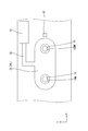
- Top view showing power and signal patterns
- Front view showing the connection structure between electrodes
- the top view which shows the electrical storage module of Embodiment 2.
- the power storage module 1 of this embodiment is mounted on a vehicle as a sub power source when the main power source becomes inoperable.
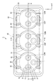
- the power storage module 1 includes a plurality of (three in the present embodiment) capacitors 10 (an example of a power storage element) accommodated in a case 60.
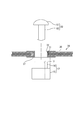
- the circuit board 30 is placed and fastened to the electrode 12 with a bolt 50.
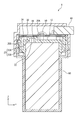
- a cap 20 is disposed between the circuit board 30 and the capacitor 10.
- the circuit board 30 is arranged to electrically connect the capacitors 10 and to control the state of the capacitors 10.
- the circuit board 30 is not shown in detail, and only the outline is indicated by a two-dot chain line C.
- the case 60 has a rectangular parallelepiped shape with an upper surface opening, and a plurality of (three in the present embodiment) cylindrical capacitor housing portions 61 are provided side by side inside the case 60.
- the upper surface of each capacitor housing 61 is opened, and a pair of guide ribs 62 for positioning the cap 20 are provided along the front-rear direction, as shown in FIG. .
- Each of the capacitors 10A to 10C has a cylindrical capacitor body portion disposed in the capacitor housing portion 61, and is accommodated with the electrode 12 facing upward and the positive electrode P and the negative electrode N alternately disposed side by side. Yes.
- a safety valve 11 is provided behind the electrode 12, and is opened when the capacitor 10 becomes a predetermined internal pressure or higher due to heat generation or the like, and gas or the like is ejected from the capacitor 10.
- Each capacitor 10 is connected in series by a power pattern on a circuit board 30 to be described later, and is connected to the outside from the electrodes 12AP and 12CN at both ends via a connector 40 mounted on the board.
- each electrode 12 is integrally provided with a base portion 15 protruding from the capacitor 10 and a spacer portion 16 protruding from the base portion 15 and having a smaller diameter than the base portion 15.
- the electrode 12 has an insertion hole 13 through which the bolt 50 is inserted.
- the cap 20 includes a disc-shaped cap body 20 ⁇ / b> A and a peripheral wall portion 20 ⁇ / b> B that extends downward from the peripheral edge and surrounds the peripheral surface of the capacitor 10.
- the cap body 20 ⁇ / b> A is placed on the upper surface of the capacitor 10 with each electrode 12 inserted through the two holes 21.
- a safety cover portion 22 is provided behind the hole portion 21 and is disposed between the safety valve 11 and the circuit board 30.
- the safety cover portion 22 is formed in a shape in which the lower surface of the cap main body 20A is formed in a circular shape, and is formed one step higher than the upper surface of the cap main body 20A on the upper surface side. As a result, the safety cover portion 22 has a thickness comparable to that of the cap body 20A.
- an escape groove 23 for guiding the gas ejected from the safety valve 11 in a direction away from the circuit board 30 is provided inside the cap 20 (on the side facing the capacitor 10).
- the escape groove portion 23 includes a horizontal escape portion 23A extending rearward from the safety cover portion 22, and a vertical escape portion 23B extending downward from the rear end of the horizontal escape portion.
- the horizontal relief portion 23A is provided continuously from the safety cover portion 22, and has a shape in which the lower surface of the cap body 20A is formed in a groove shape.
- the vertical escape portion 23B is provided continuously from the rear end of the horizontal escape portion 23A, and has a shape in which the inner wall of the peripheral wall portion 20B of the cap 20 is formed in a groove shape.
- the space defined between the safety cover portion 22 and the capacitor 10 is the space defined between the horizontal escape portion 23A and the capacitor 10 and between the vertical escape portion 23B and the capacitor main body portion. It communicates with the lower space of the cap 20 through a defined space.
- the gas ejected from the safety valve 11 passes through these spaces (that is, guided in a direction away from the circuit board 30 by the safety cover portion 22 and the escape groove portion 23), and is released to the space below the cap 20. .
- a locking portion 24 extends from the front end and the rear end of the peripheral wall portion, and a locking piece provided near the front end of the peripheral wall portion is locked from the inside to a locking receiving portion provided near the upper end of the case 60.
- a pair of support ribs 25 are respectively provided along the front-rear direction and are erected upward on the front side and the rear side of the cap body 20A. And a circuit board 30 to be described later are supported.
- the circuit board 30 has a rectangular flat plate shape slightly smaller than the upper opening of the case 60 and is fitted into the case 60 and supported by the base portion 15 of the electrode 12 and the support rib 25 of the cap 20.
- a plurality (six in this embodiment) of through holes 31 are provided in the circuit board 30 side by side.
- the through-hole 31 is formed in a circular shape having a diameter slightly larger than that of the spacer portion 16 of the electrode 12 and smaller than that of the base portion 15. Spacer portions 16 are inserted into the respective through holes 31 of the circuit board 30.
- the upper surface opening of the insertion hole 13 is exposed in the spacer portion 16 disposed in the through hole 31, and a bolt 50 is inserted therein to fasten the circuit board 30 to the electrode 12.
- the bolt 50 is a well-known one that includes a head 51 (an example of a pressing portion) and a shaft portion 52 that is formed integrally with the head 51.
- the shaft portion 52 is inserted into and screwed into the electrode 12, and the head portion 51 is in contact with the upper surface of the circuit board 30 and presses it against the base portion 15 of the electrode 12. Further, the lower surface of the head 51 is also in contact with and supported by the upper surface of the spacer portion 16 of the electrode 12.
- a conductive plating layer 32 is provided on the inner peripheral surface (inner wall) of each through hole 31.
- the thickness of the plated layer 32 is not considered, and the inner peripheral surface of the plated layer 32 is described as the inner peripheral surface of the through hole 31.
- the circuit board 30 is provided with a power pattern for conducting power from the capacitor 10 and a signal pattern 36 for conducting a signal related to the state of the capacitor 10. ing.
- the power pattern includes an interelectrode pattern 34 for connecting adjacent electrodes 12.
- the inter-electrode pattern 34 is formed from the peripheral region of one through hole 31 to the peripheral region of the through hole 31 adjacent thereto.
- the oval interelectrode pattern 34L surrounds the negative electrode 12AN of the first capacitor 10A and the positive electrode 10BP of the second capacitor 10B, and the oval interelectrode pattern 34R is also the second capacitor 10B.
- the negative electrode 10BN of the third capacitor 10C and the positive electrode 10CP of the third capacitor 10C are surrounded. Since the interelectrode pattern 34L and the interelectrode pattern 34R have the same configuration, description and illustration of the interelectrode pattern 34R are omitted.
- the circuit board 30 of the present embodiment is a laminated board in which a plurality of power patterns are laminated via an insulating layer.
- the inter-electrode pattern 34L is formed by vertically stacking inter-electrode patterns 34A to 34D having the same shape, of which the lowermost first inter-electrode pattern 34A (an example of a first power pattern) ) Includes a contact portion 37 that is exposed on the back surface of the circuit board 30 and is electrically connected to the electrode 12 by being pressed against the electrode 12 by the bolt 50 through the circuit board 30.
- the interelectrode patterns 34A to 34D and the plated layer 32 of each through hole 31 are electrically connected to form one connection conductor as a whole.
- both electrodes 12 are directly connected by the first inter-electrode pattern 34A, and are connected via the plating layer 32 depending on the second inter-electrode patterns 34B to 34D (an example of the second power pattern) higher than that. Has been.
- the entire first interelectrode pattern 34A is exposed on the lower surface side of the circuit board 30.
- the contact portion 37 pressing contact with the electrode 12
- the region formed between the contact points 37 may be embedded in the circuit board 30.
- the first inter-electrode pattern 34A may be only the contact portion 37, and the portion between the two contact portions 37 may be omitted. Thereby, the area occupied by the first inter-electrode pattern 34A on the lower surface side of the circuit board 30 can be reduced, and the degree of freedom in designing the mounting position of other electronic components can be increased.
- the inter-electrode pattern 34 preferably has a cross-sectional area corresponding to the amount of current obtained from the capacitor 10. However, for example, when the inter-electrode pattern 34 is used only for a short time as a sub power source as in the present embodiment, the inter-electrode pattern 34 is obtained from the capacitor 10. It is not necessary to have a cross-sectional area corresponding to the amount of current to be obtained.
- the number of stacked second electrode patterns 34B to 34D is not limited to the three layers as described above, but can be determined as appropriate according to the required allowable current, and the second electrode patterns 34 are not provided. May be. When the second inter-electrode pattern 34 is not provided, the plated layer 32 of the through hole 31 can be omitted.
- the external connection pattern individually surrounds the electrodes 12 at both ends of the capacitor 10 (the positive electrode 12AP of the first capacitor 10A and the negative electrode 10CN of the third capacitor 10C) and extends to the vicinity of the external power output terminal (not shown) of the connector 40. It is formed out. Since the external connection pattern has the same configuration as the inter-electrode pattern 34 except that only one electrode 12 is surrounded, description and illustration are omitted.
- the signal pattern 36 is for electrically connecting a control device for controlling the operation of the capacitor 10 (for example, ECU (Electronic Control Unit)) and the electrode 12.
- a balance circuit 41 (an example of a control circuit) is formed on the circuit board 30 as a part of the control device, and balances the state of each capacitor 10 based on the state of each capacitor 10.
- the signal pattern 36 is formed by connecting the balance circuit 41 and the inter-electrode pattern 34L.
- the connector 40 includes a signal terminal in addition to the external power output terminal described above. Further, the thermistor 42 for detecting the temperature of the capacitor 10 is further mounted on the circuit board 30. The connector 40 is arranged near the center of the front end of the circuit board 30 (position indicated by a two-dot chain line C in FIG. 1). The thermistor 42 is disposed between the positive electrode 10BP and the negative electrode 10BN of the second capacitor 10B, and regards the detected temperature of the second capacitor 10B as the temperature of the capacitor 10.
- the signal pattern 36 is also formed between these mounted components and the balance circuit 41, but the illustration is omitted.
- the capacitor 10 is accommodated in the capacitor accommodating portion 61 of the case 60, and the positive electrode P and the negative electrode N are alternately arranged side by side.
- the base portion 15 of each electrode 12 is inserted into the hole portion 21 of the cap 20, and the locking portion 24 is fitted between the guide ribs 62 of the case 60, and the locking claw is used as the locking receiving portion of the case 60. Lock.
- the cap 20 is put on the capacitor 10, and the safety cover 22 covers the safety valve 11 and is fixed to the case 60.
- the spacer portion 16 of the electrode 12 is inserted into each through hole 31 of the circuit board 30, and the circuit board 30 is placed on the base portion 15 of the electrode 12.
- the bolt 50 is inserted into the insertion hole 13 of the electrode 12 and screwed into the electrode 12.
- the circuit board 30 is sandwiched between the head portion 51 of the bolt 50 and the base portion 15 of the electrode 12, and the head portion 51 of the bolt 50 abuts on each upper surface of the spacer portion 16 and is supported by the spacer portion 16. It will be in the state. Thereby, the contact portion 37 of the first inter-electrode pattern 34A is pressed against the base portion 15 of the electrode 12, and the electrodes surrounded by the inter-electrode pattern 34 are connected.
- the circuit board that is provided on the capacitor 10 with the through hole 31 and the inter-electrode pattern 34A, and the shaft portion 52 and the shaft portion 52 that are inserted through the through hole 31 and screwed into the electrode 12 of the capacitor 10 are integrated.
- the capacitor 10 is surely provided by the connection structure including the bolt 50 including the head 51 that presses the interelectrode pattern 34A against the electrode 12 and the spacer portion 16 that is disposed in the through hole 31 and supports the head 51.
- the connected power storage module 1 is completed.
- the capacitor 10 and the circuit board 30 are fitted into the case 60 and the bolt 50 is screwed together to fix the circuit board 30 to the capacitor 10 and between the electrodes 12. Can be securely connected. Therefore, for example, the number of parts and man-hours can be reduced compared with the case where the bus bar 170 and the circuit board 30 are separately fixed to the capacitor 10, and cost performance is good.
- a balance circuit 41 for controlling the state of the capacitor 10 is directly formed on the circuit board 30, and a signal pattern 36 for connecting the balance circuit 41 and each power pattern is also directly formed on the circuit board 30. Therefore, for example, it is not necessary to separately provide a detection wire for connection as compared with the case where the balance circuit 41 is provided outside.
- the support rib 25 is provided on the cap 20, rattling of the circuit board 30 can be suppressed and the connection with the electrode 12 can be reliably held. Furthermore, since the cap 20 covers the safety valve 11 of the capacitor 10, it is possible to prevent the gas or the like ejected from the cap 20 from being directly blown onto the circuit board 30, so that the control by the circuit board 30 is possible even in an abnormal state of the capacitor 10. Can be secured.
- the inter-electrode pattern 134 includes only two layers 134 ⁇ / b> A formed on the lower surface of the circuit board 130 and 134 ⁇ / b> D formed on the upper surface, while the bus bar 170 provided with the through hole 131 includes the circuit board 130. And the circuit board 130 and are connected to the electrode 112 by a bolt 150.
- the configuration in which the bus bar 170 is additionally provided as described above is suitable when an allowable current exceeding the power pattern 133 (134) formed in advance on the circuit board 30 is required.
- the bolts for fastening the bus bar 170 and the bolts for fastening the circuit board 130 can be shared, and the number of parts can be reduced.
- a plurality of capacitors 10 are arranged side by side and connected in series by a power pattern.
- the number and arrangement of power storage elements are not limited to this, and for example, six power storages Three elements may be arranged in two rows, connected in series for each row, and the rows may be connected in parallel.
- the power pattern arranged at both ends of the storage element group is formed by integrally forming an interelectrode pattern for connecting electrodes of terminals in each column and an external connection pattern for connecting these to an external device. It is good also as what was done.
- the number of power storage elements (electrodes) connected by one power pattern is not limited to two, and for example, three power storage elements (three electrodes) may be connected by one power pattern.
- one through hole 31 is provided corresponding to each electrode 12 of the capacitor 10, but the through hole is not limited to this. It is good also as a structure which provides a hole and penetrates each electrode in the vicinity of the both ends.
- the bolt 50 is used as the fastening member as the fastening member, but the fastening member is not limited to this.
- the shaft member inserted into the insertion hole and screwed into the electrode, and the vicinity of the upper end of the shaft member The nut may be integrated with the shaft member by being screwed to the nut and abut against the circuit board.
- the spacer portion 16 is integrated with the base portion 15 of the electrode 12, but a spacer (for example, a collar or the like) separate from the electrode (base portion) may be adopted.
- a spacer for example, a collar or the like
- the material of the spacer portion can be selected by giving priority to the robustness over the conductivity, the head of the fastening member can be supported more reliably.
- the plated layer 32 is provided in the through hole 31 of the circuit board 30 to electrically connect the power patterns formed in a plurality of layers.
- the plating layer 32 may be omitted when the pattern for use is securely connected and the spacer has sufficient conductivity. In this case, the spacer becomes a part of the connection conductor for connecting the electrodes.
- SYMBOLS 1,100 Electrical storage module 60: Case part 10, 110: Capacitor (electric storage element) 11: Safety valve 12, 112: Electrode 16, 116: Spacer (spacer) 20, 120: Cap 22: Safety cover portion 23: Relief groove portion 25: Support rib (substrate support portion) 30, 130: Circuit board 31, 131: Through hole 32, 132: Plating layer 34, 134: Interelectrode pattern (power pattern) 37: Contact 40: Connector 41: Balance circuit (control circuit) 42, 142: Thermistor 50, 150: Bolt (fastening member) 51, 151: head (pressing part) 52, 152: Shaft
Landscapes
- Engineering & Computer Science (AREA)
- Power Engineering (AREA)
- Microelectronics & Electronic Packaging (AREA)
- Electric Double-Layer Capacitors Or The Like (AREA)
- Battery Mounting, Suspending (AREA)
Priority Applications (2)
| Application Number | Priority Date | Filing Date | Title |
|---|---|---|---|
| CN201880026842.0A CN110546725B (zh) | 2017-05-11 | 2018-04-25 | 蓄电元件的连接结构及蓄电模块 |
| US16/610,308 US11120947B2 (en) | 2017-05-11 | 2018-04-25 | Connection structure of power storage elements and power storage module |
Applications Claiming Priority (2)
| Application Number | Priority Date | Filing Date | Title |
|---|---|---|---|
| JP2017-094550 | 2017-05-11 | ||
| JP2017094550A JP2018190913A (ja) | 2017-05-11 | 2017-05-11 | 蓄電素子の接続構造および蓄電モジュール |
Publications (1)
| Publication Number | Publication Date |
|---|---|
| WO2018207620A1 true WO2018207620A1 (ja) | 2018-11-15 |
Family
ID=64105302
Family Applications (1)
| Application Number | Title | Priority Date | Filing Date |
|---|---|---|---|
| PCT/JP2018/016710 Ceased WO2018207620A1 (ja) | 2017-05-11 | 2018-04-25 | 蓄電素子の接続構造および蓄電モジュール |
Country Status (4)
| Country | Link |
|---|---|
| US (1) | US11120947B2 (enExample) |
| JP (1) | JP2018190913A (enExample) |
| CN (1) | CN110546725B (enExample) |
| WO (1) | WO2018207620A1 (enExample) |
Families Citing this family (1)
| Publication number | Priority date | Publication date | Assignee | Title |
|---|---|---|---|---|
| DE102024201482A1 (de) | 2024-02-19 | 2025-08-21 | Robert Bosch Gesellschaft mit beschränkter Haftung | Kondensatoreinheit |
Citations (6)
| Publication number | Priority date | Publication date | Assignee | Title |
|---|---|---|---|---|
| JP2002134870A (ja) * | 2000-10-24 | 2002-05-10 | Yonezawa Densen Kk | 大電流用回路基板、その製造方法及び複合回路基板 |
| JP2006252792A (ja) * | 2005-03-08 | 2006-09-21 | Elna Co Ltd | 蓄電素子の接続構造および蓄電素子モジュール |
| JP2007294656A (ja) * | 2006-04-25 | 2007-11-08 | Kyoei Denshi Kk | 高電流用金属回路基板及びその製造方法 |
| JP2010225929A (ja) * | 2009-03-24 | 2010-10-07 | Olympus Corp | 基板固定方法および基板固定具 |
| JP2014520365A (ja) * | 2011-06-17 | 2014-08-21 | コミサリア ア レネルジ アトミク エ オウ エネルジ アルタナティヴ | 電池の中の電池セルを相互接続し測定するためのプリント回路 |
| JP2014197512A (ja) * | 2013-03-29 | 2014-10-16 | 株式会社Gsユアサ | 蓄電装置 |
Family Cites Families (15)
| Publication number | Priority date | Publication date | Assignee | Title |
|---|---|---|---|---|
| JP2536657B2 (ja) * | 1990-03-28 | 1996-09-18 | 三菱電機株式会社 | 電気装置及びその製造方法 |
| KR100357843B1 (ko) * | 1996-07-09 | 2002-12-26 | 마쯔시다덴기산교 가부시키가이샤 | 2차전지및2차전지용실링판조립체 |
| JP4260407B2 (ja) * | 2001-03-30 | 2009-04-30 | 東芝ライテック株式会社 | 電気機器 |
| EP1589547A4 (en) * | 2003-09-18 | 2009-11-25 | Panasonic Corp | CAPACITOR UNIT |
| KR100872616B1 (ko) * | 2004-03-31 | 2008-12-09 | 닛본 덴끼 가부시끼가이샤 | 필름 외장 전기 디바이스, 테두리 부재 및 필름 외장 전기디바이스 수납 시스템 |
| JP5198748B2 (ja) * | 2006-08-31 | 2013-05-15 | 本田技研工業株式会社 | 回路基板およびその製造方法 |
| JP4894543B2 (ja) * | 2007-02-08 | 2012-03-14 | パナソニック株式会社 | キャパシタ |
| US8134343B2 (en) * | 2007-04-27 | 2012-03-13 | Flextronics International Kft | Energy storage device for starting engines of motor vehicles and other transportation systems |
| JP5340676B2 (ja) * | 2008-08-29 | 2013-11-13 | 三洋電機株式会社 | バッテリシステム |
| JP5372449B2 (ja) * | 2008-09-24 | 2013-12-18 | 三洋電機株式会社 | バッテリシステム |
| US9484154B2 (en) * | 2010-08-12 | 2016-11-01 | Nippon Chemi-Con Corporation | Capacitor device and method for manufacturing same |
| US9697955B2 (en) * | 2011-11-22 | 2017-07-04 | Nippon Chemi-Con Corporation | Capacitor device |
| KR101292276B1 (ko) * | 2011-12-07 | 2013-08-01 | 엘에스엠트론 주식회사 | 에너지 저장장치 모듈용 단자 연결 장치 |
| CN103840221B (zh) * | 2012-11-22 | 2016-04-13 | 台塑汽车货运股份有限公司 | 模组化电池 |
| CN209266203U (zh) * | 2018-01-29 | 2019-08-16 | Ls美创有限公司 | 能量存储装置模块 |
-
2017
- 2017-05-11 JP JP2017094550A patent/JP2018190913A/ja active Pending
-
2018
- 2018-04-25 WO PCT/JP2018/016710 patent/WO2018207620A1/ja not_active Ceased
- 2018-04-25 CN CN201880026842.0A patent/CN110546725B/zh not_active Expired - Fee Related
- 2018-04-25 US US16/610,308 patent/US11120947B2/en not_active Expired - Fee Related
Patent Citations (6)
| Publication number | Priority date | Publication date | Assignee | Title |
|---|---|---|---|---|
| JP2002134870A (ja) * | 2000-10-24 | 2002-05-10 | Yonezawa Densen Kk | 大電流用回路基板、その製造方法及び複合回路基板 |
| JP2006252792A (ja) * | 2005-03-08 | 2006-09-21 | Elna Co Ltd | 蓄電素子の接続構造および蓄電素子モジュール |
| JP2007294656A (ja) * | 2006-04-25 | 2007-11-08 | Kyoei Denshi Kk | 高電流用金属回路基板及びその製造方法 |
| JP2010225929A (ja) * | 2009-03-24 | 2010-10-07 | Olympus Corp | 基板固定方法および基板固定具 |
| JP2014520365A (ja) * | 2011-06-17 | 2014-08-21 | コミサリア ア レネルジ アトミク エ オウ エネルジ アルタナティヴ | 電池の中の電池セルを相互接続し測定するためのプリント回路 |
| JP2014197512A (ja) * | 2013-03-29 | 2014-10-16 | 株式会社Gsユアサ | 蓄電装置 |
Also Published As
| Publication number | Publication date |
|---|---|
| CN110546725A (zh) | 2019-12-06 |
| US20200082992A1 (en) | 2020-03-12 |
| JP2018190913A (ja) | 2018-11-29 |
| CN110546725B (zh) | 2021-11-30 |
| US11120947B2 (en) | 2021-09-14 |
Similar Documents
| Publication | Publication Date | Title |
|---|---|---|
| CN103493160B (zh) | 蓄电组件 | |
| US20130252074A1 (en) | Battery module | |
| JP6404473B2 (ja) | 組電池 | |
| EP1411569B1 (en) | Fuel cell and its connection structure to a processing unit | |
| JP7229648B2 (ja) | バッテリ接続モジュール | |
| WO2007121445A2 (en) | Battery busing scheme | |
| JP6180848B2 (ja) | 組電池のブスバおよび組電池 | |
| US10581053B2 (en) | Connection module for a power storage group of plural power storage elements | |
| JP6790923B2 (ja) | 接続モジュール | |
| JP2018026285A (ja) | 電池監視ユニット | |
| JP2015041595A (ja) | 蓄電装置 | |
| WO2018207620A1 (ja) | 蓄電素子の接続構造および蓄電モジュール | |
| CN109390539B (zh) | 汇流条模块的电极接触构造 | |
| JP5601221B2 (ja) | 組電池用バスバー及びバスバーモジュール | |
| JP2019106253A (ja) | 電池モジュール | |
| EP4315493B1 (en) | Battery module having a laminated busbar assembly | |
| CN212230387U (zh) | 汽车电器盒悬浮式保险组件 | |
| EP2915239A1 (en) | Electrical connection assembly | |
| CN117256071A (zh) | 电池模块以及蓄电系统 | |
| JP2023039496A (ja) | 配線モジュール | |
| JP7697074B2 (ja) | 温度検出構造を備えた電池モジュール | |
| CN118507967A (zh) | 电池模组盖板及电池模组 | |
| CN117981161A (zh) | 具有层压汇流条组件的电池模块 | |
| JP2023121144A (ja) | 充電ベース用回路基板および充電ベース | |
| TWM672722U (zh) | 具有整合式感應板的儲電箱構造 |
Legal Events
| Date | Code | Title | Description |
|---|---|---|---|
| 121 | Ep: the epo has been informed by wipo that ep was designated in this application |
Ref document number: 18797904 Country of ref document: EP Kind code of ref document: A1 |
|
| NENP | Non-entry into the national phase |
Ref country code: DE |
|
| 122 | Ep: pct application non-entry in european phase |
Ref document number: 18797904 Country of ref document: EP Kind code of ref document: A1 |