WO2018207614A1 - 電源回路 - Google Patents
電源回路 Download PDFInfo
- Publication number
- WO2018207614A1 WO2018207614A1 PCT/JP2018/016607 JP2018016607W WO2018207614A1 WO 2018207614 A1 WO2018207614 A1 WO 2018207614A1 JP 2018016607 W JP2018016607 W JP 2018016607W WO 2018207614 A1 WO2018207614 A1 WO 2018207614A1
- Authority
- WO
- WIPO (PCT)
- Prior art keywords
- circuit
- voltage
- node
- current
- charge pump
- Prior art date
- Legal status (The legal status is an assumption and is not a legal conclusion. Google has not performed a legal analysis and makes no representation as to the accuracy of the status listed.)
- Ceased
Links
Images






Classifications
-
- H—ELECTRICITY
- H02—GENERATION; CONVERSION OR DISTRIBUTION OF ELECTRIC POWER
- H02M—APPARATUS FOR CONVERSION BETWEEN AC AND AC, BETWEEN AC AND DC, OR BETWEEN DC AND DC, AND FOR USE WITH MAINS OR SIMILAR POWER SUPPLY SYSTEMS; CONVERSION OF DC OR AC INPUT POWER INTO SURGE OUTPUT POWER; CONTROL OR REGULATION THEREOF
- H02M3/00—Conversion of DC power input into DC power output
- H02M3/02—Conversion of DC power input into DC power output without intermediate conversion into AC
- H02M3/04—Conversion of DC power input into DC power output without intermediate conversion into AC by static converters
- H02M3/06—Conversion of DC power input into DC power output without intermediate conversion into AC by static converters using resistors or capacitors, e.g. potential divider
- H02M3/07—Conversion of DC power input into DC power output without intermediate conversion into AC by static converters using resistors or capacitors, e.g. potential divider using capacitors charged and discharged alternately by semiconductor devices with control electrode, e.g. charge pumps
-
- H—ELECTRICITY
- H02—GENERATION; CONVERSION OR DISTRIBUTION OF ELECTRIC POWER
- H02M—APPARATUS FOR CONVERSION BETWEEN AC AND AC, BETWEEN AC AND DC, OR BETWEEN DC AND DC, AND FOR USE WITH MAINS OR SIMILAR POWER SUPPLY SYSTEMS; CONVERSION OF DC OR AC INPUT POWER INTO SURGE OUTPUT POWER; CONTROL OR REGULATION THEREOF
- H02M3/00—Conversion of DC power input into DC power output
- H02M3/02—Conversion of DC power input into DC power output without intermediate conversion into AC
- H02M3/04—Conversion of DC power input into DC power output without intermediate conversion into AC by static converters
- H02M3/06—Conversion of DC power input into DC power output without intermediate conversion into AC by static converters using resistors or capacitors, e.g. potential divider
- H02M3/07—Conversion of DC power input into DC power output without intermediate conversion into AC by static converters using resistors or capacitors, e.g. potential divider using capacitors charged and discharged alternately by semiconductor devices with control electrode, e.g. charge pumps
- H02M3/072—Conversion of DC power input into DC power output without intermediate conversion into AC by static converters using resistors or capacitors, e.g. potential divider using capacitors charged and discharged alternately by semiconductor devices with control electrode, e.g. charge pumps adapted to generate an output voltage whose value is lower than the input voltage
-
- H—ELECTRICITY
- H02—GENERATION; CONVERSION OR DISTRIBUTION OF ELECTRIC POWER
- H02M—APPARATUS FOR CONVERSION BETWEEN AC AND AC, BETWEEN AC AND DC, OR BETWEEN DC AND DC, AND FOR USE WITH MAINS OR SIMILAR POWER SUPPLY SYSTEMS; CONVERSION OF DC OR AC INPUT POWER INTO SURGE OUTPUT POWER; CONTROL OR REGULATION THEREOF
- H02M1/00—Details of apparatus for conversion
- H02M1/0003—Details of control, feedback or regulation circuits
-
- H—ELECTRICITY
- H02—GENERATION; CONVERSION OR DISTRIBUTION OF ELECTRIC POWER
- H02M—APPARATUS FOR CONVERSION BETWEEN AC AND AC, BETWEEN AC AND DC, OR BETWEEN DC AND DC, AND FOR USE WITH MAINS OR SIMILAR POWER SUPPLY SYSTEMS; CONVERSION OF DC OR AC INPUT POWER INTO SURGE OUTPUT POWER; CONTROL OR REGULATION THEREOF
- H02M1/00—Details of apparatus for conversion
- H02M1/0003—Details of control, feedback or regulation circuits
- H02M1/0032—Control circuits allowing low power mode operation, e.g. in standby mode
-
- H—ELECTRICITY
- H02—GENERATION; CONVERSION OR DISTRIBUTION OF ELECTRIC POWER
- H02M—APPARATUS FOR CONVERSION BETWEEN AC AND AC, BETWEEN AC AND DC, OR BETWEEN DC AND DC, AND FOR USE WITH MAINS OR SIMILAR POWER SUPPLY SYSTEMS; CONVERSION OF DC OR AC INPUT POWER INTO SURGE OUTPUT POWER; CONTROL OR REGULATION THEREOF
- H02M1/00—Details of apparatus for conversion
- H02M1/0064—Magnetic structures combining different functions, e.g. storage, filtering or transformation
-
- H—ELECTRICITY
- H02—GENERATION; CONVERSION OR DISTRIBUTION OF ELECTRIC POWER
- H02M—APPARATUS FOR CONVERSION BETWEEN AC AND AC, BETWEEN AC AND DC, OR BETWEEN DC AND DC, AND FOR USE WITH MAINS OR SIMILAR POWER SUPPLY SYSTEMS; CONVERSION OF DC OR AC INPUT POWER INTO SURGE OUTPUT POWER; CONTROL OR REGULATION THEREOF
- H02M1/00—Details of apparatus for conversion
- H02M1/08—Circuits specially adapted for the generation of control voltages for semiconductor devices incorporated in static converters
-
- H—ELECTRICITY
- H02—GENERATION; CONVERSION OR DISTRIBUTION OF ELECTRIC POWER
- H02M—APPARATUS FOR CONVERSION BETWEEN AC AND AC, BETWEEN AC AND DC, OR BETWEEN DC AND DC, AND FOR USE WITH MAINS OR SIMILAR POWER SUPPLY SYSTEMS; CONVERSION OF DC OR AC INPUT POWER INTO SURGE OUTPUT POWER; CONTROL OR REGULATION THEREOF
- H02M1/00—Details of apparatus for conversion
- H02M1/14—Arrangements for reducing ripples from DC input or output
-
- H—ELECTRICITY
- H10—SEMICONDUCTOR DEVICES; ELECTRIC SOLID-STATE DEVICES NOT OTHERWISE PROVIDED FOR
- H10D—INORGANIC ELECTRIC SEMICONDUCTOR DEVICES
- H10D84/00—Integrated devices formed in or on semiconductor substrates that comprise only semiconducting layers, e.g. on Si wafers or on GaAs-on-Si wafers
-
- H—ELECTRICITY
- H10—SEMICONDUCTOR DEVICES; ELECTRIC SOLID-STATE DEVICES NOT OTHERWISE PROVIDED FOR
- H10D—INORGANIC ELECTRIC SEMICONDUCTOR DEVICES
- H10D84/00—Integrated devices formed in or on semiconductor substrates that comprise only semiconducting layers, e.g. on Si wafers or on GaAs-on-Si wafers
- H10D84/01—Manufacture or treatment
- H10D84/02—Manufacture or treatment characterised by using material-based technologies
- H10D84/03—Manufacture or treatment characterised by using material-based technologies using Group IV technology, e.g. silicon technology or silicon-carbide [SiC] technology
- H10D84/038—Manufacture or treatment characterised by using material-based technologies using Group IV technology, e.g. silicon technology or silicon-carbide [SiC] technology using silicon technology, e.g. SiGe
-
- Y—GENERAL TAGGING OF NEW TECHNOLOGICAL DEVELOPMENTS; GENERAL TAGGING OF CROSS-SECTIONAL TECHNOLOGIES SPANNING OVER SEVERAL SECTIONS OF THE IPC; TECHNICAL SUBJECTS COVERED BY FORMER USPC CROSS-REFERENCE ART COLLECTIONS [XRACs] AND DIGESTS
- Y02—TECHNOLOGIES OR APPLICATIONS FOR MITIGATION OR ADAPTATION AGAINST CLIMATE CHANGE
- Y02B—CLIMATE CHANGE MITIGATION TECHNOLOGIES RELATED TO BUILDINGS, e.g. HOUSING, HOUSE APPLIANCES OR RELATED END-USER APPLICATIONS
- Y02B70/00—Technologies for an efficient end-user side electric power management and consumption
- Y02B70/10—Technologies improving the efficiency by using switched-mode power supplies [SMPS], i.e. efficient power electronics conversion e.g. power factor correction or reduction of losses in power supplies or efficient standby modes
Definitions
- This technology relates to power supply circuits.
- the output voltage of the charge pump circuit is divided into a predetermined ratio by a voltage dividing circuit using resistance and / or capacitance division, and an operational amplifier output corresponding to the difference between the divided voltage and the reference voltage is input to the charge pump circuit. It was the composition used as.
- JP 2014-147044 A Japanese Patent Laying-Open No. 2015-171213
- the operational amplifier since the first pole is determined by the external capacitance unit, the operational amplifier needs to be designed in a wide band when stability is a priority. However, there is an essential trade-off that the noise performance deteriorates as the operational amplifier is designed to have a wider bandwidth. In the first place, a circuit using an operational amplifier is not suitable for low voltage operation.
- a general class A operational amplifier is easy to design, but has a problem that power efficiency is very poor.
- high-efficiency operational amplifiers have problems that low voltage operation is difficult and design difficulty is high. Therefore, it is very difficult to eliminate the trade-off between current consumption and low voltage characteristics in the operational amplifier driving.
- the present technology has been made in view of the above problems, and an object thereof is to realize a charge pump circuit that solves a fundamental problem of a feedback system of a voltage feedback type charge pump circuit.
- One aspect of the present technology includes a charge pump circuit, a feedback circuit that feeds back an output of the charge pump circuit to an input, a first current source that supplies a constant current to the feedback circuit, and an intermediate part of the feedback circuit.
- a MOS transistor element provided in the feedback circuit, a resistance element interposed closer to the output of the charge pump circuit than the MOS transistor element in the feedback circuit, and a bias for applying a constant voltage to the control terminal of the MOS transistor element
- a power supply circuit comprising: a circuit; and a control unit that controls a value of a constant current that the first current source passes through the feedback circuit.
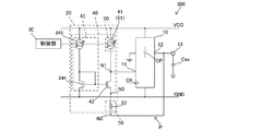
- FIG. 1 is a diagram illustrating a power supply circuit according to the present embodiment.
- the power supply circuit 100 according to the present embodiment is a current feedback charge pump circuit that generates an output voltage obtained by stepping down an input voltage, and includes a charge pump circuit 10, a feedback circuit 20, and a control unit 30.
- the feedback circuit 20 forms a feedback path P that connects the output unit 12 of the charge pump circuit 10 and the input unit 11 of the charge pump circuit 10.
- the feedback path P of the feedback circuit 20 includes a first node N1 connected to the input unit 11 of the charge pump circuit 10, a third node N3 connected to the output unit 12 of the charge pump circuit 10, and a first node N1. And a second node N2 provided between the third nodes N3.
- the charge pump circuit 10 includes a charge / discharge voltage used for charging / discharging the capacitor CP that holds the charge pump charge, an oscillation signal for switching on / off of a switch element that switches a charge / discharge direction to the capacitor CP, And outputs a voltage corresponding to the charge / discharge voltage and the oscillation signal.
- the charge / discharge voltage and the oscillation signal input to the charge pump circuit 10 are collectively referred to as a CP control signal.
- the charge pump circuit 10 is appropriately supplied with a reference voltage used for charging / discharging the capacitor CP from an arbitrary bias source as necessary.
- the charge / discharge voltage is input from the feedback circuit 20 and the clock signal CK supplied from the outside is input as an oscillation signal.
- the charge pump circuit 10 outputs a voltage corresponding to the CP control signal to the output pad 13 as the output voltage Vout.
- An external capacitor Cex is connected to the output pad 13.
- the feedback circuit 20 autonomously adjusts the voltage relationship of each node from the first node N1> the second node N2 (constant voltage)> the third node N3.
- the feedback circuit 20 autonomously adjusts the output voltage Vout between the first node N1 and the second node N2 so that the second voltage V2 of the second node N2 becomes a constant voltage (for example, 0 V). It has a working voltage regulator circuit 40.
- the voltage adjustment circuit 40 includes, for example, a current source 41, a MOS transistor element 42, and a bias circuit 43.
- the current source 41 is provided between the first node N1 and the high potential side constant voltage source VDD, and generates a current I flowing from the high potential side constant voltage source VDD toward the first node N1.
- the value of the current I flowing through the current source 41 is controlled by the control unit 30.
- the MOS transistor element 42 is configured by connecting a source / drain connection to a feedback path P between the first node N1 and the second node N2. That is, the first node N1 and the second node N2 are connected via the MOS transistor element.
- the MOS transistor element 42 is interposed between the first node N1 and the second node N2 of the feedback path P with the drain facing the first node N1 and the source facing the second node N2.
- the bias circuit 43 applies an ON voltage Von to the gate which is a control terminal of the MOS transistor element 42.
- the on-voltage Von is higher than the second voltage V2 of the second node N2 by the gate-source voltage Vgs, where the gate-source voltage of the MOS transistor element 42 is Vgs.
- the source voltage is controlled to the second voltage V2.
- the current I generated by the current source 41 flows from the first node N1 to the second node N2 via the MOS transistor element 42.
- a voltage VDS is generated between the source and drain of the MOS transistor element 42. That is, the first voltage V1 at the first node N1 is higher than the second voltage V2 at the second node N2 by the voltage VDS.
- a potential difference forming circuit 50 is provided between the second node N2 and the third node N3.
- the potential difference forming circuit 50 forms a potential difference in which the second voltage V2 at the second node N2, which is a constant voltage, is used as a reference voltage, and the third voltage V3 at the third node N3 is lower than the second voltage V2.
- the potential difference forming circuit 50 can be configured by, for example, a current source 51 (common to the current source 41 in the present embodiment) and a resistor 52 (hereinafter, the resistance value is ZF).
- the feedback path P between the second node N2 and the third node N3 is connected via a resistor 52.
- the current I generated by the current source 51 flows from the second node N2 to the third node N3 via the resistor 52.
- a voltage VZF corresponding to the current I and the resistance value ZF is generated in the resistor 52 as shown in the following formula (1).
- the third voltage V3 at the third node N3 is lower by the voltage VZF than the second voltage V2 at the second node N2.
- the control unit 30 controls the value of the current I generated by the current source 41 (current source 51).
- the current source 41 (current source 51) and the control unit 30 are configured by a current mirror circuit, for example.
- the power supply circuit 100 described above does not use an operational amplifier, it can operate at a low voltage, and can realize a stability and a circuit area smaller than the conventional one. Further, since the power supply circuit 100 does not use a voltage dividing circuit, there is no increase in circuit area due to the level shifter.
- the conventional voltage feedback charge pump circuit using an operational amplifier is a three-pole system, and since there is a strong dependency between the second and third poles, the first and second poles are scaled by performing constant current density scaling. Paul's relationship can be improved, but at that time the relationship between the second and third poles gets worse.
- the current feedback type power supply circuit according to the present embodiment is a two-pole system, and the relationship between the first pole and the second pole can be improved by performing constant scaling of current density in consideration of only the second pole.
- current scaling can be performed while the gain band product is kept constant, and the second pole P2 can be shifted to the high frequency side, so that there is no tradeoff with the phase margin.
- Current scaling can be performed.
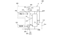
- FIG. 2 is a diagram for explaining the power supply circuit according to the present embodiment.
- the power supply circuit 200 according to this embodiment is a current feedback charge pump circuit that generates an output voltage obtained by boosting an input voltage, and includes a charge pump circuit 210, a feedback circuit 220, and a control unit 230.
- the feedback circuit 220 forms a feedback path P that connects between the output unit 212 of the charge pump circuit 210 and the input unit 211 of the charge pump circuit 210.
- the feedback path P of the feedback circuit 220 includes a first node N1 connected to the input unit 211 of the charge pump circuit 210, a third node N3 connected to the output unit 212 of the charge pump circuit 210, and the first node N1. And a second node N2 provided between the third nodes N3.
- the charge pump circuit 210 includes a charge / discharge voltage used for charging / discharging the capacitor CP that holds the charge pump charge, and an oscillation signal for switching on / off of a switch element that switches a charge / discharge direction to the capacitor CP, And outputs a voltage corresponding to the charge / discharge voltage and the oscillation signal.
- the charge / discharge voltage and the oscillation signal input to the charge pump circuit 210 are collectively referred to as a CP control signal.
- the charge pump circuit 210 is appropriately supplied with a reference voltage used for charging and discharging the capacitor CP from an arbitrary bias source as necessary.
- the charge / discharge voltage is input from the feedback circuit 220, and the clock signal CK supplied from the outside is input as an oscillation signal.
- the charge pump circuit 210 outputs a voltage corresponding to the CP control signal to the output pad 213 as the output voltage Vout.
- An external capacitor Cex is connected to the output pad 213.
- the feedback circuit 220 autonomously adjusts the voltage relationship of each node from the third node N3> the second node N2 (constant voltage)> the first node N1.
- the feedback circuit 220 outputs the output voltage Vout between the first node N1 and the second node N2 so that the second voltage V2 of the second node N2 becomes a constant voltage (for example, the potential of the high potential side constant voltage source VDD).
- a voltage adjustment circuit 240 that operates to adjust autonomously is included.
- the voltage adjustment circuit 240 includes, for example, a current source 241, a MOS transistor element 242, and a bias circuit 243.
- the current source 241 is provided between the first node N1 and the low potential side constant voltage source GND, and generates a current I flowing from the first node N1 toward the low potential side constant voltage source GND.
- the value of the current I flowing through the current source 241 is controlled by the control unit 230.
- the MOS transistor element 242 is configured by connecting a source / drain connection to a feedback path P between the first node N1 and the second node N2. That is, the first node N 1 and the second node N 2 are connected via the MOS transistor element 242.
- the MOS transistor element 242 is interposed between the first node N1 and the second node N2 of the feedback path P with the drain facing the first node N1 and the source facing the second node N2.
- the bias circuit 243 applies an on voltage Von to the gate which is the control terminal of the MOS transistor element 242.
- the on-voltage Von is lower than the second voltage V2 of the second node N2 by the gate-source voltage Vgs, assuming that the gate-source voltage of the MOS transistor element 242 is Vgs.
- the source voltage of the MOS transistor element 242 to which the voltage of (V2-Vgs) is applied to the gate is controlled to the second voltage V2.
- the current I generated by the current source 241 reaches the current source 241 from the second node N2 through the MOS transistor element 242 and the first node N1.
- a voltage VDS is generated between the source and drain of the MOS transistor element 242. That is, the second voltage V2 at the second node N2 is higher than the first voltage V1 at the first node N1 by the voltage VDS.
- a potential difference forming circuit 250 is provided between the second node N2 and the third node N3.
- the potential difference forming circuit 250 forms a potential difference in which the second voltage V2 at the second node N2 that is a constant voltage is used as a reference voltage, and the third voltage V3 at the third node N3 is higher than the second voltage V2.
- the potential difference forming circuit 250 can be configured by, for example, a current source 251 (common to the current source 241 in this embodiment) and a resistor 252 (hereinafter, the resistance value is ZF).
- the feedback path P between the second node N2 and the third node N3 is connected via a resistor 252.
- the current I generated by the current source 251 flows from the third node N3 to the second node N2 via the resistor 252.
- a voltage VZF corresponding to the current I and the resistance value ZF is generated in the resistor 252 as shown in the following formula (2).
- the third voltage V3 at the third node N3 is higher than the second voltage V2 at the second node N2 by the voltage VZF.
- the control unit 230 controls the value of the current I generated by the current source 241 (current source 251).
- the current source 241 (current source 251) and the control unit 230 are configured by a current mirror circuit, for example.
- FIG. 3 is a diagram illustrating the power supply circuit according to the present embodiment.
- the power supply circuit 300 according to the present embodiment is an example of a configuration in which the bias circuit 43 and the current source 41 (current source 51) of the power supply circuit 100 according to the first embodiment are specifically realized by a current mirror circuit.
- symbol as 1st Embodiment is attached
- the gate of the MOS transistor element 42 is connected to the gate of the MOS transistor element 344 having the same characteristics as the MOS transistor element 42, and the gate and drain of the MOS transistor element 344 are short-circuited.
- This is a basic current mirror circuit configuration in which the source of the element 344 is connected to the low potential side constant voltage source GND, and the current source 345 connects the drain of the MOS transistor element 344 and the high potential side constant voltage source VDD.
- the configuration of the current mirror circuit provided in the power supply circuit 300 according to the present embodiment is not limited to the basic configuration and can be variously changed.
- the current source 345 is configured such that the current value is controlled by the same control signal from the same control unit 30 so as to flow the same current I as that of the current source 41 (current source 51). That is, by changing the control signal of the control unit 30, the values of the current I of both the current source 345 and the current source 41 (current source 51) can be easily adjusted.
- the bias circuit 343 can be realized with a simple configuration.
- FIG. 4 is a diagram for explaining the power supply circuit according to the present embodiment.
- the power supply circuit 400 according to the present embodiment is an example of a configuration in which the bias circuit 243 and the current source 241 (current source 251) of the power supply circuit 200 according to the second embodiment are specifically realized by a current mirror circuit.
- symbol as 2nd Embodiment is attached
- the gate of the MOS transistor element 242 is connected to the gate of the MOS transistor element 444 having the same characteristics as the MOS transistor element 242 and the gate and drain of the MOS transistor element 444 are short-circuited.
- This is a basic current mirror circuit configuration in which the source of the element 444 is connected to the high potential side constant voltage source VDD, and the drain of the MOS transistor element 444 and the high potential side constant voltage source VDD are connected by the current source 445.
- the configuration of the current mirror circuit provided in the power supply circuit 400 according to the present embodiment is not limited to the basic configuration and can be variously changed.
- the current source 445 is configured such that the current value is controlled by the same control signal from the same control unit 230 so as to flow the same current I as the current source 241 (current source 251). That is, by changing the control signal of the control unit 230, the values of the current I of both the current source 445 and the current source 241 (current source 251) can be easily adjusted.
- the bias circuit 243 can be realized with a simple configuration.
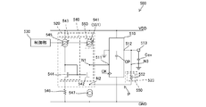
- FIG. 5 is a diagram for explaining the power supply circuit according to the present embodiment.
- the power supply circuit 500 according to the present embodiment is a current feedback charge pump circuit that generates an output voltage obtained by boosting an input voltage, and includes a charge pump circuit 510, a feedback circuit 520, and a control unit 530.
- the feedback circuit 520 forms a feedback path P that connects between the output unit 512 of the charge pump circuit 510 and the input unit 511 of the charge pump circuit 510.
- the feedback path P of the feedback circuit 520 includes a first node N1 connected to the input unit 511 of the charge pump circuit 510, a third node N3 connected to the output unit 512 of the charge pump circuit 510, and the first node N1. And a second node N2 provided between the third nodes N3.
- the charge pump circuit 510 includes a charge / discharge voltage used for charging / discharging the capacitor CP that holds the charge pump charge, an oscillation signal for switching on / off of a switch element that switches a charge / discharge direction to the capacitor CP, And outputs a voltage corresponding to the charge / discharge voltage and the oscillation signal.
- the charge pump circuit 510 is appropriately supplied with a reference voltage used for charging and discharging the capacitor CP from an arbitrary bias source as necessary.
- a charge / discharge voltage is input from the feedback circuit 520, and a clock signal CK supplied from the outside is input as an oscillation signal.
- the charge / discharge voltage and the oscillation signal input to the charge pump circuit 510 are collectively referred to as a CP control signal.
- the charge pump circuit 510 outputs a voltage corresponding to the CP control signal to the output pad 513 as the output voltage Vout.
- An external capacitor Cex is connected to the output pad 513.
- the feedback circuit 520 autonomously adjusts the voltage relationship of each node from the third node N3> the first node N1> the second node N2 (constant voltage).
- the feedback circuit 520 outputs a voltage between the first node N1 and the second node N2 so that the second voltage V2 of the second node N2 becomes a constant voltage (voltage generated when a current I flows through a resistor 546 described later).
- a voltage adjustment circuit 540 that operates to adjust Vout autonomously is included.
- the voltage adjustment circuit 540 includes, for example, a current source 541, a MOS transistor element 542, and a bias circuit 543.
- the current source 541 is provided between the first node N1 and the high potential side constant voltage source VDD, and generates a current I flowing from the high potential side constant voltage source VDD toward the first node N1.
- the value of the current I flowing through the current source 541 is controlled by the control unit 530.
- the feedback path P between the first node N1 and the second node N2 is configured via the source / drain connection of the MOS transistor element 542, and is connected via the MOS transistor element 542.
- the MOS transistor element 542 is interposed between the first node N1 and the second node N2 of the feedback path P with the drain facing the first node N1 and the source facing the second node N2.
- the bias circuit 543 applies the ON voltage Von to the gate which is the control terminal of the MOS transistor element 542.
- the on-voltage Von is higher than the second voltage V2 of the second node N2 by the gate-source voltage Vgs, where Vgs is the gate-source voltage of the MOS transistor element 542.
- Vgs is the gate-source voltage of the MOS transistor element 542.
- the bias circuit 543 has a current mirror circuit configuration.
- the bias circuit 543 having the configuration of a current mirror circuit connects the gate of the MOS transistor element 544 having the same characteristics as the MOS transistor element 542 to the gate of the MOS transistor element 542, and short-circuits the gate and drain of the MOS transistor element 544.
- the source of the MOS transistor element 544 is connected to the low potential side constant voltage source GND via the resistor 546, and the current source 545 connects the drain of the MOS transistor element 544 and the high potential side constant voltage source VDD.
- This is a configuration of a current mirror circuit. Note that the configuration of the current mirror circuit is not limited to the basic configuration.
- the current source 545 is configured such that the current value is controlled by the same control signal from the same control unit 530 in order to flow the same current I as the current source 541 (current source 551). That is, by changing the control signal of the control unit 530, the values of the current I of both the current source 545 and the current source 541 (current source 551) can be easily adjusted.
- the bias circuit 543 can be realized with a simple configuration.
- the current I generated by the current source 541 flows from the first node N1 to the second node N2 via the MOS transistor element 542.
- a voltage VDS is generated between the source and drain of the MOS transistor element 542. That is, the first voltage V1 at the first node N1 is higher than the second voltage V2 at the second node N2 by the voltage VDS.
- the second node N2 is connected to the low potential side constant voltage GND through a current source 547 as a second current source.
- the current source 547 generates a current I ′ that flows from the second node N2 to the low potential side constant voltage GND. Therefore, the current I that the current source 541 flows to the MOS transistor element 542 through the first node N1 flows to the low potential side constant voltage GND through the current source 547.
- a potential difference forming circuit 550 is provided between the second node N2 and the third node N3.
- the potential difference forming circuit 550 forms a potential difference in which the second voltage V2 at the second node N2, which is a constant voltage, is used as a reference voltage, and the third voltage V3 at the third node N3 is higher than the second voltage V2.
- the potential difference between the second node N2 and the third node N3 formed by the potential difference forming circuit 550 is made larger than the potential difference between the second node N2 and the first node N1 formed by the MOS transistor element 542.
- the potential difference forming circuit 550 can be configured by, for example, a current source 551 (common to the current source 541 in this embodiment) and a resistor 552 (hereinafter, the resistance value is ZF).
- the feedback path P between the second node N2 and the third node N3 is connected via a resistor 552.
- a voltage VZF corresponding to the current (I-I ′) and the resistance value ZF is generated in the resistor 552 as shown in the following formula (3).
- the third voltage V3 at the third node N3 is higher than the second voltage V2 at the second node N2 by the voltage VZF.
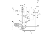
- FIG. 6 is a diagram for explaining the power supply circuit according to the present embodiment.
- the power supply circuit 600 according to the present embodiment is a current feedback charge pump circuit that generates an output voltage obtained by boosting an input voltage, and includes a charge pump circuit 610, a feedback circuit 620, and a control unit 630.
- the feedback circuit 620 forms a feedback path P that connects between the output unit 612 of the charge pump circuit 610 and the input unit 611 of the charge pump circuit 610.
- the feedback path P of the feedback circuit 620 includes a first node N1 connected to the input unit 611 of the charge pump circuit 610, a third node N3 connected to the output unit 612 of the charge pump circuit 610, and the first node N1. And a second node N2 provided between the third nodes N3.
- the charge pump circuit 610 includes a charge / discharge voltage used for charging / discharging the capacitor CP that holds the charge pump charge, and an oscillation signal for switching on / off of a switch element that switches a charge / discharge direction to the capacitor CP, And outputs a voltage corresponding to the charge / discharge voltage and the oscillation signal.
- the charge / discharge voltage and the oscillation signal input to the charge pump circuit 610 are collectively referred to as a CP control signal.
- the charge pump circuit 610 is appropriately supplied with a reference voltage used for charging and discharging the capacitor CP from an arbitrary bias source as necessary.
- the charge / discharge voltage is input from the feedback circuit 620, and the clock signal CK supplied from the outside is input as an oscillation signal.
- the charge pump circuit 610 outputs a voltage corresponding to the CP control signal to the output pad 613 as the output voltage Vout.
- An external capacitor Cex is connected to the output pad 613.
- the feedback circuit 620 autonomously adjusts the voltage relationship of each node from second node N2 (constant voltage)> first node N1> third node N3.
- the feedback circuit 620 outputs a voltage between the first node N1 and the second node N2 so that the second voltage V2 of the second node N2 becomes a constant voltage (a voltage generated when a current I flows through a resistor 646 described later).
- a voltage adjustment circuit 640 that operates to adjust Vout autonomously is included.
- the voltage adjustment circuit 640 includes, for example, a current source 641, a MOS transistor element 642, and a bias circuit 643.
- the feedback path P between the first node N1 and the second node N2 is configured via the source / drain connection of the MOS transistor element 642, and is connected via the MOS transistor element 642.
- the MOS transistor element 642 is interposed between the first node N1 and the second node N2 of the feedback path P with the source facing the second node N2 and the drain facing the first node N1.
- the bias circuit 643 applies the ON voltage Von to the gate which is the control terminal of the MOS transistor element 642.
- the on-voltage Von is lower than the second voltage V2 of the second node N2 by the gate-source voltage Vgs, where the gate-source voltage of the MOS transistor element 642 is Vgs.
- the source voltage of the MOS transistor element 642 to which the voltage of (V2 ⁇ Vgs) is applied to the gate is controlled to the second voltage V2.
- the current values of the current source 645 and the current source 641 are controlled by the same control unit 630. That is, the value of the current I flowing through the current source 645 and the current source 641 (current source 651) is adjusted to the same value under the control of the control unit 630.
- the current I generated by the current source 641 flows from the second node N2 to the first node N1 via the MOS transistor element 642.
- a voltage VDS is generated between the source and drain of the MOS transistor element 642. That is, the first voltage V1 at the first node N1 is lower than the second voltage V2 at the second node N2 by the voltage VDS.
- the second node N2 is connected to the high potential side constant voltage source VDD via a current source 647 as a second current source.
- the current source 647 generates a current I ′ that flows from the high potential side constant voltage source VDD to the second node N2. Therefore, the current I that the current source 641 flows from the second node N2 through the MOS transistor element 642 to the first node N1 constitutes a part of the current I ′.
- a potential difference forming circuit 650 is provided between the second node N2 and the third node N3.
- the potential difference forming circuit 650 forms a potential difference in which the second voltage V2 at the second node N2, which is a constant voltage, is used as a reference voltage, and the third voltage V3 at the third node N3 is lower than the second voltage V2.
- a voltage VZF corresponding to the current (I′-I) and the resistance value ZF is generated in the resistor 652 as shown in the following formula (4).
- the third voltage V3 at the third node N3 is lower by the voltage VZF than the second voltage V2 at the second node N2.
- FIG. 7 is a diagram for explaining the power supply circuit according to the present embodiment.
- the power supply circuit 700 according to the present embodiment is configured to input the first voltage V1 of the first node N1 to the charge pump circuit 10 via the buffer 760.
- the buffer 760 may be provided in the power supply circuit 100 according to the first embodiment, the buffer 760 may be provided in the power supply circuits according to the second to sixth embodiments. Further, the buffer 760 may be built in the charge pump circuit 10.
- FIG. 8 is a diagram for explaining the power supply circuit according to the present embodiment.
- the power supply circuit 800 includes a current source 870 as a third current source on a line that supplies the low-potential-side constant voltage GND to the buffer 760 provided in the charge pump circuit 10 according to the seventh embodiment.
- the first voltage V1 of the first node N1 is used as a control signal for changing the current value of the current source 870.
- the buffer 760 receives, for example, an external clock signal CK.
- the load of the charge pump circuit 10 is light and the idle current to be supplied to the charge pump circuit 10 is small.
- the current flowing through the buffer 760 is reduced to save power, and when the load of the charge pump circuit 10 is heavy and the drive capability of the charge pump circuit 10 needs to be increased, the current flowing through the buffer 760 is increased.
- the power supply circuit 800 that automatically adjusts the supply current to the charge pump circuit 10 in accordance with the load state is realized.
- FIG. 9 is a diagram for explaining the power supply circuit according to the present embodiment.
- the power supply circuit 900 according to the present embodiment is configured to supply the charge pump circuit 10 with an oscillation signal CK output from an oscillator 980 whose presence or absence of oscillation is controlled by the first voltage V1 of the first node N1.
- FIG. 9 shows an example in which the power supply circuit 100 according to the first embodiment is provided with the oscillator 980
- the power supply circuits according to the second to sixth embodiments may be provided with the oscillator 980.
- the oscillator 980 may be built in the charge pump circuit 10.
- the oscillator 980 supplies the oscillation signal CK to the charge pump circuit 10 when the first voltage V1 of the first node N1 becomes equal to or higher than a certain threshold value, and oscillates when the first voltage V1 of the first node N1 is less than the certain threshold value.
- the output of the signal CK is stopped.
- the oscillation signal CK supplied from the oscillator 980 to the charge pump circuit 10 is used to switch on / off the switch element that switches the charge / discharge direction to the capacitor CP.
- the power supply circuit 900 configured as described above is configured to switch the switch group only when necessary, to charge / discharge the capacitor CP, and to charge / discharge from the charge pump circuit 10 to the external capacitor Cex. Therefore, when the load of the charge pump circuit 10 is small, a power saving operation can be effectively realized.
- FIG. 10 is a diagram illustrating the power supply circuit according to the present embodiment.
- the power supply circuit 1000 according to the present embodiment has a configuration in which a filter 1090 is provided on a control line in which the control unit 30 controls the current values of the current source 41 (current source 51) and the current source 345.
- FIG. 10 shows an example in which the filter 1090 is provided in the power supply circuit 300 according to the third embodiment, but the current sources (41 (51), 241 (251), 445, 545, other embodiments) are shown.
- a similar filter may be provided for the control lines for controlling the current values of 547, 641 (651), 645, 647).
- the filter 1090 may be a smoothing filter that removes fluctuations in the control signal input to the current source, and it is sufficient if the fluctuations can be made sufficiently smaller than the bandwidth of the feedback circuit.
- a primary RC filter can be used.
- the present technology is not limited to the above-described embodiments, and the configurations disclosed in the above-described embodiments are replaced with each other or the combination thereof is changed, disclosed in the known technology, and in the above-described embodiments. A configuration in which each configuration is mutually replaced or a combination is changed is also included.
- the technical scope of the present technology is not limited to the above-described embodiment, but extends to the matters described in the claims and equivalents thereof.
- a charge pump circuit A feedback circuit for feeding back the output of the charge pump circuit to the input;
- a first current source for supplying a constant current to the feedback circuit;
- a MOS transistor element interposed in the middle of the feedback circuit;
- a resistance element interposed in a position closer to the output of the charge pump circuit than the MOS transistor element in the feedback circuit;
- a bias circuit for applying a constant voltage to the control terminal of the MOS transistor element;
- a controller that controls the value of a constant current that the first current source passes through the feedback circuit;
- a power supply circuit comprising:
- the constant voltage applied by the bias circuit is higher than the reference voltage by an amount corresponding to the gate-source voltage of the MOS transistor element.
- a node between the MOS transistor element and the resistance element of the feedback circuit is connected to a constant voltage source by a second current source;
- the power supply circuit according to (2) is
- the constant voltage applied by the bias circuit is lower than the reference voltage by the gate-source voltage of the MOS transistor element.
- the power supply circuit according to any one of (1) to (3).
- the feedback circuit is connected to the input of the charge pump circuit through a buffer.
- the power supply circuit according to any one of (1) to (4).
- the output of the buffer is input to the input of the charge pump circuit,
- the buffer is supplied with current by a third current source,
- the third current source is any one of (1) to (6), wherein a current value is controlled by a voltage of a node which is a terminal opposite to the resistance element of the MOS transistor element of the feedback circuit.
- An oscillator whose oscillation is controlled by a voltage of a node which is a terminal opposite to the resistance element of the MOS transistor element of the feedback circuit; The output of the oscillator is input to the charge pump circuit.
- the power supply circuit according to any one of (1) to (4).
- a control signal for controlling the current value of the first current source is input through a smoothing filter.
- the power supply circuit according to any one of (1) to (4).
- SYMBOLS 10 Charge pump circuit, 11 ... Input part, 12 ... Output part, 13 ... Output pad, 20 ... Feedback circuit, 30 ... Control part, 41 ... Current source, 42 ... MOS transistor element, 43 ... Bias circuit, 40 ... Voltage Adjustment circuit 51 ... Current source 52 ... Resistance 50 ... Potential difference forming circuit 100 ... Power supply circuit 200 ... Power supply circuit 210 ... Charge pump circuit 211 ... Input unit 212 ... Output unit 213 ... Output pad 220 DESCRIPTION OF SYMBOLS ... Feedback circuit, 230 ... Control part, 241 ... Current source, 242 ... MOS transistor element, 243 ... Bias circuit, 240 ...
- Voltage adjustment circuit 251 ... Current source, 252 ... Resistance, 250 ... Potential difference formation circuit, 300 ... Power supply circuit 343: Bias circuit, 344: MOS transistor element, 345: Current source, 400: Power supply circuit, 444 ... MOS transistor element 445 ... Current source, 500 ... Power supply circuit, 510 ... Charge pump circuit, 511 ... Input unit, 512 ... Output unit, 513 ... Output pad, 520 ... Feedback circuit, 530 ... Control unit, 541 ... Current source, 542 ... MOS transistor Element, 543 ... Bias circuit, 544 ... MOS transistor element, 545 ... Current source, 546 ... Resistance, 547 ... Current source, 540 ...
- Voltage adjustment circuit 551 ... Current source, 552 ... Resistance, 550 ... Potential difference forming circuit, 600 ... Power supply circuit, 610 ... charge pump circuit, 611 ... input unit, 612 ... output unit, 613 ... output pad, 620 ... feedback circuit, 630 ... control unit, 641 ... current source, 642 ... MOS transistor element, 643 ... bias circuit, 644 ... MOS transistor element, 645 ... current source, 646 ... resistor, 647 ... current source, 640 ... voltage Adjusting circuit, 651 ... current source, 652 ... resistor, 650 ... potential difference forming circuit, 700 ... power supply circuit, 760 ... buffer, 800 ... power supply circuit, 870 ... current source, 900 ... power supply circuit, 980 ... oscillator, 1000 ... power supply circuit 1090: Filter, N1: First node, N2: Second node, N3: Third node, P: Feedback path
Landscapes
- Engineering & Computer Science (AREA)
- Power Engineering (AREA)
- Dc-Dc Converters (AREA)
- Amplifiers (AREA)
Abstract
Description
図1は、本実施形態に係る電源回路を説明する図である。本実施形態に係る電源回路100は、入力電圧を降圧した出力電圧を生成する電流帰還型のチャージポンプ回路であり、チャージポンプ回路10、帰還回路20及び制御部30を備える。

図2は、本実施形態に係る電源回路を説明する図である。本実施形態に係る電源回路200は、入力電圧を昇圧した出力電圧を生成する電流帰還型のチャージポンプ回路であり、チャージポンプ回路210、帰還回路220及び制御部230を備える。

図3は、本実施形態に係る電源回路を説明する図である。
図4は、本実施形態に係る電源回路を説明する図である。
図5は、本実施形態に係る電源回路を説明する図である。本実施形態に係る電源回路500は、入力電圧を昇圧した出力電圧を生成する電流帰還型のチャージポンプ回路であり、チャージポンプ回路510、帰還回路520及び制御部530を備える。
続される。

図6は、本実施形態に係る電源回路を説明する図である。本実施形態に係る電源回路600は、入力電圧を昇圧した出力電圧を生成する電流帰還型のチャージポンプ回路であり、チャージポンプ回路610、帰還回路620及び制御部630を備える。

図7は、本実施形態に係る電源回路を説明する図である。本実施形態に係る電源回路700は、第1ノードN1の第1電圧V1をバッファ760を介してチャージポンプ回路10へ入力する構成である。
図8は、本実施形態に係る電源回路を説明する図である。本実施形態に係る電源回路800は、上述した第7実施形態に係るチャージポンプ回路10に設けたバッファ760に低電位側定電圧GNDを供給するライン上に第三電流源としての電流源870を介設し、第1ノードN1の第1電圧V1を電流源870の電流値を可変する制御信号として用いる構成である。バッファ760は、例えば外部のクロック信号CKを入力とする。
図9は、本実施形態に係る電源回路を説明する図である。本実施形態に係る電源回路900は、第1ノードN1の第1電圧V1により発振の有無を制御される発振器980の出力する発振信号CKをチャージポンプ回路10へ供給する構成である。
図10は、本実施形態に係る電源回路を説明する図である。本実施形態に係る電源回路1000は、電流源41(電流源51)及び電流源345の電流値を制御部30が制御する制御ライン上にフィルター1090を介設した構成である。
チャージポンプ回路と、
前記チャージポンプ回路の出力を入力へフィードバックする帰還回路と、
前記帰還回路に定電流を流す第一電流源と、
前記帰還回路の途中に介設されるMOSトランジスタ素子と、
前記帰還回路において前記MOSトランジスタ素子よりも前記チャージポンプ回路の出力寄りの位置に介設される抵抗素子と、
前記MOSトランジスタ素子の制御端子に定電圧を印加するバイアス回路と、
前記第一電流源が前記帰還回路に流す定電流の値を制御する制御部と、
を備える電源回路。
前記バイアス回路が印加する定電圧は、基準電圧に比べて前記MOSトランジスタ素子のゲート・ソース間電圧相当だけ高電圧である、
前記(1)に記載の電源回路。
前記帰還回路の前記MOSトランジスタ素子と前記抵抗素子の間のノードを、第二電流源により定電圧源に対して接続した、
前記(2)に記載の電源回路。
前記バイアス回路が印加する定電圧は、前記MOSトランジスタ素子のゲート・ソース間電圧相当だけ基準電圧より低電圧である、
前記(1)~前記(3)の何れか1つに記載の電源回路。
前記(1)~前記(4)の何れか1つに記載の電源回路。
前記チャージポンプ回路の入力にはバッファの出力が入力され、
前記バッファには第三電流源により電流供給され、
前記第三電流源は、前記帰還回路の前記MOSトランジスタ素子の前記抵抗素子と反対側の端子であるノードの電圧で電流値を制御される
前記(1)~前記(6)の何れか1つに記載の電源回路。
前記帰還回路の前記MOSトランジスタ素子の前記抵抗素子と反対側の端子であるノードの電圧で発振を制御される発振器を更に備え、
前記発振器の出力が、前記チャージポンプ回路に入力される、
前記(1)~前記(4)の何れか1つに記載の電源回路。
前記第一電流源の電流値を制御する制御信号は、平滑化フィルターを介して入力される、
前記(1)~前記(4)の何れか1つに記載の電源回路。
Claims (8)
- チャージポンプ回路と、
前記チャージポンプ回路の出力を入力へフィードバックする帰還回路と、
前記帰還回路に定電流を流す第一電流源と、
前記帰還回路の途中に介設されるMOSトランジスタ素子と、
前記帰還回路において前記MOSトランジスタ素子よりも前記チャージポンプ回路の出力寄りの位置に介設される抵抗素子と、
前記MOSトランジスタ素子の制御端子に定電圧を印加するバイアス回路と、
前記第一電流源が前記帰還回路に流す定電流の値を制御する制御部と、
を備える電源回路。 - 前記バイアス回路が印加する定電圧は、基準電圧に比べて前記MOSトランジスタ素子のゲート・ソース間電圧相当だけ高電圧である、
請求項1に記載の電源回路。 - 前記帰還回路の前記MOSトランジスタ素子と前記抵抗素子の間のノードを、第二電流源により定電圧源に対して接続した、
請求項2に記載の電源回路。 - 前記バイアス回路が印加する定電圧は、前記MOSトランジスタ素子のゲート・ソース間電圧相当だけ基準電圧より低電圧である、
請求項1に記載の電源回路。 - 前記帰還回路は、バッファを介して前記チャージポンプ回路の入力に接続されている、
請求項1に記載の電源回路。 - 前記チャージポンプ回路の入力にはバッファの出力が入力され、
前記バッファには第三電流源により電流供給され、
前記第三電流源は、前記帰還回路の前記MOSトランジスタ素子の前記抵抗素子と反対側の端子であるノードの電圧で電流値を制御される
請求項1に記載の電源回路。 - 前記帰還回路の前記MOSトランジスタ素子の前記抵抗素子と反対側の端子であるノードの電圧で発振を制御される発振器を更に備え、
前記発振器の出力が、前記チャージポンプ回路に入力される、
請求項1に記載の電源回路。 - 前記第一電流源の電流値を制御する制御信号は、平滑化フィルターを介して入力される、
請求項1に記載の電源回路。
Priority Applications (3)
| Application Number | Priority Date | Filing Date | Title |
|---|---|---|---|
| KR1020197030758A KR102512576B1 (ko) | 2017-05-09 | 2018-04-24 | 전원 회로 |
| US16/609,811 US11271476B2 (en) | 2017-05-09 | 2018-04-24 | Power supply circuit comprising a charge pump circuit and a feedback circuit for the charge pump circuit |
| CN201880029239.8A CN110622403B (zh) | 2017-05-09 | 2018-04-24 | 电源电路 |
Applications Claiming Priority (2)
| Application Number | Priority Date | Filing Date | Title |
|---|---|---|---|
| JP2017093425 | 2017-05-09 | ||
| JP2017-093425 | 2017-05-09 |
Publications (1)
| Publication Number | Publication Date |
|---|---|
| WO2018207614A1 true WO2018207614A1 (ja) | 2018-11-15 |
Family
ID=64104482
Family Applications (1)
| Application Number | Title | Priority Date | Filing Date |
|---|---|---|---|
| PCT/JP2018/016607 Ceased WO2018207614A1 (ja) | 2017-05-09 | 2018-04-24 | 電源回路 |
Country Status (4)
| Country | Link |
|---|---|
| US (1) | US11271476B2 (ja) |
| KR (1) | KR102512576B1 (ja) |
| CN (1) | CN110622403B (ja) |
| WO (1) | WO2018207614A1 (ja) |
Families Citing this family (1)
| Publication number | Priority date | Publication date | Assignee | Title |
|---|---|---|---|---|
| US12040705B2 (en) * | 2021-08-20 | 2024-07-16 | Semiconductor Components Industries, Llc | Self clocked low power doubling charge pump |
Citations (5)
| Publication number | Priority date | Publication date | Assignee | Title |
|---|---|---|---|---|
| JPH07248837A (ja) * | 1994-03-11 | 1995-09-26 | Fuji Film Micro Device Kk | 基準電圧発生回路 |
| JP2003168293A (ja) * | 2001-11-29 | 2003-06-13 | Matsushita Electric Ind Co Ltd | 半導体記憶装置およびその製造方法 |
| US20140028276A1 (en) * | 2012-07-30 | 2014-01-30 | SK Hynix Inc. | Internal voltage generator having immunity to ground bouncing |
| JP2014147044A (ja) * | 2013-01-30 | 2014-08-14 | Toshiba Corp | 半導体集積回路 |
| JP2015171213A (ja) * | 2014-03-06 | 2015-09-28 | ヤマハ株式会社 | 昇圧回路 |
Family Cites Families (8)
| Publication number | Priority date | Publication date | Assignee | Title |
|---|---|---|---|---|
| DE19962523A1 (de) | 1999-12-23 | 2001-08-02 | Texas Instruments Deutschland | Gleichspannungswandler und Verfahren zum Betreiben eines Gleichspannungswandlers |
| US6566847B1 (en) * | 2002-07-29 | 2003-05-20 | Taiwan Semiconductor Manufacturing Company | Low power charge pump regulating circuit |
| JP4666345B2 (ja) * | 2004-11-05 | 2011-04-06 | ローム株式会社 | チャージポンプ回路 |
| JP3904579B2 (ja) * | 2004-12-03 | 2007-04-11 | ローム株式会社 | 電源装置およびそれを用いた発光装置、電子機器 |
| JP4615524B2 (ja) | 2004-12-06 | 2011-01-19 | ローム株式会社 | 昇圧回路及びこれを用いた携帯機器 |
| US8044704B2 (en) * | 2006-07-07 | 2011-10-25 | Semiconductor Components Industries, Llc | Current controller and method therefor |
| CN102158075B (zh) * | 2011-03-16 | 2013-01-30 | 东南大学 | 一种电荷泵锁相环中的电荷泵电路 |
| US9871514B1 (en) | 2016-06-29 | 2018-01-16 | Texas Instruments Incorporated | Methods and apparatus for continuous current limiting for FETS in high inductive load systems |
-
2018
- 2018-04-24 CN CN201880029239.8A patent/CN110622403B/zh active Active
- 2018-04-24 US US16/609,811 patent/US11271476B2/en active Active
- 2018-04-24 KR KR1020197030758A patent/KR102512576B1/ko active Active
- 2018-04-24 WO PCT/JP2018/016607 patent/WO2018207614A1/ja not_active Ceased
Patent Citations (5)
| Publication number | Priority date | Publication date | Assignee | Title |
|---|---|---|---|---|
| JPH07248837A (ja) * | 1994-03-11 | 1995-09-26 | Fuji Film Micro Device Kk | 基準電圧発生回路 |
| JP2003168293A (ja) * | 2001-11-29 | 2003-06-13 | Matsushita Electric Ind Co Ltd | 半導体記憶装置およびその製造方法 |
| US20140028276A1 (en) * | 2012-07-30 | 2014-01-30 | SK Hynix Inc. | Internal voltage generator having immunity to ground bouncing |
| JP2014147044A (ja) * | 2013-01-30 | 2014-08-14 | Toshiba Corp | 半導体集積回路 |
| JP2015171213A (ja) * | 2014-03-06 | 2015-09-28 | ヤマハ株式会社 | 昇圧回路 |
Also Published As
| Publication number | Publication date |
|---|---|
| US11271476B2 (en) | 2022-03-08 |
| US20210281169A1 (en) | 2021-09-09 |
| CN110622403A (zh) | 2019-12-27 |
| CN110622403B (zh) | 2023-01-10 |
| KR102512576B1 (ko) | 2023-03-23 |
| KR20200004293A (ko) | 2020-01-13 |
Similar Documents
| Publication | Publication Date | Title |
|---|---|---|
| US8841893B2 (en) | Dual-loop voltage regulator architecture with high DC accuracy and fast response time | |
| US8575986B2 (en) | Level shift circuit and switching regulator using the same | |
| JP4774247B2 (ja) | 電圧レギュレータ | |
| US8823343B2 (en) | Power amplifying circuit, DC-DC converter, peak holding circuit, and output voltage control circuit including the peak holding circuit | |
| US8866341B2 (en) | Voltage regulator | |
| JP6038516B2 (ja) | ボルテージレギュレータ | |
| US20170279357A1 (en) | Current detection circuit and dcdc converter including the same | |
| JP2009211667A (ja) | 定電圧回路 | |
| CN110858083B (zh) | 恒压电路 | |
| US10298127B2 (en) | Startup clamp circuit for non-complimentary differential pair in DCDC converter system | |
| JP2009116679A (ja) | リニアレギュレータ回路、リニアレギュレーション方法及び半導体装置 | |
| US20120153909A1 (en) | Hybrid fast-slow passgate control methods for voltage regulators employing high speed comparators | |
| JP2017126259A (ja) | 電源装置 | |
| CN107526385A (zh) | 线性电压调节器 | |
| JP4032066B2 (ja) | 半導体集積回路 | |
| JP4017850B2 (ja) | 電源回路 | |
| JP2006203987A (ja) | スイッチング・レギュレータ回路 | |
| JP2010141589A (ja) | 差動増幅回路 | |
| WO2018207614A1 (ja) | 電源回路 | |
| US7514972B2 (en) | Differential charge pump with open loop common mode | |
| JP2020136895A (ja) | 駆動回路 | |
| JP2007053746A (ja) | 集積回路 | |
| JP4175303B2 (ja) | 電力変換回路および電力変換方法 | |
| US20100033260A1 (en) | Oscillation circuit | |
| JP4211369B2 (ja) | Agc回路 |
Legal Events
| Date | Code | Title | Description |
|---|---|---|---|
| 121 | Ep: the epo has been informed by wipo that ep was designated in this application |
Ref document number: 18797546 Country of ref document: EP Kind code of ref document: A1 |
|
| ENP | Entry into the national phase |
Ref document number: 20197030758 Country of ref document: KR Kind code of ref document: A |
|
| NENP | Non-entry into the national phase |
Ref country code: DE |
|
| 122 | Ep: pct application non-entry in european phase |
Ref document number: 18797546 Country of ref document: EP Kind code of ref document: A1 |
|
| NENP | Non-entry into the national phase |
Ref country code: JP |