WO2018207600A1 - Module de circuit - Google Patents
Module de circuit Download PDFInfo
- Publication number
- WO2018207600A1 WO2018207600A1 PCT/JP2018/016409 JP2018016409W WO2018207600A1 WO 2018207600 A1 WO2018207600 A1 WO 2018207600A1 JP 2018016409 W JP2018016409 W JP 2018016409W WO 2018207600 A1 WO2018207600 A1 WO 2018207600A1
- Authority
- WO
- WIPO (PCT)
- Prior art keywords
- main surface
- electronic component
- circuit module
- center
- heat
- Prior art date
Links
Images


Classifications
-
- H—ELECTRICITY
- H01—ELECTRIC ELEMENTS
- H01L—SEMICONDUCTOR DEVICES NOT COVERED BY CLASS H10
- H01L23/00—Details of semiconductor or other solid state devices
- H01L23/12—Mountings, e.g. non-detachable insulating substrates
-
- H—ELECTRICITY
- H01—ELECTRIC ELEMENTS
- H01L—SEMICONDUCTOR DEVICES NOT COVERED BY CLASS H10
- H01L23/00—Details of semiconductor or other solid state devices
- H01L23/34—Arrangements for cooling, heating, ventilating or temperature compensation ; Temperature sensing arrangements
- H01L23/36—Selection of materials, or shaping, to facilitate cooling or heating, e.g. heatsinks
-
- H—ELECTRICITY
- H01—ELECTRIC ELEMENTS
- H01L—SEMICONDUCTOR DEVICES NOT COVERED BY CLASS H10
- H01L25/00—Assemblies consisting of a plurality of individual semiconductor or other solid state devices ; Multistep manufacturing processes thereof
- H01L25/03—Assemblies consisting of a plurality of individual semiconductor or other solid state devices ; Multistep manufacturing processes thereof all the devices being of a type provided for in the same subgroup of groups H01L27/00 - H01L33/00, or in a single subclass of H10K, H10N, e.g. assemblies of rectifier diodes
- H01L25/04—Assemblies consisting of a plurality of individual semiconductor or other solid state devices ; Multistep manufacturing processes thereof all the devices being of a type provided for in the same subgroup of groups H01L27/00 - H01L33/00, or in a single subclass of H10K, H10N, e.g. assemblies of rectifier diodes the devices not having separate containers
-
- H—ELECTRICITY
- H01—ELECTRIC ELEMENTS
- H01L—SEMICONDUCTOR DEVICES NOT COVERED BY CLASS H10
- H01L25/00—Assemblies consisting of a plurality of individual semiconductor or other solid state devices ; Multistep manufacturing processes thereof
- H01L25/18—Assemblies consisting of a plurality of individual semiconductor or other solid state devices ; Multistep manufacturing processes thereof the devices being of types provided for in two or more different subgroups of the same main group of groups H01L27/00 - H01L33/00, or in a single subclass of H10K, H10N
-
- H—ELECTRICITY
- H05—ELECTRIC TECHNIQUES NOT OTHERWISE PROVIDED FOR
- H05K—PRINTED CIRCUITS; CASINGS OR CONSTRUCTIONAL DETAILS OF ELECTRIC APPARATUS; MANUFACTURE OF ASSEMBLAGES OF ELECTRICAL COMPONENTS
- H05K1/00—Printed circuits
- H05K1/02—Details
-
- H—ELECTRICITY
- H05—ELECTRIC TECHNIQUES NOT OTHERWISE PROVIDED FOR
- H05K—PRINTED CIRCUITS; CASINGS OR CONSTRUCTIONAL DETAILS OF ELECTRIC APPARATUS; MANUFACTURE OF ASSEMBLAGES OF ELECTRICAL COMPONENTS
- H05K1/00—Printed circuits
- H05K1/18—Printed circuits structurally associated with non-printed electric components
-
- H—ELECTRICITY
- H05—ELECTRIC TECHNIQUES NOT OTHERWISE PROVIDED FOR
- H05K—PRINTED CIRCUITS; CASINGS OR CONSTRUCTIONAL DETAILS OF ELECTRIC APPARATUS; MANUFACTURE OF ASSEMBLAGES OF ELECTRICAL COMPONENTS
- H05K3/00—Apparatus or processes for manufacturing printed circuits
- H05K3/36—Assembling printed circuits with other printed circuits
-
- H—ELECTRICITY
- H01—ELECTRIC ELEMENTS
- H01L—SEMICONDUCTOR DEVICES NOT COVERED BY CLASS H10
- H01L2224/00—Indexing scheme for arrangements for connecting or disconnecting semiconductor or solid-state bodies and methods related thereto as covered by H01L24/00
- H01L2224/01—Means for bonding being attached to, or being formed on, the surface to be connected, e.g. chip-to-package, die-attach, "first-level" interconnects; Manufacturing methods related thereto
- H01L2224/10—Bump connectors; Manufacturing methods related thereto
- H01L2224/15—Structure, shape, material or disposition of the bump connectors after the connecting process
- H01L2224/16—Structure, shape, material or disposition of the bump connectors after the connecting process of an individual bump connector
- H01L2224/161—Disposition
- H01L2224/16151—Disposition the bump connector connecting between a semiconductor or solid-state body and an item not being a semiconductor or solid-state body, e.g. chip-to-substrate, chip-to-passive
- H01L2224/16221—Disposition the bump connector connecting between a semiconductor or solid-state body and an item not being a semiconductor or solid-state body, e.g. chip-to-substrate, chip-to-passive the body and the item being stacked
- H01L2224/16225—Disposition the bump connector connecting between a semiconductor or solid-state body and an item not being a semiconductor or solid-state body, e.g. chip-to-substrate, chip-to-passive the body and the item being stacked the item being non-metallic, e.g. insulating substrate with or without metallisation
-
- H—ELECTRICITY
- H01—ELECTRIC ELEMENTS
- H01L—SEMICONDUCTOR DEVICES NOT COVERED BY CLASS H10
- H01L2924/00—Indexing scheme for arrangements or methods for connecting or disconnecting semiconductor or solid-state bodies as covered by H01L24/00
- H01L2924/19—Details of hybrid assemblies other than the semiconductor or other solid state devices to be connected
- H01L2924/191—Disposition
- H01L2924/19101—Disposition of discrete passive components
- H01L2924/19105—Disposition of discrete passive components in a side-by-side arrangement on a common die mounting substrate
Definitions
- the present invention relates to a circuit module, and relates to a circuit module mounted on a device board.
- Patent Document 1 There is International Publication No. 2014/061448 (Patent Document 1) as a prior document disclosing the configuration of a high-frequency module.
- the high frequency module described in Patent Document 1 includes a multilayer substrate, a power amplifier, a thermal via, and an output terminal for the high frequency module.
- the power amplifier is mounted at a position shifted from the center on the multilayer substrate.
- the thermal via is formed in the multilayer substrate directly under the power amplifier, and is connected to a ground terminal provided on the lower surface of the multilayer substrate.
- the high-frequency module output terminal is provided on the peripheral edge of the lower surface of the multilayer substrate.
- the external connection terminal and the ground terminal provided on the lower surface of the multilayer substrate are joined to the terminal of the device board.
- the high-frequency module described in Patent Document 1 since heat-generating electronic components such as power amplifiers are mounted at positions shifted from the center on the multilayer substrate, the peripheral portion of the lower surface of the multilayer substrate where the external connection terminals are located is provided. On the inside, the ground terminals are biased. On the lower surface of the multilayer substrate, a region between the external connection terminal located farthest from the ground terminal and the ground terminal is a non-bonded region that is not bonded to the device substrate.
- the multilayer substrate When the multilayer substrate expands due to heat generated by the heat-generating electronic component, the multilayer substrate warps in a convex shape in a direction away from the device substrate in the non-bonded region. In this case, a stress in a direction away from the device substrate acts on the external connection terminal that is located farthest from the ground terminal, which may cause a bonding failure.
- the present invention has been made in view of the above problems, and an object of the present invention is to provide a circuit module that can suppress the floating of a laminated substrate and the occurrence of poor bonding.
- the circuit module according to the present invention includes a laminated substrate, a heat-generating electronic component, a thermal via, a ground terminal, an external connection terminal, and a fixing contact.
- the multilayer substrate has a first main surface and a second main surface located on the opposite side of the first main surface in the stacking direction.
- the heat-generating electronic component is mounted such that the center is located at a position shifted from the center on the first main surface when viewed from the direction perpendicular to the first main surface.
- the thermal via is provided so as to penetrate the laminated substrate at a position immediately below the heat-generating electronic component.
- the thermal via is connected to the heat generating electronic component.
- the ground terminal is provided on the second main surface. The ground terminal is connected to the thermal via.
- the external connection terminal is provided on the peripheral edge on the second main surface.
- the external connection terminal is electrically connected to the heat-generating electronic component.
- the fixing contact is, on the inner side of the peripheral portion on the second main surface, perpendicular to a first imaginary line connecting the center of the second main surface and the ground terminal, and a second imaginary line passing through the center of the second main surface.
- a boundary is provided in a second region adjacent to the first region on the side where the ground terminal is located. At least one fixing contact is provided.
- a plurality of fixing contacts are provided. On the second main surface, each of the plurality of fixing contacts is located closer to the center of the second main surface than the ground terminal.
- the heat-generating electronic component is a transceiver IC (Integrated Circuit) having a high-frequency input / output terminal.
- the fixing contact When viewed from the direction perpendicular to the second main surface, the fixing contact is provided at a position overlapping the high-frequency input / output terminal.
- the fixing contact is grounded.
- a part of the fixing contact overlaps the heat-generating electronic component.
- FIG. 5 is a cross-sectional view of the circuit module of FIG. It is sectional drawing which shows the state in which the circuit module which concerns on a comparative example is mounted in the apparatus board
- circuit modules according to embodiments of the present invention will be described with reference to the drawings.
- the same or corresponding parts in the drawings are denoted by the same reference numerals, and the description thereof will not be repeated.
- the right side, the left side, and the front side are based on the description of the drawings and are examples of circuit arrangement in the circuit module.
- FIG. 1 is a front view showing an appearance of a circuit module according to Embodiment 1 of the present invention.
- FIG. 2 is a plan view of the circuit module of FIG. 1 viewed from the direction of arrow II.
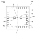
- FIG. 3 is a bottom view of the circuit module of FIG. 1 viewed from the direction of arrow III.
- FIG. 4 is a plan view showing a circuit configuration of the circuit module according to Embodiment 1 of the present invention.
- FIG. 5 is a cross-sectional view of the circuit module of FIG. 4 as viewed from the direction of arrows VV.
- the circuit module 100 includes a laminated substrate 110, a heat generating electronic component 120, a thermal via 175, a ground terminal 172, an external connection terminal 171, and the like. And a fixing contact 173.
- the circuit module 100 according to the present embodiment is a high-frequency module used for a wireless LAN (Local Area Network), but the configuration of the circuit module is not limited to the high-frequency module.
- the laminated substrate 110 has a first main surface 111 and a second main surface 112 located on the opposite side of the first main surface 111 in the stacking direction.
- the multilayer substrate 110 has a rectangular outer shape when viewed from a direction orthogonal to the first main surface 111.
- the outer shape viewed from the direction orthogonal to the first main surface 111 of the multilayer substrate 110 is not limited to a rectangular shape, and may be a circular shape or an elliptical shape.
- the heat-generating electronic component 120 is mounted such that the center C2 is located at a position shifted from the center C on the first main surface 111 when viewed from the direction perpendicular to the first main surface 111.
- the heat-generating electronic component 120 is mounted on the first main surface 111 at a position biased to the right.
- the heat-generating electronic component 120 is a transceiver IC having high-frequency input / output terminals RF1 and RF2.
- the heat generating electronic component 120 may be a SoC (System on Chip) in which a transceiver IC and a baseband IC are integrated.
- the high frequency input / output terminal RF1 corresponds to a frequency in the 2.4 GHz band.
- the high frequency input / output terminal RF2 corresponds to a frequency of 5 GHz band.
- the high frequency input / output terminals RF ⁇ b> 1 and RF ⁇ b> 2 are provided on the left side portion of the heat generating electronic component 120.
- a high frequency circuit 130 is provided on the first main surface 111 of the multilayer substrate 110.
- the high-frequency circuit 130 is disposed on the first main surface 111 at a position biased to the left side.
- the high frequency circuit 130 includes filters 131 and 132, a switch circuit 133, and a matching circuit 134.
- the filter 131 is connected to the high-frequency input / output terminal RF1, passes a signal wave having a frequency of 2.4 GHz band, and blocks harmonics of the signal wave.
- the filter 132 is connected to the high-frequency input / output terminal RF2, passes a signal wave having a frequency of 5 GHz, and blocks harmonics of the signal wave.
- the switch circuit 133 selectively connects either the filter 131 or the filter 132 and the matching circuit 134.
- the matching circuit 134 matches the impedance between the transmission path in the circuit module 100 and the antenna.
- a power supply circuit 140 and a reference oscillation circuit 150 are provided on the first main surface 111 of the multilayer substrate 110.
- the power supply circuit 140 and the reference oscillation circuit 150 are mounted on the first main surface 111 on the front side of the heat-generating electronic component 120.
- the power supply circuit 140 generates a voltage suitable for the heat generating electronic component 120.
- the reference oscillation circuit 150 generates a reference clock when the heat generating electronic component 120 is operated.
- the shield case 160 is fixed on the first main surface 111 of the multilayer substrate 110.
- the heat-generating electronic component 120, the high-frequency circuit 130, the power supply circuit 140, and the reference oscillation circuit 150 are disposed in a space surrounded by the first main surface 111 and the shield case 160.
- the shield case 160 functions as an electromagnetic shield.
- the laminated substrate 110 is configured by laminating a plurality of dielectric layers.
- the multilayer substrate 110 is provided with a plurality of through holes 174 and thermal vias 175 that penetrate the multilayer substrate 110.
- the inner peripheral surface of each of the plurality of through holes 174 and the thermal vias 175 is made of a metal plating film having good electrical and thermal conductivity such as copper.
- the thermal via 175 is located immediately below the heat generating electronic component 120 and is connected to the heat generating electronic component 120 through the solder bump 181.
- the through hole 174 located immediately below the heat generating electronic component 120 is connected to the heat generating electronic component 120 through the solder bump 181.
- a conductor pattern 176 is provided between the layers of the multilayer substrate 110.
- the conductor pattern 176 is connected to the plurality of through holes 174.
- a conductor pattern 177 is provided on the first main surface 111 of the multilayer substrate 110.
- the conductor pattern 177 is connected to each of the plurality of through holes 174 and the thermal vias 175.
- a part of the conductor pattern 177 located immediately below the matching circuit 134 is connected to the matching circuit 134 through the solder bump 181.
- a resist 190 is provided on the first main surface 111 of the multilayer substrate 110 in a portion where the conductor pattern 177 is not provided.
- a plurality of external connection terminals 171 are provided on the peripheral edge on the second main surface 112 of the multilayer substrate 110.
- Each of the plurality of external connection terminals 171 is connected to the corresponding through hole 174 and is electrically connected to the heat-generating electronic component 120.
- each of the plurality of external connection terminals 171 is electrically connected to the heat-generating electronic component 120 through a corresponding transmission path among the through hole 174, the conductor pattern 176, the conductor pattern 177, and the high-frequency circuit 130. ing.
- a ground terminal 172 connected to the thermal via 175 is provided inside the peripheral edge on the second main surface 112.
- the ground terminal 172 is arranged at a position shifted from the center on the second main surface 112.
- the ground terminal 172 is disposed at a position overlapping the central portion of the heat-generating electronic component 120 when viewed from the direction orthogonal to the second main surface 112.
- a first imaginary straight line connecting the center C of the second major surface 112 and the center of the ground terminal 172 is L1, and the first imaginary straight line L1.
- a second imaginary straight line that is orthogonal to each other and passes through the center C of the second major surface 112 is denoted by L2.
- the fixing contact 173 is provided in the second region T2 adjacent to the first region T1 on the side where the ground terminal 172 is located, with the second virtual straight line L2 as a boundary, inside the peripheral edge on the second main surface 112. It has been.
- the ground terminal 172 is located on the right side and the fixing contact 173 is located on the left side as viewed from the second virtual straight line L2.
- the fixing contact 173 is disposed at a position symmetrical to the ground terminal 172 with respect to the second virtual straight line L2.
- one fixing contact 173 is provided, but a plurality of fixing contacts 173 may be provided as long as at least one is provided.
- the fixing contact 173 is not connected to the through hole 174 and the thermal via 175.
- FIG. 6 is a cross-sectional view showing a state in which the circuit module according to the comparative example is mounted on the device board.
- the fixing contact 173 is not provided, and each of the plurality of external connection terminals 171 and ground terminals 172 and the terminal of the device substrate 910 are joined to each other. ing. Since the ground terminal 172 is biased and positioned inside the peripheral edge of the second main surface 112 of the multilayer substrate 110, the external connection terminal located farthest from the ground terminal 172 on the second main surface 112 of the multilayer substrate 110. A region between 171 and the ground terminal 172 is a non-joined region N that is not joined to the terminal of the device substrate 910.
- the multilayer substrate 110 When the multilayer substrate 110 expands due to heat generated by the heat-generating electronic component 120, the multilayer substrate 110 protrudes in a convex shape in a direction away from the device substrate 910 in the non-joint region N, and the second main of the device substrate 910 and the multilayer substrate 110.
- the gap H with the surface 112 is increased.
- the stress S in the direction away from the device substrate 910 may act on the external connection terminal 171 located farthest from the ground terminal 172, which may cause poor bonding.
- each of the plurality of external connection terminals 171, the ground terminals 172, the fixing contacts 173 and the terminals of the device substrate 910 are joined to each other, whereby the non-joining region N is formed.
- the laminated substrate 110 expands due to heat generated by the heat-generating electronic component 120, the floating of the laminated substrate 110 can be suppressed.
- the stress S in the direction away from the device substrate 910 is distributed and applied to the external connection terminal 171 and the fixing contact 173, it is possible to suppress the occurrence of poor bonding between the circuit module 100 and the device substrate 910, and the circuit module.
- the durability against thermal expansion and contraction of 100 can be increased.
- circuit module according to Embodiment 2 of the present invention is mainly different from the circuit module 100 according to the first embodiment in that it corresponds to MIMO (multiple-input and multiple-output). The description of the same configuration as that of module 100 will not be repeated.
- MIMO multiple-input and multiple-output
- FIG. 7 is a plan view showing a circuit configuration of a circuit module according to Embodiment 2 of the present invention.
- FIG. 8 is a bottom view showing the appearance of the circuit module according to the second embodiment of the present invention.
- FIG. 7 shows a state where the shield case is removed. In FIG. 8, the resist is not shown for easy viewing.
- the circuit module 200 includes a laminated substrate 110, a heat generating electronic component 120, a ground terminal 172 connected to the thermal via 175, and an external connection terminal. 171 and a fixing contact 273.
- the heat-generating electronic component 120 is a transceiver IC having high-frequency input / output terminals RF1, RF2, RF3, and RF4.
- the high frequency input / output terminals RF1 and RF3 correspond to frequencies in the 2.4 GHz band.
- the high frequency input / output terminals RF2 and RF4 correspond to a frequency of 5 GHz band.
- the high frequency input / output terminals RF 1, RF 2, RF 3, and RF 4 are provided on the left side of the heat-generating electronic component 120.
- a high frequency circuit 230 is provided on the first main surface 111 of the multilayer substrate 110.
- the high frequency circuit 230 is disposed on the first main surface 111 at a position biased to the left side.
- High-frequency circuit 230 includes a first system composed of filters 131 and 132, switch circuit 133 and matching circuit 134, and a second system composed of filters 231 and 232, switch circuit 233 and matching circuit 234.
- the filter 231 is connected to the high-frequency input / output terminal RF3, passes a signal wave having a frequency of 2.4 GHz band, and blocks harmonics of the signal wave.
- the filter 232 is connected to the high-frequency input / output terminal RF4, passes a signal wave having a frequency of 5 GHz band, and blocks harmonics of the signal wave.
- the switch circuit 233 selectively connects either the filter 231 or the filter 232 and the matching circuit 234.
- the matching circuit 234 matches the impedance between the transmission line in the circuit module 200 and the antenna.
- each of the four fixing contacts 273 is not connected to the through hole 174 and the thermal via 175.
- the four fixing contacts 273 are provided on the opposite side to the side where the ground terminal 172 is located, with the second virtual straight line L2 as a boundary, inside the peripheral edge on the second main surface 112.
- the ground terminal 172 when viewed from the second virtual straight line L2, the ground terminal 172 is located on the right side, and the four fixing contacts 273 are located on the left side.
- the four fixing contacts 273 are arranged in parallel with the second virtual straight line L2.
- each of the four fixing contacts 273 is provided at a position overlapping the corresponding high-frequency input / output terminals RF1, RF2, RF3, and RF4.
- the fixing contact 273 that overlaps the high-frequency input / output terminal RF1 is arranged at a position symmetrical to the fixing contact 273 that overlaps the high-frequency input / output terminal RF4 with respect to the first virtual straight line L1.
- the fixing contact 273 that overlaps the high-frequency input / output terminal RF2 is arranged in a line-symmetrical position with the fixing contact 273 that overlaps the high-frequency input / output terminal RF3 with respect to the first virtual straight line L1.
- a part of each of the four fixing contacts 273 overlaps the heat-generating electronic component 120 when viewed from the direction perpendicular to the second main surface 112.
- each of the four fixing contacts 273 is located closer to the center C of the second main surface 112 than the ground terminal 172.
- the distance between the ground terminal 172 and the center C is D1
- the distance between the fixing contact 273 that overlaps the high frequency input / output terminal RF1 and the center C is D3, which overlaps the high frequency input / output terminal RF2.
- the distance between the fixing contact 273 and the center C is D2
- the distance between the fixing contact 273 and the center C overlapping the high frequency input / output terminal RF3 is D2
- circuit module 200 Since the circuit module 200 according to the present embodiment is compatible with MIMO, both the wireless communication circuits of the first system and the second system operate simultaneously, and heat is generated as compared with the circuit module 100 according to the first embodiment.
- the calorific value of the conductive electronic component 120 is large.
- the four fixing contacts 273 are arranged at positions overlapping the corresponding high-frequency input / output terminals RF1, RF2, RF3, and RF4 when viewed from the direction perpendicular to the second main surface 112, so that the heat generating electrons A heat dissipation path from the component 120 through the multilayer substrate 110 can be secured.
- the temperature increase of the wireless communication circuit can be reduced and deterioration of various characteristics of the wireless communication can be suppressed.
- the fixing contact 273 is located closer to the center C of the second main surface 112 than the ground terminal 172 on the second main surface 112, it is difficult to reduce the non-bonded region N.
- the plurality of fixing contacts 273 are provided, the stress in the direction away from the device board is distributed and applied to the external connection terminals 171 and the fixing contacts 273, so that the circuit module 200 and the device board The occurrence of poor bonding can be suppressed, and the durability of the circuit module 200 against thermal expansion and contraction can be enhanced.
- the four fixing contacts 273 are arranged in parallel with the second imaginary straight line L2, it is possible to suppress the multilayer substrate 110 from being twisted due to heat generated by the heat-generating electronic component 120.
- Each of the four fixing contacts 273 may be connected to the ground electrode of the device board. In this case, each of the four fixing contacts 273 can be stably grounded. As a result, the reference potential of the transmission line in the vicinity of the high frequency input / output terminals RF1, RF2, RF3, and RF4 where impedance discontinuity is likely to occur can be stabilized, and the characteristic impedance of the transmission line in the circuit module 200 can be stabilized. . Moreover, the common impedance which the transmission line in the multilayer substrate 110 has can be reduced. As a result, deterioration of the high frequency characteristics of the circuit module 200 can be suppressed.
Abstract
Selon la présente invention, un substrat stratifié (110) comporte une première surface principale (111) et une seconde surface principale (112) qui se trouve sur le côté opposé à la première surface principale (111) dans la direction de stratification. Lorsqu'il est observé depuis la direction perpendiculaire à la première surface principale (111), un composant électronique producteur de chaleur (120) est monté de telle sorte qu'un centre (C2) est positionné à une position décalée d'un centre (C) sur la première surface principale (111). Une borne de mise à la terre (172) est disposée sur la seconde surface principale (112). La borne de mise à la terre (172) est connectée à un trou d'interconnexion thermique (175). Sur le côté interne d'une section d'extrémité périphérique sur la seconde surface principale (112), un point de contact de fixation (173) est disposé dans une seconde région (T2) qui est adjacente à une première région (T1) en ayant, en tant que limite, une seconde ligne droite virtuelle, qui est orthogonale à une première ligne droite virtuelle connectant la borne de mise à la terre (172) et le centre (C) de la seconde surface principale (112) l'un par rapport à l'autre, et qui passe au centre (C) de la seconde surface principale (112), ladite première région se trouvant sur le côté où la borne de mise à la terre (172) est positionnée.
Applications Claiming Priority (2)
| Application Number | Priority Date | Filing Date | Title |
|---|---|---|---|
| JP2017094785 | 2017-05-11 | ||
| JP2017-094785 | 2017-05-11 |
Publications (1)
| Publication Number | Publication Date |
|---|---|
| WO2018207600A1 true WO2018207600A1 (fr) | 2018-11-15 |
Family
ID=64105100
Family Applications (1)
| Application Number | Title | Priority Date | Filing Date |
|---|---|---|---|
| PCT/JP2018/016409 WO2018207600A1 (fr) | 2017-05-11 | 2018-04-23 | Module de circuit |
Country Status (1)
| Country | Link |
|---|---|
| WO (1) | WO2018207600A1 (fr) |
Cited By (1)
| Publication number | Priority date | Publication date | Assignee | Title |
|---|---|---|---|---|
| TWI742517B (zh) * | 2019-01-30 | 2021-10-11 | 聯發科技股份有限公司 | 半導體封裝和印刷電路板 |
Citations (4)
| Publication number | Priority date | Publication date | Assignee | Title |
|---|---|---|---|---|
| JP2003008469A (ja) * | 2001-06-21 | 2003-01-10 | Kyocera Corp | 高周波モジュール |
| JP2005277075A (ja) * | 2004-03-24 | 2005-10-06 | Kyocera Corp | 配線基板 |
| JP2006269976A (ja) * | 2005-03-25 | 2006-10-05 | Renesas Technology Corp | 電子装置の製造方法および多層配線基板の製造方法 |
| JP2013084749A (ja) * | 2011-10-07 | 2013-05-09 | Murata Mfg Co Ltd | 電子部品 |
-
2018
- 2018-04-23 WO PCT/JP2018/016409 patent/WO2018207600A1/fr active Application Filing
Patent Citations (4)
| Publication number | Priority date | Publication date | Assignee | Title |
|---|---|---|---|---|
| JP2003008469A (ja) * | 2001-06-21 | 2003-01-10 | Kyocera Corp | 高周波モジュール |
| JP2005277075A (ja) * | 2004-03-24 | 2005-10-06 | Kyocera Corp | 配線基板 |
| JP2006269976A (ja) * | 2005-03-25 | 2006-10-05 | Renesas Technology Corp | 電子装置の製造方法および多層配線基板の製造方法 |
| JP2013084749A (ja) * | 2011-10-07 | 2013-05-09 | Murata Mfg Co Ltd | 電子部品 |
Cited By (1)
| Publication number | Priority date | Publication date | Assignee | Title |
|---|---|---|---|---|
| TWI742517B (zh) * | 2019-01-30 | 2021-10-11 | 聯發科技股份有限公司 | 半導體封裝和印刷電路板 |
Similar Documents
| Publication | Publication Date | Title |
|---|---|---|
| JP6750738B2 (ja) | アンテナモジュールおよび通信装置 | |
| JP6821008B2 (ja) | マイクロ波デバイス及び空中線 | |
| TWI493893B (zh) | 高頻電路模組 | |
| JP5931851B2 (ja) | ノイズ抑制構造を有する回路基板 | |
| JPWO2006035518A1 (ja) | Rf回路モジュール | |
| KR102153867B1 (ko) | 안테나 모듈, 및 안테나 모듈의 제조 방법 | |
| KR101385167B1 (ko) | 프린트 회로판 | |
| US20210005578A1 (en) | Radio-frequency module and communication apparatus | |
| US9705194B2 (en) | Antenna module | |
| US8558641B2 (en) | High-frequency module | |
| JP2014042094A (ja) | 高周波回路モジュール | |
| CN110896165B (zh) | 片上天线 | |
| JP5422078B1 (ja) | 高周波回路モジュール | |
| TW201503482A (zh) | 電子電路及電子機器 | |
| JPWO2013047358A1 (ja) | 高周波モジュール | |
| JP2017187379A (ja) | 多層基板回路モジュール、無線通信装置およびレーダ装置 | |
| JP5472551B2 (ja) | 高周波信号線路及び電子機器 | |
| GB2571214A (en) | Terminal device | |
| JP5686630B2 (ja) | プリント配線板、光通信モジュール、光通信装置、モジュール装置および演算処理装置 | |
| WO2018207600A1 (fr) | Module de circuit | |
| WO2020217321A1 (fr) | Dispositif électrique | |
| JP2001320170A (ja) | 多層基板モジュール | |
| JP2014099839A (ja) | 高周波回路モジュール | |
| WO2021006037A1 (fr) | Ligne de transmission et instrument électronique | |
| US20210410269A1 (en) | High-frequency circuit and communication module |
Legal Events
| Date | Code | Title | Description |
|---|---|---|---|
| 121 | Ep: the epo has been informed by wipo that ep was designated in this application |
Ref document number: 18798022 Country of ref document: EP Kind code of ref document: A1 |
|
| NENP | Non-entry into the national phase |
Ref country code: DE |
|
| 122 | Ep: pct application non-entry in european phase |
Ref document number: 18798022 Country of ref document: EP Kind code of ref document: A1 |
|
| NENP | Non-entry into the national phase |
Ref country code: JP |