WO2018207575A1 - 接着剤層形成装置、半導体チップ製造ライン、及び積層体の製造方法 - Google Patents
接着剤層形成装置、半導体チップ製造ライン、及び積層体の製造方法 Download PDFInfo
- Publication number
- WO2018207575A1 WO2018207575A1 PCT/JP2018/016038 JP2018016038W WO2018207575A1 WO 2018207575 A1 WO2018207575 A1 WO 2018207575A1 JP 2018016038 W JP2018016038 W JP 2018016038W WO 2018207575 A1 WO2018207575 A1 WO 2018207575A1
- Authority
- WO
- WIPO (PCT)
- Prior art keywords
- adhesive layer
- semiconductor wafer
- closed space
- layer forming
- forming apparatus
- Prior art date
Links
Images


Classifications
-
- H—ELECTRICITY
- H01—ELECTRIC ELEMENTS
- H01L—SEMICONDUCTOR DEVICES NOT COVERED BY CLASS H10
- H01L21/00—Processes or apparatus adapted for the manufacture or treatment of semiconductor or solid state devices or of parts thereof
- H01L21/67—Apparatus specially adapted for handling semiconductor or electric solid state devices during manufacture or treatment thereof; Apparatus specially adapted for handling wafers during manufacture or treatment of semiconductor or electric solid state devices or components ; Apparatus not specifically provided for elsewhere
- H01L21/67005—Apparatus not specifically provided for elsewhere
- H01L21/67011—Apparatus for manufacture or treatment
- H01L21/67132—Apparatus for placing on an insulating substrate, e.g. tape
-
- H—ELECTRICITY
- H01—ELECTRIC ELEMENTS
- H01L—SEMICONDUCTOR DEVICES NOT COVERED BY CLASS H10
- H01L21/00—Processes or apparatus adapted for the manufacture or treatment of semiconductor or solid state devices or of parts thereof
- H01L21/67—Apparatus specially adapted for handling semiconductor or electric solid state devices during manufacture or treatment thereof; Apparatus specially adapted for handling wafers during manufacture or treatment of semiconductor or electric solid state devices or components ; Apparatus not specifically provided for elsewhere
- H01L21/67005—Apparatus not specifically provided for elsewhere
- H01L21/67011—Apparatus for manufacture or treatment
- H01L21/67155—Apparatus for manufacturing or treating in a plurality of work-stations
- H01L21/6719—Apparatus for manufacturing or treating in a plurality of work-stations characterized by the construction of the processing chambers, e.g. modular processing chambers
-
- H—ELECTRICITY
- H01—ELECTRIC ELEMENTS
- H01L—SEMICONDUCTOR DEVICES NOT COVERED BY CLASS H10
- H01L21/00—Processes or apparatus adapted for the manufacture or treatment of semiconductor or solid state devices or of parts thereof
- H01L21/70—Manufacture or treatment of devices consisting of a plurality of solid state components formed in or on a common substrate or of parts thereof; Manufacture of integrated circuit devices or of parts thereof
- H01L21/71—Manufacture of specific parts of devices defined in group H01L21/70
- H01L21/768—Applying interconnections to be used for carrying current between separate components within a device comprising conductors and dielectrics
- H01L21/76838—Applying interconnections to be used for carrying current between separate components within a device comprising conductors and dielectrics characterised by the formation and the after-treatment of the conductors
- H01L21/76841—Barrier, adhesion or liner layers
-
- B—PERFORMING OPERATIONS; TRANSPORTING
- B05—SPRAYING OR ATOMISING IN GENERAL; APPLYING FLUENT MATERIALS TO SURFACES, IN GENERAL
- B05D—PROCESSES FOR APPLYING FLUENT MATERIALS TO SURFACES, IN GENERAL
- B05D3/00—Pretreatment of surfaces to which liquids or other fluent materials are to be applied; After-treatment of applied coatings, e.g. intermediate treating of an applied coating preparatory to subsequent applications of liquids or other fluent materials
- B05D3/12—Pretreatment of surfaces to which liquids or other fluent materials are to be applied; After-treatment of applied coatings, e.g. intermediate treating of an applied coating preparatory to subsequent applications of liquids or other fluent materials by mechanical means
-
- B—PERFORMING OPERATIONS; TRANSPORTING
- B32—LAYERED PRODUCTS
- B32B—LAYERED PRODUCTS, i.e. PRODUCTS BUILT-UP OF STRATA OF FLAT OR NON-FLAT, e.g. CELLULAR OR HONEYCOMB, FORM
- B32B37/00—Methods or apparatus for laminating, e.g. by curing or by ultrasonic bonding
-
- B—PERFORMING OPERATIONS; TRANSPORTING
- B32—LAYERED PRODUCTS
- B32B—LAYERED PRODUCTS, i.e. PRODUCTS BUILT-UP OF STRATA OF FLAT OR NON-FLAT, e.g. CELLULAR OR HONEYCOMB, FORM
- B32B37/00—Methods or apparatus for laminating, e.g. by curing or by ultrasonic bonding
- B32B37/12—Methods or apparatus for laminating, e.g. by curing or by ultrasonic bonding characterised by using adhesives
- B32B37/1284—Application of adhesive
-
- B—PERFORMING OPERATIONS; TRANSPORTING
- B32—LAYERED PRODUCTS
- B32B—LAYERED PRODUCTS, i.e. PRODUCTS BUILT-UP OF STRATA OF FLAT OR NON-FLAT, e.g. CELLULAR OR HONEYCOMB, FORM
- B32B7/00—Layered products characterised by the relation between layers; Layered products characterised by the relative orientation of features between layers, or by the relative values of a measurable parameter between layers, i.e. products comprising layers having different physical, chemical or physicochemical properties; Layered products characterised by the interconnection of layers
- B32B7/04—Interconnection of layers
- B32B7/12—Interconnection of layers using interposed adhesives or interposed materials with bonding properties
-
- B—PERFORMING OPERATIONS; TRANSPORTING
- B32—LAYERED PRODUCTS
- B32B—LAYERED PRODUCTS, i.e. PRODUCTS BUILT-UP OF STRATA OF FLAT OR NON-FLAT, e.g. CELLULAR OR HONEYCOMB, FORM
- B32B9/00—Layered products comprising a layer of a particular substance not covered by groups B32B11/00 - B32B29/00
- B32B9/005—Layered products comprising a layer of a particular substance not covered by groups B32B11/00 - B32B29/00 comprising one layer of ceramic material, e.g. porcelain, ceramic tile
-
- H—ELECTRICITY
- H01—ELECTRIC ELEMENTS
- H01L—SEMICONDUCTOR DEVICES NOT COVERED BY CLASS H10
- H01L21/00—Processes or apparatus adapted for the manufacture or treatment of semiconductor or solid state devices or of parts thereof
- H01L21/67—Apparatus specially adapted for handling semiconductor or electric solid state devices during manufacture or treatment thereof; Apparatus specially adapted for handling wafers during manufacture or treatment of semiconductor or electric solid state devices or components ; Apparatus not specifically provided for elsewhere
- H01L21/67005—Apparatus not specifically provided for elsewhere
- H01L21/67011—Apparatus for manufacture or treatment
- H01L21/67126—Apparatus for sealing, encapsulating, glassing, decapsulating or the like
-
- H—ELECTRICITY
- H01—ELECTRIC ELEMENTS
- H01L—SEMICONDUCTOR DEVICES NOT COVERED BY CLASS H10
- H01L21/00—Processes or apparatus adapted for the manufacture or treatment of semiconductor or solid state devices or of parts thereof
- H01L21/67—Apparatus specially adapted for handling semiconductor or electric solid state devices during manufacture or treatment thereof; Apparatus specially adapted for handling wafers during manufacture or treatment of semiconductor or electric solid state devices or components ; Apparatus not specifically provided for elsewhere
- H01L21/683—Apparatus specially adapted for handling semiconductor or electric solid state devices during manufacture or treatment thereof; Apparatus specially adapted for handling wafers during manufacture or treatment of semiconductor or electric solid state devices or components ; Apparatus not specifically provided for elsewhere for supporting or gripping
- H01L21/6835—Apparatus specially adapted for handling semiconductor or electric solid state devices during manufacture or treatment thereof; Apparatus specially adapted for handling wafers during manufacture or treatment of semiconductor or electric solid state devices or components ; Apparatus not specifically provided for elsewhere for supporting or gripping using temporarily an auxiliary support
- H01L21/6836—Wafer tapes, e.g. grinding or dicing support tapes
-
- H—ELECTRICITY
- H01—ELECTRIC ELEMENTS
- H01L—SEMICONDUCTOR DEVICES NOT COVERED BY CLASS H10
- H01L24/00—Arrangements for connecting or disconnecting semiconductor or solid-state bodies; Methods or apparatus related thereto
- H01L24/80—Methods for connecting semiconductor or other solid state bodies using means for bonding being attached to, or being formed on, the surface to be connected
-
- B—PERFORMING OPERATIONS; TRANSPORTING
- B32—LAYERED PRODUCTS
- B32B—LAYERED PRODUCTS, i.e. PRODUCTS BUILT-UP OF STRATA OF FLAT OR NON-FLAT, e.g. CELLULAR OR HONEYCOMB, FORM
- B32B38/00—Ancillary operations in connection with laminating processes
- B32B38/16—Drying; Softening; Cleaning
- B32B38/164—Drying
- B32B2038/168—Removing solvent
-
- B—PERFORMING OPERATIONS; TRANSPORTING
- B32—LAYERED PRODUCTS
- B32B—LAYERED PRODUCTS, i.e. PRODUCTS BUILT-UP OF STRATA OF FLAT OR NON-FLAT, e.g. CELLULAR OR HONEYCOMB, FORM
- B32B2457/00—Electrical equipment
- B32B2457/14—Semiconductor wafers
Definitions
- the present invention relates to an adhesive layer forming apparatus, a semiconductor chip manufacturing line, and a method for manufacturing a laminate. More specifically, an apparatus (adhesive layer forming apparatus) for forming an adhesive layer on at least one surface of a semiconductor wafer, a semiconductor chip manufacturing line having the adhesive layer forming apparatus, and at least one of the semiconductor wafers
- the present invention relates to a method for manufacturing a laminate having an adhesive layer on a surface.
- silicon wafers are stacked and bonded with an adhesive.
- WOW method wafer-on-wafer method
- a silicon wafer on which a transistor circuit is formed is laminated in units of wafers via an adhesive without being cut into chips.
- Non-Patent Document 1 When the vacuum dryer is large, there are problems that the time for depressurizing the inside of the vacuum dryer and the time for returning to the normal pressure become long, and it becomes difficult to control the temperature uniformly in the vacuum dryer under reduced pressure. Therefore, as a result, there is a problem that the effect of shortening the tact time by using a commercially available vacuum dryer does not appear remarkably.
- the present inventors have removed the coating film formed by applying the adhesive composition under reduced pressure in a closed space having a specific volume or less, and removing the solvent from the adhesive layer. It has been found that a semiconductor wafer having an adhesive layer in which the adhesive layer is difficult to foam during wafer bonding under reduced pressure can be produced while the adhesive is hardly cured and the tact time is shortened. It was. The present invention has been completed based on these findings.
- the present invention is an apparatus for forming an adhesive layer by removing a solvent in a coating film formed on one surface of a semiconductor wafer, the lower plate on which the semiconductor wafer is placed, and the lower part
- an adhesive layer forming apparatus comprising: an upper cover that forms a closed space with a plate of 10 liters or less; and a decompression unit that decompresses the inside of the closed space.
- a portion of the upper cover that becomes a ceiling of the closed space is a dome shape.
- the dome shape portion of the upper cover is made of metal, and the thickness of the dome shape portion is 2 mm or less.
- the adhesive layer forming apparatus preferably has a heating means for heating the coating film.
- the upper cover has a flange portion on the periphery, and the lower plate contacts the flange portion on the mounting table on which the semiconductor wafer is mounted, and closes the mounting plate. It is preferable to have a groove that forms a space.
- the adhesive layer forming apparatus has a thermocouple at a position where the closed space and the ventilation are blocked inside the lower plate.
- the adhesive layer forming apparatus further includes a vertical drive unit that includes a hook unit and a ball unit, and opens and closes the closed space by moving the upper cover up and down, and the upper cover includes the decompression unit and the closing unit. It is preferable to connect to a branch pipe connected to a decompression means for returning the space to normal pressure.
- a gas inflow guard that prevents the upper cover from being directly blown onto the surface of the adhesive layer on which the gas flowing into the closed space is formed when the closed space is returned to normal pressure. It is preferable to have it inside the part into which flows.
- the hook unit is connected to a jack via an arm.
- the present invention also provides an adhesive composition coating apparatus for forming a coating film by applying an adhesive composition containing an adhesive component and a solvent to one surface of the semiconductor wafer, the adhesive layer forming apparatus, and A semiconductor chip manufacturing line having an apparatus for bonding a semiconductor wafer having an adhesive layer to another semiconductor wafer in this order is provided.
- the present invention is also a method for producing a laminate having an adhesive layer on at least one surface of a semiconductor wafer, wherein an adhesive composition containing an adhesive component and a solvent is applied to one surface of the semiconductor wafer.
- a method for producing a laminate comprising a step of forming a coating film, and a step of forming an adhesive layer by removing the solvent in the coating film under reduced pressure in a closed space having a volume of 10 liters or less.
- the present invention is also a method for producing a laminate having an adhesive layer on at least one surface of a semiconductor wafer, wherein an adhesive composition containing an adhesive component and a solvent is applied to one surface of the semiconductor wafer.
- a method for producing a laminate which includes a step of forming a coating film and a step of forming an adhesive layer by removing the solvent in the coating film using the adhesive layer forming apparatus.
- the adhesive layer forming apparatus of the present invention since it has the above-described configuration, it is a laminate having an adhesive layer on one surface of a semiconductor wafer, and is bonded when the wafer is bonded under reduced pressure.
- a laminate in which the agent layer is difficult to foam can be produced while preventing the adhesive from being hardened and shortening the tact time.
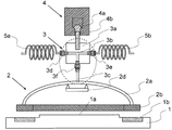
- FIG. 1 It is the schematic (front sectional drawing) which shows an example of the adhesive bond layer forming apparatus of this invention.
- A is a top view of the upper cover 2 comprised by the dome shape part 2a and the flange part 2b, (b) is a cross-sectional front view of the bb 'cross section in (a).
- A) is a top view of the lower plate 1, and (b) is a cross-sectional front view of the b-b ′ cross section in (a).
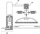
- FIG. 1 It is the schematic which shows an example in which the hook unit 4b and the jack 6a of the vertical drive unit 4 are connected via the arm 6b.
- FIG. 3 is a schematic view showing a mode in which a heating plate 8 is provided on the lower side of the lower plate 1. It is an enlarged view (perspective view) of the gas inflow guard 2d.
- (A) is the schematic (top view) which shows the aspect before and behind conveying a semiconductor wafer from the adhesive composition coating device to the adhesive layer forming apparatus of this invention by a conveyance means
- (b) is a semiconductor by a conveyance means. It is the schematic (top view) which shows the aspect before and behind conveying a wafer from the adhesive bond layer forming apparatus of this invention to a semiconductor wafer lamination apparatus.
- (A) is a top view of a pick-up jig
- (b) is a left side view.
- the adhesive layer forming apparatus of the present invention is an apparatus (adhesive layer forming apparatus) that forms an adhesive layer by removing a solvent (solvent) in a coating film formed on one surface of a semiconductor wafer.
- the adhesive layer forming apparatus of the present invention includes a lower plate on which a semiconductor wafer is placed, an upper cover that forms a closed space with a volume of 10 liters or less with the lower plate, a decompression unit that decompresses the inside of the closed space, Is provided.
- FIG. 1 is a schematic view (front sectional view) showing an example of the adhesive layer forming apparatus of the present invention.
- the adhesive layer forming apparatus of the present invention shown in FIG. 1 has a plate-like lower plate 1 and an upper cover 2. By moving the upper cover 2 downward and bringing it into contact with the lower plate 1, the upper cover 2 and the lower plate 1 can form a closed space with a volume of 10 liters or less. In addition, since the closed space is formed and opened by the vertical movement of the upper cover 2, it is not necessary to install an opening / closing door.
- the volume of the closed space formed by the upper cover 2 and the lower plate 1 is 10 liters or less (for example, 0.1 to 10 liters), preferably 8 liters or less (for example, 0.1 to 10 liters). 8 liters), more preferably 7 liters or less (for example, 0.1 to 7 liters).
- the upper cover 2 has a dome-shaped (saddle-shaped) portion as a ceiling of the closed space, and has a dome-shaped portion 2a and a flange portion 2b that are dome-shaped.
- FIG. 2 shows a top view (a) of the upper cover 2 composed of the dome-shaped portion 2a and the flange portion 2b, and a cross-sectional front view (b) taken along the line b-b 'in the top view (a).
- the upper cover 2 has a dome-shaped portion 2a that is circular at the center when viewed from above, and the center of the circle of the dome-shaped portion 2a is used to suck and depressurize the inside of the closed space.
- a hole 2c is provided, and a flange portion 2b is provided along the circumference on the periphery of the dome-shaped portion 2a.
- the upper cover 2 has a dome shape, but in this specification, the “dome shape” means that the angle of the cross section with respect to the horizontal plane gradually increases from the center (hole 2c) when viewed from above.
- the center of the circle is a gently convex shape, and includes a hemispherical shape and a semi-elliptical spherical shape.
- the closed space Due to the dome shape of the upper cover 2, when the closed space is formed by the upper cover 2 and the lower plate 1, the closed space has a sufficient space for placing a semiconductor wafer having a thickness of less than 1 mm. In addition, it is possible to form a closed space in which the internal volume is minimized.
- the upper cover 2 is not limited to a dome-shaped one, and may have other shapes as long as it can form a closed space having the specific volume or less.
- the dome-shaped portion 2a has different curvatures near the dome-shaped edge (near the flange portion 2b) r1 and near the dome-shaped bottom (near the hole 2c) r2.
- the radius of curvature of the vicinity r2 is larger than the radius of curvature of the vicinity r1 of the edge.
- the height h from the bottom of the dome shape to the edge of the dome shape is preferably 50 to 120 mm from the viewpoint of easy desolvation of the coating film.
- the diameter w1 of the edge surface inside the dome shape is preferably slightly larger than the size of the semiconductor wafer, and is, for example, 100 to 500 mm.
- the difference (diameter of the flange portion 2b) w2 between the diameter of the circle having the inner edge of the flange 2b and the diameter of the circle having the outer edge as a circumference is preferably 5 to 30 mm.
- the thickness t of the flange portion 2b is preferably 3 to 20 mm.
- the thickness of the dome-shaped portion 2a is preferably 5 mm or less, more preferably 2 mm or less from the viewpoint of weight reduction.
- the material constituting the dome-shaped portion 2a of the upper cover 2 includes metal, resin, glass and the like, but from the viewpoint of weight reduction and strength against decompression of the closed space, metal is preferable, and SUS is particularly preferable. That is, the dome-shaped portion 2a is preferably made of metal, particularly preferably SUS.
- the adhesive layer forming apparatus of the present invention prevents the closed space from being depressed due to a difference from the atmospheric pressure under a reduced pressure even if the dome-shaped portion 2a of the upper cover 2 is a thin metal plate processed into a curved surface. Further, by using such a dome-shaped portion 2a, the weight of the upper cover 2 can be reduced, and the power and mechanism required above and below the upper cover 2 can be minimized.
- the lower plate 1 has a square shape when viewed from above, and has a mounting table 1a for mounting a semiconductor wafer on which a coating film is formed. Further, the lower plate 1 has a groove 1b that forms a closed space in contact with the flange portion 2b (particularly, the bottom portion of the flange portion 2b) of the upper cover 2 around the mounting table 1a.
- FIG. 3 shows a top view (a) of the lower plate 1 and a cross-sectional front view (b) taken along the line b-b ′ in the top view (a).
- the mounting table 1a is provided in a circular shape so as to be higher than other portions, and the groove 1b is provided in a ring shape around the mounting table 1a. Since the upper cover 2 has the flange portion 2b and the lower plate 1 has the groove 1b, when the closed space is formed, the upper cover 2 and the lower plate 1 are in contact with each other by the flange portion 2b and the groove 1b. Adhesion between the upper cover 2 and the lower plate 1 is improved, and air is less likely to enter the closed space under reduced pressure.
- the lower plate 1 may not have the groove 1b, and the upper cover 2 may not have the flange portion 2b.
- the adhesive layer forming apparatus of the present invention has a heating means (not shown).
- thermocouple 1c is embedded in the lower plate 1 at a position where the formed closed space and ventilation are blocked. Therefore, the lower plate 1 is provided with a hole for installing the thermocouple 1c. When the thermocouple 1c is used, a temperature closer to the semiconductor wafer can be measured.
- the width w3 and the length w4 of the lower plate 1 are, for example, 200 to 600 mm, depending on the size of the semiconductor wafer on which the coating film is formed.
- the diameter w5 of the mounting table 1a is preferably slightly smaller than the size of the semiconductor wafer from the viewpoint of minimizing the volume of the closed space and facilitating mounting and picking up of the semiconductor wafer, for example, 80 to 470 mm.
- the diameter w6 of the circle having the inner edge of the groove 1b as a circumference is preferably larger than w5 and small as long as it does not contact the semiconductor wafer.
- the difference between the diameter w6 of the circle whose inner edge is the circumference and the diameter of the circle whose outer edge is the circumference (width of the groove 1b) w7 is slightly larger than the width w2 of the flange portion 2b.
- the degree is preferable, for example, 12 to 60 mm.
- the height h2 of the mounting table 1a is preferably 5 to 20 mm.
- the depth h3 of the groove 1b is preferably 1 to 10 mm.
- the material constituting the lower plate 1 examples include metal, resin, glass, and the like. From the viewpoint of strength against reduced pressure in a closed space and thermal conductivity, metal is preferable, and SUS is particularly preferable. That is, the lower plate 1 is preferably made of metal, particularly preferably SUS.
- the bottom of the flange portion 2b and the surface of the groove 1b are subjected to a pair of surface treatments by joint polishing or the like. Accordingly, the flange portion 2b and the groove 1b can be in contact with each other without a gap without using a sealing agent such as vacuum grease, and air does not easily enter the closed space under reduced pressure.
- a sealing agent such as silicone grease
- a packing such as a Teflon sheet
- the upper cover 2 is suspended from the tube branching unit 3.
- a pipe 3c leading to the branch pipe 3b connected to the pressure reducing means and the means for returning to normal pressure (pressure releasing means) is inserted into the hole 2c of the upper cover 2, and a closed space is formed via the pipe 3c.
- the depressurization and decompression are performed.
- the pipe 3c and the upper cover 2 are welded so that air does not enter the closed space when the pressure is reduced.
- the hole 2 c does not need to be provided at the center of the dome shape of the upper cover 2, and may be provided at any location of the upper cover 2.
- a dome-shaped central portion is preferable from the viewpoint of reducing pressure and releasing pressure through the inside of the tube branching unit 3 that suspends the upper cover 2 while hanging.
- the tube branch unit 3 has a branch pipe 3b inside the unit body 3a.
- the unit body 3a has three female screw portions, and tube joints 3d, 3e, and 3f (for example, one-touch joints) having male screw portions are screwed into the female screw portions, and the three ends of the branch pipe 3b are connected. Are connected to the tube joints 3d, 3e and 3f, respectively.
- a pipe 3c is connected to one end of the branch pipe 3b through a tube joint 3f, and the pipe 3c is inserted into the hole 2c of the upper cover 2.
- the other end of the branch pipe 3b is connected to a spiral tube 5a connected to a decompression means (not shown) via a tube joint 3d, and the other end is not shown via a tube joint 3e.
- the decompression means may be connected to the atmosphere via an air filter for preventing dust intrusion, for example.
- the tube branching unit 3 is moved up and down by a vertical driving unit 4 having a ball unit 4a and a hook unit 4b. More specifically, the tip of the rod portion of the ball unit 4a is a male screw portion, and the male screw portion is screwed and fixed to the female screw portion of the unit main body 3a of the tube branching unit 3.
- the tube branch unit 3 and the upper cover 2 are lifted by the ball portion of the ball unit 4a being caught by the hook (state shown in FIG. 1).
- the hook unit 4b is lowered, the tube branching unit 3 and the upper cover 2 are lowered and hooked on the hook until the upper cover 2 comes into contact with the lower plate 1 and the upper cover 2 does not lower.
- the ball portion is separated from the hook, the flange portion 2b of the upper cover 2 is fitted into the groove 1b of the lower plate 1 only by its own weight, and the lower plate 1 and the upper cover 2 form a closed space. Therefore, by moving the vertical drive unit 4 up and down, the upper cover 2 can be moved up and down, thereby opening and closing the closed space.
- the upper cover 2 may be lifted as shown in FIG. 1, but the flange portion 2 b is usually in the groove 1 b of the lower plate 1. It is in a state of being fitted.
- the hook unit 4b of the vertical drive unit 4 is connected to the arm connected to the jack, and when the arm is moved up and down by the jack, the hook unit 4b moves up and down, and the vertical drive unit 4 drives up and down.
- the hook unit 4b of the vertical drive unit 4 and the jack 6a are connected via an arm 6b.
- the vertical drive unit 4 is raised, and when the arm 6b is lowered by the jack 6a, the vertical drive unit 4 is lowered.
- the vertical drive unit 4 is not particularly limited as long as it can be driven up and down, and may be driven up and down by means other than a jack.
- FIG. 5 is a front view of the state in which the vertical drive unit 4 is connected to the arm 6b, a cross-sectional side view of the bb ′ cross section in FIG. 5 (a), and a cross-sectional view of the cc ′ cross section in FIG.
- a cross-sectional top view (c) is shown.
- a recess 4c having a curved bottom is formed near the center of the hook unit 4b, and the ball unit 4a is fixed in the recess 4c without being fixed to the hook unit 4b.
- the depression 4c has a guard at the front so that the ball does not fall to the front surface, and the ball unit 4a is thinner than the diameter of the ball so that the ball unit 4a can be easily detached from the hook unit 4b.
- a column-shaped gap thicker than the cross-sectional diameter is provided at the front. Since the vertical drive unit 4 has such a structure, when the upper cover 2 moves up and down, the upper cover 2 can move relatively freely with the ball portion of the ball unit 4a as a fulcrum. After the upper cover 2 is lowered and comes into contact with the lower plate 1, the ball unit 4a is separated from the hook unit 4b, and the flange portion 2b of the upper cover 2 is fitted into the groove 1b of the lower plate 1 only by its own weight and closed. A space is formed.
- the closed space is opened by simply pulling up the ball unit 4a by the hook unit 4b, and the semiconductor wafer on which the adhesive layer is formed can be taken out. it can.
- an arm 6b is fixed to the rear portion of the hook unit 4b with a mounting screw 6c.
- FIG. 6A shows a state in which the tube branch unit 3 and the upper cover 2 are lifted by the vertical drive unit 4 and a closed space is not formed (the same as the state shown in FIG. 1).
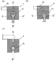
- the semiconductor wafer 7b having the coating film 7a formed by applying the adhesive composition is placed on the mounting table 1a of the lower plate 1 (FIG. 6B).
- the area of the mounting surface of the mounting table 1a is slightly smaller than the area of the bottom surface of the semiconductor wafer 7b.
- the hook unit 4b is lowered until the flange portion 2b of the upper cover 2 comes into contact with the groove 1b of the lower plate 1 and then the ball portion of the ball unit 4a is separated from the hook of the hook unit 4b, thereby forming a closed space.
- the semiconductor wafer 7b in which the coating film 7a is formed is mounted on the mounting table 1a. Then, through the pipe 3c, the branch pipe 3b, and the spiral tube 5a, the inside of the closed space is depressurized from the hole 2c by a decompression unit (not shown) so as to have a specific pressure.
- the pressure in the closed space after depressurization is not particularly limited, but is preferably 0 to 300 mmHg, more preferably 0 to 50 mHg, and still more preferably 0 to 10 mmHg.
- the pressure is 300 mmHg or less (preferably 150 mmHg, particularly 100 mmHg or less)
- the coating film contains a solvent having a high boiling point (for example, a boiling point exceeding 100 ° C. under atmospheric pressure conditions)
- the solvent removal proceeds efficiently in a state where the curing of the agent is less likely to occur.
- the coating film 7a is heated by a heating means (not shown), the solvent in the coating film 7a is volatilized and desolvated, and the adhesive layer 7c is formed (FIG. 6 (d)).
- a heating means not shown
- the inside of the closed space is returned to normal pressure from the hole 2c by a pressure releasing means (not shown) through the pipe 3c, the branch pipe 3b, and the spiral tube 5b.
- the hook unit 4a is lifted, the upper cover 2 is raised, and the semiconductor wafer 7b on which the adhesive layer 7c is formed is brought into a movable state (FIG.
- the gas inflow guard 2d for preventing the gas flowing into the closed space from being directly blown from the hole 2c onto the surface of the adhesive layer is provided inside the portion where the gas flows. That is, it is provided by welding on the inside of the dome-shaped portion 2a of the portion where the hole 2c of the upper cover 2 is provided.
- the temperature of the coating film during the solvent removal is not particularly limited, but is preferably 80 ° C. or lower (eg, 10 to 80 ° C.), more preferably 60 ° C. or lower.
- 80 ° C. or lower it is possible to efficiently remove the solvent while making it harder to cure the adhesive.
- the temperature is 10 ° C. or higher, desolvation efficiently proceeds even when a high boiling point solvent is contained in the coating film (in the adhesive composition).
- it can heat by the said heating means suitably and can make the temperature of a coating film into the said range.
- the heating means is not particularly limited as long as it can heat the coating film.
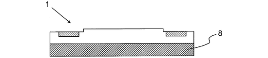
- the heating plate 8 is provided below the lower plate 1 as shown in FIG. 7 (that is, the heating plate 8 is a heating means).
- a mode in which heating means is embedded in the lower plate 1 that is, a mode in which the lower plate 1 is also a heating means).
- the heating means may be integrated with the lower plate 1 or may be separated from the lower plate 1.
- FIG. 8 shows an enlarged view (perspective view) of the gas inflow guard 2d.
- the gas inflow guard 2d has a shape in which four corners of a square are bent into a triangle, and the tips of the triangles at the four corners are welded to the inside of the dome-shaped portion 2a.
- the shape of the gas inflow guard 2d is not particularly limited, and may be any of a circle, an ellipse, and a polygon. Further, the shape of the corner to be bent is not limited to a triangle.
- the gas flows along the inner wall surface of the upper cover 2 to flow into the closed space and can be prevented from being directly sprayed on the surface of the formed adhesive layer.
- the height of the slit-shaped gap (height from the bottom surface of the gas inflow guard 2d to the inner wall of the upper cover 2) is, for example, about 0.5 to 3 mm, preferably about 0.7 to 1.5 mm.
- the adhesive layer forming apparatus of the present invention is not limited to such an apparatus.
- the adhesive layer forming apparatus shown in FIGS. 1 to 8 is preferable.
- the shape of the upper cover as viewed from above is A polygonal upper cover may be used, and a lower plate having a mounting table or a groove having a shape corresponding to the shape of the upper cover may be used as the lower plate.
- the adhesive layer forming apparatus of the present invention is configured to have an upper cover and a lower plate that can form a closed space of a specific volume or less, so there is no need to provide an open / close door, setting of a semiconductor wafer, formation of a closed space, Depressurization in the closed space, desolvation of the coating film, decompression in the closed space, and removal of the semiconductor wafer from the closed space can be easily performed, and the tact time can be shortened. Further, according to the adhesive layer forming apparatus of the present invention, for example, when an adhesive composition using a polyethylene glycol monomethyl ether acetate having a boiling point of 146 ° C. as a solvent is used, the coating film can be removed at 60 ° C. or lower under reduced pressure.
- the solvent can be used, it is difficult for the adhesive component to start the polymerization reaction during the solvent removal, the tact time can be shortened, and the amount of the residual solvent in the adhesive layer can be reduced. Moreover, since the adhesive layer forming apparatus of the present invention has a simple structure, it can be easily incorporated into a semiconductor chip production line.
- semiconductor chip production line By incorporating the adhesive layer forming apparatus of the present invention into a semiconductor chip production line, the semiconductor chip production line of the present invention can be obtained.
- the semiconductor chip production line having the adhesive layer forming apparatus of the present invention may be referred to as “semiconductor chip production line of the present invention”.
- the semiconductor chip production line of the present invention is an apparatus for forming a coating film by applying an adhesive composition containing an adhesive component and a solvent to one surface of a semiconductor wafer before the adhesive layer forming apparatus of the present invention. It is preferable to have an agent composition coating apparatus.
- the semiconductor chip manufacturing line of the present invention has a device (semiconductor wafer stacking device) for bonding a semiconductor wafer having the formed adhesive layer to another semiconductor wafer or the like after the adhesive layer forming device of the present invention. It is preferable. That is, the semiconductor chip production line of the present invention preferably has an adhesive composition coating device, an adhesive layer forming device of the present invention, and a semiconductor wafer laminating device in this order.
- the above-mentioned adhesive composition coating apparatus is an apparatus that forms a coating film by applying an adhesive composition containing an adhesive component and a solvent to one surface of a semiconductor wafer.
- an adhesive composition coating apparatus a known or conventional apparatus having a coater can be used, and among these, a spin coater is preferable.
- the semiconductor wafer After the semiconductor wafer is coated with the adhesive composition on the surface by the adhesive composition coating apparatus to form a coating film, the semiconductor wafer is transported to the adhesive layer forming apparatus of the present invention by the transport means, and the adhesive of the present invention The coating film is removed by the layer forming apparatus to form an adhesive layer. The semiconductor wafer on which the adhesive layer is formed is then transported to the semiconductor wafer laminating apparatus by the transport means.
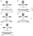
- FIG. 9 is a schematic view (top view) of an example in which a conveying means is incorporated in the semiconductor chip manufacturing line of the present invention having the adhesive composition coating apparatus, the adhesive layer forming apparatus of the present invention, and the semiconductor wafer laminating apparatus in this order. ).
- FIG. 9A is a schematic view (top view) showing a state before and after the semiconductor wafer is transported from the adhesive composition coating apparatus to the adhesive layer forming apparatus of the present invention by the transport means
- FIG. It is the schematic (top view) which shows the aspect before and behind conveying a semiconductor wafer from the adhesive bond layer forming apparatus of this invention to a semiconductor wafer lamination apparatus by a conveyance means.
- the arrow in a figure shows a movable direction and the part shown with a broken line shows the state after conveyed.
- the semiconductor wafer 10 is used as the adhesive of the present invention. It rotates so that it may be on the layer forming apparatus 12, and the semiconductor wafer 10 is mounted on the adhesive bond layer forming apparatus 12 of this invention. Thereafter, the transport unit 9 returns to the position for picking up the semiconductor wafer 10 on which the coating film on the adhesive composition coating apparatus 11 is formed.
- the semiconductor wafer 14 becomes the semiconductor wafer.
- the semiconductor wafer 14 is rotated so as to come on the stacking device 15, and the semiconductor wafer 14 is placed on the semiconductor wafer stacking device 15. Thereafter, the conveying means 13 returns to the position for picking up the semiconductor wafer 14 on which the adhesive layer on the adhesive layer forming apparatus 12 of the present invention is formed again.
- FIG. 10A shows a top view of the pickup jig
- FIG. 10B shows a left side view.
- Each numerical value described in FIG. 10 represents a distance (mm) between the respective parts, and is a preferable numerical value for conveying a disk-shaped semiconductor wafer having a diameter of 300 mm. Therefore, it is preferable that the conveying means 9 and 13 have a pick-up jig shown in FIG. 10 (at a distance shown in the drawing when the semiconductor wafer is a disc having a diameter of 300 mm) at the tip of the arm.
- the distance between the portions described in FIG. 10 may be appropriately changed depending on the size of the semiconductor wafer to be transferred.
- the pick-up jig shown in FIG. 10 having a grip portion can be used.
- the adhesive layer forming apparatus of the present invention and the semiconductor chip manufacturing line of the present invention are apparatuses for manufacturing various semiconductor elements such as memories and arithmetic elements, and are applied to a plate-shaped, wafer-shaped or disk-shaped substrate. It can also be used to form a coated film.
- a coating film is formed by applying an adhesive composition containing an adhesive component and a solvent to one surface of the semiconductor wafer. And a step of forming an adhesive layer by removing (desolving) the solvent in the coating film under reduced pressure in a closed space having a volume of 10 liters or less.
- the manufacturing method of the said laminated body may only be called “the manufacturing method of this invention”.
- the semiconductor wafer is plate-shaped and may use any of silicon, glass, and plastic.
- An adhesive composition used in a step of forming a coating film by applying an adhesive composition containing an adhesive component and a solvent to one surface of a semiconductor wafer (sometimes referred to as an “adhesive composition application step”) , Including adhesive components and solvents. It does not specifically limit as an adhesive component contained in the said adhesive composition, The adhesive component used for adhesion
- the adhesive component examples include polyorganosilsesquioxane, which has a group containing an epoxy group on a silicon atom in a silsesquioxane constituent unit forming the polyorganosilsesquioxane. Sesquioxane or the like can be used.
- the solvent contained in the adhesive composition is not particularly limited, and examples thereof include organic solvents used for known or commonly used semiconductor wafer adhesives. According to the production method of the present invention, the solvent can be accelerated and the tact time can be shortened while the adhesive is hardly cured in the adhesive layer forming step.
- An organic solvent having a boiling point exceeding 100 ° C. (for example, exceeding 100 ° C. and not more than 200 ° C.) is preferable, and an organic solvent having a boiling point of 110 to 170 ° C. is more preferable.
- organic solvent examples include toluene (boiling point 110 ° C.), polyethylene glycol methyl ether acetate (boiling point 146 ° C.), cyclohexanone (boiling point 156 ° C.), mesitylene (boiling point 165 ° C.), and the like.
- a known or conventional coater can be used, and a spin coater is particularly preferable.
- the coating film formed on the semiconductor wafer is removed. Solvent to form an adhesive layer.
- the adhesive layer is preferably formed using the adhesive layer forming apparatus of the present invention.
- the volume of the closed space is 10 liters or less (for example, 0.1 to 10 liters), preferably 8 liters or less (for example, 0.1 to 8 liters), more preferably 7 liters or less ( For example, 0.1 to 7 liters).
- the solvent removal is preferably performed by heating as necessary under reduced pressure.
- the pressure under reduced pressure that is, the pressure in the closed space when performing solvent removal is not particularly limited, but is preferably 0 to 300 mmHg, more preferably 0 to 150 mmHg, and still more preferably 0 to 100 mmHg.
- solvent removal particularly, removal of an organic solvent having a boiling point within the above range
- solvent removal can proceed with high efficiency in a state where the curing of the adhesive is less likely to occur.
- the solvent removal is preferably performed at a temperature at which the coating film is 80 ° C. or lower (preferably 60 ° C. or lower) for 0.5 to 60 minutes (preferably 2 to 30 minutes).
- the adhesive layer is formed by returning the closed space to normal pressure.
- the production method of the present invention may include steps (other steps) other than the adhesive composition coating step and the adhesive layer forming step.
- steps (other steps) other than the adhesive composition coating step and the adhesive layer forming step As said other process, the process (semiconductor wafer lamination process) etc. which laminate
- Example 1 Adhesive layer forming device
- An inflow guard bottom area 25 cm 2
- a lower plate shown in FIG. 3 (w3: 400 mm, w4: 400 mm, w5: 294 mm, w6: 310 mm, w7: 32.5 mm, h2: 15 mm, h3: 2 mm) ), And those assembled as shown in FIG. 4 were used.
- a heating means a heating plate was provided below the lower plate.
- Adhesive (polyorganosilsesquioxane including those having a group containing an epoxy group on a silicon atom as a silsesquioxane structural unit) used for the production of a laminated semiconductor is a solvent (polyethylene glycol) It was dissolved in monomethyl ether acetate (boiling point: 146 ° C.) to prepare an adhesive composition (solvent concentration: 67.9% by weight). The obtained adhesive composition was applied to the surface of a disc-shaped semiconductor wafer having a diameter of 300 mm to form a coating film.
- a semiconductor wafer is mounted on a mounting plate of a lower plate heated to a surface temperature of 50 ° C., the upper cover is lowered to form a closed space, and the pressure in the closed space is reduced to 100 mmHg or less.
- the pressure was reduced by a pressure reducing means until it was, and in that state, the solvent was removed until 7 minutes after the start of the pressure reduction (5 minutes of solvent removal time) to form an adhesive layer.
- the amount of solvents was analyzed using the gas chromatography. As a result, the amount of residual solvent in the adhesive layer was below the detection limit.
- Example 1 The adhesive composition used in Example 1 was applied to the surface of a disc-shaped semiconductor wafer having a diameter of 300 mm to form a coating film, and this was applied to a hot plate set at the same temperature as the lower plate used in Example 1. It was placed and desolventization was performed under the atmospheric pressure for the same time as the desolvation time of Example 1, thereby forming an adhesive layer. And about the formed adhesive bond layer, the amount of solvents was analyzed using the gas chromatography on the conditions similar to Example 1. FIG. As a result, the amount of residual solvent in the adhesive layer was 0.5% by weight.
- An apparatus for forming an adhesive layer by removing a solvent in a coating film formed on one surface of a semiconductor wafer comprising: a lower plate on which the semiconductor wafer is placed; and the lower plate
- An adhesive layer forming apparatus comprising: an upper cover that forms a closed space having a volume of 10 liters or less; and a decompression unit that decompresses the inside of the closed space.
- the adhesive layer forming apparatus according to [1] wherein a portion of the upper cover that becomes a ceiling of the closed space is a dome shape.
- the adhesive layer forming device has a vertical drive unit that has a hook unit and a ball unit and opens and closes the closed space by moving the upper cover up and down, and the upper cover has a normal pressure in the decompression means and the closed space.
- the adhesive layer forming device according to any one of [1] to [8], wherein the adhesive layer forming device is connected to a branch pipe connected to a pressure releasing means for returning to the pressure.
- a gas inflow guard that prevents the gas that flows into the closed space from being blown directly onto the surface of the formed adhesive layer when the upper cover returns to the normal pressure in the closed space.
- the adhesive layer forming device according to [9] which is provided inside.
- a method for producing a laminate having an adhesive layer on at least one surface of a semiconductor wafer, wherein an adhesive composition containing an adhesive component and a solvent is applied to one surface of the semiconductor wafer to form a coating film The manufacturing method of a laminated body including the process of forming, and the process of removing the solvent in the said coating film under pressure reduction in the closed space of a volume of 10 liters or less, and forming an adhesive bond layer.
- a laminate comprising a forming step and a step of forming an adhesive layer by removing the solvent in the coating film using the adhesive layer forming apparatus according to any one of [1] to [11] Manufacturing method.
- the adhesive layer forming apparatus of the present invention it is possible to form an adhesive layer interposed between wafers in a wafer laminate obtained by a wafer-on-wafer method (WOW method).
- WOW method wafer-on-wafer method
Landscapes
- Engineering & Computer Science (AREA)
- Computer Hardware Design (AREA)
- Power Engineering (AREA)
- Microelectronics & Electronic Packaging (AREA)
- General Physics & Mathematics (AREA)
- Manufacturing & Machinery (AREA)
- Physics & Mathematics (AREA)
- Condensed Matter Physics & Semiconductors (AREA)
- Mechanical Engineering (AREA)
- Chemical & Material Sciences (AREA)
- Ceramic Engineering (AREA)
- Container, Conveyance, Adherence, Positioning, Of Wafer (AREA)
- Adhesives Or Adhesive Processes (AREA)
- Laminated Bodies (AREA)
Abstract
半導体ウェハの一方の面に接着剤層を有する積層体であって、減圧下でのウェハ接着時に接着剤層が発泡しにくい積層体を、接着剤の硬化が起こりにくく且つタクトタイムを短くしながら製造する方法、及び該方法に用いる接着剤層形成装置を提供する。 半導体ウェハの一方の面に塗布形成された塗膜中の溶媒を除去して接着剤層を形成する装置であって、前記半導体ウェハを載置する下部プレートと、前記下部プレートとで容積10リットル以下の閉空間を形成する上部カバーと、前記閉空間内を減圧する減圧手段と、を備えた接着剤層形成装置。
Description
本発明は、接着剤層形成装置、半導体チップ製造ライン、及び積層体の製造方法に関する。より具体的には、半導体ウェハの少なくとも一方の面に接着剤層を形成する装置(接着剤層形成装置)、該接着剤層形成装置を有する半導体チップ製造ライン、及び、半導体ウェハの少なくとも一方の面に接着剤層を有する積層体の製造方法に関する。本願は、2017年5月12日に日本に出願した特願2017-095585号の優先権を主張し、その内容をここに援用する。
積層半導体チップの作製には、シリコンウェハを積み重ね、接着剤により貼り合せることが行われる。特に、ウェハ・オン・ウェハ方式(WOW方式)においては、トランジスタ回路が形成されたシリコンウェハをチップの形に切り出すことなく、ウェハ単位で、接着剤を介して積層される。
上記WOW方式では、貼り合わせ時に空気を噛み込むこと(泡かみ)が懸念されるため、通常減圧下(特に、真空下)で圧着・加熱が行われる(例えば、非特許文献1参照)。この際、接着剤中に溶媒が残っていると、溶媒が減圧下で気化して発泡し、泡かみと同様の現象が起こり、その結果ウェハの接着不良が起こることがあった。このため、塗布した接着剤の十分な溶媒の除去(脱溶媒)が必要とされ、通常、大気圧条件下で溶媒の沸点近くの温度(例えば140℃程度)に加熱したり、加熱時間を長くしたりすること等により脱溶媒が行われている(例えば、特許文献1参照)。
"パワーデバイス用複合ウェーハの精密実装技術の開発 研究開発成果等報告書",[online],平成24年12月,公益財団法人新産業創造研究機構,[平成29年5月12日検索], インターネット<URL:http://www.chusho.meti.go.jp/keiei/sapoin/portal/seika/2010/22152803010.pdf>
しかしながら、大気圧条件下で溶媒の沸点近くの温度に加熱する方法は、この際に接着剤中の接着成分が硬化しないようにする必要があるため、硬化温度が大気圧条件下での溶媒の沸点よりも高い接着剤を選択する、大気圧条件下での沸点が低い溶剤を選択する、あるいはこのような問題を生じない硬化様式の接着剤を選択する等の必要性があり、使用する接着剤や溶媒の選択肢が限定されるという問題があった。一方、加熱時間を長くすることは製造プロセスに係る時間(タクトタイム)が長くなることを意味する。
この問題の解決のために真空乾燥器を用いることが考えられる。しかしながら、市販の真空乾燥器の多くは概ね立方体のチャンバー形状をしており、ウェハサイズが大きくなるにつれて、乾燥器全体が大きくなる(例えば、非特許文献1参照)。真空乾燥器が大きい場合、真空乾燥器内を減圧する時間及び常圧に戻す時間が長くなる、減圧下での真空乾燥器内の均一な温度コントロールが困難となる等の問題があった。このため、結果として市販の真空乾燥器の使用によりタクトタイムを短くする効果は顕著には現れないという問題があった。
従って、本発明の目的は、半導体ウェハの一方の面に接着剤層を有する積層体であって、減圧下でのウェハ接着時に接着剤層が発泡しにくい積層体を、接着成分の硬化(すなわち接着剤の硬化)が起こりにくく且つタクトタイムを短くしながら製造する方法、及び該方法に用いる接着剤層形成装置を提供することにある。また、本発明の他の目的は、上記接着剤層形成装置を有する半導体チップ製造ラインを提供することにある。
本発明者らは、上記課題を解決するため鋭意検討した結果、特定容積以下の閉空間にて、減圧下、接着剤組成物を塗布して形成された塗膜を脱溶媒して接着剤層を形成することにより、減圧下でのウェハ接着時に接着剤層が発泡しにくい接着剤層を有する半導体ウェハを、接着剤の硬化が起こりにくく且つタクトタイムを短くしながら製造することができることを見出した。本発明は、これらの知見に基づいて完成されたものである。
すなわち、本発明は、半導体ウェハの一方の面に塗布形成された塗膜中の溶媒を除去して接着剤層を形成する装置であって、上記半導体ウェハを載置する下部プレートと、上記下部プレートとで容積10リットル以下の閉空間を形成する上部カバーと、上記閉空間内を減圧する減圧手段と、を備えた接着剤層形成装置を提供する。
上記接着剤層形成装置において、上記上部カバーの、上記閉空間の天井となる部分がドーム型であることが好ましい。
上記接着剤層形成装置において、上記上部カバーにおけるドーム型部が金属製であり、上記ドーム型部の厚さが2mm以下であることが好ましい。
上記接着剤層形成装置は、上記塗膜を加熱する加熱手段を有することが好ましい。
上記接着剤層形成装置において、上記上部カバーが周縁にフランジ部を有し、上記下部プレートが上記半導体ウェハを載置する載置台と、該載置台の周囲に上記フランジ部と接触して上記閉空間を形成する溝と、を有することが好ましい。
上記接着剤層形成装置は、上記下部プレートの内部の、上記閉空間と通気が遮断される位置に熱電対を有することが好ましい。
上記接着剤層形成装置は、さらに、フックユニット及びボールユニットを有し且つ上記上部カバーを上下させて上記閉空間を開閉させる上下駆動ユニットを有し、上記上部カバーは、上記減圧手段及び上記閉空間内を常圧に戻す解圧手段に接続した分岐管に接続していることが好ましい。
上記接着剤層形成装置において、上記上部カバーが、閉空間内を常圧に戻す際に閉空間内に流れ込むガスが形成された接着剤層表面に直接吹き付けられるのを防ぐガス流入ガードを、ガスが流れ込む部分の内側に有することが好ましい。
上記接着剤層形成装置において、上記フックユニットが、アームを介してジャッキに接続していることが好ましい。
また、本発明は、上記半導体ウェハの一方の面に接着成分及び溶媒を含む接着剤組成物を塗布して塗膜を形成する接着剤組成物塗布装置、上記接着剤層形成装置、及び形成された接着剤層を有する半導体ウェハを他の半導体ウェハと貼り合わせる装置、をこの順に有する半導体チップ製造ラインを提供する。
また、本発明は、半導体ウェハの少なくとも一方の面に接着剤層を有する積層体の製造方法であって、半導体ウェハの一方の面に、接着成分及び溶媒を含む接着剤組成物を塗布して塗膜を形成する工程、及び容積10リットル以下の閉空間で減圧下上記塗膜中の溶媒を除去して接着剤層を形成する工程を含む、積層体の製造方法を提供する。
また、本発明は、半導体ウェハの少なくとも一方の面に接着剤層を有する積層体の製造方法であって、半導体ウェハの一方の面に、接着成分及び溶媒を含む接着剤組成物を塗布して塗膜を形成する工程、及び上記接着剤層形成装置を用いて上記塗膜中の溶媒を除去して接着剤層を形成する工程を含む、積層体の製造方法を提供する。
本発明の接着剤層形成装置及び本発明の製造方法によれば、上記構成を有するため、半導体ウェハの一方の面に接着剤層を有する積層体であって、減圧下でのウェハ接着時に接着剤層が発泡しにくい積層体を、接着剤の硬化を起こりにくくし且つタクトタイムを短くしながら製造することができる。
[接着剤層形成装置]
本発明の接着剤層形成装置は、半導体ウェハの一方の面に塗布形成された塗膜中の溶媒(溶剤)を除去して接着剤層を形成する装置(接着剤層形成装置)である。本発明の接着剤層形成装置は、半導体ウェハを載置する下部プレートと、上記下部プレートとで容積10リットル以下の閉空間を形成する上部カバーと、上記閉空間内を減圧する減圧手段と、を備える。
本発明の接着剤層形成装置は、半導体ウェハの一方の面に塗布形成された塗膜中の溶媒(溶剤)を除去して接着剤層を形成する装置(接着剤層形成装置)である。本発明の接着剤層形成装置は、半導体ウェハを載置する下部プレートと、上記下部プレートとで容積10リットル以下の閉空間を形成する上部カバーと、上記閉空間内を減圧する減圧手段と、を備える。
図1は、本発明の接着剤層形成装置の一例を示す概略図(正面断面図)である。図1に示す本発明の接着剤層形成装置は、板状の下部プレート1と、上部カバー2とを有する。上部カバー2を下方に移動させて下部プレート1上に接触させることにより、上部カバー2と下部プレート1とで容積10リットル以下の閉空間を形成することができる。また、閉空間の形成及び開放は上部カバー2の上下動により行うため、開閉扉の設置が不要となる。
上部カバー2と下部プレート1とで形成される閉空間の容積は、上述のように10リットル以下(例えば、0.1~10リットル)であり、好ましくは8リットル以下(例えば、0.1~8リットル)、より好ましくは7リットル以下(例えば、0.1~7リットル)である。
上部カバー2は、上記閉空間の天井となる部分がドーム型(椀型)であり、ドーム型であるドーム型部2a及びフランジ部2bを有する。図2に、ドーム型部2a及びフランジ部2bから構成される上部カバー2の上面図(a)、及び上面図(a)におけるb-b’断面の断面正面図(b)を示す。図2に示すように、上部カバー2は、上方から見て中央に円形であるドーム型部2aがあり、ドーム型部2aの円の中心には、閉空間内部を吸引して減圧するための孔2cが設けられており、ドーム型部2aの周縁に、円周に沿ってフランジ部2bが設けられている。上部カバー2はドーム型であるが、本明細書において、「ドーム型」とは、上方から見たときの中心部(孔2c)から外側に向かって、断面の水平面に対する角度が徐々に大きくなっていき、断面正面から見たとき(例えば図2(b))の上記円の中心部が緩やかな凸形状になっている形状をいい、半球状や半楕円球状のものも含まれる。上部カバー2がドーム型であることにより、上部カバー2と下部プレート1とで閉空間を形成した際に、閉空間内には厚さ1mm弱の半導体ウェハを設置するに十分な空間を有し、且つ内容積を極小化した閉空間を形成できる。なお、本発明の接着剤層形成装置は、上部カバー2はドーム型のものには限定されず、上記の特定容積以下の閉空間を形成できるものであれば他の形状であってもよい。
図2(b)に示すように、ドーム型部2aは、ドーム型の縁付近(フランジ部2b付近)r1と、ドーム型の底部付近(孔2c付近)r2とで異なる曲率を有し、底部付近r2の曲率半径は縁付近r1の曲率半径よりも大きい。縁付近r1の曲率半径はR=20~40が好ましい。底部付近r2の曲率半径はR=250~400が好ましい。また、ドーム型内部の底部からドーム型の縁までの高さhは、塗膜の脱溶媒を行いやすい観点から、50~120mmが好ましい。ドーム型内部の縁表面の直径w1は、半導体ウェハの大きさよりも少し大きい程度が好ましく、例えば100~500mmである。フランジ部2bの、内側の縁を円周とする円の直径と外側の縁を円周とする円の直径の差(フランジ部2bの幅)w2は、5~30mmが好ましい。フランジ部2bの厚さtは、3~20mmが好ましい。ドーム型部2aの厚さは、軽量化の観点から、5mm以下が好ましく、より好ましくは2mm以下である。
上部カバー2のドーム型部2aを構成する材料は、金属、樹脂、ガラス等が挙げられるが、軽量化、閉空間の減圧に対する強度の観点から、金属が好ましく、特に好ましくはSUSである。即ち、ドーム型部2aは、金属製が好ましく、特に好ましくはSUS製である。
本発明の接着剤層形成装置は、上部カバー2のドーム型部2aが薄い金属板が曲面加工されたものであっても、閉空間が減圧下において大気圧との差による凹みを防止することができ、また、このようなドーム型部2aを用いることにより上部カバー2が軽量化され、上部カバー2の上下に必要な動力及び機構も最小限とすることができる。
図1に示す本発明の接着剤層形成装置において、下部プレート1は、上面から見て四角形状であり、塗膜が形成された半導体ウェハを載置するための載置台1aを中央に有する。また、下部プレート1は、載置台1aの周囲に上部カバー2のフランジ部2b(特に、フランジ部2bの底部)と接触して閉空間を形成する溝1bを有する。図3に、下部プレート1の上面図(a)、及び上面図(a)におけるb-b’断面の断面正面図(b)を示す。載置台1aは円状に、他の部分よりも高くなるように設けられており、溝1bは載置台1aの周囲に、リング状に設けられている。上部カバー2がフランジ部2bを、下部プレート1が溝1bをそれぞれ有することにより、閉空間を形成する際には上部カバー2と下部プレート1とはフランジ部2bと溝1bとで接触するため、上部カバー2と下部プレート1との密着性が向上し、減圧下で閉空間に空気が浸入しにくくなる。なお、本発明の接着剤層形成装置では、下部プレート1は溝1bを有していなくてもよいし、また、上部カバー2はフランジ部2bを有していなくてもよい。本発明の接着剤層形成装置は図示しない加熱手段を有する。そして、下部プレート1の内部には、形成される閉空間と通気が遮断される位置に熱電対1cが埋め込まれている。従って、下部プレート1には、熱電対1cを設置するための穴が設けられる。熱電対1cを用いた場合、半導体ウェハにより近い温度を測定することができる。
図3に示す下部プレート1において、塗膜が形成された半導体ウェハの大きさに依存するが、下部プレート1の幅w3及び長さw4は、それぞれ、例えば200~600mmである。載置台1aの直径w5は、閉空間の容積を極小とし、且つ半導体ウェハの載置及びピックアップを容易とする観点から半導体ウェハの大きさよりも少し小さい程度が好ましく、例えば80~470mmである。溝1bの、内側の縁を円周とする円の直径w6は、w5よりも大きく且つ半導体ウェハに接触しない限り小さいことが好ましい。溝1bの、内側の縁を円周とする円の直径w6と外側の縁を円周とする円の直径の差(溝1bの幅)w7は、フランジ部2bの幅w2よりも僅かに大きい程度が好ましく、例えば12~60mmである。載置台1aの高さh2は、5~20mmが好ましい。溝1bの深さh3は、1~10mmが好ましい。
下部プレート1を構成する材料は、金属、樹脂、ガラス等が挙げられるが、閉空間の減圧に対する強度、熱伝導性の観点から、金属が好ましく、特に好ましくはSUSである。即ち、下部プレート1は、金属製が好ましく、特に好ましくはSUS製である。
また、フランジ部2bの底部と溝1bの表面とは、共ずり研磨等により一対の表面加工を行っている。これにより、真空用のグリース等のシール剤を用いなくてもフランジ部2bと溝1bとが隙間がなく接触でき、減圧下で閉空間に空気が浸入しにくくなる。また、上部カバー2を下部プレート1と接触させて閉空間を形成する際には、初期に軽く荷重をかけるだけでよく、上部カバー2の自重及び大気圧により上部カバー2のフランジ部2bが下部プレート1に密着するため、300mmHg以下の圧力を保つ事ができる。なお、さらなる減圧が必要な場合は、フランジ部2bの底部等にシリコーングリース等のシール剤を塗布してもよく、テフロンシート等のパッキングをセットすることもできる。
図1に示す本発明の接着剤層形成装置において、上部カバー2は、チューブ分岐ユニット3に吊り下げられている。そして、上部カバー2の孔2cには、減圧手段及び常圧に戻す手段(解圧手段)に接続している分岐管3bに通じるパイプ3cが挿入されており、このパイプ3cを介して閉空間の減圧及び解圧が行われる。パイプ3cと上部カバー2とは、減圧時に閉空間内に空気が浸入しないように溶接されている。なお、孔2cは、図2に示すように上部カバー2のドーム型の中心部に設けられている必要は無く、上部カバー2のいずれの箇所に設けられていてもよいが、上部カバー2を吊り下げながら、上部カバー2を吊り下げているチューブ分岐ユニット3の内部を通じて減圧及び解圧を行える観点から、ドーム型の中心部が好ましい。
チューブ分岐ユニット3は、ユニット本体3aの内部に分岐管3bを有する。ユニット本体3aは3つの雌ネジ部を有し、該雌ネジ部に雄ネジ部を有するチューブジョイント3d、3e、及び3f(例えばワンタッチジョイント)が螺合されており、分岐管3bの3つの末端はそれぞれチューブジョイント3d、3e、及び3fに接続している。そして、分岐管3bの一端はチューブジョイント3fを介してパイプ3cが接続しており、パイプ3cは、上部カバー2の孔2cに挿通されている。そして、分岐管3bの他の一端は、チューブジョイント3dを介して、図示しない減圧手段に繋がっているスパイラルチューブ5aに接続しており、また他の一端は、チューブジョイント3eを介して、図示しない解圧手段に繋がっているスパイラルチューブ5bに接続している。スパイラルチューブ5a及び5bを用いることにより、上部カバー2の自由な上下動が妨げられることなく上下動をスムーズに行うことができる。解圧手段は、例えば、塵埃侵入防止のためのエアフィルタを介して大気中に接続していてもよい。
チューブ分岐ユニット3は、ボールユニット4aとフックユニット4bとを有する上下駆動ユニット4により上下に可動する。詳細には、ボールユニット4aの棒部の先端は雄ネジ部となっており、該雄ネジ部をチューブ分岐ユニット3のユニット本体3aの雌ネジ部に螺合して固定されており、フックユニット4bを持ち上げた際にはフックにボールユニット4aのボール部が引っかかることによってチューブ分岐ユニット3及び上部カバー2が持ち上がる(図1に示す状態)。一方、フックユニット4bを下ろした際には、上部カバー2が下部プレート1に接触しそれよりも上部カバー2が下降しなくなるまで、チューブ分枝ユニット3及び上部カバー2が下降し、フックに引っかかったボール部がフックから離れ、上部カバー2のフランジ部2bが自重のみで下部プレート1の溝1bに嵌まり込み、下部プレート1と上部カバー2とで閉空間が形成される。従って、上下駆動ユニット4を上下させることにより、上部カバー2を上下させることができ、これによって閉空間の開閉を操作することができる。なお、本発明の接着剤層形成装置は、未使用時は、図1に示すように上部カバー2が持ち上がった状態であってもよいが、通常はフランジ部2bが下部プレート1の溝1bに嵌まり込んだ状態とする。
上下駆動ユニット4のフックユニット4bは、ジャッキに接続したアームと繋がっており、ジャッキによりアームを上下させることでフックユニット4bが上下し、上下駆動ユニット4が上下に駆動する。
図4に示すように、上下駆動ユニット4のフックユニット4bとジャッキ6aとはアーム6bを介して接続している。ジャッキ6aによりアーム6bを上昇させると上下駆動ユニット4が上昇し、ジャッキ6aによりアーム6bを下降させると上下駆動ユニット4が下降する。なお、本発明の接着剤層形成装置において、上下駆動ユニット4は上下に駆動可能であれば特に限定されず、ジャッキ以外の手段によって上下に駆動可能となっていてもよい。
図5に、上下駆動ユニット4がアーム6bと接続した状態の正面図(a)、(a)におけるb-b’断面の断面側面図(b)、及び(a)におけるc-c’断面の断面上面図(c)をそれぞれ示す。フックユニット4bには、フックユニット4bの中心付近に底部が曲面である窪み4cが形成されており、窪み4c中にボールユニット4aがフックユニット4bと固着することなく固定されている。また、窪み4cは、ボール部が前面に落ちないように前部にガードを有し、且つボールユニット4aがフックユニット4bから容易に着脱できるようにボール部の直径よりも細くボールユニットの棒部の断面直径よりも太い柱状の隙間を前部に有する。上下駆動ユニット4がこのような構造を有することにより、上部カバー2の上下動に際し、上部カバー2はボールユニット4aのボール部を支点として比較的自由な動きができる。そして、上部カバー2を下降させ下部プレート1に接触した後は、ボールユニット4aがフックユニット4bから離れ、上部カバー2のフランジ部2bが自重のみで下部プレート1の溝1bに嵌まり込み、閉空間が形成される。そして、塗膜の脱溶媒を行い、閉空間内の減圧を解除した後は、フックユニット4bによりボールユニット4aを引き上げるだけで閉空間が開き、接着剤層が形成された半導体ウェハを取り出すことができる。また、フックユニット4bの後部にはアーム6bが取り付けネジ6cにより固定されている。
図6を用いて、本発明の接着剤層形成装置を用いて接着剤層を形成する過程を説明する。図6(a)は、上下駆動ユニット4によりチューブ分岐ユニット3及び上部カバー2が持ち上げられている状態であり、閉空間は形成されていない状態(図1に示す状態と同じ)である。この状態で、接着剤組成物を塗布して形成された塗膜7aを有する半導体ウェハ7bを下部プレート1の載置台1aに載せる(図6(b))。なお、載置台1aの載置面の面積は、半導体ウェハ7bの底面の面積よりもわずかに小さくなっている。
次に、フックユニット4bを、上部カバー2のフランジ部2bが下部プレート1の溝1bに接触し、その後ボールユニット4aのボール部がフックユニット4bのフックから離れるまで下降させ、閉空間が形成される(図6(c))。なお、形成された閉空間内には、塗膜7aが形成された半導体ウェハ7bが載置台1a上に載置されている。そして、パイプ3c、分岐管3b、及びスパイラルチューブ5aを通じて、図示しない減圧手段により孔2cから閉空間内を特定の圧力となるように減圧される。
減圧後の上記閉空間内の圧力、即ち脱溶媒時の閉空間内の圧力は、特に限定されないが、0~300mmHgが好ましく、より好ましくは0~50mHg、さらに好ましくは0~10mmHgである。上記圧力が300mmHg以下(好ましくは150mmHg、特に100mmHg以下)であると、塗膜中に高沸点(例えば、大気圧条件下で100℃を超える沸点)の溶媒が含まれる場合であっても、接着剤の硬化がより起こりにくい状態で効率よく脱溶媒が進行する。
上記減圧状態で、図示しない加熱手段により塗膜7aが加熱され、塗膜7a中の溶媒が揮発して脱溶媒され、接着剤層7cが形成される(図6(d))。なお、閉空間内が十分に減圧され加熱しなくても脱溶媒が十分に進行する場合は加熱を行わなくてもよい。その後、パイプ3c、分岐管3b、及びスパイラルチューブ5bを通じて、図示しない解圧手段により孔2cから閉空間内を常圧に戻される。そして、フックユニット4aを持ち上げ、上部カバー2を上昇させ、接着剤層7cが形成された半導体ウェハ7bを移動可能な状態とする(図6(e))。なお、閉空間内を常圧に戻す際、孔2cから閉空間内に流れ込むガスが形成された接着剤層表面に直接吹き付けられるのを防ぐためのガス流入ガード2dが、ガスが流れ込む部分の内側(即ち、上部カバー2の孔2cが設けられている部分の、ドーム型部2aの内側)に、溶接により設けられている。
上記脱溶媒時における塗膜の温度は、特に限定されないが、80℃以下(例えば10~80℃)が好ましく、より好ましくは60℃以下である。上記温度が80℃以下であると、接着剤の硬化をより起こりにくくしながら効率的に脱溶媒を行うことができる。上記温度が10℃以上であると、塗膜中(接着剤組成物中)に高沸点の溶媒が含まれる場合であっても効率よく脱溶媒が進行する。なお、適宜上記加熱手段によって加熱して塗膜の温度を上記範囲内とすることができる。
上記加熱手段は、塗膜を加熱することができる手段であれば特に限定されないが、図7に示すような下部プレート1の下側に加熱プレート8を設ける態様(即ち、加熱プレート8が加熱手段である態様)、下部プレート1内に加熱手段を埋め込む態様(即ち、下部プレート1が加熱手段でもある態様)等が挙げられる。このように、加熱手段は、下部プレート1と一体となっていてもよいし、下部プレート1とは分離していてもよい。
図8に、ガス流入ガード2dの拡大図(斜視図)を示す。ガス流入ガード2dは、正方形の四つの角を三角形に折り曲げられた形状を有しており、この四つの角における三角形の先端をドーム型部2aの内部に溶接されている。なお、ガス流入ガード2dの形状は、特に限定されず、円形、楕円形、多角形のいずれあってもよい。また、折り曲げる角の形状も、三角形には限定されない。ガス流入ガード2dを設けることにより、解圧時に孔2cから閉空間内に流れ込むガスは、上部カバー2とガス流入ガード2dとで形成される、溶接点の間のスリット状の隙間から、下部プレート1の表面に対して平行なガス流として上部カバー2内壁面に沿って流れ込むようにして閉空間内に流入し、形成された接着剤層表面に直接吹き付けられるのを防ぐことができる。上記スリット状の隙間の高さ(ガス流入ガード2dの底面から上部カバー2内壁までの高さ)は、例えば0.5~3mm程度、好ましくは0.7~1.5mm程度である。
なお、図1~8を用いて本発明の接着剤層形成装置の一例を示したが、本発明の接着剤層形成装置はこのような装置に限定されるものではない。例えば、円盤状の半導体ウェハを用いた場合は図1~8に示す接着剤層形成装置が好ましいが、四角形等の多角形状の半導体ウェハを用いる場合は、上部カバーとして上面から見た形状が当該多角形状である上部カバーを用い、下部プレートとしてこのような上部カバーの形状に対応する形状の載置台や溝を有する下部プレートを用いてもよい。
本発明の接着剤層形成装置は、特定容積以下の閉空間を形成できる上部カバー及び下部プレートを有するという構成であるため、開閉扉を設ける必要が無く、半導体ウェハのセッティング、閉空間の形成、閉空間内の減圧、塗膜の脱溶媒、閉空間内の解圧、及び閉空間からの半導体ウェハの取り出しを簡単に行うことができ、タクトタイムを短くすることができる。また、本発明の接着剤層形成装置によれば、例えば沸点が146℃のポリエチレングリコールモノメチルエーテルアセテートを溶媒として用いた接着剤組成物を用いた場合、減圧下では60℃以下で塗膜の脱溶媒を行うことができるため、脱溶媒時に接着成分が重合反応を開始しにくく、またタクトタイムを短くすることができ、且つ接着剤層中の残存溶媒の量も少なくすることができる。また、本発明の接着剤層形成装置は、簡素な構造であるため、半導体チップ製造ラインに容易に組み込むことができる。
[半導体チップ製造ライン]
本発明の接着剤層形成装置を半導体チップ製造ラインに組み込むことで、本発明の半導体チップ製造ラインとすることができる。なお、本明細書において、本発明の接着剤層形成装置を有する半導体チップ製造ラインを、「本発明の半導体チップ製造ライン」と称する場合がある。
本発明の接着剤層形成装置を半導体チップ製造ラインに組み込むことで、本発明の半導体チップ製造ラインとすることができる。なお、本明細書において、本発明の接着剤層形成装置を有する半導体チップ製造ラインを、「本発明の半導体チップ製造ライン」と称する場合がある。
本発明の半導体チップ製造ラインは、本発明の接着剤層形成装置の前に、半導体ウェハの一方の面に接着成分及び溶媒を含む接着剤組成物を塗布して塗膜を形成する装置(接着剤組成物塗布装置)を有することが好ましい。また、本発明の半導体チップ製造ラインは、本発明の接着剤層形成装置の後に、形成された接着剤層を有する半導体ウェハを他の半導体ウェハ等と貼り合わせる装置(半導体ウェハ積層装置)を有することが好ましい。即ち、本発明の半導体チップ製造ラインは、接着剤組成物塗布装置、本発明の接着剤層形成装置、及び半導体ウェハ積層装置をこの順に有することが好ましい。
上記接着剤組成物塗布装置は、半導体ウェハの一方の面に接着成分及び溶媒を含む接着剤組成物を塗布して塗膜を形成する装置である。接着剤組成物塗布装置としては、公知乃至慣用のコーターを有する装置を用いることができ、中でもスピンコーターを有することが好ましい。
半導体ウェハは、上記接着剤組成物塗布装置により表面に接着剤組成物を塗布して塗膜が形成された後、搬送手段によって本発明の接着剤層形成装置に搬送され、本発明の接着剤層形成装置により塗膜が脱溶媒され接着剤層が形成される。また、接着剤層が形成された半導体ウェハは、その後、搬送手段によって半導体ウェハ積層装置に搬送される。
図9に、接着剤組成物塗布装置、本発明の接着剤層形成装置、及び半導体ウェハ積層装置をこの順に有する本発明の半導体チップ製造ラインに、搬送手段を組み込んだ一例の概略図(上面図)を示す。図9(a)は搬送手段により半導体ウェハを接着剤組成物塗布装置から本発明の接着剤層形成装置に搬送する前後の態様を示す概略図(上面図)であり、図9(b)は搬送手段により半導体ウェハを本発明の接着剤層形成装置から半導体ウェハ積層装置に搬送する前後の態様を示す概略図(上面図)である。なお、図中の矢印は可動方向を示し、破線で示す部分は搬送された後の状態を示す。
図9(a)では、搬送手段9がアーム9aを伸ばして、接着剤組成物塗布装置11上にある塗膜が形成された半導体ウェハ10をピックアップした後、半導体ウェハ10が本発明の接着剤層形成装置12上に来るように回転し、そして本発明の接着剤層形成装置12上に半導体ウェハ10を載置する。その後、搬送手段9は、再び接着剤組成物塗布装置11上にある塗膜が形成された半導体ウェハ10をピックアップする位置へと戻る。
図9(b)では、搬送手段13がアーム13aを伸ばして、本発明の接着剤層形成装置12上にある接着剤層が形成された半導体ウェハ14をピックアップした後、半導体ウェハ14が半導体ウェハ積層装置15上に来るように回転し、そして半導体ウェハ積層装置15上に半導体ウェハ14を載置する。その後、搬送手段13は、再び本発明の接着剤層形成装置12上にある接着剤層が形成された半導体ウェハ14をピックアップする位置へと戻る。
搬送手段9が半導体ウェハ10をピックアップしその後載置する際、及び搬送手段13が半導体ウェハ14をピックアップしその後載置する際には、図10に示すピックアップ治具を用いることができる。図10(a)はピックアップ治具の上面図を示し、図10(b)は左側側面図を示す。なお、図10に記載の各数値は、各部分の距離(mm)を表し、直径300mmの円盤状の半導体ウェハの搬送に好ましい数値である。従って、搬送手段9及び13は、アームの先端に、図10に示すピックアップ治具(半導体ウェハが直径300mmの円盤状である場合は図中に示す距離のもの)を有することが好ましい。図10に記載の各部分の距離は、搬送する半導体ウェハのサイズによって適宜変更してもよい。また、半導体ウェハの搬送を手動で行う場合、図10に示すピックアップ治具であって握り部を有するものを使用することができる。
本発明の接着剤層形成装置及び本発明の半導体チップ製造ラインは、メモリー、演算素子等の各種半導体素子を製造するための装置であるが、板状、ウェハ形状、又はディスク形状の基板に塗布された塗膜の形成にも使用することができる。
[積層体の製造方法]
本発明の、半導体ウェハの少なくとも一方の面に接着剤層を有する積層体の製造方法は、半導体ウェハの一方の面に、接着成分及び溶媒を含む接着剤組成物を塗布して塗膜を形成する工程、及び容積10リットル以下の閉空間で減圧下上記塗膜中の溶媒を除去(脱溶媒)して接着剤層を形成する工程を含む。なお、本明細書において、上記積層体の製造方法を、単に「本発明の製造方法」と称する場合がある。
本発明の、半導体ウェハの少なくとも一方の面に接着剤層を有する積層体の製造方法は、半導体ウェハの一方の面に、接着成分及び溶媒を含む接着剤組成物を塗布して塗膜を形成する工程、及び容積10リットル以下の閉空間で減圧下上記塗膜中の溶媒を除去(脱溶媒)して接着剤層を形成する工程を含む。なお、本明細書において、上記積層体の製造方法を、単に「本発明の製造方法」と称する場合がある。
上記半導体ウェハとしては、板状であり、シリコン、ガラス、プラスチックのいずれを用いたものであってもよい。
半導体ウェハの一方の面に、接着成分及び溶媒を含む接着剤組成物を塗布して塗膜を形成する工程(「接着剤組成物塗布工程」と称する場合がある)で用いる接着剤組成物は、接着成分及び溶媒を含む。上記接着剤組成物中に含まれる接着成分としては、特に限定されず、公知乃至慣用の半導体ウェハの接着に用いられる接着成分が挙げられる。本発明の製造方法によれば、接着剤層形成工程で行う加熱溶剤除去過程において接着剤層の硬化を起こりにくくすることができるため、上記接着成分として、熱硬化性を有する接着成分(特に、低温(特に100℃以下)で硬化する接着成分)を用いることが可能になる。
上記接着成分としては、例えば、ポリオルガノシルセスキオキサンであって、該ポリオルガノシルセスキオキサンを形成するシルセスキオキサン構成単位におけるケイ素原子上にエポキシ基を含有する基を有するポリオルガノシルセスキオキサン等を使用することができる。
上記接着剤組成物中に含まれる溶媒としては、特に限定されず、公知乃至慣用の半導体ウェハの接着剤に用いられる有機溶媒が挙げられる。本発明の製造方法によれば接着剤層形成工程において接着剤の硬化を起こりにくくしながら、脱溶媒を促進しタクトタイムを短くすることができるため、上記溶媒としては、大気圧条件下での沸点が100℃を超える(例えば、100℃を超え200℃以下)の有機溶媒が好ましく、より好ましくは沸点が110~170℃の有機溶媒である。このような有機溶媒としては、例えば、トルエン(沸点110℃)、ポリエチレングリコールメチルエーテルアセテート(沸点146℃)、シクロヘキサノン(沸点156℃)、メシチレン(沸点165℃)等が挙げられる。
半導体ウェハの少なくとも一方の面に上記接着剤組成物を塗布する方法としては、公知乃至慣用のコーターを用いることができ、中でもスピンコーターが好ましい。
上記容積10リットル以下の閉空間で減圧下上記溶媒を除去して接着剤層を形成する工程(「接着剤層形成工程」と称する場合がある)では、半導体ウェハに形成された塗膜を脱溶媒して接着剤層を形成する。上記接着剤層形成工程において、接着剤層の形成は、上記の本発明の接着剤層形成装置を用いて行うことが好ましい。
上記閉空間の容積は、上述のように10リットル以下(例えば、0.1~10リットル)であり、好ましくは8リットル以下(例えば、0.1~8リットル)、より好ましくは7リットル以下(例えば、0.1~7リットル)である。
上記脱溶媒は、減圧下、必要に応じて加熱することにより行うことが好ましい。上記減圧下における圧力、即ち脱溶媒を行う際の上記閉空間内の圧力は、特に限定されないが、0~300mmHgが好ましく、より好ましくは0~150mmHg、さらに好ましくは0~100mmHgである。上記圧力が上記範囲内であれば、接着剤の硬化がより起こりにくい状態で、高効率で脱溶媒(特に、沸点が上述の範囲内である有機溶媒の除去)を進行することができる。
上記脱溶媒は、塗膜が80℃以下(好ましくは60℃以下)となる温度で0.5~60分間(好ましくは2~30分間)行うことが好ましい。
上記減圧下での脱溶媒の完了後、上記閉空間内を常圧に戻すことにより、接着剤層が形成される。
本発明の製造方法は、接着剤組成物塗布工程及び接着剤層形成工程以外の工程(その他の工程)を含んでいてもよい。上記その他の工程としては、接着剤層が形成された半導体ウェハを、他の半導体ウェハ等と積層する工程(半導体ウェハ積層工程)等が挙げられる。これにより、複層の半導体ウェハを有する積層半導体チップを製造することができる。
以下に、実施例に基づいて本発明をより詳細に説明するが、本発明はこれらの実施例により限定されるものではない。
実施例1
(接着剤層形成装置)
接着剤層形成装置として、図2に示す上部カバー(r1の曲率半径:R=32、r2の曲率半径:R=320、w1:320mm、w2:25mm、h:80mm)の孔の内側にガス流入ガード(底面積25cm2)を設置したもの、及び図3に示す下部プレート(w3:400mm、w4:400mm、w5:294mm、w6:310mm、w7:32.5mm、h2:15mm、h3:2mm)を用い、これらを図4に示すように組み立てたものを用いた。なお、加熱手段として、下部プレートの下側に加熱プレートを設けて使用した。
(接着剤層形成装置)
接着剤層形成装置として、図2に示す上部カバー(r1の曲率半径:R=32、r2の曲率半径:R=320、w1:320mm、w2:25mm、h:80mm)の孔の内側にガス流入ガード(底面積25cm2)を設置したもの、及び図3に示す下部プレート(w3:400mm、w4:400mm、w5:294mm、w6:310mm、w7:32.5mm、h2:15mm、h3:2mm)を用い、これらを図4に示すように組み立てたものを用いた。なお、加熱手段として、下部プレートの下側に加熱プレートを設けて使用した。
(1)減圧到達時間
上記接着剤層形成装置を用い、上部カバーを下部プレートに接触(フランジ部が溝に接触)するまで下ろして閉空間(容積約6リットル)を形成し、スパイラルチューブ及び分岐管を通じて接続した減圧手段により上記閉空間内の減圧を開始し、減圧の開始から閉空間内の圧力が100mmHg以下に到達するまでの時間(減圧時間)を測定した。その結果、減圧時間は10秒であった。
上記接着剤層形成装置を用い、上部カバーを下部プレートに接触(フランジ部が溝に接触)するまで下ろして閉空間(容積約6リットル)を形成し、スパイラルチューブ及び分岐管を通じて接続した減圧手段により上記閉空間内の減圧を開始し、減圧の開始から閉空間内の圧力が100mmHg以下に到達するまでの時間(減圧時間)を測定した。その結果、減圧時間は10秒であった。
(2)リークの有無
閉空間内の圧力を100mmHg以下とし、この状態で減圧手段による減圧を停止し、1時間放置し、閉空間内の圧力変化を測定した。その結果、閉空間内の圧力変化は確認されず、リーク(閉空間内への空気の漏れ)が無いことを確認した。
閉空間内の圧力を100mmHg以下とし、この状態で減圧手段による減圧を停止し、1時間放置し、閉空間内の圧力変化を測定した。その結果、閉空間内の圧力変化は確認されず、リーク(閉空間内への空気の漏れ)が無いことを確認した。
(3)解圧時間
スパイラルチューブ及び分岐管を通じて接続した解圧手段により上記閉空間内の解圧を開始し、閉空間内が常圧(大気圧)に戻る前での時間(解圧時間)を測定した。その結果、解圧時間は10秒であった。
スパイラルチューブ及び分岐管を通じて接続した解圧手段により上記閉空間内の解圧を開始し、閉空間内が常圧(大気圧)に戻る前での時間(解圧時間)を測定した。その結果、解圧時間は10秒であった。
(4)接着剤層の形成
積層半導体作製に用いる接着剤(シルセスキオキサン構成単位としてケイ素原子上にエポキシ基を含有する基を有するものを含むポリオルガノシルセスキオキサン)を溶媒(ポリエチレングリコールモノメチルエーテルアセテート(沸点:146℃))に溶解し、接着剤組成物(溶媒濃度:67.9重量%)を作製した。得られた接着剤組成物を、直径300mmの円盤状の半導体ウェハの表面に塗布し塗膜を形成した。上記接着剤層形成装置を用い、表面温度50℃に加熱された下部プレートの載置台に半導体ウェハを載置し、上部カバーを下ろして閉空間を形成し、閉空間内の圧力が100mmHg以下になるまで減圧手段により減圧し、その状態で減圧開始から7分後(脱溶媒時間5分間)まで脱溶媒を行い、接着剤層を形成した。そして、形成された接着剤層をアセトンに溶解した溶液について、ガスクロマトグラフィーを用いて溶剤量を分析した。その結果、接着剤層中の残留溶媒の量は検出限界以下であった。
積層半導体作製に用いる接着剤(シルセスキオキサン構成単位としてケイ素原子上にエポキシ基を含有する基を有するものを含むポリオルガノシルセスキオキサン)を溶媒(ポリエチレングリコールモノメチルエーテルアセテート(沸点:146℃))に溶解し、接着剤組成物(溶媒濃度:67.9重量%)を作製した。得られた接着剤組成物を、直径300mmの円盤状の半導体ウェハの表面に塗布し塗膜を形成した。上記接着剤層形成装置を用い、表面温度50℃に加熱された下部プレートの載置台に半導体ウェハを載置し、上部カバーを下ろして閉空間を形成し、閉空間内の圧力が100mmHg以下になるまで減圧手段により減圧し、その状態で減圧開始から7分後(脱溶媒時間5分間)まで脱溶媒を行い、接着剤層を形成した。そして、形成された接着剤層をアセトンに溶解した溶液について、ガスクロマトグラフィーを用いて溶剤量を分析した。その結果、接着剤層中の残留溶媒の量は検出限界以下であった。
比較例1
実施例1で用いた接着剤組成物を直径300mmの円盤状の半導体ウェハの表面に塗布して塗膜を形成し、これを実施例1で用いた下部プレートと同じ温度に設定したホットプレートに載置し、大気圧下で、実施例1の脱溶媒時間と同じ時間脱溶媒を行い、接着剤層を形成した。そして、形成された接着剤層について、実施例1と同様の条件でガスクロマトグラフィーを用いて溶剤量を分析した。その結果、接着剤層中の残留溶媒の量は0.5重量%であった。
実施例1で用いた接着剤組成物を直径300mmの円盤状の半導体ウェハの表面に塗布して塗膜を形成し、これを実施例1で用いた下部プレートと同じ温度に設定したホットプレートに載置し、大気圧下で、実施例1の脱溶媒時間と同じ時間脱溶媒を行い、接着剤層を形成した。そして、形成された接着剤層について、実施例1と同様の条件でガスクロマトグラフィーを用いて溶剤量を分析した。その結果、接着剤層中の残留溶媒の量は0.5重量%であった。
以上のまとめとして、本発明の構成及びそのバリエーションを以下に付記しておく。
[1]半導体ウェハの一方の面に塗布形成された塗膜中の溶媒を除去して接着剤層を形成する装置であって、前記半導体ウェハを載置する下部プレートと、前記下部プレートとで容積10リットル以下の閉空間を形成する上部カバーと、前記閉空間内を減圧する減圧手段と、を備えた接着剤層形成装置。
[2]前記上部カバーの、前記閉空間の天井となる部分がドーム型である、[1]に記載の接着剤層形成装置。
[3]前記上部カバーにおけるドーム型部が金属製であり、前記ドーム型部の厚さが2mm以下である、[2]に記載の接着剤層形成装置。
[4]前記塗膜を加熱する加熱手段を有する、[1]~[3]のいずれか1つに記載の接着剤層形成装置。
[5]前記上部カバーが周縁にフランジ部を有し、前記下部プレートが前記半導体ウェハを載置する載置台と、該載置台の周囲に前記フランジ部と接触して前記閉空間を形成する溝と、を有する、[1]~[4]のいずれか1つに記載の接着剤層形成装置。
[6]前記フランジ部の幅が5~30mmであり、前記溝の幅が、前記フランジ部の幅よりも大きく且つ12~60mmである、[5]に記載の接着剤層形成装置。
[7]前記フランジ部の底部と前記溝の表面とは、共ずり研磨による一対の表面加工が行われている、[5]又は[6]に記載の接着剤層形成装置。
[8]前記下部プレートの内部の、前記閉空間と通気が遮断される位置に熱電対を有する、[1]~[7]のいずれか1つに記載の接着剤層形成装置。
[9]さらに、フックユニット及びボールユニットを有し且つ前記上部カバーを上下させて前記閉空間を開閉させる上下駆動ユニットを有し、前記上部カバーは、前記減圧手段及び前記閉空間内を常圧に戻す解圧手段に接続した分岐管に接続している、[1]~[8]のいずれか1つに記載の接着剤層形成装置。
[10]前記上部カバーが、閉空間内を常圧に戻す際に閉空間内に流れ込むガスが、形成された接着剤層表面に直接吹き付けられるのを防ぐガス流入ガードを、ガスが流れ込む部分の内側に有する、[9]に記載の接着剤層形成装置。
[11]前記フックユニットが、アームを介してジャッキに接続している、[9]又は[10]に記載の接着剤層形成装置。
[12]前記半導体ウェハの一方の面に接着成分及び溶媒を含む接着剤組成物を塗布して塗膜を形成する接着剤組成物塗布装置、[1]~[11]のいずれか1つに記載の接着剤層形成装置、及び形成された接着剤層を有する半導体ウェハを他の半導体ウェハと貼り合わせる装置、をこの順に有する半導体チップ製造ライン。
[13]半導体ウェハの少なくとも一方の面に接着剤層を有する積層体の製造方法であって、半導体ウェハの一方の面に、接着成分及び溶媒を含む接着剤組成物を塗布して塗膜を形成する工程、及び容積10リットル以下の閉空間で減圧下前記塗膜中の溶媒を除去して接着剤層を形成する工程を含む、積層体の製造方法。
[14]半導体ウェハの少なくとも一方の面に接着剤層を有する積層体の製造方法であって、半導体ウェハの一方の面に、接着成分及び溶媒を含む接着剤組成物を塗布して塗膜を形成する工程、及び[1]~[11]のいずれか1つに記載の接着剤層形成装置を用いて前記塗膜中の溶媒を除去して接着剤層を形成する工程を含む、積層体の製造方法。
本発明の接着剤層形成装置によれば、ウェハ・オン・ウェハ方式(WOW方式)により得られるウェハの積層体におけるウェハ間に介在する接着剤層を形成することができる。
1 下部プレート
1a 載置台
1b 溝
1c 熱電対
2 上部カバー
2a ドーム型部
2b フランジ部
2c 孔
2d ガス流入ガード
3 チューブ分岐ユニット
3a ユニット本体
3b 分岐管
3c パイプ
3d チューブジョイント
3e チューブジョイント
3f チューブジョイント
4 上下駆動ユニット
4a ボールユニット
4b フックユニット
4c 窪み
5a 減圧手段に繋がっているスパイラルチューブ
5b 解圧手段に繋がっているスパイラルチューブ
6a ジャッキ
6b アーム
7a 塗膜
7b 半導体ウェハ
7c 接着剤層
8 加熱プレート
9 搬送手段
9a アーム
10 塗布層が塗布形成された半導体ウェハ
11 接着剤組成物塗布装置
12 本発明の接着剤層形成装置
13 搬送手段
13a アーム
14 接着剤層が形成された半導体ウェハ
15 半導体ウェハ積層装置
Claims (12)
- 半導体ウェハの一方の面に塗布形成された塗膜中の溶媒を除去して接着剤層を形成する装置であって、前記半導体ウェハを載置する下部プレートと、前記下部プレートとで容積10リットル以下の閉空間を形成する上部カバーと、前記閉空間内を減圧する減圧手段と、を備えた接着剤層形成装置。
- 前記上部カバーの、前記閉空間の天井となる部分がドーム型である、請求項1に記載の接着剤層形成装置。
- 前記上部カバーにおけるドーム型部が金属製であり、前記ドーム型部の厚さが2mm以下である、請求項2に記載の接着剤層形成装置。
- 前記塗膜を加熱する加熱手段を有する、請求項1~3のいずれか1項に記載の接着剤層形成装置。
- 前記上部カバーが周縁にフランジ部を有し、前記下部プレートが前記半導体ウェハを載置する載置台と、該載置台の周囲に前記フランジ部と接触して前記閉空間を形成する溝と、を有する、請求項1~4のいずれか1項に記載の接着剤層形成装置。
- 前記下部プレートの内部の、前記閉空間と通気が遮断される位置に熱電対を有する、請求項1~5のいずれか1項に記載の接着剤層形成装置。
- さらに、フックユニット及びボールユニットを有し且つ前記上部カバーを上下させて前記閉空間を開閉させる上下駆動ユニットを有し、前記上部カバーは、前記減圧手段及び前記閉空間内を常圧に戻す解圧手段に接続した分岐管に接続している、請求項1~6のいずれか1項に記載の接着剤層形成装置。
- 前記上部カバーが、閉空間内を常圧に戻す際に閉空間内に流れ込むガスが、形成された接着剤層表面に直接吹き付けられるのを防ぐガス流入ガードを、ガスが流れ込む部分の内側に有する、請求項7に記載の接着剤層形成装置。
- 前記フックユニットが、アームを介してジャッキに接続している、請求項7又は8に記載の接着剤層形成装置。
- 前記半導体ウェハの一方の面に接着成分及び溶媒を含む接着剤組成物を塗布して塗膜を形成する接着剤組成物塗布装置、請求項1~9のいずれか1項に記載の接着剤層形成装置、及び形成された接着剤層を有する半導体ウェハを他の半導体ウェハと貼り合わせる装置、をこの順に有する半導体チップ製造ライン。
- 半導体ウェハの少なくとも一方の面に接着剤層を有する積層体の製造方法であって、半導体ウェハの一方の面に、接着成分及び溶媒を含む接着剤組成物を塗布して塗膜を形成する工程、及び容積10リットル以下の閉空間で減圧下前記塗膜中の溶媒を除去して接着剤層を形成する工程を含む、積層体の製造方法。
- 半導体ウェハの少なくとも一方の面に接着剤層を有する積層体の製造方法であって、半導体ウェハの一方の面に、接着成分及び溶媒を含む接着剤組成物を塗布して塗膜を形成する工程、及び請求項1~9のいずれか1項に記載の接着剤層形成装置を用いて前記塗膜中の溶媒を除去して接着剤層を形成する工程を含む、積層体の製造方法。
Priority Applications (4)
| Application Number | Priority Date | Filing Date | Title |
|---|---|---|---|
| EP18797843.2A EP3624168A4 (en) | 2017-05-12 | 2018-04-18 | ADHESIVE LAYERING DEVICE, CONDUCTOR CHIP PRODUCTION LINE AND MANUFACTURING METHOD FOR LAMINATED BODY |
| US16/612,187 US20210134622A1 (en) | 2017-05-12 | 2018-04-18 | Adhesive layer forming device, semiconductor chip production line, and method for producing laminate |
| KR1020197036319A KR102555819B1 (ko) | 2017-05-12 | 2018-04-18 | 접착제층 형성 장치, 반도체 칩 제조 라인 및 적층체의 제조 방법 |
| CN201880031028.8A CN110651355B (zh) | 2017-05-12 | 2018-04-18 | 粘接剂层形成装置、半导体芯片生产线、及层叠体的制造方法 |
Applications Claiming Priority (2)
| Application Number | Priority Date | Filing Date | Title |
|---|---|---|---|
| JP2017-095585 | 2017-05-12 | ||
| JP2017095585A JP6869101B2 (ja) | 2017-05-12 | 2017-05-12 | 接着剤層形成装置、半導体チップ製造ライン、及び積層体の製造方法 |
Publications (1)
| Publication Number | Publication Date |
|---|---|
| WO2018207575A1 true WO2018207575A1 (ja) | 2018-11-15 |
Family
ID=64105282
Family Applications (1)
| Application Number | Title | Priority Date | Filing Date |
|---|---|---|---|
| PCT/JP2018/016038 WO2018207575A1 (ja) | 2017-05-12 | 2018-04-18 | 接着剤層形成装置、半導体チップ製造ライン、及び積層体の製造方法 |
Country Status (7)
| Country | Link |
|---|---|
| US (1) | US20210134622A1 (ja) |
| EP (1) | EP3624168A4 (ja) |
| JP (1) | JP6869101B2 (ja) |
| KR (1) | KR102555819B1 (ja) |
| CN (1) | CN110651355B (ja) |
| TW (1) | TWI765030B (ja) |
| WO (1) | WO2018207575A1 (ja) |
Families Citing this family (1)
| Publication number | Priority date | Publication date | Assignee | Title |
|---|---|---|---|---|
| CN113499880A (zh) * | 2021-06-07 | 2021-10-15 | 徐州大光涂料厂 | 一种水性涂料喷涂烘干一体设备 |
Citations (5)
| Publication number | Priority date | Publication date | Assignee | Title |
|---|---|---|---|---|
| WO2003021665A1 (fr) * | 2001-08-28 | 2003-03-13 | Zeon Corporation | Contenant destine a un substrat de precision |
| JP2003145029A (ja) * | 2001-11-14 | 2003-05-20 | Canon Inc | 膜形成方法 |
| JP2003305405A (ja) * | 2002-04-17 | 2003-10-28 | Canon Inc | 膜形成方法 |
| JP5693961B2 (ja) | 2008-09-18 | 2015-04-01 | 国立大学法人 東京大学 | 半導体装置の製造方法 |
| JP2017095585A (ja) | 2015-11-24 | 2017-06-01 | 靖志 鎌田 | 粉末洗浄剤 |
Family Cites Families (15)
| Publication number | Priority date | Publication date | Assignee | Title |
|---|---|---|---|---|
| NL239732A (ja) * | 1958-06-18 | |||
| US4518848A (en) * | 1981-05-15 | 1985-05-21 | Gca Corporation | Apparatus for baking resist on semiconductor wafers |
| JPS61291032A (ja) * | 1985-06-17 | 1986-12-20 | Fujitsu Ltd | 真空装置 |
| US6251792B1 (en) * | 1990-07-31 | 2001-06-26 | Applied Materials, Inc. | Plasma etch processes |
| US6228174B1 (en) * | 1999-03-26 | 2001-05-08 | Ichiro Takahashi | Heat treatment system using ring-shaped radiation heater elements |
| WO2001088971A1 (fr) * | 2000-05-17 | 2001-11-22 | Tokyo Electron Limited | Dispositif de traitement et procede d'entretien du dispositif, mecanisme et procede de montage d'une piece du dispositif de traitement, et mecanisme de verrouillage et procede de blocage du mecanisme de verrouillage |
| US6753506B2 (en) * | 2001-08-23 | 2004-06-22 | Axcelis Technologies | System and method of fast ambient switching for rapid thermal processing |
| KR100479308B1 (ko) * | 2002-12-23 | 2005-03-28 | 삼성전자주식회사 | 기판상의 불순물을 포집하기 위한 장치 및 이를 이용한불순물 포집방법 |
| JP4652030B2 (ja) * | 2004-11-29 | 2011-03-16 | 東京応化工業株式会社 | サポートプレートの貼り付け方法 |
| US7442274B2 (en) * | 2005-03-28 | 2008-10-28 | Tokyo Electron Limited | Plasma etching method and apparatus therefor |
| JP2006324560A (ja) * | 2005-05-20 | 2006-11-30 | Dainippon Screen Mfg Co Ltd | 減圧乾燥装置 |
| JP5597422B2 (ja) * | 2010-01-19 | 2014-10-01 | デクセリアルズ株式会社 | 接着フィルム付き電子部品の製造方法および実装体の製造方法 |
| JP5916258B2 (ja) * | 2011-11-14 | 2016-05-11 | エルジー・ケム・リミテッド | 接着フィルム |
| TWI536073B (zh) * | 2014-04-30 | 2016-06-01 | 國森企業股份有限公司 | 電子基材之製程、顯示面板之製程與所應用的接著劑 |
| US10041842B2 (en) * | 2014-11-06 | 2018-08-07 | Applied Materials, Inc. | Method for measuring temperature by refraction and change in velocity of waves with magnetic susceptibility |
-
2017
- 2017-05-12 JP JP2017095585A patent/JP6869101B2/ja active Active
-
2018
- 2018-04-18 EP EP18797843.2A patent/EP3624168A4/en active Pending
- 2018-04-18 US US16/612,187 patent/US20210134622A1/en not_active Abandoned
- 2018-04-18 WO PCT/JP2018/016038 patent/WO2018207575A1/ja unknown
- 2018-04-18 KR KR1020197036319A patent/KR102555819B1/ko active IP Right Grant
- 2018-04-18 CN CN201880031028.8A patent/CN110651355B/zh active Active
- 2018-04-27 TW TW107114508A patent/TWI765030B/zh active
Patent Citations (5)
| Publication number | Priority date | Publication date | Assignee | Title |
|---|---|---|---|---|
| WO2003021665A1 (fr) * | 2001-08-28 | 2003-03-13 | Zeon Corporation | Contenant destine a un substrat de precision |
| JP2003145029A (ja) * | 2001-11-14 | 2003-05-20 | Canon Inc | 膜形成方法 |
| JP2003305405A (ja) * | 2002-04-17 | 2003-10-28 | Canon Inc | 膜形成方法 |
| JP5693961B2 (ja) | 2008-09-18 | 2015-04-01 | 国立大学法人 東京大学 | 半導体装置の製造方法 |
| JP2017095585A (ja) | 2015-11-24 | 2017-06-01 | 靖志 鎌田 | 粉末洗浄剤 |
Non-Patent Citations (2)
| Title |
|---|
| "Report on Research and Development Results of Development of Technology for Precise Mounting of Composite Wafer for Power Device", THE NEW INDUSTRY RESEARCH ORGANIZATION, December 2012 (2012-12-01), Retrieved from the Internet <URL:http://www.chusho.meti.go.jp/keiei/sapoin/portal/seika/2010/22152803010.pdf> |
| See also references of EP3624168A4 |
Also Published As
| Publication number | Publication date |
|---|---|
| US20210134622A1 (en) | 2021-05-06 |
| JP2018195614A (ja) | 2018-12-06 |
| EP3624168A4 (en) | 2021-01-20 |
| KR102555819B1 (ko) | 2023-07-17 |
| TWI765030B (zh) | 2022-05-21 |
| KR20200007864A (ko) | 2020-01-22 |
| TW201901819A (zh) | 2019-01-01 |
| CN110651355A (zh) | 2020-01-03 |
| CN110651355B (zh) | 2024-01-12 |
| JP6869101B2 (ja) | 2021-05-12 |
| EP3624168A1 (en) | 2020-03-18 |
Similar Documents
| Publication | Publication Date | Title |
|---|---|---|
| US8664082B2 (en) | Combination of a substrate and a wafer | |
| CN1331210C (zh) | 半导体器件的制造方法 | |
| US7969026B2 (en) | Flexible carrier for high volume electronic package fabrication | |
| JP6360123B2 (ja) | ワークピースの加工手順およびシステム | |
| US9064686B2 (en) | Method and apparatus for temporary bonding of ultra thin wafers | |
| JP6140194B2 (ja) | 製品基板をキャリア基板に一時的に接合する方法 | |
| JP2012521079A (ja) | キャリアからウエハを取り去るためのデバイスおよび方法 | |
| JP6412786B2 (ja) | 搬送方法 | |
| WO2018207575A1 (ja) | 接着剤層形成装置、半導体チップ製造ライン、及び積層体の製造方法 | |
| JP2005277383A (ja) | 収縮性離型フィルム層を有するダイシングフィルムおよびこれを用いた半導体パッケージ製造方法 | |
| KR102155074B1 (ko) | 분자 접착에 의한 접합 방법 | |
| JP6429187B2 (ja) | 接合方法および接合装置 | |
| JP6017388B2 (ja) | 半導体装置の製造方法 | |
| WO2015087763A1 (ja) | 封止シート貼付け方法 | |
| JP2004119975A (ja) | Icカードの製造方法 | |
| TWM598524U (zh) | 複合多層基板 | |
| JP2005340390A (ja) | 半導体装置の製造装置及び製造方法 | |
| TW202130489A (zh) | 貼膜機及貼膜方法 | |
| JP2014093420A (ja) | ウェハを支持ディスクに接着する治具、および、それを用いた半導体装置の製造方法 | |
| JP2007227644A (ja) | 半導体ウェハのダイシング支持構造、半導体ダイシング装置およびそのダイシング方法 | |
| WO2006129689A1 (ja) | 貼合わせ方法及び貼合わせ装置 | |
| KR20130045080A (ko) | 박형 기판용 지지체 탈부착 설비 및 그에 의한 탈착 방법 | |
| JP2015023084A (ja) | 基板保持方法及び基板保持装置 |
Legal Events
| Date | Code | Title | Description |
|---|---|---|---|
| 121 | Ep: the epo has been informed by wipo that ep was designated in this application |
Ref document number: 18797843 Country of ref document: EP Kind code of ref document: A1 |
|
| NENP | Non-entry into the national phase |
Ref country code: DE |
|
| ENP | Entry into the national phase |
Ref document number: 20197036319 Country of ref document: KR Kind code of ref document: A |
|
| ENP | Entry into the national phase |
Ref document number: 2018797843 Country of ref document: EP Effective date: 20191212 |