WO2018199070A1 - 弾性波装置、フィルタ及び複合フィルタ装置 - Google Patents
弾性波装置、フィルタ及び複合フィルタ装置 Download PDFInfo
- Publication number
- WO2018199070A1 WO2018199070A1 PCT/JP2018/016562 JP2018016562W WO2018199070A1 WO 2018199070 A1 WO2018199070 A1 WO 2018199070A1 JP 2018016562 W JP2018016562 W JP 2018016562W WO 2018199070 A1 WO2018199070 A1 WO 2018199070A1
- Authority
- WO
- WIPO (PCT)
- Prior art keywords
- region
- elastic wave
- electrode
- electrode fingers
- propagation direction
- Prior art date
- Legal status (The legal status is an assumption and is not a legal conclusion. Google has not performed a legal analysis and makes no representation as to the accuracy of the status listed.)
- Ceased
Links
Images








Classifications
-
- H—ELECTRICITY
- H03—ELECTRONIC CIRCUITRY
- H03H—IMPEDANCE NETWORKS, e.g. RESONANT CIRCUITS; RESONATORS
- H03H9/00—Networks comprising electromechanical or electro-acoustic elements; Electromechanical resonators
- H03H9/02—Details
- H03H9/125—Driving means, e.g. electrodes, coils
- H03H9/145—Driving means, e.g. electrodes, coils for networks using surface acoustic waves
- H03H9/14544—Transducers of particular shape or position
- H03H9/14552—Transducers of particular shape or position comprising split fingers
-
- H—ELECTRICITY
- H03—ELECTRONIC CIRCUITRY
- H03H—IMPEDANCE NETWORKS, e.g. RESONANT CIRCUITS; RESONATORS
- H03H9/00—Networks comprising electromechanical or electro-acoustic elements; Electromechanical resonators
- H03H9/25—Constructional features of resonators using surface acoustic waves
-
- H—ELECTRICITY
- H03—ELECTRONIC CIRCUITRY
- H03H—IMPEDANCE NETWORKS, e.g. RESONANT CIRCUITS; RESONATORS
- H03H9/00—Networks comprising electromechanical or electro-acoustic elements; Electromechanical resonators
- H03H9/46—Filters
- H03H9/54—Filters comprising resonators of piezoelectric or electrostrictive material
- H03H9/542—Filters comprising resonators of piezoelectric or electrostrictive material including passive elements
-
- H—ELECTRICITY
- H03—ELECTRONIC CIRCUITRY
- H03H—IMPEDANCE NETWORKS, e.g. RESONANT CIRCUITS; RESONATORS
- H03H9/00—Networks comprising electromechanical or electro-acoustic elements; Electromechanical resonators
- H03H9/46—Filters
- H03H9/64—Filters using surface acoustic waves
- H03H9/6406—Filters characterised by a particular frequency characteristic
- H03H9/6409—SAW notch filters
-
- H—ELECTRICITY
- H03—ELECTRONIC CIRCUITRY
- H03H—IMPEDANCE NETWORKS, e.g. RESONANT CIRCUITS; RESONATORS
- H03H9/00—Networks comprising electromechanical or electro-acoustic elements; Electromechanical resonators
- H03H9/46—Filters
- H03H9/64—Filters using surface acoustic waves
- H03H9/6423—Means for obtaining a particular transfer characteristic
- H03H9/6433—Coupled resonator filters
- H03H9/6483—Ladder SAW filters
-
- H—ELECTRICITY
- H03—ELECTRONIC CIRCUITRY
- H03H—IMPEDANCE NETWORKS, e.g. RESONANT CIRCUITS; RESONATORS
- H03H9/00—Networks comprising electromechanical or electro-acoustic elements; Electromechanical resonators
- H03H9/70—Multiple-port networks for connecting several sources or loads, working on different frequencies or frequency bands, to a common load or source
- H03H9/72—Networks using surface acoustic waves
-
- H—ELECTRICITY
- H03—ELECTRONIC CIRCUITRY
- H03H—IMPEDANCE NETWORKS, e.g. RESONANT CIRCUITS; RESONATORS
- H03H9/00—Networks comprising electromechanical or electro-acoustic elements; Electromechanical resonators
- H03H9/70—Multiple-port networks for connecting several sources or loads, working on different frequencies or frequency bands, to a common load or source
- H03H9/72—Networks using surface acoustic waves
- H03H9/725—Duplexers
Definitions
- the present invention relates to an acoustic wave device in which an IDT electrode is provided on a piezoelectric substrate, a filter having the acoustic wave device, and a composite filter device.
- Patent Document 1 shows an example of an acoustic wave resonator used as such an acoustic wave device.
- an IDT electrode and a pair of reflectors are provided on a piezoelectric substrate.
- a plurality of first electrode fingers and a plurality of second electrode fingers connected to a potential different from that of the first electrode fingers are alternately arranged in the elastic wave propagation direction. That is, a plurality of electrode fingers are periodically arranged so that the potentials of electrode fingers adjacent to each other along the elastic wave propagation direction are different.
- an elastic wave is excited by applying an alternating electric field between the plurality of first electrode fingers and the plurality of second electrode fingers.
- the electrode fingers connected to the potential are alternately arranged, so that physical distortion occurs due to nonlinearity. Therefore, the characteristics of the elastic wave device may be deteriorated.
- the characteristics of the filter may be deteriorated. That is, if intermodulation distortion (IMD) or harmonic distortion due to the above nonlinearity occurs in one filter, the other filters may be adversely affected.
- IMD intermodulation distortion
- harmonic distortion due to the above nonlinearity
- the nonlinear distortion of the acoustic wave resonator closest to the antenna is large, the characteristics of other filters such as a reception filter may be adversely affected.
- the impedance characteristic (admittance characteristic) of the acoustic wave resonator changes.
- an elastic wave resonator capable of improving nonlinearity without changing the admittance characteristic has been demanded.
- An object of the present invention is to provide an elastic wave device with improved nonlinearity, a filter having the elastic wave device, and a composite filter device.
- the acoustic wave device includes a piezoelectric substrate and an IDT electrode provided on the piezoelectric substrate, and the IDT electrode includes a plurality of first electrode fingers and the plurality of first electrodes.
- a plurality of second electrode fingers connected to a potential different from that of the first electrode finger, a direction orthogonal to a direction in which the first and second electrode fingers extend is an elastic wave propagation direction, and the IDT A first region in which an electrode is provided in the center of the elastic wave propagation direction; a second region provided on one side and the other side of the first region in the elastic wave propagation direction; and in the elastic wave propagation direction
- Each of the second regions has a third region provided on the opposite side of the first region, and in the second region, the first electrode finger and the second electrode finger Are alternately arranged in the elastic wave propagation direction, and the first region and the third region
- the range, the potential of the electrode fingers adjacent to each other along the elastic wave propagation direction is identical or electrode fingers are not connected to the potential.
- electrode fingers adjacent along the elastic wave propagation direction are set to the same potential in the first region and the third region.
- at least one of the first region and the third region may have a thick electrode finger having a width dimension along the elastic wave propagation direction larger than that of the electrode finger.
- At least one of the first region and the third region is formed of a floating electrode finger that is not connected to a potential.
- the electrode fingers at the end on the first region side are connected to the same potential.
- the electrode fingers at the end on the first region side are connected to different potentials.
- the number of the electrode fingers in the first region is an odd number, and in the two second regions, the end of the first region side The polarities of the electrode fingers are different from each other.
- the electrode fingers in the first region are an even number, and two end regions on the first region side in the second region.
- the polarities of the electrode fingers are the same.
- the filter according to the present invention is a filter having a plurality of elastic wave devices composed of elastic wave resonators, and at least one of the plurality of elastic wave devices includes a piezoelectric substrate and the piezoelectric property.
- An IDT electrode provided on a substrate, wherein the IDT electrode is connected to a plurality of first electrode fingers and a plurality of second electrodes connected to different potentials from the plurality of first electrode fingers.
- a first region in which the direction orthogonal to the extending direction of the first and second electrode fingers is an elastic wave propagation direction, and the IDT electrode is provided at the center of the elastic wave propagation direction;
- a third region provided on the side, the second region The first electrode fingers and the second electrode fingers are alternately arranged in the elastic wave propagation direction, and the first region and the third region are along the elastic wave propagation direction.
- the potentials of adjacent electrode fingers are the same or the electrode fingers are not connected to the potential.
- the composite filter device includes n filters, one end of the n filters is commonly connected, and at least one of the n filters is an elastic member configured according to the present invention. Has a wave device.
- the composite filter device includes n filters and an antenna terminal to which one end of the n filters is commonly connected, and at least one of the n filters.
- the filter has at least one elastic wave device, and in the filter, the elastic wave device closest to the antenna terminal comprises an elastic wave device configured according to the present invention.
- the elastic wave device according to the present invention can improve non-linearity. Therefore, according to the filter and the composite filter device according to the present invention using the elastic wave device according to the present invention, the electrical characteristics are hardly deteriorated, and the filter characteristics of other filters are hardly deteriorated.
- FIG. 1 is a circuit diagram of a composite filter device having an acoustic wave device according to a first embodiment of the present invention.
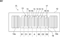
- FIG. 2 is a plan view of the elastic wave device according to the first embodiment of the present invention.
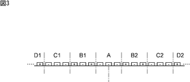
- FIG. 3 is a schematic front view for explaining the first region, the second region, and the third region in the acoustic wave device according to the first embodiment of the present invention.
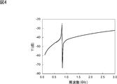
- FIG. 4 is a diagram illustrating the admittance characteristics of the acoustic wave devices of Example 1 and Comparative Example 1.
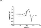
- FIG. 5 is a diagram illustrating the frequency characteristics of third-order harmonic distortion in the elastic wave devices of Example 1 and Comparative Example 1.
- FIG. 6 is a diagram showing IMD characteristics in the acoustic wave devices of Example 1 and Comparative Example 1.
- FIG. 1 is a circuit diagram of a composite filter device having an acoustic wave device according to a first embodiment of the present invention.
- FIG. 2 is a plan view of the elastic wave device according to the first
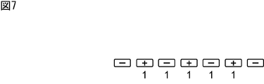
- FIG. 7 is a schematic diagram for explaining the polarity of the electrode finger of the IDT electrode in Comparative Example 1.
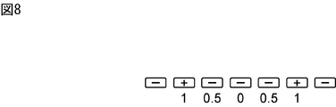
- FIG. 8 is a schematic diagram for explaining the polarities of the electrode fingers of the IDT electrode in the elastic wave device according to the first embodiment.
- FIG. 9 is a schematic diagram for explaining the polarities of the electrode fingers of the IDT electrode in the elastic wave device according to the first embodiment.
- FIG. 10 is a schematic diagram for explaining a main mode elastic wave and a higher-order mode propagation state reflected by reflectors on both sides in the elastic wave device of the first embodiment.
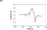
- FIG. 11 is a diagram illustrating the frequency characteristics of the third harmonic distortion of the elastic wave device of Example 2 and the elastic wave device of Comparative Example 1 for the first embodiment.
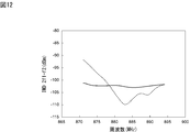
- FIG. 12 is a diagram illustrating IMD characteristics of the elastic wave device of Example 2 and the elastic wave device of Comparative Example 1 according to the first embodiment.
- FIG. 13 is a plan view of an acoustic wave device according to the second embodiment of the present invention.
- FIG. 14 is a diagram illustrating phase characteristics of Example 3 and Comparative Example 2 for the acoustic wave device according to the second embodiment.
- FIG. 15 is a circuit diagram of a notch filter as a band-pass filter using the elastic wave device of the second embodiment.
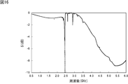
- FIG. 16 is a diagram illustrating pass characteristics of Example 4 and Comparative Example 3 for the notch filter illustrated in FIG. 15.
- FIG. 17 is an enlarged view showing a part of the pass characteristic shown in FIG. FIG.
- FIG. 18 is a schematic plan view showing a first modification of the configuration of the continuous area as the first area.
- FIG. 19 is a schematic plan view showing a second modification of the configuration of the continuous area as the first area.
- FIG. 20 is a schematic plan view showing a modification of the IDT electrode used in the acoustic wave device of the present invention.
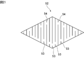
- FIG. 21 is a schematic plan view showing another modification of the IDT electrode used in the acoustic wave device of the present invention.
- FIG. 1 is a circuit diagram of a composite filter device having an elastic wave device according to a first embodiment of the present invention.
- the composite filter device 1 has first to third filters 5 to 7.
- the first to third filters 5 to 7 are band-pass filters, respectively.
- the composite filter device 1 has an antenna terminal 2. One end of first to third filters 5 to 7 is commonly connected to the antenna terminal 2.
- the first filter 5 is a transmission filter.
- the first filter 5 includes a plurality of series arm resonators S1 to S4 and a plurality of parallel arm resonators P1, P2, and P3. Accordingly, the first filter 5 is a ladder-type elastic wave filter.
- the first filter 5 is connected to the transmission terminal 3.
- the second filter 6 is connected to the reception terminal 4.
- the series arm resonators S1 to S4 and the parallel arm resonators P1 to P3 are composed of 1-port type acoustic wave resonators.
- the characteristic of the composite filter device 1 is that, in the first filter 5, the series arm resonators S1 to S4 and the parallel arm resonators P1 to P3 are constituted by the elastic wave device of the present invention. This will be described below as a representative of the series arm resonator S1.
- FIG. 2 is a plan view of the elastic wave device 11 of the first embodiment constituting the series arm resonator S1.
- FIG. 3 is a schematic front view for explaining the first region, the second region, and the third region in the acoustic wave device according to the first embodiment of the present invention.
- the IDT electrode 13 and the reflectors 14 a and 14 b are provided on the piezoelectric substrate 12.
- the elastic wave device 11 is a 1-port elastic wave resonator.
- the elastic wave device has a problem that distortion occurs due to nonlinearity in the IDT electrode.
- the IDT electrode 13 has the following configuration, nonlinearity is improved.
- the IDT electrode 13 has a plurality of first electrode fingers 15 and a plurality of second electrode fingers 16. One end of each of the plurality of first electrode fingers 15 is connected to the first bus bar 17. One end of each of the plurality of second electrode fingers 16 is connected to the second bus bar 18.
- the conventional IDT electrode a plurality of first and second electrode fingers are alternately arranged along the elastic wave propagation direction.
- the three adjacent electrode fingers 15 have the same potential.
- the first electrode finger 15 is connected to the first bus bar 17. That is, in the first region A, adjacent electrode fingers are connected to the same potential.
- Second regions B1 and B2 are provided on both sides of the first region A in the elastic wave propagation direction.
- the first electrode fingers 15 and the second electrode fingers 16 are alternately arranged in the elastic wave propagation direction. Therefore, in the second regions B1 and B2, when an AC electric field is applied between the first and second electrode fingers 15 and 16, an elastic wave is excited.
- Third regions C1 and C2 are provided on the opposite side of the second regions B1 and B2 from the first region A.
- the third regions C1 and C2 as in the first region A, one end of the plurality of first electrode fingers 15 is connected to the first bus bar 17, and the second electrode fingers 16 are arranged. Not. Accordingly, the non-linearity is improved also in the third regions C1 and C2.
- region D1, D2 is provided in the elastic wave propagation direction outer side of 3rd area
- the first electrode fingers 15 and the second electrode fingers 16 are alternately arranged in the elastic wave propagation direction. Therefore, also in the fourth regions D1 and D2, elastic waves are excited during driving.
- the IDT electrode 13 has the first region A and the third regions C1 and C2, nonlinearity is improved. Therefore, distortion hardly occurs during driving.
- a large stress is generated during driving in the central region in the elastic wave propagation direction. That is, since the first region A is a discontinuous portion that does not have the periodic structure of the first and second electrode fingers as described above, the linearity can be improved more effectively. It is said that.
- Example 1 Comparative Example 1 that the non-linearity is improved by the elastic wave device 11 of the first embodiment without causing changes in admittance characteristics and impedance characteristics.
- the elastic wave device 11 of Example 1 was manufactured with the following design parameters. LiNbO 3 was used as the piezoelectric substrate 12. The wavelength ⁇ determined by the electrode finger pitch was 4.6 ⁇ m. The duty of the IDT electrode 13 was 0.5. The total number of electrode fingers of the IDT electrode 13 was 237. The number of electrode fingers in the reflectors 14a and 14b was ten. In the IDT electrode 13, the number of electrode fingers in the first region A is 11, the number of electrode fingers in the second regions B1 and B2 is 51, and the number of electrode fingers in the third regions C1 and C2 is 11. The number of electrode fingers in the fourth region D1, D2 was 51. The electrode finger crossing width was 110 ⁇ m.
- the electrode finger crossing width is 100 ⁇ m, and the first electrode finger and the second electrode finger are alternately arranged in the elastic wave propagation direction also in the first and third regions.
- the elastic wave device of Comparative Example 1 was fabricated in the same manner as in Example 1 above.
- the electrode finger cross width in the elastic wave device of Comparative Example 1 was 100 ⁇ m, whereas in Example 1, the capacitance was different, so the electrode finger cross width was corrected to 110 ⁇ m.
- FIG. 4 shows the admittance characteristics of Example 1 with a solid line and the admittance characteristics of Comparative Example 1 with a broken line. Note that the frequency range between the resonance frequency and the antiresonance frequency in the elastic wave resonator of the first embodiment is 800 MHz to 900 MHz.
- FIG. 5 is a diagram showing the frequency characteristics of third-order harmonic distortion in the elastic wave devices of Example 1 and Comparative Example 1
- FIG. 6 is a diagram showing the IMD characteristics.
- a solid line shows the result of Example 1
- a broken line shows the result of Comparative Example 1.
- the frequency range of the third harmonic appears at 2400 MHz to 2700 MHz.
- IMD 2f1-f2
- f1 825 MHz to 849 MHz
- FIG. 7 is a schematic diagram showing the polarities of a plurality of electrode fingers of the IDT electrode in the elastic wave device of Comparative Example 1.
- FIG. 8 shows the vicinity of the first region A in the elastic wave device 11 of the first embodiment. It is a schematic diagram which shows the polarity of a several electrode finger. 7 and 8, the excitation intensity is schematically represented by “1”, “0.5”, and “0”. That is, the excitation intensity is 1 when the polarities of adjacent electrode fingers are reversed, and 0 when the polarities are the same.
- the polarity of adjacent electrode fingers is reversed, so that the excitation intensity is high, but the nonlinearity is high.
- the polarities of the adjacent electrode fingers are equal, so that the excitation intensity is lowered.
- Linearity is improved.
- the first region A is provided in the center of the elastic wave propagation direction, the linearity can be further effectively improved in the central region where the stress is large.
- the electrode finger on the first region A side of the second region B1 is the second electrode finger 16 and the end of the second region B2 on the first region A side is the second electrode finger 16.
- the electrode finger was also the second electrode finger 16, and both electrode fingers had the same polarity.
- the polarities of the second region B1 and the second region B2 are different for the wave propagating from the second region B1 through the first region A to the second region B2.
- the electrode finger 16 is preferably used, and the electrode finger at the end of the second region B2 on the first region A side is preferably the first electrode finger 15. That is, the polarity of the electrode finger at the end of the second region B1 on the first region A side is different from the polarity of the electrode finger at the end of the second region B2 on the first region A side. preferable.
- the electrode finger at the end of the second region B1 on the first region A side is the second electrode finger 16
- the second The electrode finger at the end of the region B2 on the first region A side is preferably the second electrode finger 16. That is, the polarity of the electrode finger at the end of the second region B1 on the first region A side is the same as the polarity of the electrode finger at the end of the second region B2 on the first region A side. preferable. In any case, harmonics reflected by the reflector and passing through the first region A can be canceled, and better characteristics can be obtained. This will be described with reference to FIG.
- the main mode elastic wave excited in the second region B1 and the main mode elastic wave excited in the second region B2 are shown by arrows in the drawing. Propagate in the direction shown.
- the elastic wave indicated by the arrow A1 is reflected by the region A and returns to the region B1
- the elastic wave indicated by the arrow -A1 is also the same in the region A. Since it is reflected and returns to the region B2, the elastic wave in the main mode is not canceled as a result.
- Example 2 The design parameters of Example 2 were the same as Example 1 except that the polarities of the electrode fingers at the ends of the second regions B1 and B2 on the first region A side were reversed.
- the admittance characteristics of the elastic wave device of Example 2 and the elastic wave device of Comparative Example 1 almost overlapped with the admittance characteristics of Example 1 shown in FIG.
- FIG. 11 is a diagram showing the frequency characteristics of the third harmonic distortion of the elastic wave devices of Example 2 and Comparative Example 1
- FIG. 12 is a diagram showing the IMD characteristics. 11 and 12, the solid line shows the result of Example 2, and the broken line shows the result of Comparative Example 1.
- FIG. 11 it can be seen that the distortion of the third harmonic can be reduced in the second embodiment as compared with the first comparative example.
- FIG. 12 it can be seen that the IMD characteristics can be improved as compared with Comparative Example 1 according to Example 2. That is, the frequency characteristics and IMD characteristics of the third harmonic distortion are improved by improving the linearity of the IDT electrode.
- FIG. 13 is a plan view of an acoustic wave device 31 according to the second embodiment of the present invention.
- a plurality of floating electrode fingers 35 are provided in the first region A and the third regions C1 and C2.
- the floating electrode finger 35 is not electrically connected to the first bus bar 17 or the second bus bar 18. That is, the floating electrode finger 35 is electrically floated. Therefore, for example, in the first region A, a reflector is constituted by a plurality of floating electrode fingers 35. Also in the third regions C1 and C2, a reflector is constituted by a plurality of floating electrode fingers 35.
- the second regions B1, B2 and the fourth regions D1, D2 are configured in the same manner as the elastic wave device 11.
- the first region A and the third regions C1 and C2 are discontinuous portions of the electrode period. That is, in the electrode structure in which the first electrode fingers 15 and the second electrode fingers 16 are alternately arranged, the first region A and the third regions C1 and C2 are discontinuous portions of the periodic structure. Has been. In the first region A and the third regions C1 and C2, since the elastic wave is not excited by the piezoelectric effect, the linearity is enhanced. Therefore, in the acoustic wave device 31, as with the acoustic wave device 11, nonlinearity is improved. As described above, in the present invention, in the first region A and the third regions C1 and C2, nonlinearity may be improved by not connecting the electrode fingers to other potentials.
- FIG. 14 shows the phase characteristics of Example 3 and Comparative Example 2 for the acoustic wave device 31 of the second embodiment.
- Example 3 The design parameters of Example 3 were the same as those of Example 1 except that the first region A and the third regions C1 and C2 were configured as follows.
- First region A 11 floating electrode fingers were arranged.
- Third region C1, C2 11 floating electrode fingers were arranged.
- the polarity of the electrode finger at the end of the second region B1 on the first region A side and the polarity of the electrode finger at the end of the second region B2 on the first region A side were made different.
- the polarity of the electrode finger at the end of the fourth region D1 on the third region C1 side was made different from the polarity of the electrode finger at the end of the second region B1 on the third region C1 side.
- the polarity of the electrode finger at the end of the fourth region D2 on the third region C2 side and the polarity of the electrode finger at the end of the second region B2 on the third region C2 side were made different.
- Example 14 the solid line shows the result of Example 3, and the broken line shows the result of Comparative Example 2.
- the resonance frequency was designed to be 2450 MHz.
- Arrows E1 to E3 in FIG. 14 all indicate unnecessary wave responses. Compared to Comparative Example 2, according to Example 3, it can be seen that unnecessary waves indicated by arrows E1 to E3 are effectively suppressed.
- unnecessary waves can be canceled in a plurality of regions. That is, the higher order mode that has entered the second area B2 through the first area A from the second area B1 is canceled out by the higher order mode of the second area B2.
- the higher order mode that has entered the second area B1 through the third area C1 from the fourth area D1 cancels out the higher order mode of the second area B1.
- the higher order mode that has entered the second area B2 through the third area C2 from the fourth area D2 cancels out the higher order mode of the second area B2. Therefore, unnecessary waves are effectively suppressed.
- FIG. 15 is a circuit diagram of a notch filter as a second embodiment of the present invention.
- the notch filter 41 is a low-pass filter having inductances L1 and L2 provided on the series arm and electrostatic capacitance provided on the parallel arm.
- a part of the capacitance provided in the parallel arm is replaced by the resonators R1 and R2.
- 2.4 GHz which is the resonance frequency of the resonators R1 and R2
- a steep attenuation characteristic is obtained. Thereby, it is possible to pass a signal in a frequency band of 2.5 GHz to 3.3 GHz.
- the capacitances in the resonators R1 and R2 are C1a and C2a, respectively.
- the inductance values of the inductances L1 and L2 are L1a and L2a.
- Example 4 and Comparative Example 3 as examples of the second embodiment were produced with the following parameters.
- Example 4 L1a and L2a were 1.5 nH, and C1a and C2a were 1.5 pF.
- the resonators R1 and R2 are configured by the elastic wave device 31 of the third embodiment.
- L1a and L2a were each 1.5 nH, and C1a and C2a were each 1.5 pF.
- the resonators R1 and R2 were the same as the acoustic wave device 31 of Example 3 except that the resonators R1 and R2 were configured as follows.
- the polarity of the electrode finger at the end of the second region B1 on the first region A side is the same as the polarity of the electrode finger at the end of the second region B2 on the first region A side. .
- the polarity of the electrode finger at the end of the fourth region D1 on the third region C1 side is the same as the polarity of the electrode finger at the end of the second region B1 on the third region C1 side. .
- the polarity of the electrode finger at the end of the fourth region D2 on the third region C2 side is the same as the polarity of the electrode finger at the end of the second region B2 on the third region C2 side. .
- FIG. 16 shows the pass characteristics of the notch filters of Example 4 and Comparative Example 3
- FIG. 17 is an enlarged view of a part of FIG. The solid line shows the result of Example 4, and the broken line shows the result of Comparative Example 3.
- adjacent electrode fingers are connected to the same potential
- a plurality of floating electrode fingers are shown, these formation patterns are not particularly limited.
- the space between three adjacent first electrode fingers 15 having the same potential may be metallized. That is, the space between the first electrode fingers 15 on both sides in the elastic wave propagation direction may be formed of a metal film.
- the first region may be configured by only one floating electrode finger 35.
- the space between the adjacent floating electrode fingers 35 may be metallized in the first region.
- the space between the floating electrode fingers 35 on both sides in the elastic wave propagation direction is formed of a metal film.
- some of the floating electrode fingers may be electrically connected at the end in the cross width direction. 18 and 19, the excitation intensity in the floating electrode 35 is shown as x1.
- the electrode fingers preferably have different polarities, but may have the same polarity.
- the IDT electrode 51 may be subjected to intersection width weighting. Furthermore, as with the IDT electrode 52 shown in FIG. 21, the intersection width is weighted, and the bus bar may be inclined with respect to the elastic wave propagation direction. Further, like the IDT electrode 52, first and second dummy electrode fingers 53 and 54 may be provided.
- the piezoelectric material layer for exciting the elastic wave is not particularly limited, such as lithium tantalate, lithium niobate, and quartz.
Landscapes
- Physics & Mathematics (AREA)
- Acoustics & Sound (AREA)
- Surface Acoustic Wave Elements And Circuit Networks Thereof (AREA)
Abstract
非線形性が改善された弾性波装置を提供する。 圧電性基板12上に、IDT電極13が設けられており、IDT電極13が、複数本の第1の電極指15と、複数本の第1の電極指15とは異なる電位に接続される複数本の第2の電極指16とを有し、第1,第2の電極指15,16の延びる方向と直交する方向が弾性波伝搬方向であり、IDT電極13が、弾性波伝搬方向中央に設けられた第1の領域Aと、弾性波伝搬方向において第1の領域Aの一方側及び他方側に設けられた第2の領域B1,B2と、弾性波伝搬方向において第2の領域B1,B2の前記第1の領域Aとは反対側に設けられた第3の領域C1,C2を有し、各第2の領域B1,B2において、第1の電極指15と第2の電極指16とが弾性波伝搬方向において交互に配置されており、第1の領域A及び第3の領域C1,C2では、弾性波伝搬方向に沿って隣り合う電極指の電位が同一もしくは電極指が電位に接続されていない、弾性波装置11。
Description
本発明は、圧電性基板上にIDT電極が設けられている弾性波装置、該弾性波装置を有するフィルタ及び複合フィルタ装置に関する。
従来、携帯電話機やスマートフォンのRF段において、弾性波装置を利用した複数のフィルタが用いられている。この種のフィルタでは、弾性波共振子からなる複数の弾性波装置が接続されている。下記の特許文献1には、このような弾性波装置として用いられる弾性波共振子の一例が示されている。特許文献1に記載の弾性波装置では、圧電基板上に、IDT電極及び一対の反射器が設けられている。IDT電極では、複数本の第1の電極指と、第1の電極指と異なる電位に接続される複数本の第2の電極指とが弾性波伝搬方向において交互に配置されている。すなわち、弾性波伝搬方向に沿って隣り合う電極指の電位が異なるように、複数本の電極指が周期的に配置されている。
IDT電極において、複数本の第1の電極指と複数本の第2の電極指との間に交流電界を印加することにより、弾性波が励振される。もっとも、弾性波装置では、電位に接続される電極指が交互に配置されているため、非線形性により物的な歪が生じる。そのため、弾性波装置の特性が劣化することがある。また、このような弾性波装置を用いたフィルタを含む複数のフィルタがアンテナ端側で共通接続されている場合、フィルタの特性の劣化が生じることがある。すなわち、1つのフィルタにおいて、上記非線形性による相互変調歪(IMD)や、高調波歪が生じると、他のフィルタに悪影響を及ぼすことがあった。特に、送信フィルタにおいて、アンテナに最も近い弾性波共振子の非線形性歪が大きいと、受信フィルタなどの他のフィルタの特性に悪影響を及ぼすことがあった。なお、弾性波共振子の線形性を高めるには、電極指交差幅×対数を大きくすることが知られているが、この場合には、弾性波共振子のインピーダンス特性(アドミタンス特性)が変わる。弾性波共振子を用いた弾性波装置で所望のフィルタ特性を得るために、アドミタンス特性を変えずに非線形性を改善することのできる弾性波共振子が求められていた。
本発明の目的は、非線形性が改善された弾性波装置、該弾性波装置を有するフィルタ及び複合フィルタ装置を提供することにある。
本発明に係る弾性波装置は、圧電性基板と、前記圧電性基板上に設けられたIDT電極とを備え、前記IDT電極が、複数本の第1の電極指と、前記複数本の第1の電極指とは異なる電位に接続される複数本の第2の電極指とを有し、前記第1,第2の電極指の延びる方向と直交する方向が弾性波伝搬方向であり、前記IDT電極が弾性波伝搬方向中央に設けられた第1の領域と、前記弾性波伝搬方向において前記第1の領域の一方側及び他方側に設けられた第2の領域と、前記弾性波伝搬方向において、各前記第2の領域の前記第1の領域とは反対側に設けられた第3の領域を有し、前記第2の領域において、前記第1の電極指と前記第2の電極指とが前記弾性波伝搬方向において交互に配置されており、前記第1の領域及び前記第3の領域では、前記弾性波伝搬方向に沿って隣り合う電極指の電位が同一もしくは電極指が電位に接続されていない。
本発明に係る弾性波装置のある特定の局面では、前記第1の領域及び前記第3の領域において、前記弾性波伝搬方向に沿って隣り合う電極指が同電位とされている。この場合、前記第1の領域及び前記第3の領域の少なくとも一方において、前記電極指よりも弾性波伝搬方向に沿う幅方向寸法が大きい、太幅電極指を有していてもよい。
本発明に係る弾性波装置の他の特定の局面では、前記第1の領域及び前記第3の領域の少なくとも一方が、電位に接続されていない浮き電極指からなる。
本発明に係る弾性波装置のさらに他の特定の局面では、2つの前記第2の領域において、前記第1の領域側の端部の前記電極指が同電位に接続される。
本発明に係る弾性波装置の別の特定の局面では、2つの前記第2の領域において、前記第1の領域側の端部の前記電極指が異なる電位に接続される。
本発明に係る弾性波装置のさらに別の特定の局面では、前記第1の領域の前記電極指が奇数本であり、2つの前記第2の領域において、前記第1の領域側の端部の前記電極指の極性が互いに異なっている。
本発明に係る弾性波装置のさらに別の特定の局面では、前記第1の領域の前記電極指が偶数本であり、2つの前記第2の領域において、前記第1の領域側の端部の前記電極指の極性が互いに同じである。
本発明に係るフィルタは、弾性波共振子からなる複数の弾性波装置を有するフィルタであって、前記複数の弾性波装置のうち、少なくとも1つの弾性波装置が、圧電性基板と、前記圧電性基板上に設けられたIDT電極とを備え、前記IDT電極が、複数本の第1の電極指と、前記複数本の第1の電極指とは異なる電位に接続される複数本の第2の電極指とを有し、前記第1,第2の電極指の延びる方向と直交する方向が弾性波伝搬方向であり、前記IDT電極が前記弾性波伝搬方向中央に設けられた第1の領域と、前記弾性波伝搬方向において前記第1の領域の一方側及び他方側に設けられた第2の領域と、前記弾性波伝搬方向において、各前記第2の領域の前記第1の領域とは反対側に設けられた第3の領域を有し、前記第2の領域において、前記第1の電極指と前記第2の電極指とが前記弾性波伝搬方向において交互に配置されており、前記第1の領域及び前記第3の領域では、前記弾性波伝搬方向に沿って隣り合う電極指の電位が同一もしくは電極指が電位に接続されていない。
本発明に係る複合フィルタ装置は、n個のフィルタを備え、前記n個のフィルタの一端が共通接続されており、前記n個のフィルタのうち少なくとも1つのフィルタが、本発明に従って構成された弾性波装置を有する。
本発明に係る複合フィルタ装置のある特定の局面では、n個のフィルタと、前記n個のフィルタの一端が共通接続されているアンテナ端子と、を備え、前記n個のフィルタのうち少なくとも1つのフィルタが、少なくとも1つの弾性波装置を有し、前記フィルタにおいて、前記アンテナ端子に最も近い前記弾性波装置が、本発明に従って構成された弾性波装置からなる。
本発明に係る弾性波装置によれば、非線形性を改善することができる。従って、本発明に係る弾性波装置を用いた本発明に係るフィルタ及び複合フィルタ装置によれば、電気的特性の劣化が生じ難く、かつ他のフィルタのフィルタ特性の劣化が生じ難い。
以下、図面を参照しつつ、本発明の具体的な実施形態を説明することにより、本発明を明らかにする。
なお、本明細書に記載の各実施形態は、例示的なものであり、異なる実施形態間において、構成の部分的な置換または組み合わせが可能であることを指摘しておく。
図1は、本発明の第1の実施形態の弾性波装置を有する複合フィルタ装置の回路図である。
複合フィルタ装置1は、第1~第3のフィルタ5~7を有する。本実施形態では、第1~第3のフィルタ5~7は、それぞれ、帯域通過型フィルタである。
複合フィルタ装置1は、アンテナ端子2を有する。アンテナ端子2に、第1~第3のフィルタ5~7の一端が共通接続されている。第1のフィルタ5は、送信フィルタである。第1のフィルタ5は、複数の直列腕共振子S1~S4及び複数の並列腕共振子P1,P2,P3を有する。第1のフィルタ5は、従って、ラダー型の弾性波フィルタである。第1のフィルタ5は、送信端子3に接続されている。第2のフィルタ6は受信端子4に接続されている。
直列腕共振子S1~S4及び並列腕共振子P1~P3は、1ポート型弾性波共振子からなる。
複合フィルタ装置1の特徴は、第1のフィルタ5において、直列腕共振子S1~S4及び並列腕共振子P1~P3が、本発明の弾性波装置により構成されていることにある。これを、直列腕共振子S1を代表して以下において説明する。
図2は、直列腕共振子S1を構成している第1の実施形態の弾性波装置11の平面図である。図3は、本発明の第1の実施形態の弾性波装置における第1の領域、第2の領域及び第3の領域を説明するための模式的正面図である。弾性波装置11では、圧電性基板12上に、IDT電極13及び反射器14a,14bが設けられている。弾性波装置11は、1ポート型弾性波共振子である。前述したように、弾性波装置では、IDT電極における非線形性により歪が生じるという問題があった。これに対して、弾性波装置11では、IDT電極13が、以下の構成を備えるため、非線形性が改善されている。
IDT電極13は、複数本の第1の電極指15と、複数本の第2の電極指16とを有する。複数本の第1の電極指15は、第1のバスバー17に一端が接続されている。複数本の第2の電極指16は、第2のバスバー18に一端が接続されている。
ところで、前述したように、従来のIDT電極では、複数本の第1,第2の電極指が、弾性波伝搬方向に沿って、交互に配置されていた。これに対して、IDT電極13では、図2に示すように、弾性波伝搬方向中央に位置する第1の領域Aにおいて、隣り合う第1の電極指15が同電位となるように、3本の第1の電極指15が第1のバスバー17に接続されている。すなわち、第1の領域Aにおいては、隣り合う電極指は同電位に接続されていることになる。
第1の領域Aの弾性波伝搬方向両側に第2の領域B1,B2が設けられている。第2の領域B1,B2では、第1の電極指15と第2の電極指16とが弾性波伝搬方向において交互に配置されている。従って、第2の領域B1,B2では、第1,第2の電極指15,16間に交流電界を印加した場合、弾性波が励振される。
第2の領域B1,B2の第1の領域Aとは反対側に、第3の領域C1,C2が設けられている。第3の領域C1,C2では、第1の領域Aと同様に、複数本の第1の電極指15の一端が第1のバスバー17に接続されており、第2の電極指16は配置されていない。従って、第3の領域C1,C2においても、非線形性が改善されている。
第3の領域C1,C2の弾性波伝搬方向外側には、第4の領域D1,D2が設けられている。第4の領域D1,D2においては、第1の電極指15と第2の電極指16とが弾性波伝搬方向において交互に配置されている。従って、第4の領域D1,D2においても、駆動に際し弾性波が励振される。
弾性波装置11では、IDT電極13が、上記第1の領域A及び第3の領域C1,C2を有するため、非線形性が改善されている。そのため、駆動に際し、歪が生じ難い。特に、IDT電極13においては、弾性波伝搬方向における中央領域において、駆動に際し大きな応力が生じる。すなわち、第1の領域Aが、上記のように、第1,第2の電極指の周期的構造を有しない不連続部分とされていることにより、線形性をより効果的に高めることが可能とされている。
上記第1の実施形態の弾性波装置11によりアドミタンス特性やインピーダンス特性の変化をもたらすことなく、非線形性が改善されることを、以下の実施例1及び比較例1を参照して説明する。
以下の設計パラメータで、実施例1の弾性波装置11を作製した。圧電性基板12として、LiNbO3を用いた。電極指ピッチで定まる波長λは4.6μmとした。IDT電極13におけるデューティは、0.5とした。IDT電極13の電極指の本数は、全体で237本とした。反射器14a,14bにおける電極指の本数は10本とした。IDT電極13において、第1の領域Aの電極指の本数は11本、第2の領域B1,B2における電極指の本数は、51本、第3の領域C1,C2における電極指の本数は11本、第4の領域D1,D2における電極指の本数は51本とした。また、電極指交差幅は110μmとした。
比較のために、電極指交差幅は100μmであり、第1,第3の領域においても、第1の電極指と第2の電極指とが弾性波伝搬方向において交互に配置されていることを除いては、上記実施例1と同様にして比較例1の弾性波装置を作製した。なお、比較例1の弾性波装置における電極指交差幅が100μmであるのに対し、実施例1では、容量が異なるため、電極指交差幅を110μmと補正した。
図4に実線で実施例1のアドミタンス特性を、破線で比較例1のアドミタンス特性を示す。なお、上記実施例1の弾性波共振子における共振周波数と反共振周波数との間の周波数域は800MHz~900MHzである。
図4から明らかなように、実線と破線がほぼ重なっており、実施例1の弾性波装置11では、比較例1の弾性波装置と共振特性がほとんど変わらないことがわかる。
図5は、実施例1及び比較例1の弾性波装置における3次高調波歪の周波数特性を示す図であり、図6は、IMD特性を示す図である。実線が実施例1の結果を、破線が比較例1の結果を示す。図5及び図6から明らかなように、比較例1に比べ、実施例1によれば、3次高調波歪を小さくすることができ、かつIMD特性も改善されていることがわかる。
なお、3次高調波の周波数域は、2400MHz~2700MHzに現れている。
また、IMD=2f1-f2において、f1=825MHz~849MHzとし、f2=870MHz~894MHzとした。従って、2f1-f2=780MHz~804MHzである。
上記のように、弾性波装置11において、非線形性が改善されるメカニズムを、図7及び図8を参照して説明する。
図7は、比較例1の弾性波装置におけるIDT電極の複数本の電極指の極性を示す模式図である、図8は第1の実施形態の弾性波装置11における第1の領域A付近の複数本の電極指の極性を示す模式図である。図7及び図8では、励振強度を、「1」、「0.5」、「0」で模式的に表す。すなわち、隣り合う電極指の極性が反転している場合、励振強度は1であり、同極性の場合には、0となる。図7に示すように、比較例1の弾性波装置では、隣り合う電極指の極性が反転しているため、励振強度は高いが、非線形性が高くなっている。これに対して、図8に示すように、第1の実施形態では、第1の領域Aにおいて、隣り合う電極指の極性が等しくなっているため、励振強度が低められているが、それによって線形性が高められている。しかも、弾性波伝搬方向中央に第1の領域Aが設けられているため、応力が大きい中央領域において、線形性をより一層効果的に改善することが可能とされている。
なお、弾性波装置11では、第2の領域B1の第1の領域A側の電極指は、第2の電極指16であり、第2の領域B2の第1の領域A側の端部の電極指も第2の電極指16であり、両電極指が同極性であった。
もっとも、第2の領域B1から第1の領域Aを通過して第2の領域B2に伝搬する波にとって、第2の領域B1と第2の領域B2の極性が異なっていることが好ましい。図9に示すように、第1の領域AのIDT電極の電極指の本数が奇数本である場合は、第2の領域B1の第1の領域A側の端部の電極指を第2の電極指16とし、第2の領域B2の第1の領域A側の端部の電極指を第1の電極指15とすることが望ましい。すなわち、第2の領域B1の第1の領域A側の端部の電極指の極性と、第2の領域B2の第1の領域A側の端部の電極指の極性が異なっていることが好ましい。第1の領域AのIDT電極の電極指の本数が偶数本である場合は、第2の領域B1の第1の領域A側の端部の電極指を第2の電極指16とし、第2の領域B2の第1の領域A側の端部の電極指を第2の電極指16とすることが望ましい。すなわち、第2の領域B1の第1の領域A側の端部の電極指の極性と、第2の領域B2の第1の領域A側の端部の電極指の極性が同じであることが好ましい。いずれの場合にも、反射器で反射され、第1の領域Aを通過してきた高調波を相殺し、より良好な特性を得ることができる。これを、図10を参照して説明する。
図10に示すように、IDT電極13を駆動すると、第2の領域B1で励振されたメインモードの弾性波と、第2の領域B2で励振されたメインモードの弾性波とが図示の矢印で示す方向に伝搬する。この場合、IDT電極13におけるメインモードの弾性波の反射係数が大きいため、矢印A1で示す弾性波は領域Aで反射されて領域B1に戻り、矢印-A1で示す弾性波も同様に領域Aで反射され領域B2に戻るので、結果として、メインモードの弾性波は相殺されない。これに対して、高次モードについては、矢印B1aで示す高次モードと、矢印-B1aで示す高次モードが、それぞれ矢印方向に伝搬するが、IDT電極13における高次モードの反射係数が小さいため、それぞれの高次モードは領域Aを通過し、両者が逆相となる。そのため、高次モードの応答を効果的に抑制することができる。このように、第2の領域B1から第1の領域Aを通過して第2の領域B2に伝搬する波にとって、第2の領域B1と第2の領域B2の極性を異ならせることが望ましい。このような望ましい弾性波装置についての実施例2及び比較例1について、図11及び図12を参照して説明する。
実施例2の設計パラメータは、第2の領域B1,B2の第1の領域A側の端部の電極指の極性を逆極性としたことを除いては、実施例1と同様とした。実施例2の弾性波装置及び比較例1の弾性波装置のアドミタンス特性は、図4に示した実施例1のアドミタンス特性とほぼ重なっていた。他方、図11は、実施例2及び比較例1の弾性波装置の3次高調波歪の周波数特性を示す図であり、図12はIMD特性を示す図である。図11及び図12において、実線が実施例2の結果を、破線が比較例1の結果を示す。図11から明らかなように、実施例2においても、比較例1に比べて、3次高調波の歪を小さくし得ることがわかる。また、図12に示すように、IMD特性についても、実施例2によれば、比較例1に比べて改善され得ることがわかる。すなわち、IDT電極における線形性の向上により、3次高調波歪の周波数特性及びIMD特性が改善されている。
(第2の実施形態)
図13は、本発明の第2の実施形態に係る弾性波装置31の平面図である。弾性波装置31では、第1の領域A、第3の領域C1,C2において、複数本の浮き電極指35が設けられている。浮き電極指35は、第1のバスバー17にも、第2のバスバー18にも電気的に接続されていない。すなわち、浮き電極指35は、電気的に浮かされている。従って、例えば第1の領域Aにおいては、複数本の浮き電極指35により、反射器が構成されている。第3の領域C1,C2においても、複数本の浮き電極指35により反射器が構成されている。
図13は、本発明の第2の実施形態に係る弾性波装置31の平面図である。弾性波装置31では、第1の領域A、第3の領域C1,C2において、複数本の浮き電極指35が設けられている。浮き電極指35は、第1のバスバー17にも、第2のバスバー18にも電気的に接続されていない。すなわち、浮き電極指35は、電気的に浮かされている。従って、例えば第1の領域Aにおいては、複数本の浮き電極指35により、反射器が構成されている。第3の領域C1,C2においても、複数本の浮き電極指35により反射器が構成されている。
弾性波装置31では、第2の領域B1,B2及び第4の領域D1,D2は、弾性波装置11と同様に構成されている。
弾性波装置31では、IDT電極13において、上記第1の領域A及び第3の領域C1,C2が、電極周期の不連続部分とされている。すなわち、第1の電極指15と第2の電極指16とが交互に配置されている電極構造において、第1の領域A及び第3の領域C1,C2が該周期的構造の不連続部分とされている。そして、第1の領域A及び第3の領域C1,C2においては、圧電効果により弾性波が励振されないため、線形性が高められている。従って、弾性波装置31では、弾性波装置11と同様に、非線形性が改善されている。このように、本発明においては、上記第1の領域A及び第3の領域C1,C2においては、電極指が他の電位に接続されていないことによって、非線形性が改善されてもよい。
上記第2の実施形態の弾性波装置31についての実施例3及び比較例2の位相特性を図14に示す。
なお、実施例3の設計パラメータとしては、第1の領域A及び第3の領域C1,C2において、以下のように構成したことを除いては、実施例1と同様とした。
第1の領域A:浮き電極指を11本配置した。
第3の領域C1,C2:浮き電極指を11本配置した。
第2の領域B1の第1の領域A側の端部の電極指の極性と、第2の領域B2の第1の領域A側の端部の電極指の極性を異ならせた。
第4の領域D1の第3の領域C1側の端部の電極指の極性と、第2の領域B1の第3の領域C1側の端部の電極指の極性を異ならせた。
第4の領域D2の第3の領域C2側の端部の電極指の極性と、第2の領域B2の第3の領域C2側の端部の電極指の極性を異ならせた。
図14において、実線が実施例3の結果を示し、破線が比較例2の結果を示す。なお、実施例3においては、共振周波数は2450MHzとなるように設計した。図14における矢印E1~E3は、全て不要波の応答を示す。比較例2に比べ、実施例3によれば、矢印E1~E3で示す不要波が効果的に抑制されていることがわかる。上記構成を取ることで、複数領域で不要波の相殺が実現できる。すなわち、第2の領域B1から第1の領域Aを通過して第2の領域B2に入った高次モードは第2の領域B2の高次モードと相殺される。第4の領域D1から第3の領域C1を通過して第2の領域B1に入った高次モードは第2の領域B1の高次モードと相殺される。第4の領域D2から第3の領域C2を通過して第2の領域B2に入った高次モードは第2の領域B2の高次モードと相殺される。よって、不要波が効果的に抑制される。
図15は、本発明の第2の実施形態としてのノッチフィルタの回路図である。ノッチフィルタ41は、直列腕に設けられたインダクタンスL1,L2と、並列腕に設けられた静電容量とを有する、ローパスフィルタである。ここでは、並列腕に設けられた静電容量の一部が、共振子R1,R2で置換されている。共振子R1,R2の共振周波数である2.4GHz付近において、急峻な減衰特性が得られるように構成されている。それによって、2.5GHz~3.3GHzの周波数帯の信号を通過させることが可能とされている。なお、共振子R1,R2における静電容量を、それぞれ、C1a,C2aとする。また、インダクタンスL1,L2のインダクタンス値を、L1a,L2aとする。
第2の実施形態についての実施例としての実施例4及び比較例3を、以下のパラメータで作製した。
実施例4において、L1a,L2aはそれぞれ1.5nH、C1a,C2aはそれぞれ1.5pFとした。共振子R1,R2は、実施例3の弾性波装置31で構成されている。
比較例3において、L1a,L2aはそれぞれ1.5nH、C1a,C2aはそれぞれ1.5pFとした。共振子R1,R2は、以下のように構成したことを除いては、実施例3の弾性波装置31と同様とした。
第2の領域B1の第1の領域A側の端部の電極指の極性と、第2の領域B2の第1の領域A側の端部の電極指の極性とは、同じとされている。
第4の領域D1の第3の領域C1側の端部の電極指の極性と、第2の領域B1の第3の領域C1側の端部の電極指の極性とは、同じとされている。
第4の領域D2の第3の領域C2側の端部の電極指の極性と、第2の領域B2の第3の領域C2側の端部の電極指の極性とは、同じとされている。
図16は、実施例4及び比較例3のノッチフィルタの通過特性を示し、図17は、図16の一部を拡大して示す図である。なお、実線が実施例4、破線が比較例3の結果を示す。
図16及び図17から、実施例4によれば、通過帯域である、2.7GHz~3.3GHz付近において、不要波による局所的な挿入損失の劣化を大幅に小さくし得ることがわかる。
上記第1の実施形態及び第2の実施形態では、第1の領域Aや、第3の領域C1,C2において、中期の不連続部分として、隣り合う電極指が同電位に接続される構成や、複数の浮き電極指を示したが、これらの形成パターンについては、特に限定されない。例えば、図2において、同電位となる3本の隣り合う第1の電極指15間をメタライズしてもよい。すなわち、弾性波伝搬方向両側の第1の電極指15間が、金属膜で構成されていてもよい。この場合、IDT電極13において最大の電極指幅を有する電極指であって、当該電極指を除く電極指における平均電極指幅の2倍以上の電極指幅を有する太幅電極指(塗りつぶし電極)となる。また、図18に示す第1の変形例のように、一本の浮き電極指35のみで第1の領域を構成してもよい。また、図19に示す、第2の変形例のように、第1の領域において、隣り合う浮き電極指35間をメタライズしてもよい。この場合、図19に示す図は、弾性波伝搬方向両側の浮き電極指35間が金属膜で構成されることになる。また、複数の浮き電極指の少なくとも一部の浮き電極指の電位を同一とするため、一部の浮き電極指間が交差幅方向の端部にて電気的に接続されていてもよい。なお、図18及び図19において、浮き電極35における励振強度をx1として示す。
また、第1,第2の実施形態及び図18及び図19に示した各構成において、第1の領域Aに対し、両側の第2の領域B1,B2の第1の領域A側の端部の電極指は、前述したように、異なる極性であることが好ましいが、同極性であってもよい。
また、図20に示すように、IDT電極51において、交差幅重み付けが施されていてもよい。さらに、図21に示すIDT電極52のように、交差幅重み付けが施されており、さらにバスバーが弾性波伝搬方向に対して傾斜していてもよい。また、IDT電極52のように、第1,第2のダミー電極指53,54が設けられているものであってもよい。
また、弾性波を励振する圧電材料層としては、リチウムタンタレート、リチウムナイオベート、水晶など特に限定されない。また、高次モードの発生しやすい圧電材料層上に、酸化シリコン、窒化シリコン等の誘電膜を形成した積層構造、圧電材料層をシリコンやアルミナ、サファイア等の支持基板に貼り付けた積層構造であってもよい。
1…複合フィルタ装置
2…アンテナ端子
3…送信端子
4…受信端子
5~7…第1~第3のフィルタ
11…弾性波装置
12…圧電性基板
13…IDT電極
14a,14b…反射器
15,16…第1,第2の電極指
17,18…第1,第2のバスバー
31…弾性波装置
35…浮き電極指
41…ノッチフィルタ
51…IDT電極
52…IDT電極
53,54…第1,第2のダミー電極指
P1~P3…並列腕共振子
S1~S4…直列腕共振子
2…アンテナ端子
3…送信端子
4…受信端子
5~7…第1~第3のフィルタ
11…弾性波装置
12…圧電性基板
13…IDT電極
14a,14b…反射器
15,16…第1,第2の電極指
17,18…第1,第2のバスバー
31…弾性波装置
35…浮き電極指
41…ノッチフィルタ
51…IDT電極
52…IDT電極
53,54…第1,第2のダミー電極指
P1~P3…並列腕共振子
S1~S4…直列腕共振子
Claims (11)
- 圧電性基板と、前記圧電性基板上に設けられたIDT電極とを備え、
前記IDT電極が、複数本の第1の電極指と、前記複数本の第1の電極指とは異なる電位に接続される複数本の第2の電極指とを有し、
前記第1,第2の電極指の延びる方向と直交する方向が弾性波伝搬方向であり、
前記IDT電極が弾性波伝搬方向中央に設けられた第1の領域と、前記弾性波伝搬方向において前記第1の領域の一方側及び他方側に設けられた第2の領域と、前記弾性波伝搬方向において、各前記第2の領域の前記第1の領域とは反対側に設けられた第3の領域を有し、前記第2の領域において、前記第1の電極指と前記第2の電極指とが前記弾性波伝搬方向において交互に配置されており、前記第1の領域及び前記第3の領域では、前記弾性波伝搬方向に沿って隣り合う電極指の電位が同一もしくは電極指が電位に接続されていない、弾性波装置。 - 前記第1の領域及び前記第3の領域において、前記弾性波伝搬方向に沿って隣り合う電極指が同電位とされている、請求項1に記載の弾性波装置。
- 前記第1の領域及び前記第3の領域の少なくとも一方において、前記電極指よりも弾性波伝搬方向に沿う幅方向寸法が大きい、太幅電極指を有する、請求項2に記載の弾性波装置。
- 前記第1の領域及び前記第3の領域の少なくとも一方が、電位に接続されていない浮き電極指からなる、請求項1に記載の弾性波装置。
- 2つの前記第2の領域において、前記第1の領域側の端部の前記電極指が同電位に接続される、請求項1~4のいずれか1項に記載の弾性波装置。
- 2つの前記第2の領域において、前記第1の領域側の端部の前記電極指が異なる電位に接続される、請求項1~4のいずれか1項に記載の弾性波装置。
- 前記第1の領域の前記電極指が奇数本であり、2つの前記第2の領域において、前記第1の領域側の端部の前記電極指の極性が互いに異なっている、請求項1~4のいずれか1項に記載の弾性波装置。
- 前記第1の領域の前記電極指が偶数本であり、2つの前記第2の領域において、前記第1の領域側の端部の前記電極指の極性が互いに同じである、請求項1~4のいずれか1項に記載の弾性波装置。
- 弾性波共振子からなる複数の弾性波装置を有するフィルタであって、
前記複数の弾性波装置のうち、少なくとも1つの弾性波装置が、圧電性基板と、前記圧電性基板上に設けられたIDT電極とを備え、
前記IDT電極が、複数本の第1の電極指と、前記複数本の第1の電極指とは異なる電位に接続される複数本の第2の電極指とを有し、
前記第1,第2の電極指の延びる方向と直交する方向が弾性波伝搬方向であり、
前記IDT電極が前記弾性波伝搬方向中央に設けられた第1の領域と、前記弾性波伝搬方向において前記第1の領域の一方側及び他方側に設けられた第2の領域と、前記弾性波伝搬方向において、各前記第2の領域の前記第1の領域とは反対側に設けられた第3の領域を有し、前記第2の領域において、前記第1の電極指と前記第2の電極指とが前記弾性波伝搬方向において交互に配置されており、前記第1の領域及び前記第3の領域では、前記弾性波伝搬方向に沿って隣り合う電極指の電位が同一もしくは電位に接続されていない、フィルタ。 - n個のフィルタを備え、前記n個のフィルタの一端が共通接続されており、
前記n個のフィルタのうち少なくとも1つのフィルタが、請求項1~8のいずれか1項に記載の弾性波装置を有する、複合フィルタ装置。 - n個のフィルタと、
前記n個のフィルタの一端が共通接続されているアンテナ端子と、
を備え
前記n個のフィルタのうち少なくとも1つのフィルタが、少なくとも1つの弾性波装置を有し、前記フィルタにおいて、前記アンテナ端子に最も近い前記弾性波装置が、請求項1~8のいずれか1項に記載の弾性波装置からなる、複合フィルタ装置。
Priority Applications (2)
| Application Number | Priority Date | Filing Date | Title |
|---|---|---|---|
| CN201880027238.XA CN110582937B (zh) | 2017-04-28 | 2018-04-24 | 弹性波装置、滤波器以及复合滤波器装置 |
| US16/658,211 US11165409B2 (en) | 2017-04-28 | 2019-10-21 | Acoustic wave device, filter, and composite filter device |
Applications Claiming Priority (4)
| Application Number | Priority Date | Filing Date | Title |
|---|---|---|---|
| JP2017090499 | 2017-04-28 | ||
| JP2017-090499 | 2017-04-28 | ||
| JP2017-126121 | 2017-06-28 | ||
| JP2017126121 | 2017-06-28 |
Related Child Applications (1)
| Application Number | Title | Priority Date | Filing Date |
|---|---|---|---|
| US16/658,211 Continuation US11165409B2 (en) | 2017-04-28 | 2019-10-21 | Acoustic wave device, filter, and composite filter device |
Publications (1)
| Publication Number | Publication Date |
|---|---|
| WO2018199070A1 true WO2018199070A1 (ja) | 2018-11-01 |
Family
ID=63918355
Family Applications (1)
| Application Number | Title | Priority Date | Filing Date |
|---|---|---|---|
| PCT/JP2018/016562 Ceased WO2018199070A1 (ja) | 2017-04-28 | 2018-04-24 | 弾性波装置、フィルタ及び複合フィルタ装置 |
Country Status (3)
| Country | Link |
|---|---|
| US (1) | US11165409B2 (ja) |
| CN (1) | CN110582937B (ja) |
| WO (1) | WO2018199070A1 (ja) |
Cited By (1)
| Publication number | Priority date | Publication date | Assignee | Title |
|---|---|---|---|---|
| WO2023048280A1 (ja) * | 2021-09-27 | 2023-03-30 | 株式会社村田製作所 | フィルタ装置 |
Families Citing this family (4)
| Publication number | Priority date | Publication date | Assignee | Title |
|---|---|---|---|---|
| WO2018216417A1 (ja) * | 2017-05-26 | 2018-11-29 | 株式会社村田製作所 | 弾性波装置、フィルタ、高周波フロントエンド回路及び通信装置 |
| JP2020123819A (ja) * | 2019-01-30 | 2020-08-13 | 株式会社村田製作所 | 弾性波フィルタ |
| WO2021117581A1 (ja) * | 2019-12-09 | 2021-06-17 | 株式会社村田製作所 | 弾性波装置 |
| US11784627B2 (en) * | 2021-02-01 | 2023-10-10 | Vanguard International Semiconductor Corporation | Lamb wave resonator and method of fabricating the same |
Citations (6)
| Publication number | Priority date | Publication date | Assignee | Title |
|---|---|---|---|---|
| JPH05145367A (ja) * | 1991-02-07 | 1993-06-11 | Mitsubishi Electric Corp | 弾性表面波装置 |
| JPH08330897A (ja) * | 1995-05-29 | 1996-12-13 | Sanyo Electric Co Ltd | 弾性表面波フィルタ |
| JP2000315931A (ja) * | 1999-04-28 | 2000-11-14 | Murata Mfg Co Ltd | Saw共振子、複合sawフィルタ及びsawフィルタ |
| JP2002319842A (ja) * | 2001-04-20 | 2002-10-31 | Fujitsu Ltd | 弾性表面波共振子及び弾性表面波フィルタ |
| JP2005303893A (ja) * | 2004-04-15 | 2005-10-27 | Seiko Epson Corp | 共振子型sawフィルタ |
| JP2014229916A (ja) * | 2013-05-17 | 2014-12-08 | 京セラ株式会社 | 弾性表面波素子 |
Family Cites Families (2)
| Publication number | Priority date | Publication date | Assignee | Title |
|---|---|---|---|---|
| EP0746095B1 (en) | 1995-05-29 | 2007-02-14 | SANYO ELECTRIC Co., Ltd. | Surface acoustic wave filter |
| JP2011182117A (ja) | 2010-02-26 | 2011-09-15 | Taiyo Yuden Co Ltd | 弾性波デバイスおよびその製造方法 |
-
2018
- 2018-04-24 CN CN201880027238.XA patent/CN110582937B/zh active Active
- 2018-04-24 WO PCT/JP2018/016562 patent/WO2018199070A1/ja not_active Ceased
-
2019
- 2019-10-21 US US16/658,211 patent/US11165409B2/en active Active
Patent Citations (6)
| Publication number | Priority date | Publication date | Assignee | Title |
|---|---|---|---|---|
| JPH05145367A (ja) * | 1991-02-07 | 1993-06-11 | Mitsubishi Electric Corp | 弾性表面波装置 |
| JPH08330897A (ja) * | 1995-05-29 | 1996-12-13 | Sanyo Electric Co Ltd | 弾性表面波フィルタ |
| JP2000315931A (ja) * | 1999-04-28 | 2000-11-14 | Murata Mfg Co Ltd | Saw共振子、複合sawフィルタ及びsawフィルタ |
| JP2002319842A (ja) * | 2001-04-20 | 2002-10-31 | Fujitsu Ltd | 弾性表面波共振子及び弾性表面波フィルタ |
| JP2005303893A (ja) * | 2004-04-15 | 2005-10-27 | Seiko Epson Corp | 共振子型sawフィルタ |
| JP2014229916A (ja) * | 2013-05-17 | 2014-12-08 | 京セラ株式会社 | 弾性表面波素子 |
Cited By (1)
| Publication number | Priority date | Publication date | Assignee | Title |
|---|---|---|---|---|
| WO2023048280A1 (ja) * | 2021-09-27 | 2023-03-30 | 株式会社村田製作所 | フィルタ装置 |
Also Published As
| Publication number | Publication date |
|---|---|
| US20200052675A1 (en) | 2020-02-13 |
| CN110582937A (zh) | 2019-12-17 |
| CN110582937B (zh) | 2023-08-25 |
| US11165409B2 (en) | 2021-11-02 |
Similar Documents
| Publication | Publication Date | Title |
|---|---|---|
| JP5024373B2 (ja) | 弾性波素子 | |
| JP4798319B1 (ja) | 弾性波装置 | |
| US11165409B2 (en) | Acoustic wave device, filter, and composite filter device | |
| KR101793055B1 (ko) | 래더형 필터 | |
| JP6509151B2 (ja) | 弾性波共振器、フィルタおよびマルチプレクサ | |
| JP6835222B2 (ja) | 弾性波装置及び複合フィルタ装置 | |
| CN107070431B (zh) | 声波谐振器、滤波器和双工器 | |
| WO2014034492A1 (ja) | 弾性波装置及びフィルタ装置 | |
| WO2015002047A1 (ja) | 弾性表面波共振器及び弾性表面波フィルタ装置 | |
| JP2018166340A (ja) | 高周波フィルタ | |
| CN110114973B (zh) | 弹性波装置 | |
| WO2021002321A1 (ja) | 弾性波フィルタおよびマルチプレクサ | |
| JP4727322B2 (ja) | 弾性表面波装置 | |
| JP6750528B2 (ja) | 弾性波フィルタ装置 | |
| JP5045760B2 (ja) | 弾性波フィルタ装置 | |
| KR101974830B1 (ko) | 탄성파 공진자, 탄성파 필터 및 듀플렉서 | |
| JP6585459B2 (ja) | 弾性波素子、分波器および通信装置 | |
| WO2023090172A1 (ja) | 弾性波装置 | |
| CN117981223A (zh) | 弹性波滤波器 | |
| JP6465441B2 (ja) | マルチプレクサ | |
| JP5141776B2 (ja) | 弾性波共振子、ラダー型フィルタ及びデュプレクサ | |
| JP7132841B2 (ja) | 弾性表面波素子、分波器および通信装置 | |
| KR102871957B1 (ko) | 필터 장치 및 멀티플렉서 | |
| WO2024143137A1 (ja) | ラダー型フィルタ | |
| WO2023002948A1 (ja) | 受信フィルタ及び複合フィルタ装置 |
Legal Events
| Date | Code | Title | Description |
|---|---|---|---|
| 121 | Ep: the epo has been informed by wipo that ep was designated in this application |
Ref document number: 18790205 Country of ref document: EP Kind code of ref document: A1 |
|
| NENP | Non-entry into the national phase |
Ref country code: DE |
|
| 122 | Ep: pct application non-entry in european phase |
Ref document number: 18790205 Country of ref document: EP Kind code of ref document: A1 |
|
| NENP | Non-entry into the national phase |
Ref country code: JP |