WO2018190206A1 - 表示装置 - Google Patents
表示装置 Download PDFInfo
- Publication number
- WO2018190206A1 WO2018190206A1 PCT/JP2018/014357 JP2018014357W WO2018190206A1 WO 2018190206 A1 WO2018190206 A1 WO 2018190206A1 JP 2018014357 W JP2018014357 W JP 2018014357W WO 2018190206 A1 WO2018190206 A1 WO 2018190206A1
- Authority
- WO
- WIPO (PCT)
- Prior art keywords
- unit
- signal line
- type
- circuit
- drive circuit
- Prior art date
- Legal status (The legal status is an assumption and is not a legal conclusion. Google has not performed a legal analysis and makes no representation as to the accuracy of the status listed.)
- Ceased
Links
Images






Classifications
-
- G—PHYSICS
- G09—EDUCATION; CRYPTOGRAPHY; DISPLAY; ADVERTISING; SEALS
- G09G—ARRANGEMENTS OR CIRCUITS FOR CONTROL OF INDICATING DEVICES USING STATIC MEANS TO PRESENT VARIABLE INFORMATION
- G09G3/00—Control arrangements or circuits, of interest only in connection with visual indicators other than cathode-ray tubes
- G09G3/20—Control arrangements or circuits, of interest only in connection with visual indicators other than cathode-ray tubes for presentation of an assembly of a number of characters, e.g. a page, by composing the assembly by combination of individual elements arranged in a matrix no fixed position being assigned to or needed to be assigned to the individual characters or partial characters
- G09G3/34—Control arrangements or circuits, of interest only in connection with visual indicators other than cathode-ray tubes for presentation of an assembly of a number of characters, e.g. a page, by composing the assembly by combination of individual elements arranged in a matrix no fixed position being assigned to or needed to be assigned to the individual characters or partial characters by control of light from an independent source
- G09G3/36—Control arrangements or circuits, of interest only in connection with visual indicators other than cathode-ray tubes for presentation of an assembly of a number of characters, e.g. a page, by composing the assembly by combination of individual elements arranged in a matrix no fixed position being assigned to or needed to be assigned to the individual characters or partial characters by control of light from an independent source using liquid crystals
- G09G3/3611—Control of matrices with row and column drivers
- G09G3/3674—Details of drivers for scan electrodes
- G09G3/3677—Details of drivers for scan electrodes suitable for active matrices only
-
- G—PHYSICS
- G02—OPTICS
- G02F—OPTICAL DEVICES OR ARRANGEMENTS FOR THE CONTROL OF LIGHT BY MODIFICATION OF THE OPTICAL PROPERTIES OF THE MEDIA OF THE ELEMENTS INVOLVED THEREIN; NON-LINEAR OPTICS; FREQUENCY-CHANGING OF LIGHT; OPTICAL LOGIC ELEMENTS; OPTICAL ANALOGUE/DIGITAL CONVERTERS
- G02F1/00—Devices or arrangements for the control of the intensity, colour, phase, polarisation or direction of light arriving from an independent light source, e.g. switching, gating or modulating; Non-linear optics
- G02F1/01—Devices or arrangements for the control of the intensity, colour, phase, polarisation or direction of light arriving from an independent light source, e.g. switching, gating or modulating; Non-linear optics for the control of the intensity, phase, polarisation or colour
- G02F1/13—Devices or arrangements for the control of the intensity, colour, phase, polarisation or direction of light arriving from an independent light source, e.g. switching, gating or modulating; Non-linear optics for the control of the intensity, phase, polarisation or colour based on liquid crystals, e.g. single liquid crystal display cells
- G02F1/133—Constructional arrangements; Operation of liquid crystal cells; Circuit arrangements
- G02F1/1333—Constructional arrangements; Manufacturing methods
- G02F1/1345—Conductors connecting electrodes to cell terminals
-
- G—PHYSICS
- G09—EDUCATION; CRYPTOGRAPHY; DISPLAY; ADVERTISING; SEALS
- G09G—ARRANGEMENTS OR CIRCUITS FOR CONTROL OF INDICATING DEVICES USING STATIC MEANS TO PRESENT VARIABLE INFORMATION
- G09G3/00—Control arrangements or circuits, of interest only in connection with visual indicators other than cathode-ray tubes
- G09G3/20—Control arrangements or circuits, of interest only in connection with visual indicators other than cathode-ray tubes for presentation of an assembly of a number of characters, e.g. a page, by composing the assembly by combination of individual elements arranged in a matrix no fixed position being assigned to or needed to be assigned to the individual characters or partial characters
- G09G3/34—Control arrangements or circuits, of interest only in connection with visual indicators other than cathode-ray tubes for presentation of an assembly of a number of characters, e.g. a page, by composing the assembly by combination of individual elements arranged in a matrix no fixed position being assigned to or needed to be assigned to the individual characters or partial characters by control of light from an independent source
- G09G3/36—Control arrangements or circuits, of interest only in connection with visual indicators other than cathode-ray tubes for presentation of an assembly of a number of characters, e.g. a page, by composing the assembly by combination of individual elements arranged in a matrix no fixed position being assigned to or needed to be assigned to the individual characters or partial characters by control of light from an independent source using liquid crystals
- G09G3/3611—Control of matrices with row and column drivers
- G09G3/3685—Details of drivers for data electrodes
- G09G3/3688—Details of drivers for data electrodes suitable for active matrices only
-
- G—PHYSICS
- G02—OPTICS
- G02F—OPTICAL DEVICES OR ARRANGEMENTS FOR THE CONTROL OF LIGHT BY MODIFICATION OF THE OPTICAL PROPERTIES OF THE MEDIA OF THE ELEMENTS INVOLVED THEREIN; NON-LINEAR OPTICS; FREQUENCY-CHANGING OF LIGHT; OPTICAL LOGIC ELEMENTS; OPTICAL ANALOGUE/DIGITAL CONVERTERS
- G02F2201/00—Constructional arrangements not provided for in groups G02F1/00 - G02F7/00
- G02F2201/56—Substrates having a particular shape, e.g. non-rectangular
-
- G—PHYSICS
- G09—EDUCATION; CRYPTOGRAPHY; DISPLAY; ADVERTISING; SEALS
- G09G—ARRANGEMENTS OR CIRCUITS FOR CONTROL OF INDICATING DEVICES USING STATIC MEANS TO PRESENT VARIABLE INFORMATION
- G09G2310/00—Command of the display device
- G09G2310/02—Addressing, scanning or driving the display screen or processing steps related thereto
- G09G2310/0202—Addressing of scan or signal lines
- G09G2310/0221—Addressing of scan or signal lines with use of split matrices
-
- G—PHYSICS
- G09—EDUCATION; CRYPTOGRAPHY; DISPLAY; ADVERTISING; SEALS
- G09G—ARRANGEMENTS OR CIRCUITS FOR CONTROL OF INDICATING DEVICES USING STATIC MEANS TO PRESENT VARIABLE INFORMATION
- G09G2310/00—Command of the display device
- G09G2310/02—Addressing, scanning or driving the display screen or processing steps related thereto
- G09G2310/0232—Special driving of display border areas
-
- G—PHYSICS
- G09—EDUCATION; CRYPTOGRAPHY; DISPLAY; ADVERTISING; SEALS
- G09G—ARRANGEMENTS OR CIRCUITS FOR CONTROL OF INDICATING DEVICES USING STATIC MEANS TO PRESENT VARIABLE INFORMATION
- G09G2310/00—Command of the display device
- G09G2310/02—Addressing, scanning or driving the display screen or processing steps related thereto
- G09G2310/0264—Details of driving circuits
- G09G2310/0281—Arrangement of scan or data electrode driver circuits at the periphery of a panel not inherent to a split matrix structure
-
- G—PHYSICS
- G09—EDUCATION; CRYPTOGRAPHY; DISPLAY; ADVERTISING; SEALS
- G09G—ARRANGEMENTS OR CIRCUITS FOR CONTROL OF INDICATING DEVICES USING STATIC MEANS TO PRESENT VARIABLE INFORMATION
- G09G2310/00—Command of the display device
- G09G2310/02—Addressing, scanning or driving the display screen or processing steps related thereto
- G09G2310/0264—Details of driving circuits
- G09G2310/0283—Arrangement of drivers for different directions of scanning
-
- G—PHYSICS
- G09—EDUCATION; CRYPTOGRAPHY; DISPLAY; ADVERTISING; SEALS
- G09G—ARRANGEMENTS OR CIRCUITS FOR CONTROL OF INDICATING DEVICES USING STATIC MEANS TO PRESENT VARIABLE INFORMATION
- G09G2310/00—Command of the display device
- G09G2310/06—Details of flat display driving waveforms
-
- G—PHYSICS
- G09—EDUCATION; CRYPTOGRAPHY; DISPLAY; ADVERTISING; SEALS
- G09G—ARRANGEMENTS OR CIRCUITS FOR CONTROL OF INDICATING DEVICES USING STATIC MEANS TO PRESENT VARIABLE INFORMATION
- G09G2320/00—Control of display operating conditions
- G09G2320/02—Improving the quality of display appearance
- G09G2320/0223—Compensation for problems related to R-C delay and attenuation in electrodes of matrix panels, e.g. in gate electrodes or on-substrate video signal electrodes
Definitions
- the present invention relates to a display device, and more particularly, to a display device having a display unit having a shape other than a rectangle.
- a liquid crystal display device generally includes a liquid crystal panel composed of two insulating glass substrates facing each other.
- One glass substrate is called an array substrate, and the other glass substrate is called a counter substrate.
- Thin film transistors (TFTs) and pixel electrodes are formed on the array substrate, and common electrodes (counter electrodes) and color filters are formed on the counter substrate.
- TFTs Thin film transistors
- pixel electrodes are formed on the array substrate
- common electrodes (counter electrodes) and color filters are formed on the counter substrate.
- a plurality of source bus lines video signal lines
- a plurality of gate bus lines scanning signal lines
- Each pixel forming unit includes a thin film transistor (TFT), which is a switching element having a gate terminal connected to a gate bus line passing through a corresponding intersection and a source terminal connected to a source bus line passing through the intersection.
- TFT thin film transistor
- the liquid crystal display device also includes a gate driver (scanning signal line driving circuit) for driving the gate bus line and a source driver (video signal line driving circuit) for driving the source bus line.
- the gate bus line is driven by the gate driver and the source bus line is driven by the source driver, whereby the pixel capacitor is charged and a desired image is displayed on the display unit.
- the gate bus line extends in the horizontal direction in the figure and the source bus line extends in the vertical direction in the figure.
- FIG. 12 is a diagram for explaining an example of a relationship between a display unit and a gate driver in a conventional general liquid crystal display device.
- a rectangular display unit 100 is provided in a rectangular liquid crystal panel 19.
- the gate driver is composed of three ICs (hereinafter referred to as “gate driver ICs”) 61-63.
- gate driver ICs such a plurality of gate driver ICs are distinguished by reference numerals (the same applies to source driver ICs).
- the gate driver IC 61 drives a gate bus line disposed in a region denoted by reference numeral 11 (hereinafter referred to as “first display region” for convenience) in the region in the display unit 100.
- the gate driver IC 62 drives a gate bus line disposed in a region denoted by reference numeral 12 (hereinafter referred to as “second display region” for convenience) in the region in the display unit 100.
- the gate driver IC 63 drives a gate bus line disposed in a region denoted by reference numeral 13 in the region in the display unit 100 (hereinafter referred to as “third display region” for convenience).
- the plurality of gate driver ICs drive the gate bus lines arranged in the corresponding display areas.
- a COG (Chip On Glass) method As the mounting method of the gate driver ICs 61 to 63, a COG (Chip On Glass) method, a COF (Chip On Film) method, or the like is adopted.
- a gate driver IC As the mounting method of the gate driver ICs 61 to 63, a COG (Chip On Glass) method, a COF (Chip On Film) method, or the like is adopted.
- a monolithic gate driver that is, a gate driver formed directly on a glass substrate constituting a liquid crystal panel. In some cases.
- the gate driver is disposed in the second display region 12 and the gate driver ICs 64 a and 64 b that drive the gate bus lines disposed in the first display region 11 from one end side and the other end side, respectively.
- each gate bus line is driven from both one end side and the other end side, so that the rounding of the waveform of the scanning signal is suppressed even if the time constant of the circuit increases.
- gate one side drive The method of driving the gate bus line from one end side as in the configuration shown in FIG. 12 is referred to as “gate one side drive”, and the gate bus line is connected to one end side and the other end side as in the configuration shown in FIG.
- the method of driving from both sides is called “gate both sides drive”.
- source single-side drive that drives the source bus line from one end
- source double-side drive that drives the source bus line from both one end and the other end
- Both-side source driving is employed to suppress an increase in the waveform rounding of the video signal.
- FIG. 14 is a diagram for explaining an example of the relationship between the display unit and the source driver when the source one-side drive is employed.
- FIG. 15 is a diagram for explaining an example of the relationship between the display unit and the source driver when the source both-side drive is employed.
- the source driver includes a source driver IC 71 that drives a source bus line arranged in the first display area 14 from one end side, and a source bus line arranged in the second display area 15 at one end.
- the source driver IC 72 is driven from the side, and the source driver IC 73 is driven from one end of the source bus line provided in the third display region 16.
- the source driver is disposed in the second display area 15 and source driver ICs 74 a and 74 b that drive the source bus lines disposed in the first display area 14 from one end side and the other end side, respectively.
- Japanese Patent Application Laid-Open No. 2-216120 discloses a configuration employing gate one-side drive and source one-side drive, a configuration employing gate both-side drive and source one-side drive, a configuration employing gate one-side drive and source both-side drive, and a gate A configuration employing both-side drive and source both-side drive is disclosed.
- liquid crystal display devices having a display portion other than a rectangle such as a liquid crystal display device for watches and a liquid crystal display device for in-vehicle use, have been developed.
- a display device is called “atypical display”.
- the length of the gate bus line varies depending on the location. Therefore, whether to use gate one side driving or gate both side driving is determined in consideration of the time constant in the region where the longest gate bus line is provided, for example. The size of the time constant depends on the length and resolution of the gate bus line.
- whether to use source one-side drive or source both-side drive is determined in consideration of the time constant in the region where the longest source bus line is provided, for example.
- FIG. 16 is a diagram for explaining an example of the relationship between the display unit and the gate driver when the gate both-side drive is adopted in the conventional atypical display having a circular display unit.
- FIG. 17 is a diagram for explaining an example of the relationship between the display unit and the source driver in the case where the source both-side drive is adopted in the conventional atypical display having a circular display unit.
- the gate driver is disposed in the second display region 12 and the gate driver ICs 81 a and 81 b that drive the gate bus lines disposed in the first display region 11 from one end side and the other end side, respectively.
- Gate driver ICs 82a and 82b for driving the gate bus lines from one end side and the other end side, respectively, and gate driver ICs 83a for driving the gate bus lines disposed in the third display region 13 from one end side and the other end side, respectively. , 83b.
- the source driver is disposed in the second display region 15 and source driver ICs 91 a and 91 b that drive the source bus lines disposed in the first display region 14 from one end side and the other end side, respectively.
- Driver ICs 92a and 92b for driving the source bus lines from one end side and the other end side, respectively, and source driver ICs 93a for driving the source bus lines provided in the third display region 16 from one end side and the other end side, respectively. , 93b.
- the following disclosure aims to realize cost reduction while suppressing an increase in rounding of the waveform of the drive signal with respect to the atypical display.
- a display device includes a non-rectangular display unit in which a plurality of scanning signal lines and a plurality of video signal lines are arranged as signal lines, a scanning signal line driving circuit that drives the plurality of scanning signal lines, and And a video signal line driving circuit for driving a plurality of video signal lines, and at least one of the scanning signal line driving circuit or the video signal line driving circuit is a circuit part for driving the signal lines only from one end side.
- a second type drive circuit unit which is a pair of circuit parts for driving the signal line from both one end side and the other end side.
- At least one of the scanning signal line driving circuit and the video signal line driving circuit includes a first-type driving circuit portion that is a circuit portion for driving the signal line only from one end side, and the signal line from both one end side and the other end side. And a second type drive circuit unit which is a pair of circuit parts to be driven. For this reason, the number of drivers required is reduced as compared with a configuration in which all of the scanning signal lines and / or video signal lines are driven from both one end side and the other end side. Thereby, cost is reduced. In addition, since the shape of the display portion is non-rectangular, the length of the signal line varies depending on the location. By driving a relatively long signal line with the second type drive circuit portion, the rounding of the waveform of the drive signal increases. It is suppressed. As described above, with respect to the atypical display, the cost can be reduced while suppressing the rounding of the waveform of the drive signal from being increased.
- FIG. 5 is a diagram for explaining a relationship between a display unit and a gate driver in the first embodiment.
- it is a block diagram which shows the function structure of a liquid crystal display device.
- it is a figure for demonstrating a display part.
- FIG. 3 is a circuit diagram illustrating a configuration of a pixel formation unit in the first embodiment. It is a figure for demonstrating the rounding of the waveform of a scanning signal.
- FIG. 10 is a diagram for explaining a relationship between a display unit and a source driver in the second embodiment.
- FIG. 10 is a diagram for explaining a relationship between a display unit and a gate driver / source driver in a first modification.
- FIG. 10 is a diagram for describing gate bus lines driven by gate driver ICs in a third modification.
- FIG. 4th modification it is a figure for demonstrating the relationship between a display part and a gate driver.
- FIG. 20 is a diagram for describing gate bus lines driven by gate driver ICs in a fourth modification example. It is a figure for demonstrating an example of the relationship between the display part and gate driver in the conventional common liquid crystal display device. It is a figure for demonstrating another example of the relationship between the display part and gate driver in the conventional common liquid crystal display device.
- FIG. 2 is a block diagram illustrating a functional configuration of the liquid crystal display device according to the first embodiment. Since FIG. 2 is a diagram showing the functional configuration, the shape of each component and the positional relationship between the components are different from the actual ones. As shown in FIG. 2, the liquid crystal display device includes a display unit 100, a display control circuit 200, a gate driver 300, and a source driver 400.
- the display unit 100 has a circular shape as shown in FIG.
- the display unit 100 is provided with a plurality of gate bus lines (scanning signal lines) GL and a plurality of source bus lines (video signal lines) SL.
- a pixel formation portion for forming pixels is provided in the vicinity of the intersection of the gate bus line GL and the source bus line SL.
- FIG. 4 is a circuit diagram illustrating a configuration of the pixel forming unit 5.
- the pixel forming portion 5 includes a TFT (thin film transistor) 51 having a gate electrode connected to a gate bus line GL passing through a corresponding intersection and a source electrode connected to a source bus line SL passing through the intersection.
- the pixel electrode 52 connected to the drain electrode of the first electrode, the common electrode 55 and the auxiliary capacitance electrode 56 provided in common to the plurality of pixel forming portions 5 in the display portion 100, and the pixel electrode 52 and the common electrode 55.
- a liquid crystal capacitor 53 to be formed and an auxiliary capacitor 54 formed by the pixel electrode 52 and the auxiliary capacitor electrode 56 are included.
- the liquid crystal capacitor 53 and the auxiliary capacitor 54 constitute a pixel capacitor 57.
- the configuration of the pixel formation portion 5 is not limited to the configuration shown in FIG. For example, a configuration in which the auxiliary capacitor 54 and the auxiliary capacitor electrode 56 are not provided may be employed.
- the type of TFT 51 in the display unit 100 is not particularly limited.
- an amorphous silicon TFT, LTPS (Low Temperature PolyPoly Silicon) -TFT, oxide TFT (TFT using an oxide semiconductor for a channel layer), or the like can be used as the TFT 51 in the display unit 100.
- oxide TFT for example, In—Ga—Zn—O (indium gallium zinc oxide) which is an oxide semiconductor mainly containing indium (In), gallium (Ga), zinc (Zn), and oxygen (O) is used.
- the TFT in which the channel layer is formed can be employed.
- the display control circuit 200 receives an image signal DAT and a timing signal group TG such as a horizontal synchronization signal and a vertical synchronization signal sent from the outside, and receives a digital video signal DV and a gate start pulse for controlling the operation of the gate driver 300.
- the signal GSP and the gate clock signal GCK, and the source start pulse signal SSP, the source clock signal SCK, and the latch strobe signal LS for controlling the operation of the source driver 400 are output.
- the gate driver 300 Based on the gate start pulse signal GSP and the gate clock signal GCK sent from the display control circuit 200, the gate driver 300 repeats the application of the active scanning signal to each gate bus line GL with a period of one vertical scanning period.
- the source driver 400 receives the digital video signal DV, the source start pulse signal SSP, the source clock signal SCK, and the latch strobe signal LS sent from the display control circuit 200, and applies a driving video signal to the source bus line SL.
- the source driver 400 sequentially holds the digital video signal DV indicating the voltage to be applied to each source bus line SL at the timing when the pulse of the source clock signal SCK is generated.
- the held digital video signal DV is converted into an analog voltage at the timing when the pulse of the latch strobe signal LS is generated.
- the converted analog voltage is applied simultaneously to all the source bus lines SL as a driving video signal.
- the area in the display unit 100 is logically divided into three areas (first display area 11 to third display area 13).
- the area in the display unit 100 includes a central region (second display region 12) including the center of the display unit 100 and two peripherals sandwiching the central region in a direction perpendicular to the direction in which the gate bus line GL extends. It is logically divided into areas (first display area 11 and third display area 13).
- the gate driver 300 includes four gate driver ICs 31, 32a, 32b, and 33. As a mounting method of these four gate driver ICs 31, 32a, 32b, and 33, a COG method, a COF method, or the like is adopted.
- the gate driver IC 31 drives the gate bus line GL arranged in the first display area 11, and the gate driver IC 32 a and the gate driver IC 32 b are arranged in the second display area 12.
- the bus line GL is driven, and the gate driver IC 33 drives the gate bus line GL disposed in the third display area 13. That is, the gate bus line GL disposed in the first display region 11 (peripheral region) is driven from one end side by the gate driver IC 31 and is disposed in the second display region 12 (center region).
- the line GL is driven from both one end side and the other end side by the gate driver IC 32a and the gate driver IC 32b, and the gate bus line GL disposed in the third display area 13 (peripheral area) is one end by the gate driver IC 33. Driven from the side.
- a circuit portion that drives a signal line from only one end side is defined as a “first type drive circuit portion”, and a pair of circuit portions that drive the signal line from both one end side and the other end side are defined as “second type”.
- Type drive circuit section a circuit portion that drives a signal line from only one end side
- second type a pair of circuit portions that drive the signal line from both one end side and the other end side
- Type drive circuit section a circuit portion that drives a signal line from only one end side
- second type a pair of circuit portions that drive the signal line from both one end side and the other end side.
- Type drive circuit section .
- the gate driver IC 31 and the gate driver IC 33 are first type drive circuit units.
- the gate driver IC 32a and the gate driver IC 32b constitute one second type drive circuit unit.
- the gate driver 300 includes the first type drive circuit unit and the second type drive circuit unit.
- the time constant of the circuit including the gate bus line GL depends on the length of the gate bus line GL as described above. Further, the larger the time constant, the larger the rounding of the waveform of the scanning signal. Therefore, the longer the length of the gate bus line GL, the larger the rounding of the waveform of the scanning signal transmitted by the gate bus line GL.
- the waveform of the scanning signal becomes like a portion denoted by reference numeral 6 in FIG.
- the waveform of the signal is as shown in FIG. That is, the waveform of the scanning signal becomes larger in the second display area 12 than in the first display area 11 and the third display area 13.
- the gate bus line GL disposed in the second display region 12 is connected to the second type drive circuit unit (that is, the gate driver IC 32a and the gate driver IC 32b).
- a configuration driven by a pair of circuit portions comprising: More specifically, each gate bus line GL is driven by either the first type driving circuit unit or the second type driving circuit unit (that is, whether each gate bus line GL is driven on one side of the gate or on both sides of the gate).
- the area in the display unit 100 is logically divided into three areas (first display area 11 to third display area 13).
- the gate bus line GL disposed in a region where the value of the time constant is smaller than a predetermined reference value is driven by the first type drive circuit unit, and the region where the value of the time constant is larger than the reference value
- the gate bus line GL disposed in the circuit is driven by a second type drive circuit unit. This may be determined as follows. The gate bus line GL shorter than the predetermined reference length is driven by the first type drive circuit unit, and the gate bus line GL longer than the reference length is driven by the second type drive circuit unit.
- the gate driver 300 includes a first type driving circuit unit that is a circuit part that drives the gate bus line GL from only one end side, and the gate bus line GL from both one end side and the other end side. And a second type drive circuit unit which is a pair of circuit parts to be driven. That is, some gate bus lines GL are driven on both sides of the gate, but the remaining gate bus lines GL are driven on one side of the gate. For this reason, it is possible to reduce the number of outputs of the driver and to reduce the number of required drivers (the number of gate driver ICs) compared to the configuration in which both gate driving is performed for all the gate bus lines GL. Thus, the cost is reduced.
- the drive on both sides of the gate is performed in the region where the relatively long gate bus line GL is disposed (second display region 12).
- An increase in rounding is suppressed.
- the gate driver 300 includes the first type drive circuit unit and the second type drive circuit unit.
- the source driver 400 includes a first type drive circuit unit and a second type drive circuit unit. Note that the functional configuration and the outline of operation are the same as those in the first embodiment, and a description thereof will be omitted.
- the area in the display unit 100 is logically divided into three areas (first display area 14 to third display area 16).
- the area in the display unit 100 includes a central region (second display region 15) including the center of the display unit 100 and two peripherals sandwiching the central region in a direction perpendicular to the direction in which the source bus line SL extends. It is logically divided into areas (first display area 14 and third display area 16).
- the source driver 400 includes four source driver ICs 41, 42a, 42b, and 43. As a mounting method of these four source driver ICs 41, 42a, 42b, and 43, a COG method, a COF method, or the like is adopted.
- the source driver IC 41 drives the source bus line SL provided in the first display area 14, and the source driver IC 42 a and the source driver IC 42 b are provided in the second display area 15.
- the bus line SL is driven, and the source driver IC 43 drives the source bus line SL disposed in the third display region 16. That is, the source bus line SL disposed in the first display area 14 (peripheral area) is driven from one end side by the source driver IC 41 and is disposed in the second display area 15 (center area).
- the line SL is driven from both one end side and the other end side by the source driver IC 42a and the source driver IC 42b, and the source bus line SL disposed in the third display area 16 (peripheral area) is connected to the one end by the source driver IC 43. Driven from the side.
- the source driver IC 41 and the source driver IC 43 are first-type drive circuit units.
- the source driver IC 42a and the source driver IC 42b constitute one second type drive circuit unit.
- each source bus line SL is arranged as in the first embodiment. It may be determined by comparing the value of the time constant in the set area with a predetermined reference value, or may be determined by comparing the length of each source bus line SL with a predetermined reference length.
- the source driver 400 includes a first type driving circuit unit that is a circuit part that drives the source bus line SL only from one end side, and the source bus line SL from both one end side and the other end side. And a second type drive circuit unit which is a pair of circuit parts to be driven. That is, the source both-side drive is performed for some of the source bus lines SL, but the source one-side drive is performed for the remaining source bus lines SL. For this reason, the number of drivers required (the number of source driver ICs) is reduced as compared with a configuration in which both-side source driving is performed on all source bus lines SL, and thus the cost is reduced.
- the source both-side drive is performed in the region where the relatively long source bus line SL is disposed (second display region 15). An increase in rounding is suppressed. As described above, according to the present embodiment, it is possible to reduce the cost of the atypical display while suppressing an increase in the rounding of the waveform of the video signal.
- FIG. 7 is a diagram for explaining the relationship between the display unit 100, the gate driver 300, and the source driver 400 in the modified example of each of the above embodiments.
- the configuration in the present modification is a combination of the configuration in the first embodiment and the configuration in the second embodiment. That is, both the gate driver 300 and the source driver 400 are configured by a first type drive circuit unit and a second type drive circuit unit.
- the gate driver IC 31 that drives the gate bus line GL disposed in the first display region 11 and the gate that drives the gate bus line GL disposed in the third display region 13 are used.
- the driver IC 33 is arranged on the same side, as shown in FIG. 8, the gate driver IC 34 for driving the gate bus line GL arranged in the first display area 11 and the third display area 13 are arranged.
- the gate driver IC 36 that drives the gate bus line GL that is arranged is arranged on a different side (configuration of this modification).
- the gate bus line GL disposed in the second display region 12 is driven from both one end side and the other end side by the gate driver ICs 35a and 35b.
- a similar configuration can be adopted for the source driver 400.
- a gate bus in a region where a plurality of gate bus lines GL driven by a certain gate driver IC are driven on one side of the gate In relation to the configuration shown in FIG. 8 (the configuration of the second modification), a gate bus in a region where a plurality of gate bus lines GL driven by a certain gate driver IC are driven on one side of the gate.
- a configuration including the line GL and the gate bus line GL in the region where the gate both-side drive is performed (configuration of this modification) may be employed. This will be described with reference to FIG. It is assumed that the total number of gate bus lines GL is 1000 and the number of outputs of each gate driver IC is 400. At this time, the 400 gate bus lines GL arranged in the area indicated by the arrow K (34) are driven by the gate driver IC 34, and are arranged in the area indicated by the arrow K (35a).
- the 400 gate bus lines GL are driven by the gate driver IC 35a, and the 400 gate bus lines GL arranged in the region indicated by the arrow K (35b) are driven by the gate driver IC 35b.
- the 400 gate bus lines GL arranged in the region indicated by the arrow K (36) are driven by the gate driver IC 36.
- the gate bus IC GL from the top is driven from one end side by the gate driver IC 34
- the gate bus IC GL from the top is driven from one end side by the gate driver IC 34 and the gate driver IC 35b.
- the 500th gate bus line GL from the top is driven from both the one end side and the other end side by the gate driver IC 35a and the gate driver IC 35b, and the 700th gate bus line GL from the top is gated.
- the driver IC 35a and the gate driver IC 36 are driven from both one end side and the other end side, and the 900th gate bus line GL from the top is driven from one end side by the gate driver IC 36.
- the gate bus line GL disposed in the first display area 11 and the gate bus line GL disposed in the third display area 13 are driven from one end side, and the second display area 12 is driven.
- the arranged gate bus lines GL are driven from both one end side and the other end side.
- a part of the gate driver IC 34, a part of the gate driver IC 35a, a part of the gate driver IC 35b, and a part of the gate driver IC 36 constitute a second type drive circuit part, and a part of the gate driver IC 34 and the gate driver IC 36.
- the remaining portion constitutes a first type drive circuit section.
- the gate driver IC 34 realizes the first drive unit
- the gate driver IC 35a realizes the second drive unit
- the gate driver IC 35b realizes the third drive unit
- the gate driver IC 36 performs the fourth drive. Unit is realized.
- a gate driver IC 37 in which the gate driver ICs 34 and 35a shown in FIG. 8 are combined into one is provided on one end side of the gate bus line GL, and the gate driver ICs 35b and 36 shown in FIG.
- a configuration in which the gate driver IC 38 is provided on the other end side of the gate bus line GL can also be employed. This configuration will be described with reference to FIG. It is assumed that the total number of gate bus lines GL is 1000 and the number of outputs of each gate driver IC is 800.
- the 800 gate bus lines GL arranged in the area indicated by the arrow K (37) are driven by the gate driver IC 37, and are arranged in the area indicated by the arrow K (38).
- the 800 gate bus lines GL are driven by the gate driver IC 38.
- 200 gate bus lines GL arranged in the first display area 11 are driven by the gate driver IC 37
- 600 gate bus lines GL arranged in the second display area 12 are gated.
- the driver IC 37 is driven from one end side and the gate driver 38 is driven from the other end side, and 200 gate bus lines GL arranged in the third display region 13 are driven by the gate driver IC 38.
- the gate bus IC GL from the top is driven from one end side by the gate driver IC 37, and the gate bus IC GL from the top is driven from one end side by the gate driver IC 37 and the gate driver IC 38.
- the 900th gate bus line GL from the top is driven from one end side by the gate driver IC 38.
- the gate bus line GL disposed in the first display area 11 and the gate bus line GL disposed in the third display area 13 are driven from one end side, and the second display area 12 is driven.
- the arranged gate bus lines GL are driven from both one end side and the other end side.
- a part of the gate driver IC 37 and a part of the gate driver IC 38 constitute a second type drive circuit unit, and the remaining part of the gate driver IC 37 and the remaining part of the gate driver IC 38 are the first type.
- One type of drive circuit section is configured. According to such a configuration, it is not necessary to separate the gate one-side drive and the gate both-side drive for each gate driver IC, and the degree of freedom in design is increased. A similar configuration can be adopted for the source driver 400.
- the first circuit unit is realized by the gate driver IC 37
- the second circuit unit is realized by the gate driver IC 38.
- the liquid crystal display device has been described as an example, but the same configuration can be adopted for display devices other than the liquid crystal display device.
- the example in which the area in the display unit 100 is ethically divided into three areas has been described.
- the number of divisions in the area in the display unit 100 is not limited to three.
- the case where the shape of the display unit 100 is circular has been described as an example, but the shape of the display unit 100 is not limited to a circular shape.
- an example in which an IC is used as a drive circuit has been described.
- a monolithic drive circuit may be used.
- various modifications can be made without departing from the spirit of the present invention.
- a non-rectangular display portion provided with a plurality of scanning signal lines and a plurality of video signal lines as signal lines, a scanning signal line driving circuit for driving the plurality of scanning signal lines, and driving the plurality of video signal lines
- a display device comprising a video signal line driving circuit, At least one of the scanning signal line driving circuit and the video signal line driving circuit includes a first type driving circuit portion that is a circuit portion for driving a signal line only from one end side, and a signal line on one end side and the other end side. It consists of a second type drive circuit portion which is a pair of circuit portions driven from both sides.
- At least one of the scanning signal line driving circuit and the video signal line driving circuit includes the first type driving circuit unit which is a circuit part for driving the signal line only from one end side, and the signal line at one end. And a second type drive circuit unit that is a pair of circuit parts that are driven from both the other side and the other end side. For this reason, the number of drivers required is reduced as compared with a configuration in which all of the scanning signal lines and / or video signal lines are driven from both one end side and the other end side. Thereby, cost is reduced. In addition, since the shape of the display portion is non-rectangular, the length of the signal line varies depending on the location.
- the rounding of the waveform of the drive signal increases. It is suppressed.
- the cost can be reduced while suppressing the rounding of the waveform of the drive signal from being increased.
- a signal line driven by a drive circuit including the first type drive circuit unit and the second type drive circuit unit is disposed in a region where the value of the time constant is smaller than a predetermined reference value.
- the signal line is driven by the first type driving circuit unit, and the signal line disposed in the region where the value of the time constant is larger than the reference value is driven by the second type driving circuit unit.
- so-called double-sided drive is performed on the signal line in a region where the waveform of the drive signal is likely to be rounded
- so-called single-side drive is performed on the signal line in a region where the waveform of the drive signal is difficult to round. Is done. For this reason, with respect to the atypical display, the cost can be reduced more effectively while suppressing the rounding of the waveform of the drive signal from increasing.
- the case division between the gate one-side drive and the gate both-side drive is performed for each drive unit. There is no need to perform this process (for example, for each gate driver IC or each source driver IC), and the degree of design freedom is increased.
- the display portion has a circular shape, The area of the display unit is centered on the display unit in a direction perpendicular to a direction in which a signal line driven by a drive circuit including the first type drive circuit unit and the second type drive circuit unit extends. Logically divided into a central area including two peripheral areas sandwiching the central area, Regarding a signal line driven by a drive circuit including the first type drive circuit unit and the second type drive circuit unit, the signal line disposed in the peripheral region is the first type drive circuit unit.
- the display device according to appendix 1 wherein the signal line driven by the first region and disposed in the central region is driven by the second type driving circuit unit.
Landscapes
- Physics & Mathematics (AREA)
- Engineering & Computer Science (AREA)
- Chemical & Material Sciences (AREA)
- Crystallography & Structural Chemistry (AREA)
- General Physics & Mathematics (AREA)
- Computer Hardware Design (AREA)
- Theoretical Computer Science (AREA)
- Nonlinear Science (AREA)
- Mathematical Physics (AREA)
- Optics & Photonics (AREA)
- Control Of Indicators Other Than Cathode Ray Tubes (AREA)
- Liquid Crystal Display Device Control (AREA)
Abstract
異型ディスプレイに関し、駆動信号の波形のなまりが大きくなることを抑制しつつ低コスト化を実現する。 信号線として複数のゲートバスラインおよび複数のソースバスラインが配設された非矩形の表示部(100)を備えた表示装置において、ゲートバスラインまたはソースバスラインの少なくとも一方は、信号線を一端側のみから駆動する回路部分である第1タイプの駆動回路部と、信号線を一端側および他端側の双方から駆動する一対の回路部分である第2タイプの駆動回路部とによって構成される。
Description
本発明は、表示装置に関し、より詳しくは、矩形以外の形状の表示部を有する表示装置に関する。
液晶表示装置は、一般に、互いに対向する2枚の絶縁性のガラス基板からなる液晶パネルを備えている。一方のガラス基板はアレイ基板と呼ばれており、他方のガラス基板は対向基板と呼ばれている。アレイ基板には薄膜トランジスタ(TFT)や画素電極などが形成され、対向基板には共通電極(対向電極)やカラーフィルタなどが形成されている。液晶パネル内の表示部(表示領域)には、複数本のソースバスライン(映像信号線)と複数本のゲートバスライン(走査信号線)とが配設されている。ソースバスラインとゲートバスラインとの交差点の近傍には画素を形成する画素形成部が設けられている。各画素形成部は、対応する交差点を通過するゲートバスラインにゲート端子が接続されるとともに当該交差点を通過するソースバスラインにソース端子が接続されたスイッチング素子である薄膜トランジスタ(TFT)や、画素電圧値を保持するための画素容量などを含んでいる。また、液晶表示装置は、ゲートバスラインを駆動するゲートドライバ(走査信号線駆動回路)とソースバスラインを駆動するソースドライバ(映像信号線駆動回路)とを備えている。以上のような構成において、ゲートドライバによってゲートバスラインが駆動され、ソースドライバによってソースバスラインが駆動されることによって、画素容量の充電が行われ、表示部に所望の画像が表示される。なお、以下で説明する図面では、ゲートバスラインは図の横方向に伸びていてソースバスラインは図の縦方向に伸びているものと仮定する。
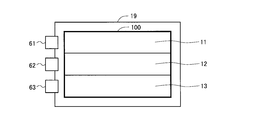
図12は、従来の一般的な液晶表示装置における表示部とゲートドライバとの関係の一例について説明するための図である。図12に示すように、従来の一般的な液晶表示装置においては、矩形の液晶パネル19内に矩形の表示部100が設けられている。図12に示す例では、ゲートドライバは3つのIC(以下、「ゲートドライバIC」という。)61~63によって構成されている。なお、以下においては、このような複数のゲートドライバICを符号によって区別する(ソースドライバICについても同様)。ゲートドライバIC61は、表示部100内の領域のうち符号11を付した領域(以下、便宜上「第1表示領域」という。)に配設されているゲートバスラインを駆動する。ゲートドライバIC62は、表示部100内の領域のうち符号12を付した領域(以下、便宜上「第2表示領域」という。)に配設されているゲートバスラインを駆動する。ゲートドライバIC63は、表示部100内の領域のうち符号13を付した領域(以下、便宜上「第3表示領域」という。)に配設されているゲートバスラインを駆動する。以上のようにして、複数のゲートドライバICが、それぞれ対応する表示領域に配設されているゲートバスラインを駆動している。
なお、ゲートドライバIC61~63の実装方式に関しては、COG(Chip On Glass)方式やCOF(Chip On Film)方式などが採用されている。また、ここでは、ゲートドライバICが用いられている例を挙げて説明したが、モノリシック化されたゲートドライバ(すなわち、液晶パネルを構成するガラス基板上に直接的に形成されたゲートドライバ)が用いられている場合もある。
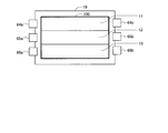
ところで、装置の大型化や高解像度化が進むにつれて、ゲートバスラインを含む回路における時定数が大きくなる。当該時定数が大きくなると、ゲートバスラインによって伝達される走査信号の波形のなまりが大きくなる。そこで、走査信号の波形のなまりが大きくなることを抑制するために、図13に示す構成のようにゲートバスラインを一端型および他端側の双方から駆動するようにした構成もしばしば採用されている。図13に示す例では、ゲートドライバは、第1表示領域11に配設されたゲートバスラインを一端側および他端側からそれぞれ駆動するゲートドライバIC64a,64bと、第2表示領域12に配設されたゲートバスラインを一端側および他端側からそれぞれ駆動するゲートドライバIC65a,65bと、第3表示領域13に配設されたゲートバスラインを一端側および他端側からそれぞれ駆動するゲートドライバIC66a,66bとによって構成されている。このような構成により各ゲートバスラインは一端側および他端側の双方から駆動されるので、たとえ回路の時定数が大きくなっても走査信号の波形のなまりが大きくなることが抑制されている。
なお、図12に示す構成のようにゲートバスラインを一端側から駆動する方式のことを「ゲート片側駆動」といい、図13に示す構成のようにゲートバスラインを一端側および他端側の双方から駆動する方式のことを「ゲート両側駆動」という。
ソースバスラインの駆動に関しても、ソースバスラインを一端側から駆動する「ソース片側駆動」が採用される場合とソースバスラインを一端側および他端側の双方から駆動する「ソース両側駆動」が採用される場合とがある。ソース両側駆動は、映像信号の波形のなまりが大きくなることを抑制するために採用される。図14は、ソース片側駆動が採用されている場合における表示部とソースドライバとの関係の一例について説明するための図である。また、図15は、ソース両側駆動が採用されている場合における表示部とソースドライバとの関係の一例について説明するための図である。なお、これらの例においては、符号14を付した領域を「第1表示領域」といい、符号15を付した領域を「第2表示領域」といい、符号15を付した領域を「第3表示領域」という。図14に示す例では、ソースドライバは、第1表示領域14に配設されたソースバスラインを一端側から駆動するソースドライバIC71と、第2表示領域15に配設されたソースバスラインを一端側から駆動するソースドライバIC72と、第3表示領域16に配設されたソースバスラインを一端側から駆動するソースドライバIC73とによって構成されている。図15に示す例では、ソースドライバは、第1表示領域14に配設されたソースバスラインを一端側および他端側からそれぞれ駆動するソースドライバIC74a,74bと、第2表示領域15に配設されたソースバスラインを一端側および他端側からそれぞれ駆動するソースドライバIC75a,75bと、第3表示領域16に配設されたソースバスラインを一端側および他端側からそれぞれ駆動するソースドライバIC76a,76bとによって構成されている。
なお、本件発明に関連して、以下の先行技術文献が知られている。日本の特開平2-216120号公報には、ゲート片側駆動かつソース片側駆動を採用した構成、ゲート両側駆動かつソース片側駆動を採用した構成、ゲート片側駆動かつソース両側駆動を採用した構成、およびゲート両側駆動かつソース両側駆動を採用した構成が開示されている。
近年、時計用途の液晶表示装置や車載用途の液晶表示装置など、矩形以外の形状の表示部を備えた液晶表示装置の開発が進められている。このような表示装置は「異型ディスプレイ」と呼ばれている。異型ディスプレイにおいては、場所によってゲートバスラインの長さが異なる。そこで、ゲート片側駆動またはゲート両側駆動のいずれを採用するかについては、例えば、最長のゲートバスラインが配設されている領域での時定数の大きさを考慮して決定されている。なお、時定数の大きさは、ゲートバスラインの長さや解像度に依存する。同様に、ソース片側駆動またはソース両側駆動のいずれを採用するかについても、例えば、最長のソースバスラインが配設されている領域での時定数の大きさを考慮して決定されている。
図16は、円形の表示部を有する従来の異型ディスプレイでゲート両側駆動が採用されている場合における表示部とゲートドライバとの関係の一例について説明するための図である。また、図17は、円形の表示部を有する従来の異型ディスプレイでソース両側駆動が採用されている場合における表示部とソースドライバとの関係の一例について説明するための図である。図16に示す例では、ゲートドライバは、第1表示領域11に配設されたゲートバスラインを一端側および他端側からそれぞれ駆動するゲートドライバIC81a,81bと、第2表示領域12に配設されたゲートバスラインを一端側および他端側からそれぞれ駆動するゲートドライバIC82a,82bと、第3表示領域13に配設されたゲートバスラインを一端側および他端側からそれぞれ駆動するゲートドライバIC83a,83bとによって構成されている。図17に示す例では、ソースドライバは、第1表示領域14に配設されたソースバスラインを一端側および他端側からそれぞれ駆動するソースドライバIC91a,91bと、第2表示領域15に配設されたソースバスラインを一端側および他端側からそれぞれ駆動するソースドライバIC92a,92bと、第3表示領域16に配設されたソースバスラインを一端側および他端側からそれぞれ駆動するソースドライバIC93a,93bとによって構成されている。以上のような構成により、異型ディスプレイにおいて、駆動信号(ゲートバスラインによって伝達される走査信号、ソースバスラインによって伝達される走査信号)の波形のなまりが大きくなることが抑制されている。
ところが、両側駆動(ゲート両側駆動、ソース両側駆動)を採用した場合、片側駆動(ゲート片側駆動、ソース片側駆動)が採用した場合と比較して、ドライバの数(例えばICの数)が増えるためコストが高くなる。一方、液晶表示装置等の表示装置に関して、低価格化が強く求められている。
そこで以下の開示は、異型ディスプレイに関し、駆動信号の波形のなまりが大きくなることを抑制しつつ低コスト化を実現することを目的とする。
いくつかの実施形態による表示装置は、信号線として複数の走査信号線および複数の映像信号線が配設された非矩形の表示部と、複数の走査信号線を駆動する走査信号線駆動回路と、複数の映像信号線を駆動する映像信号線駆動回路とを備え、走査信号線駆動回路または映像信号線駆動回路の少なくとも一方は、信号線を一端側のみから駆動する回路部分である第1タイプの駆動回路部と、信号線を一端側および他端側の双方から駆動する一対の回路部分である第2タイプの駆動回路部とからなる。
走査信号線駆動回路または映像信号線駆動回路の少なくとも一方は、信号線を一端側のみから駆動する回路部分である第1タイプの駆動回路部と、信号線を一端側および他端側の双方から駆動する一対の回路部分である第2タイプの駆動回路部とによって構成される。このため、走査信号線あるいは映像信号線あるいはその双方に関して全てを一端側および他端側の双方から駆動する構成と比較して、必要となるドライバの数が少なくなる。これにより、コストが低減される。また、表示部の形状が非矩形であるため場所によって信号線の長さが異なるところ、比較的長い信号線を第2タイプの駆動回路部で駆動することにより駆動信号の波形のなまりが大きくなることが抑制される。以上より、異型ディスプレイに関し、駆動信号の波形のなまりが大きくなることを抑制しつつ低コスト化が実現される。
以下、添付図面を参照しつつ、実施形態について説明する。
<1.第1の実施形態>
<1.1 機能構成および動作概要>
図2は、第1の実施形態に係る液晶表示装置の機能構成を示すブロック図である。なお、図2は機能構成を示す図であるので、各構成要素の形状や構成要素間の位置関係などについては実際とは異なっている。図2に示すように、この液晶表示装置は、表示部100と表示制御回路200とゲートドライバ300とソースドライバ400とを備えている。
<1.1 機能構成および動作概要>
図2は、第1の実施形態に係る液晶表示装置の機能構成を示すブロック図である。なお、図2は機能構成を示す図であるので、各構成要素の形状や構成要素間の位置関係などについては実際とは異なっている。図2に示すように、この液晶表示装置は、表示部100と表示制御回路200とゲートドライバ300とソースドライバ400とを備えている。
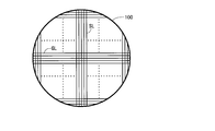
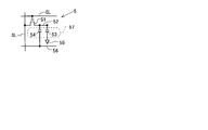
本実施形態においては、表示部100は図3に示すように円形の形状を有している。その表示部100には、複数本のゲートバスライン(走査信号線)GLと複数本のソースバスライン(映像信号線)SLとが配設されている。ゲートバスラインGLとソースバスラインSLとの交差点の近傍には、画素を形成する画素形成部が設けられている。図4は、画素形成部5の構成を示す回路図である。画素形成部5には、対応する交差点を通過するゲートバスラインGLにゲート電極が接続されると共に当該交差点を通過するソースバスラインSLにソース電極が接続されたTFT(薄膜トランジスタ)51と、そのTFT51のドレイン電極に接続された画素電極52と、表示部100内の複数個の画素形成部5に共通的に設けられた共通電極55および補助容量電極56と、画素電極52と共通電極55とによって形成される液晶容量53と、画素電極52と補助容量電極56とによって形成される補助容量54とが含まれている。液晶容量53と補助容量54とによって画素容量57が構成されている。なお、画素形成部5の構成は図4に示す構成には限定されない。例えば、補助容量54および補助容量電極56が設けられていない構成を採用することもできる。
表示部100内のTFT51の種類については特に限定されない。例えば、アモルファスシリコンTFT、LTPS(Low Temperature Poly Silicon)-TFT、酸化物TFT(酸化物半導体をチャネル層に用いたTFT)などを表示部100内のTFT51として採用することができる。酸化物TFTとしては、例えば、インジウム(In),ガリウム(Ga),亜鉛(Zn),および酸素(O)を主成分とする酸化物半導体であるIn-Ga-Zn-O(酸化インジウムガリウム亜鉛)によりチャネル層が形成されたTFTを採用することができる。
次に、図2に示す構成要素の動作について説明する。表示制御回路200は、外部から送られる画像信号DATと水平同期信号や垂直同期信号などのタイミング信号群TGとを受け取り、デジタル映像信号DVと、ゲートドライバ300の動作を制御するためのゲートスタートパルス信号GSPおよびゲートクロック信号GCKと、ソースドライバ400の動作を制御するためのソーススタートパルス信号SSP,ソースクロック信号SCK,およびラッチストローブ信号LSとを出力する。
ゲートドライバ300は、表示制御回路200から送られるゲートスタートパルス信号GSPとゲートクロック信号GCKとに基づいて、アクティブな走査信号の各ゲートバスラインGLへの印加を1垂直走査期間を周期として繰り返す。
ソースドライバ400は、表示制御回路200から送られるデジタル映像信号DV,ソーススタートパルス信号SSP,ソースクロック信号SCK,およびラッチストローブ信号LSを受け取り、ソースバスラインSLに駆動用の映像信号を印加する。このとき、ソースドライバ400では、ソースクロック信号SCKのパルスが発生するタイミングで、各ソースバスラインSLに印加すべき電圧を示すデジタル映像信号DVが順次に保持される。そして、ラッチストローブ信号LSのパルスが発生するタイミングで、上記保持されたデジタル映像信号DVがアナログ電圧に変換される。その変換されたアナログ電圧は、駆動用の映像信号として全てのソースバスラインSLに一斉に印加される。
以上のようにして、ゲートバスラインGLに走査信号が印加され、ソースバスラインSLに駆動用の映像信号が印加されることにより、外部から送られる画像信号DATに応じた画像が表示部100に表示される。
<1.2 表示部とゲートドライバとの関係>
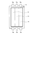
次に、図1を参照しつつ、表示部100とゲートドライバ300との関係について説明する。表示部100内の領域は、図1に示すように、論理的に3つの領域(第1表示領域11~第3表示領域13)に分割されている。換言すれば、表示部100内の領域は、ゲートバスラインGLが伸びる方向とは垂直方向に、表示部100の中心を含む中央領域(第2表示領域12)と該中央領域を挟む2つの周辺領域(第1表示領域11および第3表示領域13)とに論理的に区分されている。ゲートドライバ300は、4つのゲートドライバIC31,32a,32b,および33によって構成されている。これら4つのゲートドライバIC31,32a,32b,および33の実装方式に関しては、COG方式やCOF方式などが採用されている。
次に、図1を参照しつつ、表示部100とゲートドライバ300との関係について説明する。表示部100内の領域は、図1に示すように、論理的に3つの領域(第1表示領域11~第3表示領域13)に分割されている。換言すれば、表示部100内の領域は、ゲートバスラインGLが伸びる方向とは垂直方向に、表示部100の中心を含む中央領域(第2表示領域12)と該中央領域を挟む2つの周辺領域(第1表示領域11および第3表示領域13)とに論理的に区分されている。ゲートドライバ300は、4つのゲートドライバIC31,32a,32b,および33によって構成されている。これら4つのゲートドライバIC31,32a,32b,および33の実装方式に関しては、COG方式やCOF方式などが採用されている。
以上のような構成において、ゲートドライバIC31は第1表示領域11に配設されているゲートバスラインGLを駆動し、ゲートドライバIC32aおよびゲートドライバIC32bは第2表示領域12に配設されているゲートバスラインGLを駆動し、ゲートドライバIC33は第3表示領域13に配設されているゲートバスラインGLを駆動する。すなわち、第1表示領域11(周辺領域)に配設されているゲートバスラインGLについてはゲートドライバIC31によって一端側から駆動され、第2表示領域12(中央領域)に配設されているゲートバスラインGLについてはゲートドライバIC32aおよびゲートドライバIC32bによって一端側および他端側の双方から駆動され、第3表示領域13(周辺領域)に配設されているゲートバスラインGLについてはゲートドライバIC33によって一端側から駆動される。
ここで、信号線を一端側のみから駆動する回路部分を「第1タイプの駆動回路部」と定義し、信号線を一端側および他端側の双方から駆動する一対の回路部分を「第2タイプの駆動回路部」と定義する。そうすると、ゲートドライバIC31とゲートドライバIC33とは、第1タイプの駆動回路部である。また、ゲートドライバIC32aとゲートドライバIC32bとで1つの第2タイプの駆動回路部が構成されている。このように、本実施形態においては、ゲートドライバ300は第1タイプの駆動回路部と第2タイプの駆動回路部とによって構成されている。
ところで、ゲートバスラインGLを含む回路の時定数は、上述したように、ゲートバスラインGLの長さに依存する。また、時定数が大きいほど、走査信号の波形のなまりも大きくなる。従って、ゲートバスラインGLの長さが長いほど、当該ゲートバスラインGLによって伝達される走査信号の波形のなまりが大きくなる。ここで、走査信号の立ち上がりに着目すると、仮に全てのゲートバスラインGLを上述した第1タイプの駆動回路部によって駆動した場合、第1表示領域11あるいは第3表示領域13に配設されている或るゲートバスラインGLでは走査信号の波形は図5で符号6を付した部分のようになまるのに対して、第2表示領域12に配設されている或るゲートバスラインGLでは走査信号の波形は図5で符号7を付した部分のようになまる。すなわち、第2表示領域12では第1表示領域11および第3表示領域13よりも走査信号の波形が大きくなまる。
そこで、本実施形態においては、上述したように、第2表示領域12(中央領域)に配設されているゲートバスラインGLは第2タイプの駆動回路部(すなわち、ゲートドライバIC32aとゲートドライバIC32bとからなる一対の回路部分)によって駆動される構成が採用されている。より詳しくは、各ゲートバスラインGLを第1タイプの駆動回路部または第2タイプの駆動回路部のいずれによって駆動するか(すなわち、各ゲートバスラインGLに関してゲート片側駆動またはゲート両側駆動のいずれを採用するか)が次のように定められ、それに応じて表示部100内の領域が論理的に3つの領域(第1表示領域11~第3表示領域13)に区分されている。時定数の値が所定の基準値よりも小さくなる領域に配設されているゲートバスラインGLについては第1タイプの駆動回路部によって駆動し、時定数の値が当該基準値よりも大きくなる領域に配設されているゲートバスラインGLについては第2タイプの駆動回路部によって駆動する。なお、これについては、次のように定めるようにしても良い。所定の基準長よりも短いゲートバスラインGLについては第1タイプの駆動回路部によって駆動し、当該基準長よりも長いゲートバスラインGLについては第2タイプの駆動回路部によって駆動する。
<1.3 効果>
本実施形態によれば、ゲートドライバ300は、ゲートバスラインGLを一端側のみから駆動する回路部分である第1タイプの駆動回路部と、ゲートバスラインGLを一端側および他端側の双方から駆動する一対の回路部分である第2タイプの駆動回路部とによって構成される。すなわち、一部のゲートバスラインGLについてはゲート両側駆動が行われるが、残りのゲートバスラインGLについてはゲート片側駆動が行われる。このため、全てのゲートバスラインGLに対してゲート両側駆動を行う構成と比較して、ドライバの出力本数を削減することが可能となり、必要となるドライバの数(ゲートドライバICの数)が少なくなるので、コストが低減される。また、表示部100の形状として円形が採用されているところ、比較的長いゲートバスラインGLが配設されている領域(第2表示領域12)ではゲート両側駆動が行われるので、走査信号の波形のなまりが大きくなることが抑制される。以上より、本実施形態によれば、異型ディスプレイに関し、走査信号の波形のなまりが大きくなることを抑制しつつ低コスト化が実現される。
本実施形態によれば、ゲートドライバ300は、ゲートバスラインGLを一端側のみから駆動する回路部分である第1タイプの駆動回路部と、ゲートバスラインGLを一端側および他端側の双方から駆動する一対の回路部分である第2タイプの駆動回路部とによって構成される。すなわち、一部のゲートバスラインGLについてはゲート両側駆動が行われるが、残りのゲートバスラインGLについてはゲート片側駆動が行われる。このため、全てのゲートバスラインGLに対してゲート両側駆動を行う構成と比較して、ドライバの出力本数を削減することが可能となり、必要となるドライバの数(ゲートドライバICの数)が少なくなるので、コストが低減される。また、表示部100の形状として円形が採用されているところ、比較的長いゲートバスラインGLが配設されている領域(第2表示領域12)ではゲート両側駆動が行われるので、走査信号の波形のなまりが大きくなることが抑制される。以上より、本実施形態によれば、異型ディスプレイに関し、走査信号の波形のなまりが大きくなることを抑制しつつ低コスト化が実現される。
<2.第2の実施形態>
<2.1 概要>
上記第1の実施形態においては、ゲートドライバ300が第1タイプの駆動回路部と第2タイプの駆動回路部とによって構成されていた。これに対して、本実施形態においては、ソースドライバ400が第1タイプの駆動回路部と第2タイプの駆動回路部とによって構成される。なお、機能構成および動作概要については、上記第1の実施形態と同様であるので、説明を省略する。
<2.1 概要>
上記第1の実施形態においては、ゲートドライバ300が第1タイプの駆動回路部と第2タイプの駆動回路部とによって構成されていた。これに対して、本実施形態においては、ソースドライバ400が第1タイプの駆動回路部と第2タイプの駆動回路部とによって構成される。なお、機能構成および動作概要については、上記第1の実施形態と同様であるので、説明を省略する。
<2.2 表示部とソースドライバとの関係>
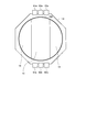
図6を参照しつつ、本実施形態における表示部100とソースドライバ400との関係について説明する。表示部100内の領域は、図6に示すように、論理的に3つの領域(第1表示領域14~第3表示領域16)に分割されている。換言すれば、表示部100内の領域は、ソースバスラインSLが伸びる方向とは垂直方向に、表示部100の中心を含む中央領域(第2表示領域15)と該中央領域を挟む2つの周辺領域(第1表示領域14および第3表示領域16)とに論理的に区分されている。ソースドライバ400は、4つのソースドライバIC41,42a,42b,および43によって構成されている。これら4つのソースドライバIC41,42a,42b,および43の実装方式に関しては、COG方式やCOF方式などが採用されている。
図6を参照しつつ、本実施形態における表示部100とソースドライバ400との関係について説明する。表示部100内の領域は、図6に示すように、論理的に3つの領域(第1表示領域14~第3表示領域16)に分割されている。換言すれば、表示部100内の領域は、ソースバスラインSLが伸びる方向とは垂直方向に、表示部100の中心を含む中央領域(第2表示領域15)と該中央領域を挟む2つの周辺領域(第1表示領域14および第3表示領域16)とに論理的に区分されている。ソースドライバ400は、4つのソースドライバIC41,42a,42b,および43によって構成されている。これら4つのソースドライバIC41,42a,42b,および43の実装方式に関しては、COG方式やCOF方式などが採用されている。
以上のような構成において、ソースドライバIC41は第1表示領域14に配設されているソースバスラインSLを駆動し、ソースドライバIC42aおよびソースドライバIC42bは第2表示領域15に配設されているソースバスラインSLを駆動し、ソースドライバIC43は第3表示領域16に配設されているソースバスラインSLを駆動する。すなわち、第1表示領域14(周辺領域)に配設されているソースバスラインSLについてはソースドライバIC41によって一端側から駆動され、第2表示領域15(中央領域)に配設されているソースバスラインSLについてはソースドライバIC42aおよびソースドライバIC42bによって一端側および他端側の双方から駆動され、第3表示領域16(周辺領域)に配設されているソースバスラインSLについてはソースドライバIC43によって一端側から駆動される。
以上から把握されるように、ソースドライバIC41とソースドライバIC43とは、第1タイプの駆動回路部である。また、ソースドライバIC42aとソースドライバIC42bとで1つの第2タイプの駆動回路部が構成されている。
なお、各ソースバスラインSLを第1タイプの駆動回路部または第2タイプの駆動回路部のいずれによって駆動するかについては、上記第1の実施形態と同様、例えば、各ソースバスラインSLが配設されている領域における時定数の値を所定の基準値と比較することによって決定するようにしても良いし、各ソースバスラインSLの長さを所定の基準長と比較することによって決定するようにしても良い。
<2.3 効果>
本実施形態によれば、ソースドライバ400は、ソースバスラインSLを一端側のみから駆動する回路部分である第1タイプの駆動回路部と、ソースバスラインSLを一端側および他端側の双方から駆動する一対の回路部分である第2タイプの駆動回路部とによって構成される。すなわち、一部のソースバスラインSLについてはソース両側駆動が行われるが、残りのソースバスラインSLについてはソース片側駆動が行われる。このため、全てのソースバスラインSLに対してソース両側駆動を行う構成と比較して、必要となるドライバの数(ソースドライバICの数)が少なくなるので、コストが低減される。また、表示部100の形状として円形が採用されているところ、比較的長いソースバスラインSLが配設されている領域(第2表示領域15)ではソース両側駆動が行われるので、映像信号の波形のなまりが大きくなることが抑制される。以上より、本実施形態によれば、異型ディスプレイに関し、映像信号の波形のなまりが大きくなることを抑制しつつ低コスト化が実現される。
本実施形態によれば、ソースドライバ400は、ソースバスラインSLを一端側のみから駆動する回路部分である第1タイプの駆動回路部と、ソースバスラインSLを一端側および他端側の双方から駆動する一対の回路部分である第2タイプの駆動回路部とによって構成される。すなわち、一部のソースバスラインSLについてはソース両側駆動が行われるが、残りのソースバスラインSLについてはソース片側駆動が行われる。このため、全てのソースバスラインSLに対してソース両側駆動を行う構成と比較して、必要となるドライバの数(ソースドライバICの数)が少なくなるので、コストが低減される。また、表示部100の形状として円形が採用されているところ、比較的長いソースバスラインSLが配設されている領域(第2表示領域15)ではソース両側駆動が行われるので、映像信号の波形のなまりが大きくなることが抑制される。以上より、本実施形態によれば、異型ディスプレイに関し、映像信号の波形のなまりが大きくなることを抑制しつつ低コスト化が実現される。
<3.変形例>
<3.1 第1の変形例>
図7は、上記各実施形態の変形例における表示部100とゲートドライバ300・ソースドライバ400との関係について説明するための図である。図1,図6,および図7から把握されるように、本変形例における構成は、上記第1の実施形態における構成と上記第2の実施形態における構成とを組み合わせた構成となっている。すなわち、ゲートドライバ300およびソースドライバ400の双方が、第1タイプの駆動回路部と第2タイプの駆動回路部とによって構成されている。このような構成を採用することにより、異型ディスプレイに関し、走査信号および映像信号の波形のなまりが大きくなることを抑制しつつ低コスト化が実現される。
<3.1 第1の変形例>
図7は、上記各実施形態の変形例における表示部100とゲートドライバ300・ソースドライバ400との関係について説明するための図である。図1,図6,および図7から把握されるように、本変形例における構成は、上記第1の実施形態における構成と上記第2の実施形態における構成とを組み合わせた構成となっている。すなわち、ゲートドライバ300およびソースドライバ400の双方が、第1タイプの駆動回路部と第2タイプの駆動回路部とによって構成されている。このような構成を採用することにより、異型ディスプレイに関し、走査信号および映像信号の波形のなまりが大きくなることを抑制しつつ低コスト化が実現される。
<3.2 第2の変形例>
上記第1の実施形態においては、第1表示領域11に配設されているゲートバスラインGLを駆動するゲートドライバIC31と第3表示領域13に配設されているゲートバスラインGLを駆動するゲートドライバIC33とが同じ側に配置されていたが、図8に示すように、第1表示領域11に配設されているゲートバスラインGLを駆動するゲートドライバIC34と第3表示領域13に配設されているゲートバスラインGLを駆動するゲートドライバIC36とが異なる側に配置される構成(本変形例の構成)を採用することもできる。なお、本変形例では、第2表示領域12に配設されているゲートバスラインGLについてはゲートドライバIC35a,35bによって一端側および他端側の双方から駆動される。ソースドライバ400についても同様の構成を採用することができる。
上記第1の実施形態においては、第1表示領域11に配設されているゲートバスラインGLを駆動するゲートドライバIC31と第3表示領域13に配設されているゲートバスラインGLを駆動するゲートドライバIC33とが同じ側に配置されていたが、図8に示すように、第1表示領域11に配設されているゲートバスラインGLを駆動するゲートドライバIC34と第3表示領域13に配設されているゲートバスラインGLを駆動するゲートドライバIC36とが異なる側に配置される構成(本変形例の構成)を採用することもできる。なお、本変形例では、第2表示領域12に配設されているゲートバスラインGLについてはゲートドライバIC35a,35bによって一端側および他端側の双方から駆動される。ソースドライバ400についても同様の構成を採用することができる。
<3.3 第3の変形例>
図8に示したような構成(第2の変形例の構成)に関連して、或るゲートドライバICによって駆動される複数本のゲートバスラインGLがゲート片側駆動が行われる領域内のゲートバスラインGLとゲート両側駆動が行われる領域内のゲートバスラインGLとを含むような構成(本変形例の構成)を採用しても良い。これについて、図9を参照しつつ説明する。なお、ゲートバスラインGLの総数は1000本であって各ゲートドライバICの出力本数は400本であると仮定する。このとき、符号K(34)を付した矢印の領域に配設されている400本のゲートバスラインGLをゲートドライバIC34によって駆動させ、符号K(35a)を付した矢印の領域に配設されている400本のゲートバスラインGLをゲートドライバIC35aによって駆動させ、符号K(35b)を付した矢印の領域に配設されている400本のゲートバスラインGLをゲートドライバIC35bによって駆動させ、符号K(36)を付した矢印の領域に配設されている400本のゲートバスラインGLをゲートドライバIC36によって駆動させる。これにより、例えば、上から100本目のゲートバスラインGLについてはゲートドライバIC34によって一端側から駆動され、上から300本目のゲートバスラインGLについてはゲートドライバIC34およびゲートドライバIC35bによって一端側および他端側の双方から駆動され、上から500本目のゲートバスラインGLについてはゲートドライバIC35aおよびゲートドライバIC35bによって一端側および他端側の双方から駆動され、上から700本目のゲートバスラインGLについてはゲートドライバIC35aおよびゲートドライバIC36によって一端側および他端側の双方から駆動され、上から900本目のゲートバスラインGLについてはゲートドライバIC36によって一端側から駆動される。このようにして、第1表示領域11に配設されているゲートバスラインGLおよび第3表示領域13に配設されているゲートバスラインGLについては一端側から駆動され、第2表示領域12に配設されているゲートバスラインGLについては一端側および他端側の双方から駆動される。この構成では、ゲートドライバIC34の一部とゲートドライバIC35aとゲートドライバIC35bとゲートドライバIC36の一部とは、第2タイプの駆動回路部を構成し、ゲートドライバIC34の残りの部分とゲートドライバIC36の残りの部分とは、第1タイプの駆動回路部を構成している。このような構成によれば、ゲート片側駆動とゲート両側駆動との場合分けをゲートドライバIC毎に行う必要がなくなり、設計の自由度が高められる。ソースドライバ400についても同様の構成を採用することができる。
図8に示したような構成(第2の変形例の構成)に関連して、或るゲートドライバICによって駆動される複数本のゲートバスラインGLがゲート片側駆動が行われる領域内のゲートバスラインGLとゲート両側駆動が行われる領域内のゲートバスラインGLとを含むような構成(本変形例の構成)を採用しても良い。これについて、図9を参照しつつ説明する。なお、ゲートバスラインGLの総数は1000本であって各ゲートドライバICの出力本数は400本であると仮定する。このとき、符号K(34)を付した矢印の領域に配設されている400本のゲートバスラインGLをゲートドライバIC34によって駆動させ、符号K(35a)を付した矢印の領域に配設されている400本のゲートバスラインGLをゲートドライバIC35aによって駆動させ、符号K(35b)を付した矢印の領域に配設されている400本のゲートバスラインGLをゲートドライバIC35bによって駆動させ、符号K(36)を付した矢印の領域に配設されている400本のゲートバスラインGLをゲートドライバIC36によって駆動させる。これにより、例えば、上から100本目のゲートバスラインGLについてはゲートドライバIC34によって一端側から駆動され、上から300本目のゲートバスラインGLについてはゲートドライバIC34およびゲートドライバIC35bによって一端側および他端側の双方から駆動され、上から500本目のゲートバスラインGLについてはゲートドライバIC35aおよびゲートドライバIC35bによって一端側および他端側の双方から駆動され、上から700本目のゲートバスラインGLについてはゲートドライバIC35aおよびゲートドライバIC36によって一端側および他端側の双方から駆動され、上から900本目のゲートバスラインGLについてはゲートドライバIC36によって一端側から駆動される。このようにして、第1表示領域11に配設されているゲートバスラインGLおよび第3表示領域13に配設されているゲートバスラインGLについては一端側から駆動され、第2表示領域12に配設されているゲートバスラインGLについては一端側および他端側の双方から駆動される。この構成では、ゲートドライバIC34の一部とゲートドライバIC35aとゲートドライバIC35bとゲートドライバIC36の一部とは、第2タイプの駆動回路部を構成し、ゲートドライバIC34の残りの部分とゲートドライバIC36の残りの部分とは、第1タイプの駆動回路部を構成している。このような構成によれば、ゲート片側駆動とゲート両側駆動との場合分けをゲートドライバIC毎に行う必要がなくなり、設計の自由度が高められる。ソースドライバ400についても同様の構成を採用することができる。
なお、本変形例では、ゲートドライバIC34によって第1駆動ユニットが実現され、ゲートドライバIC35aによって第2駆動ユニットが実現され、ゲートドライバIC35bによって第3駆動ユニットが実現され、ゲートドライバIC36によって第4駆動ユニットが実現されている。
<3.4 第4の変形例>
図10に示すように、図8に示すゲートドライバIC34,35aを1つにまとめたゲートドライバIC37をゲートバスラインGLの一端側に設けるとともに図8に示すゲートドライバIC35b,36を1つにまとめたゲートドライバIC38をゲートバスラインGLの他端側に設ける構成(本変形例の構成)を採用することもできる。この構成について、図11を参照しつつ説明する。なお、ゲートバスラインGLの総数は1000本であって各ゲートドライバICの出力本数は800本であると仮定する。このとき、符号K(37)を付した矢印の領域に配設されている800本のゲートバスラインGLをゲートドライバIC37によって駆動させ、符号K(38)を付した矢印の領域に配設されている800本のゲートバスラインGLをゲートドライバIC38によって駆動させる。換言すれば、第1表示領域11に配設されている200本のゲートバスラインGLをゲートドライバIC37によって駆動させ、第2表示領域12に配設されている600本のゲートバスラインGLをゲートドライバIC37によって一端側から駆動させるとともにゲートドライバ38によって他端側から駆動させ、第3表示領域13に配設されている200本のゲートバスラインGLをゲートドライバIC38によって駆動させる。これにより、例えば、上から100本目のゲートバスラインGLについてはゲートドライバIC37によって一端側から駆動され、上から500本目のゲートバスラインGLについてはゲートドライバIC37およびゲートドライバIC38によって一端側および他端側の双方から駆動され、上から900本目のゲートバスラインGLについてはゲートドライバIC38によって一端側から駆動される。このようにして、第1表示領域11に配設されているゲートバスラインGLおよび第3表示領域13に配設されているゲートバスラインGLについては一端側から駆動され、第2表示領域12に配設されているゲートバスラインGLについては一端側および他端側の双方から駆動される。この構成では、ゲートドライバIC37の一部とゲートドライバIC38の一部とは、第2タイプの駆動回路部を構成し、ゲートドライバIC37の残りの部分とゲートドライバIC38の残りの部分とは、第1タイプの駆動回路部を構成している。このような構成によれば、ゲート片側駆動とゲート両側駆動との場合分けをゲートドライバIC毎に行う必要がなくなり、設計の自由度が高められる。ソースドライバ400についても同様の構成を採用することができる。
図10に示すように、図8に示すゲートドライバIC34,35aを1つにまとめたゲートドライバIC37をゲートバスラインGLの一端側に設けるとともに図8に示すゲートドライバIC35b,36を1つにまとめたゲートドライバIC38をゲートバスラインGLの他端側に設ける構成(本変形例の構成)を採用することもできる。この構成について、図11を参照しつつ説明する。なお、ゲートバスラインGLの総数は1000本であって各ゲートドライバICの出力本数は800本であると仮定する。このとき、符号K(37)を付した矢印の領域に配設されている800本のゲートバスラインGLをゲートドライバIC37によって駆動させ、符号K(38)を付した矢印の領域に配設されている800本のゲートバスラインGLをゲートドライバIC38によって駆動させる。換言すれば、第1表示領域11に配設されている200本のゲートバスラインGLをゲートドライバIC37によって駆動させ、第2表示領域12に配設されている600本のゲートバスラインGLをゲートドライバIC37によって一端側から駆動させるとともにゲートドライバ38によって他端側から駆動させ、第3表示領域13に配設されている200本のゲートバスラインGLをゲートドライバIC38によって駆動させる。これにより、例えば、上から100本目のゲートバスラインGLについてはゲートドライバIC37によって一端側から駆動され、上から500本目のゲートバスラインGLについてはゲートドライバIC37およびゲートドライバIC38によって一端側および他端側の双方から駆動され、上から900本目のゲートバスラインGLについてはゲートドライバIC38によって一端側から駆動される。このようにして、第1表示領域11に配設されているゲートバスラインGLおよび第3表示領域13に配設されているゲートバスラインGLについては一端側から駆動され、第2表示領域12に配設されているゲートバスラインGLについては一端側および他端側の双方から駆動される。この構成では、ゲートドライバIC37の一部とゲートドライバIC38の一部とは、第2タイプの駆動回路部を構成し、ゲートドライバIC37の残りの部分とゲートドライバIC38の残りの部分とは、第1タイプの駆動回路部を構成している。このような構成によれば、ゲート片側駆動とゲート両側駆動との場合分けをゲートドライバIC毎に行う必要がなくなり、設計の自由度が高められる。ソースドライバ400についても同様の構成を採用することができる。
なお、本変形例では、ゲートドライバIC37によって第1回路ユニットが実現され、ゲートドライバIC38によって第2回路ユニットが実現されている。
<4.その他>
上記各実施形態においては液晶表示装置を例に挙げて説明したが、液晶表示装置以外の表示装置についても同様の構成を採用することができる。また、上記各実施形態においては表示部100内の領域が倫理的に3つの領域に分割されている例を挙げて説明したが、表示部100内の領域の分割数は3には限定されない。さらに、上記各実施形態においては表示部100の形状が円形である場合を例に挙げて説明したが、表示部100の形状は円形には限定されない。さらにまた、上記各実施形態においては駆動回路としてICが用いられている例を挙げて説明したが、モノリシック化された駆動回路が用いられていても良い。その他、本発明の趣旨を逸脱しない範囲で種々変形して実施することができる。
上記各実施形態においては液晶表示装置を例に挙げて説明したが、液晶表示装置以外の表示装置についても同様の構成を採用することができる。また、上記各実施形態においては表示部100内の領域が倫理的に3つの領域に分割されている例を挙げて説明したが、表示部100内の領域の分割数は3には限定されない。さらに、上記各実施形態においては表示部100の形状が円形である場合を例に挙げて説明したが、表示部100の形状は円形には限定されない。さらにまた、上記各実施形態においては駆動回路としてICが用いられている例を挙げて説明したが、モノリシック化された駆動回路が用いられていても良い。その他、本発明の趣旨を逸脱しない範囲で種々変形して実施することができる。
<5.付記>
異型ディスプレイとして、以下に示すような様々な構成の表示装置が考えられる。
異型ディスプレイとして、以下に示すような様々な構成の表示装置が考えられる。
(付記1)
信号線として複数の走査信号線および複数の映像信号線が配設された非矩形の表示部と、前記複数の走査信号線を駆動する走査信号線駆動回路と、前記複数の映像信号線を駆動する映像信号線駆動回路とを備えた表示装置であって、
前記走査信号線駆動回路または前記映像信号線駆動回路の少なくとも一方は、信号線を一端側のみから駆動する回路部分である第1タイプの駆動回路部と、信号線を一端側および他端側の双方から駆動する一対の回路部分である第2タイプの駆動回路部とからなる。
信号線として複数の走査信号線および複数の映像信号線が配設された非矩形の表示部と、前記複数の走査信号線を駆動する走査信号線駆動回路と、前記複数の映像信号線を駆動する映像信号線駆動回路とを備えた表示装置であって、
前記走査信号線駆動回路または前記映像信号線駆動回路の少なくとも一方は、信号線を一端側のみから駆動する回路部分である第1タイプの駆動回路部と、信号線を一端側および他端側の双方から駆動する一対の回路部分である第2タイプの駆動回路部とからなる。
このような構成によれば、走査信号線駆動回路または映像信号線駆動回路の少なくとも一方は、信号線を一端側のみから駆動する回路部分である第1タイプの駆動回路部と、信号線を一端側および他端側の双方から駆動する一対の回路部分である第2タイプの駆動回路部とによって構成される。このため、走査信号線あるいは映像信号線あるいはその双方に関して全てを一端側および他端側の双方から駆動する構成と比較して、必要となるドライバの数が少なくなる。これにより、コストが低減される。また、表示部の形状が非矩形であるため場所によって信号線の長さが異なるところ、比較的長い信号線を第2タイプの駆動回路部で駆動することにより駆動信号の波形のなまりが大きくなることが抑制される。以上より、異型ディスプレイに関し、駆動信号の波形のなまりが大きくなることを抑制しつつ低コスト化が実現される。
(付記2)
前記第1タイプの駆動回路部と前記第2タイプの駆動回路部とからなる駆動回路によって駆動される信号線に関し、時定数の値が所定の基準値よりも小さくなる領域に配設されている信号線は前記第1タイプの駆動回路部によって駆動され、時定数の値が前記基準値よりも大きくなる領域に配設されている信号線は前記第2タイプの駆動回路部によって駆動される、付記1に記載の表示装置。
前記第1タイプの駆動回路部と前記第2タイプの駆動回路部とからなる駆動回路によって駆動される信号線に関し、時定数の値が所定の基準値よりも小さくなる領域に配設されている信号線は前記第1タイプの駆動回路部によって駆動され、時定数の値が前記基準値よりも大きくなる領域に配設されている信号線は前記第2タイプの駆動回路部によって駆動される、付記1に記載の表示装置。
このような構成によれば、駆動信号の波形になまりが生じやすい領域では信号線に対していわゆる両側駆動が行われ、駆動信号の波形になまりが生じにくい領域では信号線に対していわゆる片側駆動が行われる。このため、異型ディスプレイに関し、より効果的に、駆動信号の波形のなまりが大きくなることを抑制しつつ低コスト化が実現される。
(付記3)
前記第1タイプの駆動回路部と前記第2タイプの駆動回路部とからなる駆動回路によって駆動される信号線に関し、所定の基準長よりも短い信号線は前記第1タイプの駆動回路部によって駆動され、前記基準長よりも長い信号線は前記第2タイプの駆動回路部によって駆動される、付記1に記載の表示装置。
前記第1タイプの駆動回路部と前記第2タイプの駆動回路部とからなる駆動回路によって駆動される信号線に関し、所定の基準長よりも短い信号線は前記第1タイプの駆動回路部によって駆動され、前記基準長よりも長い信号線は前記第2タイプの駆動回路部によって駆動される、付記1に記載の表示装置。
このような構成によれば、付記2に記載の構成と同様、異型ディスプレイに関し、より効果的に、駆動信号の波形のなまりが大きくなることを抑制しつつ低コスト化が実現される。
(付記4)
前記第1タイプの駆動回路部と前記第2タイプの駆動回路部とからなる駆動回路として、信号線の一端側に配置される第1駆動ユニットと信号線の一端側に配置される第2駆動ユニットと信号線の他端側に配置される第3駆動ユニットと信号線の他端側に配置される第4駆動ユニットとが少なくとも設けられ、
前記第1駆動ユニットの一部と前記第2駆動ユニットと前記第3駆動ユニットと前記第4駆動ユニットの一部とは、前記第2タイプの駆動回路部を構成し、
前記第1駆動ユニットのうち前記第2タイプの駆動回路部を構成しない回路部分と前記第4駆動ユニットのうち前記第2タイプの駆動回路部を構成しない回路部分とは、前記第1タイプの駆動回路部を構成し、
前記第1駆動ユニットのうち前記第1タイプの駆動回路部を構成する回路部分と前記第4駆動ユニットのうち前記第1タイプの駆動回路部を構成する回路部分とは異なる信号線を駆動することを特徴とする、付記1に記載の表示装置。
前記第1タイプの駆動回路部と前記第2タイプの駆動回路部とからなる駆動回路として、信号線の一端側に配置される第1駆動ユニットと信号線の一端側に配置される第2駆動ユニットと信号線の他端側に配置される第3駆動ユニットと信号線の他端側に配置される第4駆動ユニットとが少なくとも設けられ、
前記第1駆動ユニットの一部と前記第2駆動ユニットと前記第3駆動ユニットと前記第4駆動ユニットの一部とは、前記第2タイプの駆動回路部を構成し、
前記第1駆動ユニットのうち前記第2タイプの駆動回路部を構成しない回路部分と前記第4駆動ユニットのうち前記第2タイプの駆動回路部を構成しない回路部分とは、前記第1タイプの駆動回路部を構成し、
前記第1駆動ユニットのうち前記第1タイプの駆動回路部を構成する回路部分と前記第4駆動ユニットのうち前記第1タイプの駆動回路部を構成する回路部分とは異なる信号線を駆動することを特徴とする、付記1に記載の表示装置。
このような構成によれば、駆動信号の波形のなまりが大きくなることを抑制することのできる異型ディスプレイを低コストで実現する際に、ゲート片側駆動とゲート両側駆動との場合分けを駆動ユニット毎(例えば、ゲートドライバIC毎、ソースドライバIC毎)に行う必要がなくなり、設計の自由度が高められる。
(付記5)
前記第1タイプの駆動回路部と前記第2タイプの駆動回路部とからなる駆動回路として、信号線の一端側に配置される第1回路ユニットと信号線の他端側に配置される第2回路ユニットとが少なくとも設けられ、
前記第1回路ユニットの一部と前記第2回路ユニットの一部とは、前記第2タイプの駆動回路部を構成し、
前記第1回路ユニットのうち前記第2タイプの駆動回路部を構成しない回路部分と前記第2回路ユニットのうち前記第2タイプの駆動回路部を構成しない回路部分とは、前記第1タイプの駆動回路部を構成し、
前記第1回路ユニットのうち前記第1タイプの駆動回路部を構成する回路部分と前記第2回路ユニットのうち前記第1タイプの駆動回路部を構成する回路部分とは異なる信号線を駆動することを特徴とする、付記1に記載の表示装置。
前記第1タイプの駆動回路部と前記第2タイプの駆動回路部とからなる駆動回路として、信号線の一端側に配置される第1回路ユニットと信号線の他端側に配置される第2回路ユニットとが少なくとも設けられ、
前記第1回路ユニットの一部と前記第2回路ユニットの一部とは、前記第2タイプの駆動回路部を構成し、
前記第1回路ユニットのうち前記第2タイプの駆動回路部を構成しない回路部分と前記第2回路ユニットのうち前記第2タイプの駆動回路部を構成しない回路部分とは、前記第1タイプの駆動回路部を構成し、
前記第1回路ユニットのうち前記第1タイプの駆動回路部を構成する回路部分と前記第2回路ユニットのうち前記第1タイプの駆動回路部を構成する回路部分とは異なる信号線を駆動することを特徴とする、付記1に記載の表示装置。
このような構成によれば、付記4に記載の構成と同様の効果が得られる。
(付記6)
前記表示部の形状は、円形であって、
前記表示部の領域は、前記第1タイプの駆動回路部と前記第2タイプの駆動回路部とからなる駆動回路によって駆動される信号線が伸びる方向とは垂直方向に、前記表示部の中心を含む中央領域と該中央領域を挟む2つの周辺領域とに論理的に区分され、
前記第1タイプの駆動回路部と前記第2タイプの駆動回路部とからなる駆動回路によって駆動される信号線に関し、前記周辺領域に配設されている信号線は前記第1タイプの駆動回路部によって駆動され、前記中央領域に配設されている信号線は前記第2タイプの駆動回路部によって駆動される、付記1に記載の表示装置。
前記表示部の形状は、円形であって、
前記表示部の領域は、前記第1タイプの駆動回路部と前記第2タイプの駆動回路部とからなる駆動回路によって駆動される信号線が伸びる方向とは垂直方向に、前記表示部の中心を含む中央領域と該中央領域を挟む2つの周辺領域とに論理的に区分され、
前記第1タイプの駆動回路部と前記第2タイプの駆動回路部とからなる駆動回路によって駆動される信号線に関し、前記周辺領域に配設されている信号線は前記第1タイプの駆動回路部によって駆動され、前記中央領域に配設されている信号線は前記第2タイプの駆動回路部によって駆動される、付記1に記載の表示装置。
このような構成によれば、付記1に記載の構成と同様の効果が得られる。
(付記7)
前記走査信号線駆動回路が前記第1タイプの駆動回路部と前記第2タイプの駆動回路部とからなる、付記1に記載の表示装置。
前記走査信号線駆動回路が前記第1タイプの駆動回路部と前記第2タイプの駆動回路部とからなる、付記1に記載の表示装置。
このような構成によれば、異型ディスプレイに関し、走査信号の波形のなまりが大きくなることを抑制しつつ低コスト化が実現される。
(付記8)
前記映像信号線駆動回路が前記第1タイプの駆動回路部と前記第2タイプの駆動回路部とからなる、付記1に記載の表示装置。
前記映像信号線駆動回路が前記第1タイプの駆動回路部と前記第2タイプの駆動回路部とからなる、付記1に記載の表示装置。
このような構成によれば、異型ディスプレイに関し、映像信号の波形のなまりが大きくなることを抑制しつつ低コスト化が実現される。
(付記9)
前記走査信号線駆動回路および前記映像信号線駆動回路の双方が前記第1タイプの駆動回路部と前記第2タイプの駆動回路部とからなる、付記1に記載の表示装置。
前記走査信号線駆動回路および前記映像信号線駆動回路の双方が前記第1タイプの駆動回路部と前記第2タイプの駆動回路部とからなる、付記1に記載の表示装置。
このような構成によれば、異型ディスプレイに関し、走査信号および映像信号の波形のなまりが大きくなることを抑制しつつ低コスト化が実現される。
<6.優先権主張に関して>
本願は、2017年4月11日に出願された「表示装置」という名称の日本出願2017-78208号に基づく優先権を主張する出願であり、この日本出願の内容は、引用することによって本願の中に含まれる。
本願は、2017年4月11日に出願された「表示装置」という名称の日本出願2017-78208号に基づく優先権を主張する出願であり、この日本出願の内容は、引用することによって本願の中に含まれる。
19…液晶パネル
31,32a,32b,33,34,35a,35b,36…ゲートドライバIC
41,42a,42b,43,44,45a,45b,46…ソースドライバIC
100…表示部
300…ゲートドライバ
400…ソースドライバ
31,32a,32b,33,34,35a,35b,36…ゲートドライバIC
41,42a,42b,43,44,45a,45b,46…ソースドライバIC
100…表示部
300…ゲートドライバ
400…ソースドライバ
Claims (9)
- 信号線として複数の走査信号線および複数の映像信号線が配設された非矩形の表示部と、前記複数の走査信号線を駆動する走査信号線駆動回路と、前記複数の映像信号線を駆動する映像信号線駆動回路とを備えた表示装置であって、
前記走査信号線駆動回路または前記映像信号線駆動回路の少なくとも一方は、信号線を一端側のみから駆動する回路部分である第1タイプの駆動回路部と、信号線を一端側および他端側の双方から駆動する一対の回路部分である第2タイプの駆動回路部とからなることを特徴とする、表示装置。 - 前記第1タイプの駆動回路部と前記第2タイプの駆動回路部とからなる駆動回路によって駆動される信号線に関し、時定数の値が所定の基準値よりも小さくなる領域に配設されている信号線は前記第1タイプの駆動回路部によって駆動され、時定数の値が前記基準値よりも大きくなる領域に配設されている信号線は前記第2タイプの駆動回路部によって駆動されることを特徴とする、請求項1に記載の表示装置。
- 前記第1タイプの駆動回路部と前記第2タイプの駆動回路部とからなる駆動回路によって駆動される信号線に関し、所定の基準長よりも短い信号線は前記第1タイプの駆動回路部によって駆動され、前記基準長よりも長い信号線は前記第2タイプの駆動回路部によって駆動されることを特徴とする、請求項1に記載の表示装置。
- 前記第1タイプの駆動回路部と前記第2タイプの駆動回路部とからなる駆動回路として、信号線の一端側に配置される第1駆動ユニットと信号線の一端側に配置される第2駆動ユニットと信号線の他端側に配置される第3駆動ユニットと信号線の他端側に配置される第4駆動ユニットとが少なくとも設けられ、
前記第1駆動ユニットの一部と前記第2駆動ユニットと前記第3駆動ユニットと前記第4駆動ユニットの一部とは、前記第2タイプの駆動回路部を構成し、
前記第1駆動ユニットのうち前記第2タイプの駆動回路部を構成しない回路部分と前記第4駆動ユニットのうち前記第2タイプの駆動回路部を構成しない回路部分とは、前記第1タイプの駆動回路部を構成し、
前記第1駆動ユニットのうち前記第1タイプの駆動回路部を構成する回路部分と前記第4駆動ユニットのうち前記第1タイプの駆動回路部を構成する回路部分とは異なる信号線を駆動することを特徴とする、請求項1に記載の表示装置。 - 前記第1タイプの駆動回路部と前記第2タイプの駆動回路部とからなる駆動回路として、信号線の一端側に配置される第1回路ユニットと信号線の他端側に配置される第2回路ユニットとが少なくとも設けられ、
前記第1回路ユニットの一部と前記第2回路ユニットの一部とは、前記第2タイプの駆動回路部を構成し、
前記第1回路ユニットのうち前記第2タイプの駆動回路部を構成しない回路部分と前記第2回路ユニットのうち前記第2タイプの駆動回路部を構成しない回路部分とは、前記第1タイプの駆動回路部を構成し、
前記第1回路ユニットのうち前記第1タイプの駆動回路部を構成する回路部分と前記第2回路ユニットのうち前記第1タイプの駆動回路部を構成する回路部分とは異なる信号線を駆動することを特徴とする、請求項1に記載の表示装置。 - 前記表示部の形状は、円形であって、
前記表示部の領域は、前記第1タイプの駆動回路部と前記第2タイプの駆動回路部とからなる駆動回路によって駆動される信号線が伸びる方向とは垂直方向に、前記表示部の中心を含む中央領域と該中央領域を挟む2つの周辺領域とに論理的に区分され、
前記第1タイプの駆動回路部と前記第2タイプの駆動回路部とからなる駆動回路によって駆動される信号線に関し、前記周辺領域に配設されている信号線は前記第1タイプの駆動回路部によって駆動され、前記中央領域に配設されている信号線は前記第2タイプの駆動回路部によって駆動されることを特徴とする、請求項1に記載の表示装置。 - 前記走査信号線駆動回路が前記第1タイプの駆動回路部と前記第2タイプの駆動回路部とからなることを特徴とする、請求項1に記載の表示装置。
- 前記映像信号線駆動回路が前記第1タイプの駆動回路部と前記第2タイプの駆動回路部とからなることを特徴とする、請求項1に記載の表示装置。
- 前記走査信号線駆動回路および前記映像信号線駆動回路の双方が前記第1タイプの駆動回路部と前記第2タイプの駆動回路部とからなることを特徴とすることを特徴とする、請求項1に記載の表示装置。
Priority Applications (2)
| Application Number | Priority Date | Filing Date | Title |
|---|---|---|---|
| US16/604,175 US10803824B2 (en) | 2017-04-11 | 2018-04-04 | Driving circuit for non-rectangular display unit |
| CN201880024332.XA CN110520924B (zh) | 2017-04-11 | 2018-04-04 | 显示装置 |
Applications Claiming Priority (2)
| Application Number | Priority Date | Filing Date | Title |
|---|---|---|---|
| JP2017078208 | 2017-04-11 | ||
| JP2017-078208 | 2017-04-11 |
Publications (1)
| Publication Number | Publication Date |
|---|---|
| WO2018190206A1 true WO2018190206A1 (ja) | 2018-10-18 |
Family
ID=63792636
Family Applications (1)
| Application Number | Title | Priority Date | Filing Date |
|---|---|---|---|
| PCT/JP2018/014357 Ceased WO2018190206A1 (ja) | 2017-04-11 | 2018-04-04 | 表示装置 |
Country Status (3)
| Country | Link |
|---|---|
| US (1) | US10803824B2 (ja) |
| CN (1) | CN110520924B (ja) |
| WO (1) | WO2018190206A1 (ja) |
Citations (3)
| Publication number | Priority date | Publication date | Assignee | Title |
|---|---|---|---|---|
| KR20110065823A (ko) * | 2009-12-10 | 2011-06-16 | 엘지디스플레이 주식회사 | 액정표시장치 |
| WO2014142183A1 (ja) * | 2013-03-15 | 2014-09-18 | シャープ株式会社 | アクティブマトリクス基板、アクティブマトリクス基板の製造方法、及び表示パネル |
| WO2017221844A1 (ja) * | 2016-06-21 | 2017-12-28 | シャープ株式会社 | 表示パネルおよび表示装置 |
Family Cites Families (14)
| Publication number | Priority date | Publication date | Assignee | Title |
|---|---|---|---|---|
| JPH02216120A (ja) | 1989-02-17 | 1990-08-29 | Seiko Epson Corp | 液晶電気光学素子の駆動方法 |
| JP3744819B2 (ja) * | 2001-05-24 | 2006-02-15 | セイコーエプソン株式会社 | 信号駆動回路、表示装置、電気光学装置及び信号駆動方法 |
| JP4320682B2 (ja) * | 2006-07-20 | 2009-08-26 | セイコーエプソン株式会社 | 表示装置、表示装置の駆動方法及び電子機器 |
| US8023087B2 (en) * | 2006-08-23 | 2011-09-20 | Hitachi Displays, Ltd. | Display device having particular pixels and signal wiring internal circuits |
| KR20090083677A (ko) * | 2008-01-30 | 2009-08-04 | 삼성전자주식회사 | 표시 장치 |
| JP5839896B2 (ja) * | 2010-09-09 | 2016-01-06 | 株式会社半導体エネルギー研究所 | 表示装置 |
| KR20140109261A (ko) * | 2013-03-05 | 2014-09-15 | 가부시키가이샤 한도오따이 에네루기 켄큐쇼 | 표시 장치 및 전자 기기 |
| KR102049736B1 (ko) * | 2013-06-25 | 2019-11-28 | 엘지디스플레이 주식회사 | 타이밍 제어부를 포함하는 디스플레이 장치 |
| CN104361877B (zh) * | 2014-12-09 | 2016-08-17 | 京东方科技集团股份有限公司 | 一种显示面板的驱动方法、其驱动装置及显示装置 |
| KR20160096791A (ko) * | 2015-02-05 | 2016-08-17 | 삼성디스플레이 주식회사 | 비사각형 표시 장치 |
| KR102276995B1 (ko) * | 2015-02-12 | 2021-07-21 | 삼성디스플레이 주식회사 | 비사각형 디스플레이 |
| WO2017119338A1 (ja) * | 2016-01-04 | 2017-07-13 | シャープ株式会社 | 表示装置 |
| US10395599B2 (en) * | 2016-02-29 | 2019-08-27 | Samsung Display Co., Ltd. | Display device |
| CN106448587B (zh) * | 2016-10-08 | 2019-09-20 | 京东方科技集团股份有限公司 | 显示面板及其制造方法、显示装置 |
-
2018
- 2018-04-04 WO PCT/JP2018/014357 patent/WO2018190206A1/ja not_active Ceased
- 2018-04-04 CN CN201880024332.XA patent/CN110520924B/zh active Active
- 2018-04-04 US US16/604,175 patent/US10803824B2/en active Active
Patent Citations (3)
| Publication number | Priority date | Publication date | Assignee | Title |
|---|---|---|---|---|
| KR20110065823A (ko) * | 2009-12-10 | 2011-06-16 | 엘지디스플레이 주식회사 | 액정표시장치 |
| WO2014142183A1 (ja) * | 2013-03-15 | 2014-09-18 | シャープ株式会社 | アクティブマトリクス基板、アクティブマトリクス基板の製造方法、及び表示パネル |
| WO2017221844A1 (ja) * | 2016-06-21 | 2017-12-28 | シャープ株式会社 | 表示パネルおよび表示装置 |
Also Published As
| Publication number | Publication date |
|---|---|
| CN110520924B (zh) | 2021-11-30 |
| CN110520924A (zh) | 2019-11-29 |
| US20200051519A1 (en) | 2020-02-13 |
| US10803824B2 (en) | 2020-10-13 |
Similar Documents
| Publication | Publication Date | Title |
|---|---|---|
| US8471981B2 (en) | Display apparatus and display set having the same | |
| US8860706B2 (en) | Display device | |
| US8462099B2 (en) | Display panel and display device | |
| CN101739935B (zh) | 电光装置及电子设备 | |
| JP2006330682A (ja) | アモルファスシリコンlcdのゲートスイッチ装置 | |
| CN104081445B (zh) | 显示装置及其驱动方法 | |
| WO2011036911A1 (ja) | 液晶表示装置 | |
| US7894030B2 (en) | Liquid crystal display and method havng three pixel electrodes adjacent each other in a column direction connected with three respective gate lines that are commonly connected and three data lines, two of which are overlapped by all three pixel electrodes | |
| KR20060097819A (ko) | 쉬프트 레지스터 및 이를 구비한 표시 장치 | |
| CN104094347B (zh) | 显示装置及其驱动方法 | |
| US10838278B2 (en) | Liquid crystal display device | |
| US20070097052A1 (en) | Liquid crystal display device | |
| KR101730995B1 (ko) | 표시장치 | |
| US9865212B2 (en) | Display device | |
| US20110063260A1 (en) | Driving circuit for liquid crystal display | |
| WO2018190206A1 (ja) | 表示装置 | |
| TWI325131B (en) | Driving circuit of electro-optical device, electro-optical device having driving circuit, and electronic apparatus | |
| JP5909067B2 (ja) | 表示装置 | |
| JPH09236790A (ja) | 液晶表示装置およびその駆動方法 | |
| JP2007279625A (ja) | 電気光学装置及びその駆動方法、並びに電子機器 | |
| JP6452710B2 (ja) | ゲート側ファンアウト区域の回路構造 | |
| JP2012173499A (ja) | 液晶表示装置の駆動装置 | |
| JPH11175041A (ja) | 半導体装置及びその駆動方法 | |
| WO2012073467A1 (ja) | 液晶表示装置 | |
| CN110264974B (zh) | 像素电路及其驱动方法、阵列基板、显示面板、显示装置 |
Legal Events
| Date | Code | Title | Description |
|---|---|---|---|
| 121 | Ep: the epo has been informed by wipo that ep was designated in this application |
Ref document number: 18784335 Country of ref document: EP Kind code of ref document: A1 |
|
| NENP | Non-entry into the national phase |
Ref country code: DE |
|
| 122 | Ep: pct application non-entry in european phase |
Ref document number: 18784335 Country of ref document: EP Kind code of ref document: A1 |
|
| NENP | Non-entry into the national phase |
Ref country code: JP |