WO2018181593A1 - 銅板付き絶縁基板用銅板材及びその製造方法 - Google Patents
銅板付き絶縁基板用銅板材及びその製造方法 Download PDFInfo
- Publication number
- WO2018181593A1 WO2018181593A1 PCT/JP2018/013002 JP2018013002W WO2018181593A1 WO 2018181593 A1 WO2018181593 A1 WO 2018181593A1 JP 2018013002 W JP2018013002 W JP 2018013002W WO 2018181593 A1 WO2018181593 A1 WO 2018181593A1
- Authority
- WO
- WIPO (PCT)
- Prior art keywords
- copper plate
- copper
- heat treatment
- plate material
- insulating substrate
- Prior art date
- Legal status (The legal status is an assumption and is not a legal conclusion. Google has not performed a legal analysis and makes no representation as to the accuracy of the status listed.)
- Ceased
Links
Images
Classifications
-
- C—CHEMISTRY; METALLURGY
- C04—CEMENTS; CONCRETE; ARTIFICIAL STONE; CERAMICS; REFRACTORIES
- C04B—LIME, MAGNESIA; SLAG; CEMENTS; COMPOSITIONS THEREOF, e.g. MORTARS, CONCRETE OR LIKE BUILDING MATERIALS; ARTIFICIAL STONE; CERAMICS; REFRACTORIES; TREATMENT OF NATURAL STONE
- C04B37/00—Joining burned ceramic articles with other burned ceramic articles or other articles by heating
- C04B37/02—Joining burned ceramic articles with other burned ceramic articles or other articles by heating with metallic articles
- C04B37/021—Joining burned ceramic articles with other burned ceramic articles or other articles by heating with metallic articles in a direct manner, e.g. direct copper bonding [DCB]
-
- C—CHEMISTRY; METALLURGY
- C22—METALLURGY; FERROUS OR NON-FERROUS ALLOYS; TREATMENT OF ALLOYS OR NON-FERROUS METALS
- C22C—ALLOYS
- C22C9/00—Alloys based on copper
-
- C—CHEMISTRY; METALLURGY
- C22—METALLURGY; FERROUS OR NON-FERROUS ALLOYS; TREATMENT OF ALLOYS OR NON-FERROUS METALS
- C22C—ALLOYS
- C22C9/00—Alloys based on copper
- C22C9/01—Alloys based on copper with aluminium as the next major constituent
-
- C—CHEMISTRY; METALLURGY
- C22—METALLURGY; FERROUS OR NON-FERROUS ALLOYS; TREATMENT OF ALLOYS OR NON-FERROUS METALS
- C22C—ALLOYS
- C22C9/00—Alloys based on copper
- C22C9/02—Alloys based on copper with tin as the next major constituent
-
- C—CHEMISTRY; METALLURGY
- C22—METALLURGY; FERROUS OR NON-FERROUS ALLOYS; TREATMENT OF ALLOYS OR NON-FERROUS METALS
- C22C—ALLOYS
- C22C9/00—Alloys based on copper
- C22C9/06—Alloys based on copper with nickel or cobalt as the next major constituent
-
- C—CHEMISTRY; METALLURGY
- C22—METALLURGY; FERROUS OR NON-FERROUS ALLOYS; TREATMENT OF ALLOYS OR NON-FERROUS METALS
- C22C—ALLOYS
- C22C9/00—Alloys based on copper
- C22C9/08—Alloys based on copper with lead as the next major constituent
-
- C—CHEMISTRY; METALLURGY
- C22—METALLURGY; FERROUS OR NON-FERROUS ALLOYS; TREATMENT OF ALLOYS OR NON-FERROUS METALS
- C22F—CHANGING THE PHYSICAL STRUCTURE OF NON-FERROUS METALS AND NON-FERROUS ALLOYS
- C22F1/00—Changing the physical structure of non-ferrous metals or alloys by heat treatment or by hot or cold working
- C22F1/08—Changing the physical structure of non-ferrous metals or alloys by heat treatment or by hot or cold working of copper or alloys based thereon
-
- C—CHEMISTRY; METALLURGY
- C04—CEMENTS; CONCRETE; ARTIFICIAL STONE; CERAMICS; REFRACTORIES
- C04B—LIME, MAGNESIA; SLAG; CEMENTS; COMPOSITIONS THEREOF, e.g. MORTARS, CONCRETE OR LIKE BUILDING MATERIALS; ARTIFICIAL STONE; CERAMICS; REFRACTORIES; TREATMENT OF NATURAL STONE
- C04B2237/00—Aspects relating to ceramic laminates or to joining of ceramic articles with other articles by heating
- C04B2237/30—Composition of layers of ceramic laminates or of ceramic or metallic articles to be joined by heating, e.g. Si substrates
- C04B2237/40—Metallic
- C04B2237/407—Copper
-
- C—CHEMISTRY; METALLURGY
- C22—METALLURGY; FERROUS OR NON-FERROUS ALLOYS; TREATMENT OF ALLOYS OR NON-FERROUS METALS
- C22F—CHANGING THE PHYSICAL STRUCTURE OF NON-FERROUS METALS AND NON-FERROUS ALLOYS
- C22F1/00—Changing the physical structure of non-ferrous metals or alloys by heat treatment or by hot or cold working
Definitions
- the present invention relates to a copper plate material for an insulating substrate with a copper plate, particularly a copper plate material suitable for an insulating substrate with a copper plate of a power device, and a method for manufacturing the same.
- a joining method for joining via a silver-based brazing material or a joining method using a eutectic reaction of copper without using a brazing material is used.
- both require heat treatment at a high temperature of 700 ° C. or higher.
- aluminum nitride, alumina, silicon nitride, or the like is used for the ceramic substrate, these thermal expansion coefficients are different from the thermal expansion coefficient of copper constituting the copper plate. For this reason, when the ceramic substrate and the copper plate are bonded at a high temperature, a large strain tends to be generated in the entire insulating substrate due to a difference in thermal expansion coefficient.
- the copper plate material has a higher coefficient of thermal expansion than the ceramic substrate and the copper plate material, when heat treatment is performed, tensile stress is applied to the ceramic substrate and compressive stress is applied to the copper plate material. As a result, not only the entire insulating substrate is deformed and a dimensional change occurs, but peeling or the like between the ceramic substrate and the copper plate material easily occurs. Furthermore, high-purity copper used for a copper plate material grows crystal grains remarkably at a high temperature of 700 ° C. or higher, making it difficult to homogenize the structure. For this reason, there is a problem that the bondability is deteriorated, and when a strain occurs, it becomes a starting point of grain boundary fracture.
- Patent Document 1 discloses a pure copper plate made of pure copper having a purity of 99.90 mass% or more and having a specified X-ray diffraction intensity ratio as a pure copper plate used for a heat dissipation substrate.
- Patent Document 2 discloses a copper alloy plate having a tensile strength of 350 MPa or more and a controlled degree of crystal orientation integration at a predetermined position as a copper alloy plate suitable for a heat dissipation electronic component, a high-current electronic component, and the like. Is disclosed.
- JP 2014-189817 A Japanese Patent No. 5475914
- the pure copper plate disclosed in Patent Document 1 is considered to have excellent adhesion to other members because the surface is not easily roughened by etching, but it is bonded to other members at high temperatures. Has not been studied at all.
- the copper alloy plate currently disclosed by patent document 2 is examined regarding heat resistance, only the heat resistance by heat processing for 30 minutes at 200 degreeC is considered.
- the copper alloy plate disclosed in Patent Document 2 has a tensile strength of 350 MPa or more and does not correspond to a range of 150 to 330 MPa suitable as a copper plate material used for an insulating substrate with a copper plate.
- an object of the present invention is to have a low longitudinal elastic modulus continuously from the rolling direction to the sheet width direction, excellent in tensile strength and conductivity, and heat treatment at a high temperature (for example, 700 ° C. to 800 ° C. for 10 minutes to 5 minutes).
- An object of the present invention is to provide a copper plate material for an insulating substrate with a copper plate in which the growth of crystal grains is suppressed when a heat treatment for less than the time is performed, and a method for producing the same.
- the present inventors control the longitudinal elastic modulus of the copper plate material and suppress the growth of crystal grains at a high temperature of 700 ° C. or higher, so that the copper plate material and the ceramic substrate can be bonded together. It has been found that the load stress of the entire substrate caused by the difference in thermal expansion coefficient can be reduced, and that the heterogeneity of the structure and the deterioration of the bonding property due to the growth of crystal grains can be suppressed.
- the gist configuration of the present invention is as follows. (1) The total content of metal components selected from the group consisting of Al, Be, Cd, Mg, Pb, Ni, P, Sn, and Cr is 0.1 to 2.0 ppm, and the copper content is 99.96 mass.
- the copper content is 99.99 mass% or more, and the average value of the longitudinal elastic modulus is 115 GPa or less, and the longitudinal elastic modulus is the rolling direction, the sheet width direction, and the direction between them.
- the copper plate material for an insulating substrate with a copper plate according to (1) which is measured by: (3) The copper plate material for an insulating substrate with a copper plate according to (1) or (2), wherein the average crystal grain size is 3 ⁇ m to 100 ⁇ m.
- a method for producing a copper plate material for an insulating substrate with a copper plate according to any one of (1) to (5) A homogenization heat treatment step of performing a homogenization heat treatment on the ingot obtained by casting the copper material having the composition; A hot rolling step for performing hot rolling after the homogenizing heat treatment step; A cooling step for cooling after the hot rolling step; A chamfering step for chamfering both surfaces of the rolled material after the cooling step; A first cold rolling step for performing cold rolling with a total processing rate of 75% or more after the chamfering step; After the first cold rolling step, the temperature raising rate is 1 to 100 ° C./second, the attained temperature is 100 to 500 ° C., the holding time is 1 to 900 seconds, and the cooling rate is 1 to 50 ° C./
- a first annealing step in which heat treatment is performed After the first annealing step, a second cold rolling step of performing cold rolling with a total processing rate of 60 to 95%; Conditions after the second cold rolling step that the heating rate is 10 to 100 ° C./second, the ultimate temperature is 200 to 550 ° C., the holding time is 10 to 3600 seconds, and the cooling rate is 10 to 100 ° C./second
- a second annealing step for performing heat treatment at A finish rolling step for further rolling after the second annealing step After the finish rolling step, a final annealing step for applying a final heat treatment, After the final annealing step, a surface oxide film removing step for pickling and polishing,
- the manufacturing method of the copper plate material for insulation boards with a copper plate containing After the first annealing step, a second cold rolling step of performing cold rolling with a total processing rate of 60 to 95%; Conditions after the second cold rolling step that the heating rate is 10 to 100 ° C./second, the ultimate temperature
- the longitudinal elastic modulus is continuously low from the rolling direction to the sheet width direction, the tensile strength and the electrical conductivity are excellent, and the heat treatment is performed at a high temperature (for example, 700 ° C. to 800 ° C. for 10 minutes to 5 hours). It is possible to provide a copper plate material for an insulating substrate with a copper plate that suppresses the growth of crystal grains when the heat treatment is performed, and a method for producing the same.
- the numerical range expressed using “to” means a range including numerical values described before and after “to” as the lower limit value and the upper limit value.
- the copper plate material of the present invention has a total content of metal components selected from the group consisting of Al, Be, Cd, Mg, Pb, Ni, P, Sn and Cr of 0.1 to 2.0 ppm, and a copper content
- ⁇ 2 0 °
- the copper material means that a copper material (before processing and having a predetermined composition) is processed into a predetermined shape (for example, a plate, a strip, a foil, a bar, a wire, etc.).
- a predetermined shape for example, a plate, a strip, a foil, a bar, a wire, etc.
- the “plate material” refers to a material having a specific thickness, having a stable shape and having a spread in the surface direction, and includes a strip material in a broad sense.
- the thickness of the copper plate material is not particularly limited, but is preferably 0.05 to 7.0 mm, more preferably 0.1 to 6.0 mm.
- the copper content is 99.96 mass% or more, preferably 99.99 mass% or more. If the copper content is less than 99.96 mass%, the thermal conductivity is lowered and the desired heat dissipation cannot be obtained.
- the total content of metal components selected from the group consisting of Al, Be, Cd, Mg, Pb, Ni, P, Sn, and Cr is 0.1 to 2.0 ppm, and 0.1 to 1.0 ppm. It is preferable that The lower limit of the total content of these metal components is not particularly limited, but is 0.1 ppm in consideration of inevitable impurities. On the other hand, when the total content of these metal components exceeds 2.0 ppm, a desired orientation density cannot be obtained.
- the copper plate material contains inevitable impurities as the balance. Also good. Inevitable impurities mean impurities at a content level that can be inevitably included in the manufacturing process.
- the GDMS method can be used for quantitative analysis of the above metal components other than copper.
- the GDMS method is an abbreviation of Glow Discharge Mass Spectrometry. Specifically, a solid sample is used as a cathode, the sample surface is sputtered using glow discharge, and the emitted neutral particles collide with Ar or electrons in the plasma. This is a technique for analyzing the proportion of trace elements contained in a metal by measuring the number of ions with a mass analyzer.
- the copper plate material of the present invention has a rolling texture, and this rolling texture is obtained by converting a crystal orientation distribution function (ODF) obtained from texture analysis by EBSD to Euler angles ( ⁇ 1, ⁇ , ⁇ 2). ),
- ODF crystal orientation distribution function
- Rotation direction with RD direction as axis when rolling direction is RD direction sheet width direction (direction perpendicular to RD direction) is TD direction, and direction perpendicular to rolling surface (RD surface) is ND direction Is represented as ⁇ 1 and azimuth rotation about the TD direction is represented as ⁇ 2.
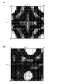
- the orientation density is a parameter used when quantitatively analyzing the abundance ratio and dispersion state of crystal orientation in the texture. EBSD and X-ray diffraction are performed, and (100), (110), (112), etc. It is calculated by a crystal orientation distribution analysis method by a series expansion method based on the measurement data of three or more types of positive point maps. In a cross-sectional view obtained by texture analysis by EBSD and fixing ⁇ 2 at a predetermined angle, the distribution of orientation density in the RD plane is shown.
- FIGS. 1A and 1 (B) are diagrams showing the results of analyzing the rolling texture of the copper sheet material of the present invention by EBSD.
- the crystal orientation distribution is random, it is assumed that the orientation density is 1, and the number of times of accumulation is expressed by contour lines.
- the white portion indicates that the orientation density is high
- the black portion indicates that the orientation density is low
- the gray portion indicates that the orientation density is higher as it is closer to white.
- the orientation density in the ° range is locally high. Therefore, an average value is defined for the former, and a maximum value is defined for the latter.
- the EBSD method is an abbreviation for Electron Backscatter Diffraction, and specifically, is a crystal orientation analysis technique using reflected electrons generated when an electron beam is irradiated on a sample in a scanning electron microscope (SEM).
- the measurement area and the scan step may be determined according to the size of crystal grains of the sample.
- analysis software OIM Analysis (trade name) manufactured by TSL can be used.
- Information obtained in the analysis of crystal grains by EBSD includes information up to a depth of several tens of nm at which the electron beam penetrates the sample.
- the measurement location in the plate thickness direction is preferably in the vicinity of a position 1/8 to 1/2 times the plate thickness from the sample surface.
- the average value of the longitudinal elastic modulus is preferably 115 GPa or less, and more preferably 110 GPa or less. Moreover, it is preferable that the lower limit of the average value of a longitudinal elastic modulus is 80 GPa or more.
- the longitudinal elastic modulus is measured in the RD direction, the TD direction, and the direction between them. Specifically, the average value of the longitudinal elastic modulus is calculated by calculating the longitudinal elastic modulus in each direction rotated by a predetermined angle (for example, 10 °) from the RD direction toward the TD direction, and then calculating the average value thereof. It is obtained by calculating.
- a predetermined angle for example, 10 °
- the average crystal grain size is preferably 3 ⁇ m to 100 ⁇ m, more preferably 10 ⁇ m to 90 ⁇ m or less. If the average crystal grain size is less than 3 ⁇ m, sufficient crystal orientation control may not be possible. On the other hand, when the average crystal grain size exceeds 100 ⁇ m, the tensile strength tends to decrease. In addition, the average crystal grain size is preferably 50 ⁇ m to 200 ⁇ m, more preferably 120 ⁇ m or more, in a state where the thermal history is received at 700 to 800 ° C. for 10 minutes to 5 hours.
- the bonding property in the state of receiving the thermal history exceeds 200 ⁇ m, the bonding property is lowered and the load at the time of thermal expansion is increased.
- the crystal grain size can be measured by EBSD analysis on the RD surface of the copper plate material.
- the crystal grain size in the state of receiving the heat history can also be measured by the same method after the heat treatment is performed on the copper plate material.
- the tensile strength is preferably 150 to 330 MPa, more preferably 190 MPa or more. If the tensile strength is less than 150 MPa, the strength is insufficient, and if the tensile strength exceeds 330 MPa, the elongation and workability tend to decrease.
- the conductivity is preferably 95% IACS or more. When the electrical conductivity is less than 95%, the thermal conductivity is lowered, and as a result, the heat dissipation tends to deteriorate.
- the copper plate material of the present invention can be bonded to a known ceramic substrate to form a laminate.
- the method for joining the copper plate material and the ceramic substrate is not particularly limited, but usually the copper plate material and the ceramic substrate are joined at a high temperature of 700 ° C. or higher.
- the copper plate material of the present invention is bonded to a ceramic substrate because the growth of crystal grains is suppressed when heat treatment is performed at a high temperature (for example, heat treatment at 700 ° C. to 800 ° C. for 10 minutes to 5 hours). In the case of a laminated body, peeling or the like hardly occurs at the joint portion with the ceramic substrate. Therefore, the copper plate material of the present invention is excellent for an insulating substrate with a copper plate.
- the final annealing step [Step 11] and the surface oxide film removal step [Step 12] are sequentially performed.
- the present invention in particular, by appropriately controlling the conditions of the first cold rolling step [Step 6], the first annealing step [Step 7] and the second annealing step [Step 9], from the RD direction of the copper plate material.
- a copper plate material having a low longitudinal elastic modulus continuously in the TD direction and excellent in tensile strength and conductivity can be obtained.
- a copper material having the above composition is melted and cast to obtain an ingot. That is, the copper material has a total content of metal components selected from the group consisting of Al, Be, Cd, Mg, Pb, Ni, P, Sn, and Cr, 0.1 to 2.0 ppm, and a copper content. It has a composition which is 99.96 mass% or more.
- the homogenization heat treatment step [Step 2] the obtained ingot is subjected to a homogenization heat treatment at a holding temperature of 700 to 1000 ° C. and a holding time of 10 minutes to 20 hours.
- hot rolling step [Step 3] hot rolling is performed so that the total processing rate is 10 to 90%.
- cooling rapid cooling
- first cold rolling step [Step 6] cold rolling with a total processing rate of 75% or more is performed, preferably a plurality of times.
- first cold rolling step [Step 6] when the total processing rate is less than 75%, a desired rolling texture cannot be obtained.
- the temperature raising rate is 1 to 100 ° C./second
- the ultimate temperature is 100 to 500 ° C.
- the holding time is 1 to 900 seconds
- the cooling rate is 1 to 50 ° C./second.
- Heat treatment is performed under conditions. If the conditions are not met, a desired rolling texture cannot be obtained.
- Step 8 cold rolling with a total processing rate of 60 to 95% is performed.
- the heating rate is 10 to 100 ° C./second
- the ultimate temperature is 200 to 550 ° C.
- the holding time is 10 to 3600 seconds
- the cooling rate is 10 to 100 ° C./second.
- Heat treatment is performed under conditions. If the conditions are not met, a desired rolling texture cannot be obtained.
- the finish rolling step [Step 10] cold rolling with a total processing rate of 10 to 60% is performed.
- the final annealing step [Step 11] heat treatment is performed under conditions where the ultimate temperature is 125 to 400 ° C.
- the surface oxide film removing step [Step 12] pickling and polishing are performed for the purpose of removing and cleaning the oxide film on the surface of the plate material.
- the processing rate R (%) in the said rolling process is defined by a following formula.
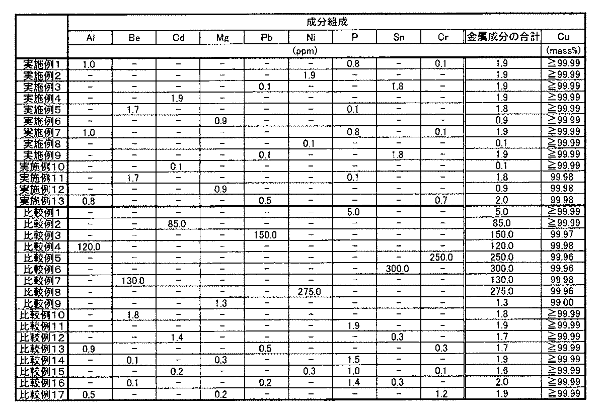
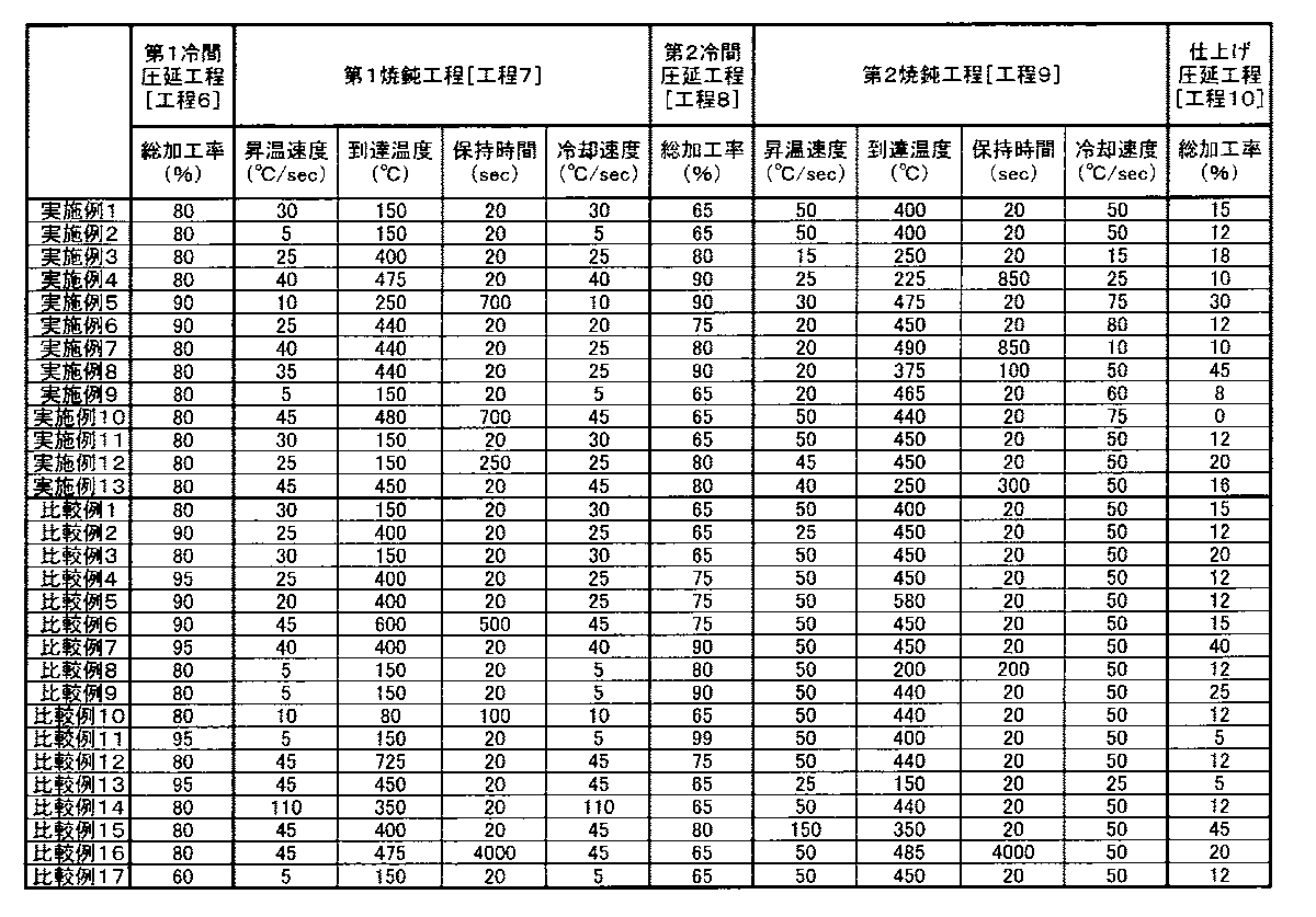
- Examples 1 to 13 and Comparative Examples 1 to 17 First, a copper material having the component composition shown in Table 1 was melted and cast to obtain an ingot [Step 1]. The resulting ingot was subjected to a homogenization heat treatment at a holding temperature of 700 to 1000 ° C. and a holding time of 10 minutes to 20 hours [Step 2]. Then, hot rolling was performed so that the total processing rate became 10 to 90% [Step 3], and then rapid cooling was performed at a cooling rate of 10 ° C./sec or more [Step 4]. Both sides of the cooled material were chamfered by about 1.0 mm each [Step 5].
- the first annealing was carried out at the rate of temperature rise, ultimate temperature, holding time and cooling rate shown in Table 2 [Step] 7].
- the second cold rolling was performed at the total processing rate shown in Table 2 [Step 8]
- the second annealing was performed at the rate of temperature rise, ultimate temperature, holding time and cooling rate shown in Table 2 [Step 9].
- finish rolling was performed at the total processing rate shown in Table 2 [Step 10].
- pickling and polishing were performed [Step 12] to produce a copper plate material (test material).
- Table 3 shows the average value of the orientation density in the range A and the maximum value of the orientation density in the range B for each specimen.
- ⁇ Average crystal grain size> The average crystal grain size was measured by the same method as the orientation density. The average crystal grain size was calculated from all the crystal grains included in the measurement range. Table 3 shows the average crystal grain size of each test material.
- ⁇ Conductivity> The conductivity was calculated from the value of the specific resistance measured by the four probe method in a thermostat kept at 20 ° C. ( ⁇ 0.5 ° C.). In addition, the distance between terminals was 100 mm. A case where the conductivity was 95% IACS or higher was evaluated as “good”, and a case where the conductivity was lower than 95% IACS was evaluated as “bad”. Table 3 shows the conductivity of each sample material.
- ⁇ Tensile strength> Three test pieces of JIS Z2201-13B were cut out from the RD direction of each test material. The tensile strength of each test piece was measured according to JIS Z2241, and the average value was calculated. The case where the tensile strength was 150 MPa or more and 330 MPa or less was evaluated as “good”, and the case where it was less than 150 MPa or exceeding 330 MPa was evaluated as “bad”. Table 3 shows the tensile strength of each specimen.
- the total content of metal components selected from the group consisting of Al, Be, Cd, Mg, Pb, Ni, P, Sn, and Cr is 0.
- the composition had a composition of 1 to 2.0 ppm and a copper content of 99.96 mass% or more.
- the average value of the longitudinal elastic modulus from the RD direction to the TD direction was as low as 115 GPa or less, the tensile strength was 150 to 330 MPa, and the conductivity was as high as 95% IACS or more. Moreover, since the average crystal grain size after performing the heat processing for 5 hours at 800 degreeC was 200 micrometers or less, it turned out that the growth of a crystal grain is suppressed.
- the average value of the longitudinal elastic modulus from the RD direction to the TD direction was as high as 135 GPa and 150 GPa, respectively. Further, the average crystal grain size after heat treatment at 800 ° C. for 5 hours was as large as 368 ⁇ m and 399 ⁇ m, respectively, and the growth of crystal grains was confirmed.
- the maximum value of density was as high as 35.0. Therefore, the average crystal grain size after heat treatment at 800 ° C. for 5 hours was as large as 456 ⁇ m, and the growth of crystal grains was confirmed.
- the copper plate material of the present invention has a low longitudinal elastic modulus continuously from the rolling direction to the plate width direction, and is excellent in tensile strength and electrical conductivity. Moreover, since the growth of crystal grains is suppressed when the copper plate material of the present invention is heat-treated at a high temperature, peeling or the like hardly occurs at the joint portion with the ceramic substrate. Therefore, the copper plate material of the present invention is excellent for an insulating substrate with a copper plate.
Landscapes
- Chemical & Material Sciences (AREA)
- Engineering & Computer Science (AREA)
- Materials Engineering (AREA)
- Organic Chemistry (AREA)
- Mechanical Engineering (AREA)
- Metallurgy (AREA)
- Physics & Mathematics (AREA)
- Thermal Sciences (AREA)
- Crystallography & Structural Chemistry (AREA)
- Ceramic Engineering (AREA)
- Structural Engineering (AREA)
- Conductive Materials (AREA)
- Non-Insulated Conductors (AREA)
Abstract
Description
(1)Al、Be、Cd、Mg、Pb、Ni、P、Sn及びCrからなる群から選択される金属成分の合計含有量が0.1~2.0ppm、銅の含有量が99.96mass%以上である組成を有し、かつ、EBSDによる集合組織解析から得られた結晶方位分布関数をオイラー角(φ1、Φ、φ2)で表したとき、φ2=0°、φ1=0°、Φ=0°~90°の範囲における方位密度の平均値が3.0以上35.0未満であり、かつ、φ2=35°、φ1=45°~55°、Φ=65°~80°の範囲における方位密度の最大値が1.0以上30.0未満である圧延集合組織を有する、銅板付き絶縁基板用銅板材。
(2)前記銅の含有量が99.99mass%以上であり、かつ、縦弾性係数の平均値が115GPa以下であり、前記縦弾性係数は、圧延方向、板幅方向、及びこれらの間の方向で測定される、(1)に記載の銅板付き絶縁基板用銅板材。
(3)平均結晶粒径が3μm~100μmである、(1)又は(2)に記載の銅板付き絶縁基板用銅板材。
(4)700~800℃で10分~5時間の熱履歴を受けた状態で、平均結晶粒径が50μm~200μmである、(1)から(3)のいずれかに記載の銅板付き絶縁基板用銅板材。
(5)引張強度が150~330MPaであり、かつ、導電率が95%IACS以上である、(1)から(4)のいずれかに記載の銅板付き絶縁基板用銅板材。
(6)(1)から(5)のいずれかに記載の銅板付き絶縁基板用銅板材の製造方法であって、
前記組成を有する銅素材を鋳造して得られた鋳塊に対して均質化熱処理を行う均質化熱処理工程と、
該均質化熱処理工程後に、熱間圧延を行う熱間圧延工程と、
該熱間圧延工程後に、冷却を行う冷却工程と、
該冷却工程後の被圧延材の両面を面削する面削工程と、
該面削工程後に、総加工率が75%以上である冷間圧延を行う第1冷間圧延工程と、
該第1冷間圧延工程後に、昇温速度が1~100℃/秒、到達温度が100~500℃、保持時間が1~900秒、かつ、冷却速度が1~50℃/秒である条件で熱処理を施す第1焼鈍工程と、
該第1焼鈍工程後に、総加工率が60~95%である冷間圧延を行う第2冷間圧延工程と、
該第2冷間圧延工程後に、昇温速度が10~100℃/秒、到達温度が200~550℃、保持時間が10~3600秒、かつ、冷却速度が10~100℃/秒である条件で熱処理を施す第2焼鈍工程と、
該第2焼鈍工程後に、さらなる圧延を行う仕上げ圧延工程と、
該仕上げ圧延工程後に、最終熱処理を施す最終焼鈍工程と、
該最終焼鈍工程後に、酸洗及び研磨を行う表面酸化膜除去工程と、
を含む、銅板付き絶縁基板用銅板材の製造方法。
銅の含有量は、99.96mass%以上であり、好ましくは99.99mass%以上である。銅の含有量が99.96mass%未満であると、熱伝導率が低下し、所望する放熱性が得られない。また、Al、Be、Cd、Mg、Pb、Ni、P、Sn及びCrからなる群から選択される金属成分の合計含有量が0.1~2.0ppmであり、0.1~1.0ppmであることが好ましい。これらの金属成分の合計含有量の下限値は、特に限定されるものではないが、不可避的不純物を考慮し、0.1ppmである。一方、これらの金属成分の合計含有量が2.0ppmを超えると、所望の方位密度が得られない。また、銅板材には、銅、並びに、Al、Be、Cd、Mg、Pb、Ni、P、Sn及びCrからなる群から選択される金属成分以外に、残部として不可避的不純物が含まれていてもよい。不可避的不純物は、製造工程上、不可避的に含まれうる含有レベルの不純物を意味する。
本発明の銅板材は、圧延集合組織を有し、この圧延集合組織は、EBSDによる集合組織解析から得られた結晶方位分布関数(ODF:crystal orientation distribution function)をオイラー角(φ1、Φ、φ2)で表したとき、φ2=0°、φ1=0°、Φ=0°~90°の範囲における方位密度の平均値が3.0以上35.0未満、好ましくは15以下であり、かつ、φ2=35°、φ1=45°~55°、Φ=65°~80°の範囲における方位密度の最大値が1.0以上30.0未満、好ましくは10以上である。圧延方向をRD方向、板幅方向(RD方向に対して直交する方向)をTD方向、圧延面(RD面)に対して垂直な方向をND方向としたとき、RD方向を軸とした方位回転がΦ、ND方向を軸とした方位回転がφ1、TD方向を軸とした方位回転がφ2として表される。方位密度は、集合組織における結晶方位の存在比率及び分散状態を定量的に解析する際に用いられるパラメータであり、EBSD及びX線回折を行い、(100)、(110)、(112)等の3種類以上の正極点図の測定データに基づいて、級数展開法による結晶方位分布解析法により算出される。EBSDによる集合組織解析から得られる、φ2を所定の角度で固定した断面図において、RD面内での方位密度の分布が示される。
縦弾性係数の平均値は、115GPa以下であることが好ましく、110GPa以下であることがより好ましい。また、縦弾性係数の平均値の下限値は、80GPa以上であることが好ましい。縦弾性係数は、RD方向、TD方向、及びこれらの間の方向で測定される。具体的に、縦弾性係数の平均値は、RD方向からTD方向に向かって所定の角度(例えば、10°)ずつ回転した、それぞれの方向での縦弾性係数を算出した後、それらの平均値を算出することにより得られる。上記範囲で測定した縦弾性係数の平均値が115GPaを超えると、絶縁基板と接合するために熱処理を行う場合に熱膨張による負荷応力が高くなる傾向になる。
本発明の銅板材において、平均結晶粒径は3μm~100μmであることが好ましく、10μm~90μm以下であることがより好ましい。平均結晶粒径が3μm未満であると、十分な結晶方位制御ができない場合がある。一方、平均結晶粒径が100μmを超えると、引張強度が低下する傾向にある。また、700~800℃で10分~5時間の熱履歴を受けた状態で、平均結晶粒径は50μm~200μmであることが好ましいく、120μm以上であることがより好ましい。熱履歴を受けた状態における平均結晶粒径が200μmを超えると、ボンディング性の低下、熱膨張時の負荷が大きくなる。なお、結晶粒径は、銅板材のRD面におけるEBSD解析により測定することができる。熱履歴を受けた状態における結晶粒径も、銅板材に対して熱処理を行った後、同様の方法で測定することができる。
本発明の銅板材において、引張強度は150~330MPaであることが好ましく、190MPa以上であることが好ましい。引張強度が150MPa未満であると、強度が不十分であり、引張強度が330MPaを超えると、伸び、加工性が低下する傾向にある。また、導電率は95%IACS以上であることが好ましい。導電率が95%未満であると、熱伝導率が低下し、その結果、放熱性が劣化する傾向にある。
次に、本発明の銅板材の製造方法の一例を説明する。
式中、t0は圧延前の板厚であり、tは圧延後の板厚である。
まず、表1に示す成分組成を有する銅素材を溶解し、鋳造して鋳塊を得た[工程1]。得られた鋳塊に対して、保持温度700~1000℃、保持時間10分~20時間の均質化熱処理を行った[工程2]。そして、総加工率が10~90%となるように熱間圧延を行った[工程3]後、10℃/sec以上の冷却速度で急冷を行った[工程4]。冷却された材料の両面をそれぞれ約1.0mmずつ面削した[工程5]。次に、表2に示す総加工率で第1冷間処理を行った[工程6]後、表2に示す昇温速度、到達温度、保持時間及び冷却速度で第1焼鈍を行った[工程7]。次に、表2に示す総加工率で第2冷間圧延を行った[工程8]表2に示す昇温速度、到達温度、保持時間及び冷却速度で第2焼鈍を行った[工程9]後、表2に示す総加工率で仕上げ圧延を行った[工程10]。到達温度が125~400℃である条件で最終焼鈍を行った[工程11]後、酸洗及び研磨を行い[工程12]、銅板材(供試材)を作製した。
<金属成分の定量分析>
作製した各供試材について、VG 9000(VG Scientific社製)を用いて解析を行った。各供試材に含まれるAl、Be、Cd、Mg、Pb、Ni、P、Sn及びCrの含有量(ppm)、Al、Be、Cd、Mg、Pb、Ni、P、Sn及びCr(表1では単に「金属成分」と記す)の合計含有量(ppm)、並びにCuの含有量(mass%)を表1に示す。なお、各供試材には、不可避的不純物が含まれている場合がある。また、表1における「-」は、該当する金属成分が検出されなかったことを意味する。
方位密度は、OIM5.0HIKARI(TSL社製)を用い、EBSD法により測定した。測定面積は、結晶粒を200個以上含む、800μm×1600μmの範囲とし、スキャンステップを0.1μmとした。測定後の結晶粒の解析には、TSL社製の解析ソフトOIM Analysis(商品名)を用いた。解析により得られた結晶方位分布関数はオイラー角で表示された。φ2=0°の断面図より、φ1=0°、Φ=0°~90°の範囲(表3では「範囲A」と記す)における方位密度の平均値を算出した。また、オイラー角で表示されたφ2=35°の断面図において、φ1=45°~55°、Φ=65°~80°の範囲(表3では「範囲B」と記す)における方位密度の最大値を読み出した。各供試材について、範囲Aにおける方位密度の平均値及び範囲Bにおける方位密度の最大値を表3に示す。
平均結晶粒径は、方位密度と同様の方法で測定した。測定範囲に含まれる全ての結晶粒より、平均結晶粒径を算出した。各供試材の平均結晶粒径を表3に示す。
各供試材から、RD方向と、TD方向と、RD方向からTD方向にかけて10°おきに回転させた方向において、それぞれ幅20mm、長さ200mmの短冊状試験片を採取した。まず、試験片の長さ方向に引張試験機により応力を付与した。そして、降伏するときの歪量の80%の歪量を最大変位量とし、その最大変位量までを10分割した変位を与えた。その10点で歪と応力の比例定数を算出し、各比例定数の平均値を縦弾性係数の平均値とした。縦弾性係数の平均値が115GPa以下である場合を「良好」、115GPaを超える場合を「不良」と評価した。各供試材について、縦弾性係数の平均値を表3に示す。
導電率は、20℃(±0.5℃)に保たれた恒温槽中で四端子法により計測した比抵抗の数値から算出した。なお、端子間距離は100mmとした。導電率が95%IACS以上である場合を「良好」、95%IACS未満である場合を「不良」と評価した。各供試材の導電率を表3に示す。
各供試材のRD方向から、JIS Z2201-13B号の試験片を3本切り出した。JIS Z2241に準じて、各試験片の引張強度を測定し、その平均値を算出した。引張強度が150MPa以上330MPa以下である場合を「良好」、150MPa未満である場合又は330MPaを超える場合を「不良」と評価した。各供試材の引張強度を表3に示す。
各供試材に対して、アルゴン雰囲気又は窒素雰囲気下の管状炉で800℃で5時間の熱処理を施した後、上記平均結晶粒径の測定方法と同様の方法で、平均結晶粒径を測定した。熱処理後の平均結晶粒径が200μm以下である場合を耐熱性が「良好」、200μmを超える場合を耐熱性が「不良」と評価した。各供試材について、熱処理後の平均結晶粒径を表3に示す。一般的に、結晶粒径は、熱処理を高温で長時間行うほど成長する。すなわち、800℃で5時間の熱処理を行った後に平均結晶粒径が200μm以下である供試材については、700~800℃で10分以上5時間以内の熱処理を行った場合に、平均結晶粒径が200μm以下であることは自明である。

Claims (6)
- Al、Be、Cd、Mg、Pb、Ni、P、Sn及びCrからなる群から選択される金属成分の合計含有量が0.1~2.0ppm、銅の含有量が99.96mass%以上である組成を有し、かつ、EBSDによる集合組織解析から得られた結晶方位分布関数をオイラー角(φ1、Φ、φ2)で表したとき、φ2=0°、φ1=0°、Φ=0°~90°の範囲における方位密度の平均値が3.0以上35.0未満であり、かつ、φ2=35°、φ1=45°~55°、Φ=65°~80°の範囲における方位密度の最大値が1.0以上30.0未満である圧延集合組織を有することを特徴とする銅板付き絶縁基板用銅板材。
- 前記銅の含有量が99.99mass%以上であり、かつ、縦弾性係数の平均値が115GPa以下であり、前記縦弾性係数は圧延方向、板幅方向、及びこれらの間の方向で測定される、請求項1に記載の銅板付き絶縁基板用銅板材。
- 平均結晶粒径が3μm~100μmである、請求項1又は2に記載の銅板付き絶縁基板用銅板材。
- 700~800℃で10分~5時間の熱履歴を受けた状態で、平均結晶粒径が50μm~200μmである、請求項1から3までのいずれか1項に記載の銅板付き絶縁基板用銅板材。
- 引張強度が150~330MPaであり、かつ、導電率が95%IACS以上である、請求項1から4までのいずれか1項に記載の銅板付き絶縁基板用銅板材。
- 請求項1から5までのいずれか1項に記載の銅板付き絶縁基板用銅板材の製造方法であって、
前記組成を有する銅素材を鋳造して得られた鋳塊に対して均質化熱処理を行う均質化熱処理工程と、
該均質化熱処理工程後に、熱間圧延を行う熱間圧延工程と、
該熱間圧延工程後に、冷却を行う冷却工程と、
該冷却工程後の被圧延材の両面を面削する面削工程と、
該面削工程後に、総加工率が75%以上である冷間圧延を行う第1冷間圧延工程と、
該第1冷間圧延工程後に、昇温速度が1~100℃/秒、到達温度が100~500℃、保持時間が1~900秒、かつ、冷却速度が1~50℃/秒である条件で熱処理を施す第1焼鈍工程と、
該第1焼鈍工程後に、総加工率が60~95%である冷間圧延を行う第2冷間圧延工程と、
該第2冷間圧延工程後に、昇温速度が10~100℃/秒、到達温度が200~550℃、保持時間が10~3600秒、かつ、冷却速度が10~100℃/秒である条件で熱処理を施す第2焼鈍工程と、
該第2焼鈍工程後に、さらなる圧延を行う仕上げ圧延工程と、
該仕上げ圧延工程後に、最終熱処理を施す最終焼鈍工程と、
該最終焼鈍工程後に、酸洗及び研磨を行う表面酸化膜除去工程と、
を含む、銅板付き絶縁基板用銅板材の製造方法。
Priority Applications (3)
| Application Number | Priority Date | Filing Date | Title |
|---|---|---|---|
| JP2018540895A JP6678757B2 (ja) | 2017-03-31 | 2018-03-28 | 銅板付き絶縁基板用銅板材及びその製造方法 |
| KR1020187026843A KR102326618B1 (ko) | 2017-03-31 | 2018-03-28 | 구리판 부착 절연 기판용 구리판재 및 그 제조 방법 |
| CN201880022820.7A CN110462074A (zh) | 2017-03-31 | 2018-03-28 | 用于带铜板的绝缘基板的铜板材及其制造方法 |
Applications Claiming Priority (2)
| Application Number | Priority Date | Filing Date | Title |
|---|---|---|---|
| JP2017-069734 | 2017-03-31 | ||
| JP2017069734 | 2017-03-31 |
Publications (1)
| Publication Number | Publication Date |
|---|---|
| WO2018181593A1 true WO2018181593A1 (ja) | 2018-10-04 |
Family
ID=63677024
Family Applications (1)
| Application Number | Title | Priority Date | Filing Date |
|---|---|---|---|
| PCT/JP2018/013002 Ceased WO2018181593A1 (ja) | 2017-03-31 | 2018-03-28 | 銅板付き絶縁基板用銅板材及びその製造方法 |
Country Status (4)
| Country | Link |
|---|---|
| JP (1) | JP6678757B2 (ja) |
| KR (1) | KR102326618B1 (ja) |
| CN (1) | CN110462074A (ja) |
| WO (1) | WO2018181593A1 (ja) |
Cited By (12)
| Publication number | Priority date | Publication date | Assignee | Title |
|---|---|---|---|---|
| WO2019138971A1 (ja) * | 2018-01-10 | 2019-07-18 | 古河電気工業株式会社 | 絶縁電線 |
| JP6582159B1 (ja) * | 2018-03-29 | 2019-09-25 | 古河電気工業株式会社 | 絶縁基板及びその製造方法 |
| WO2020122112A1 (ja) * | 2018-12-13 | 2020-06-18 | 三菱マテリアル株式会社 | 純銅板 |
| WO2021145148A1 (ja) * | 2020-01-15 | 2021-07-22 | 古河電気工業株式会社 | 銅板材およびその製造方法、ならびに銅板材付き絶縁基板 |
| WO2021177460A1 (ja) * | 2020-03-06 | 2021-09-10 | 三菱マテリアル株式会社 | 純銅板、銅/セラミックス接合体、絶縁回路基板 |
| WO2021177461A1 (ja) * | 2020-03-06 | 2021-09-10 | 三菱マテリアル株式会社 | 純銅板、銅/セラミックス接合体、絶縁回路基板 |
| WO2022085723A1 (ja) * | 2020-10-23 | 2022-04-28 | 三菱マテリアル株式会社 | スリット銅材、電子・電気機器用部品、バスバー、放熱基板 |
| WO2022085718A1 (ja) * | 2020-10-23 | 2022-04-28 | 三菱マテリアル株式会社 | スリット銅材、電子・電気機器用部品、バスバー、放熱基板 |
| JP2022069414A (ja) * | 2020-10-23 | 2022-05-11 | 三菱マテリアル株式会社 | スリット銅材、電子・電気機器用部品、バスバー、放熱基板 |
| JP2022069413A (ja) * | 2020-10-23 | 2022-05-11 | 三菱マテリアル株式会社 | スリット銅材、電子・電気機器用部品、バスバー、放熱基板 |
| JP2025094030A (ja) * | 2020-03-10 | 2025-06-24 | 株式会社プロテリアル | セラミックス回路基板 |
| WO2026094998A1 (ja) * | 2024-11-01 | 2026-05-07 | 三菱マテリアル株式会社 | 銅材料、および、絶縁基板 |
Families Citing this family (3)
| Publication number | Priority date | Publication date | Assignee | Title |
|---|---|---|---|---|
| US12331386B2 (en) | 2020-03-06 | 2025-06-17 | Mitsubishi Materials Corporation | Pure copper plate |
| JP7791019B2 (ja) * | 2022-03-14 | 2025-12-23 | Dowaメタルテック株式会社 | 銅-セラミックス接合基板およびその製造方法 |
| CN121222858A (zh) * | 2025-10-17 | 2025-12-30 | 江西铜业集团铜板带有限公司 | 一种高精密汽车连接器紫铜带的制备方法 |
Citations (3)
| Publication number | Priority date | Publication date | Assignee | Title |
|---|---|---|---|---|
| JP2009102690A (ja) * | 2007-10-23 | 2009-05-14 | Kobelco & Materials Copper Tube Inc | 破壊強度に優れた熱交換器用銅合金管 |
| WO2016171054A1 (ja) * | 2015-04-24 | 2016-10-27 | 古河電気工業株式会社 | 銅合金板材およびその製造方法 |
| JP2018016823A (ja) * | 2016-07-25 | 2018-02-01 | 古河電気工業株式会社 | 放熱部材用銅合金板材およびその製造方法 |
Family Cites Families (9)
| Publication number | Priority date | Publication date | Assignee | Title |
|---|---|---|---|---|
| JP4563495B1 (ja) * | 2009-04-27 | 2010-10-13 | Dowaメタルテック株式会社 | 銅合金板材およびその製造方法 |
| JP5961335B2 (ja) * | 2010-04-05 | 2016-08-02 | Dowaメタルテック株式会社 | 銅合金板材および電気・電子部品 |
| CN103703154B (zh) * | 2011-08-04 | 2015-11-25 | 株式会社神户制钢所 | 铜合金 |
| JP6256733B2 (ja) * | 2012-02-29 | 2018-01-10 | 日立金属株式会社 | セラミックス回路基板の製造方法およびセラミックス回路基板 |
| JP5991103B2 (ja) * | 2012-09-14 | 2016-09-14 | 三菱マテリアル株式会社 | ヒートシンク付パワーモジュール用基板、ヒートシンク付パワーモジュール、及びヒートシンク付パワーモジュール用基板の製造方法 |
| JP5475914B1 (ja) | 2012-09-28 | 2014-04-16 | Jx日鉱日石金属株式会社 | 放熱性及び繰り返し曲げ加工性に優れた銅合金板 |
| JP5619977B2 (ja) * | 2012-09-28 | 2014-11-05 | Jx日鉱日石金属株式会社 | 放熱性及び繰り返し曲げ加工性に優れた銅合金板 |
| JP6202718B2 (ja) | 2013-03-26 | 2017-09-27 | 三菱マテリアル株式会社 | 放熱基板 |
| CN105568047B (zh) * | 2015-12-29 | 2017-10-10 | 宁波博威合金材料股份有限公司 | 高强高弹高导铜合金 |
-
2018
- 2018-03-28 CN CN201880022820.7A patent/CN110462074A/zh active Pending
- 2018-03-28 KR KR1020187026843A patent/KR102326618B1/ko active Active
- 2018-03-28 JP JP2018540895A patent/JP6678757B2/ja active Active
- 2018-03-28 WO PCT/JP2018/013002 patent/WO2018181593A1/ja not_active Ceased
Patent Citations (3)
| Publication number | Priority date | Publication date | Assignee | Title |
|---|---|---|---|---|
| JP2009102690A (ja) * | 2007-10-23 | 2009-05-14 | Kobelco & Materials Copper Tube Inc | 破壊強度に優れた熱交換器用銅合金管 |
| WO2016171054A1 (ja) * | 2015-04-24 | 2016-10-27 | 古河電気工業株式会社 | 銅合金板材およびその製造方法 |
| JP2018016823A (ja) * | 2016-07-25 | 2018-02-01 | 古河電気工業株式会社 | 放熱部材用銅合金板材およびその製造方法 |
Cited By (33)
| Publication number | Priority date | Publication date | Assignee | Title |
|---|---|---|---|---|
| US11437167B2 (en) | 2018-01-10 | 2022-09-06 | Essex Furukawa Magnet Wire Japan Co., Ltd. | Insulated wire |
| WO2019138971A1 (ja) * | 2018-01-10 | 2019-07-18 | 古河電気工業株式会社 | 絶縁電線 |
| JPWO2019138971A1 (ja) * | 2018-01-10 | 2021-01-14 | 古河電気工業株式会社 | 絶縁電線 |
| JP7233820B2 (ja) | 2018-01-10 | 2023-03-07 | エセックス古河マグネットワイヤジャパン株式会社 | 絶縁電線 |
| JP6582159B1 (ja) * | 2018-03-29 | 2019-09-25 | 古河電気工業株式会社 | 絶縁基板及びその製造方法 |
| WO2019187767A1 (ja) * | 2018-03-29 | 2019-10-03 | 古河電気工業株式会社 | 絶縁基板及びその製造方法 |
| JP7380550B2 (ja) | 2018-12-13 | 2023-11-15 | 三菱マテリアル株式会社 | 純銅板 |
| CN115896532B (zh) * | 2018-12-13 | 2025-05-02 | 三菱综合材料株式会社 | 纯铜板 |
| JPWO2020122112A1 (ja) * | 2018-12-13 | 2021-09-02 | 三菱マテリアル株式会社 | 純銅板 |
| KR102872450B1 (ko) * | 2018-12-13 | 2025-10-16 | 미쓰비시 마테리알 가부시키가이샤 | 순구리판 |
| US12385110B2 (en) | 2018-12-13 | 2025-08-12 | Mitsubishi Materials Corporation | Pure copper plate |
| CN112969805A (zh) * | 2018-12-13 | 2021-06-15 | 三菱综合材料株式会社 | 纯铜板 |
| TWI892973B (zh) * | 2018-12-13 | 2025-08-11 | 日商三菱綜合材料股份有限公司 | 純銅板 |
| CN115896532A (zh) * | 2018-12-13 | 2023-04-04 | 三菱综合材料株式会社 | 纯铜板 |
| KR20210102191A (ko) * | 2018-12-13 | 2021-08-19 | 미쓰비시 마테리알 가부시키가이샤 | 순구리판 |
| WO2020122112A1 (ja) * | 2018-12-13 | 2020-06-18 | 三菱マテリアル株式会社 | 純銅板 |
| JP2023120449A (ja) * | 2018-12-13 | 2023-08-29 | 三菱マテリアル株式会社 | 純銅板 |
| EP3896179A4 (en) * | 2018-12-13 | 2022-10-19 | Mitsubishi Materials Corporation | PURE COPPER PLATE |
| WO2021145148A1 (ja) * | 2020-01-15 | 2021-07-22 | 古河電気工業株式会社 | 銅板材およびその製造方法、ならびに銅板材付き絶縁基板 |
| JP6982710B1 (ja) * | 2020-01-15 | 2021-12-17 | 古河電気工業株式会社 | 銅板材およびその製造方法、ならびに銅板材付き絶縁基板 |
| US12035469B2 (en) | 2020-03-06 | 2024-07-09 | Mitsubishi Materials Corporation | Pure copper plate, copper/ceramic bonded body, and insulated circuit board |
| JP6984799B1 (ja) * | 2020-03-06 | 2021-12-22 | 三菱マテリアル株式会社 | 純銅板、銅/セラミックス接合体、絶縁回路基板 |
| WO2021177461A1 (ja) * | 2020-03-06 | 2021-09-10 | 三菱マテリアル株式会社 | 純銅板、銅/セラミックス接合体、絶縁回路基板 |
| WO2021177460A1 (ja) * | 2020-03-06 | 2021-09-10 | 三菱マテリアル株式会社 | 純銅板、銅/セラミックス接合体、絶縁回路基板 |
| JP2025094030A (ja) * | 2020-03-10 | 2025-06-24 | 株式会社プロテリアル | セラミックス回路基板 |
| JP2022069413A (ja) * | 2020-10-23 | 2022-05-11 | 三菱マテリアル株式会社 | スリット銅材、電子・電気機器用部品、バスバー、放熱基板 |
| JP7342924B2 (ja) | 2020-10-23 | 2023-09-12 | 三菱マテリアル株式会社 | スリット銅材、電子・電気機器用部品、バスバー、放熱基板 |
| JP7342923B2 (ja) | 2020-10-23 | 2023-09-12 | 三菱マテリアル株式会社 | スリット銅材、電子・電気機器用部品、バスバー、放熱基板 |
| JP2022069414A (ja) * | 2020-10-23 | 2022-05-11 | 三菱マテリアル株式会社 | スリット銅材、電子・電気機器用部品、バスバー、放熱基板 |
| WO2022085718A1 (ja) * | 2020-10-23 | 2022-04-28 | 三菱マテリアル株式会社 | スリット銅材、電子・電気機器用部品、バスバー、放熱基板 |
| US12281376B2 (en) * | 2020-10-23 | 2025-04-22 | Mitsubishi Materials Corporation | Slit copper material, part for electric/electronic device, bus bar, heat dissipation substrate |
| WO2022085723A1 (ja) * | 2020-10-23 | 2022-04-28 | 三菱マテリアル株式会社 | スリット銅材、電子・電気機器用部品、バスバー、放熱基板 |
| WO2026094998A1 (ja) * | 2024-11-01 | 2026-05-07 | 三菱マテリアル株式会社 | 銅材料、および、絶縁基板 |
Also Published As
| Publication number | Publication date |
|---|---|
| CN110462074A (zh) | 2019-11-15 |
| JPWO2018181593A1 (ja) | 2020-02-06 |
| KR102326618B1 (ko) | 2021-11-16 |
| JP6678757B2 (ja) | 2020-04-08 |
| KR20190134455A (ko) | 2019-12-04 |
Similar Documents
| Publication | Publication Date | Title |
|---|---|---|
| JP6678757B2 (ja) | 銅板付き絶縁基板用銅板材及びその製造方法 | |
| TWI433939B (zh) | Cu-Mg-P系銅合金條材料及其製造方法 | |
| TWI480394B (zh) | Cu-Mg-P copper alloy strip and its manufacturing method | |
| KR101136265B1 (ko) | 전기 전자 부품용 구리 합금판 | |
| EP3922391A1 (en) | Production method for copper/ceramic joined body, production method for insulated circuit board, copper/ceramic joined body, and insulated circuit board | |
| JP6719316B2 (ja) | 放熱部材用銅合金板材およびその製造方法 | |
| JPWO2019244842A1 (ja) | 抵抗器用抵抗材料およびその製造方法並びに抵抗器 | |
| JP6472477B2 (ja) | Cu−Ni−Si系銅合金条 | |
| JP7833550B2 (ja) | Al接続材 | |
| CN110506132A (zh) | Cu-Co-Si系铜合金板材和制造方法以及使用了该板材的部件 | |
| US20240312946A1 (en) | Ai bonding wire for semiconductor devices | |
| KR102349545B1 (ko) | 구리 합금 선봉재 및 그 제조 방법 | |
| JP2017150015A (ja) | スパッタリングターゲット、およびスパッタリングターゲットの製造方法 | |
| JP6582159B1 (ja) | 絶縁基板及びその製造方法 | |
| JP2015203148A (ja) | 銅合金材、セラミック配線基板及びセラミック配線基板の製造方法 | |
| TW201736612A (zh) | Cu-Ni-Si系銅合金條及其製造方法 | |
| JP7445096B1 (ja) | 銅合金板材および絞り加工部品 | |
| JP7203930B2 (ja) | 銅板材およびその製造方法、ならびに銅板材付き絶縁基板 | |
| JP6599059B1 (ja) | クラッド材及びその製造方法 | |
| JP2004002988A (ja) | 曲げ加工性に優れたりん青銅条 | |
| JP7733858B1 (ja) | Alボンディングワイヤ又はAlボンディングリボン | |
| TWI529255B (zh) | Cu-Ni-Si合金及其製造方法 | |
| JP2020158800A (ja) | 高純度アルミニウムシートおよびその製造方法ならびに当該高純度アルミニウムシートを用いたパワー半導体モジュール | |
| JP2007291516A (ja) | 銅合金とその製造方法 | |
| WO2026094998A1 (ja) | 銅材料、および、絶縁基板 |
Legal Events
| Date | Code | Title | Description |
|---|---|---|---|
| ENP | Entry into the national phase |
Ref document number: 2018540895 Country of ref document: JP Kind code of ref document: A |
|
| ENP | Entry into the national phase |
Ref document number: 20187026843 Country of ref document: KR Kind code of ref document: A |
|
| 121 | Ep: the epo has been informed by wipo that ep was designated in this application |
Ref document number: 18777448 Country of ref document: EP Kind code of ref document: A1 |
|
| NENP | Non-entry into the national phase |
Ref country code: DE |
|
| 122 | Ep: pct application non-entry in european phase |
Ref document number: 18777448 Country of ref document: EP Kind code of ref document: A1 |