WO2018180107A1 - 湿度センサ - Google Patents
湿度センサ Download PDFInfo
- Publication number
- WO2018180107A1 WO2018180107A1 PCT/JP2018/007053 JP2018007053W WO2018180107A1 WO 2018180107 A1 WO2018180107 A1 WO 2018180107A1 JP 2018007053 W JP2018007053 W JP 2018007053W WO 2018180107 A1 WO2018180107 A1 WO 2018180107A1
- Authority
- WO
- WIPO (PCT)
- Prior art keywords
- humidity sensor
- upper electrode
- sensitive film
- moisture sensitive
- electrode
- Prior art date
- Legal status (The legal status is an assumption and is not a legal conclusion. Google has not performed a legal analysis and makes no representation as to the accuracy of the status listed.)
- Ceased
Links
Images















Classifications
-
- G—PHYSICS
- G01—MEASURING; TESTING
- G01N—INVESTIGATING OR ANALYSING MATERIALS BY DETERMINING THEIR CHEMICAL OR PHYSICAL PROPERTIES
- G01N27/00—Investigating or analysing materials by the use of electric, electrochemical, or magnetic means
- G01N27/02—Investigating or analysing materials by the use of electric, electrochemical, or magnetic means by investigating impedance
- G01N27/04—Investigating or analysing materials by the use of electric, electrochemical, or magnetic means by investigating impedance by investigating resistance
- G01N27/048—Investigating or analysing materials by the use of electric, electrochemical, or magnetic means by investigating impedance by investigating resistance for determining moisture content of the material
-
- G—PHYSICS
- G01—MEASURING; TESTING
- G01N—INVESTIGATING OR ANALYSING MATERIALS BY DETERMINING THEIR CHEMICAL OR PHYSICAL PROPERTIES
- G01N27/00—Investigating or analysing materials by the use of electric, electrochemical, or magnetic means
- G01N27/02—Investigating or analysing materials by the use of electric, electrochemical, or magnetic means by investigating impedance
- G01N27/22—Investigating or analysing materials by the use of electric, electrochemical, or magnetic means by investigating impedance by investigating capacitance
- G01N27/223—Investigating or analysing materials by the use of electric, electrochemical, or magnetic means by investigating impedance by investigating capacitance for determining moisture content, e.g. humidity
-
- G—PHYSICS
- G01—MEASURING; TESTING
- G01N—INVESTIGATING OR ANALYSING MATERIALS BY DETERMINING THEIR CHEMICAL OR PHYSICAL PROPERTIES
- G01N27/00—Investigating or analysing materials by the use of electric, electrochemical, or magnetic means
- G01N27/02—Investigating or analysing materials by the use of electric, electrochemical, or magnetic means by investigating impedance
- G01N27/22—Investigating or analysing materials by the use of electric, electrochemical, or magnetic means by investigating impedance by investigating capacitance
- G01N27/227—Sensors changing capacitance upon adsorption or absorption of fluid components, e.g. electrolyte-insulator-semiconductor sensors, MOS capacitors
-
- H—ELECTRICITY
- H10—SEMICONDUCTOR DEVICES; ELECTRIC SOLID-STATE DEVICES NOT OTHERWISE PROVIDED FOR
- H10D—INORGANIC ELECTRIC SEMICONDUCTOR DEVICES
- H10D1/00—Resistors, capacitors or inductors
- H10D1/60—Capacitors
- H10D1/68—Capacitors having no potential barriers
- H10D1/692—Electrodes
-
- H—ELECTRICITY
- H10—SEMICONDUCTOR DEVICES; ELECTRIC SOLID-STATE DEVICES NOT OTHERWISE PROVIDED FOR
- H10P—GENERIC PROCESSES OR APPARATUS FOR THE MANUFACTURE OR TREATMENT OF DEVICES COVERED BY CLASS H10
- H10P50/00—Etching of wafers, substrates or parts of devices
- H10P50/20—Dry etching; Plasma etching; Reactive-ion etching
- H10P50/28—Dry etching; Plasma etching; Reactive-ion etching of insulating materials
-
- G—PHYSICS
- G01—MEASURING; TESTING
- G01N—INVESTIGATING OR ANALYSING MATERIALS BY DETERMINING THEIR CHEMICAL OR PHYSICAL PROPERTIES
- G01N2201/00—Features of devices classified in G01N21/00
Definitions
- the present invention relates to a humidity sensor.
- sensors such as humidity sensors, temperature sensors, gas sensors, and capacitive touch sensors
- humidity sensors such as humidity sensors, temperature sensors, gas sensors, and capacitive touch sensors
- capacitive touch sensors are used in a wide variety of products for industrial or personal use.
- the operation of the sensor is affected, so that defensive measures against condensation and water droplets are taken.
- a configuration in which the upper electrode is covered with a protective film is known (see, for example, Patent Document 1).
- Patent Document 1 a configuration in which the upper electrode is covered with a protective film is known (see, for example, Patent Document 1).
- an opening for exposing the moisture sensitive film to the outside is formed in the protective film and the upper electrode, and the moisture sensitive film is provided at a position higher than the position of the lower surface of the protective film in the opening.
- the present invention has been made in view of the above points, and it is therefore an object of the present invention to provide a humidity sensor capable of suppressing the influence of water droplets on the humidity sensor and outputting a stable measurement value with high accuracy.
- a humidity sensor (10A, 10B) includes a lower electrode (13) formed on a substrate (11) and a first electrode covering the lower electrode (13).
- a second moisture sensitive film (19) connected to the first moisture sensitive film (15) at the opening (17a) of (17), and the area of the upper electrode (17) is It is larger than the area of the lower electrode (13) and smaller than the area of the first moisture sensitive film (15).
- the disclosed humidity sensor it is possible to prevent the influence of water droplets on the humidity sensor and output a stable measurement value with high accuracy.
- Diagram for explaining the detection principle of the humidity sensor (1) Diagram for explaining the detection principle of the humidity sensor (2) Schematic sectional view showing a humidity sensor according to the first embodiment The figure which shows an example of the electrode pattern of the humidity sensor which concerns on 1st Embodiment. The figure which shows another example of the electrode pattern of the humidity sensor which concerns on 1st Embodiment.
- Process sectional drawing for demonstrating the manufacturing method of the humidity sensor which concerns on 1st Embodiment (1) Process sectional drawing for demonstrating the manufacturing method of the humidity sensor which concerns on 1st Embodiment (1) Process sectional drawing for demonstrating the manufacturing method of the humidity sensor which concerns on 1st Embodiment (1) Process sectional drawing for demonstrating the manufacturing method of the humidity sensor which concerns on 1st Embodiment (1) Process sectional drawing for demonstrating the manufacturing method of the humidity sensor which concerns on 1st Embodiment (1) Sectional drawing (2) for demonstrating the manufacturing method of the humidity sensor which concerns on 1st Embodiment. Sectional drawing (2) for demonstrating the manufacturing method of the humidity sensor which concerns on 1st Embodiment. Sectional drawing (2) for demonstrating the manufacturing method of the humidity sensor which concerns on 1st Embodiment.
- Process sectional drawing for demonstrating the manufacturing method of the humidity sensor which concerns on 1st Embodiment (3) Process sectional drawing for demonstrating the manufacturing method of the humidity sensor which concerns on 1st Embodiment (3)
- Process sectional drawing for demonstrating the manufacturing method of the humidity sensor which concerns on 1st Embodiment (3) Diagram for explaining the humidity sensor mounted on the mounting board Diagram for explaining humidity sensor mounted on mounting board (1)
- Figure (2) for explaining the humidity sensor mounted on the mounting board Schematic sectional view showing a humidity sensor according to the second embodiment Process sectional drawing for demonstrating the manufacturing method of the humidity sensor which concerns on 2nd Embodiment (1).
- Process sectional drawing for demonstrating the manufacturing method of the humidity sensor which concerns on 2nd Embodiment (1) Process sectional drawing for demonstrating the manufacturing method of the humidity sensor which concerns on 2nd Embodiment (1). Process sectional drawing for demonstrating the manufacturing method of the humidity sensor which concerns on 2nd Embodiment (1). Process sectional drawing for demonstrating the manufacturing method of the humidity sensor which concerns on 2nd Embodiment (1). Process sectional drawing for demonstrating the manufacturing method of the humidity sensor which concerns on 2nd Embodiment (2). Process sectional drawing for demonstrating the manufacturing method of the humidity sensor which concerns on 2nd Embodiment (2). Process sectional drawing for demonstrating the manufacturing method of the humidity sensor which concerns on 2nd Embodiment (2).
- Process sectional drawing for demonstrating the manufacturing method of the humidity sensor which concerns on 2nd Embodiment (2) Process sectional drawing for demonstrating the manufacturing method of the humidity sensor which concerns on 2nd Embodiment (3) Process sectional drawing for demonstrating the manufacturing method of the humidity sensor which concerns on 2nd Embodiment (3) Process sectional drawing for demonstrating the manufacturing method of the humidity sensor which concerns on 2nd Embodiment (3)
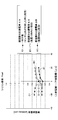
- the figure which shows the prevention effect of the influence of water adhesion in the humidity sensor which concerns on Example 1 (1)
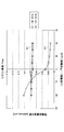
- the figure which shows the prevention effect of the influence of water adhesion in the humidity sensor which concerns on Example 1 The figure which shows the prevention effect of the influence of water adhesion in the humidity sensor which concerns on Example 1 (2)
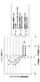
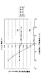
- the figure which shows the prevention effect of the influence of water adhesion in the humidity sensor which concerns on Example 2 The figure which shows the prevention effect of the influence of water adhesion in the humidity sensor which concerns on Example 2 (2)
- 1 and 2 are diagrams for explaining the principle of the humidity sensor.
- the parallel plate type humidity sensor has a structure in which a moisture sensitive film is sandwiched between a lower electrode (BE) and an upper electrode (TE).
- BE lower electrode
- TE upper electrode
- the number of water molecules adsorbed on the moisture sensitive film varies depending on the humidity, and the dielectric constant of the moisture sensitive film changes. Capturing changes in capacitance using the difference in relative permittivity of moisture sensitive film and water.
- a change in capacitance value C corresponding to a change in relative humidity (Rh) is measured between 0% and 100%.
- the approximate value is obtained by measuring the capacitance value C at a plurality of known relative humidity.
- an opening pattern may be formed in the upper electrode (TE) in order to efficiently take moisture in the air into the moisture sensitive film and enhance the response.
- the electric field leaks into the air from the opening of the upper electrode (TE).
- the state of the lines of electric force changes, and the capacitance value between the upper electrode (TE) and the lower electrode (BE) increases. Then, the original approximate expression (correction constant) cannot be used, and the function as a humidity sensor is impaired.
- a parallel plate type humidity sensor in a parallel plate type humidity sensor, a first moisture sensitive film disposed between the upper electrode and the lower electrode, and a second moisture sensitive film covering the upper electrode, Adopted a laminated structure. Further, a structure is employed in which the area of the upper electrode is larger than the area of the lower electrode and smaller than the area of the first moisture sensitive film. Thereby, the influence of the water droplet on the humidity sensor can be prevented, and a stable measurement value can be output with high accuracy.
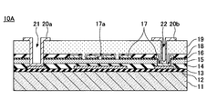
- FIG. 3 is a schematic cross-sectional view showing the humidity sensor according to the first embodiment.
- the humidity sensor 10 ⁇ / b> A has an insulating film 12, a lower electrode 13, a protective film 14, a first moisture sensitive film 15, a protective film 16, an upper electrode 17, and a protective film 18 on a substrate 11.
- the second moisture sensitive film 19 and the electrode pads 20a and 20b are stacked.
- the substrate 11 may be a semiconductor substrate such as a silicon substrate, or may be an insulating substrate.
- the insulating film 12 is formed on the substrate 11.
- the insulating film 12 may be, for example, a silicon oxide (SiO 2 ) film or a silicon nitride (SiN) film, or may be a laminated film thereof. Note that in the case where an insulating substrate is used as the substrate 11, the insulating film 12 is not necessarily provided.
- the lower electrode 13 is formed on the insulating film 12.
- the lower electrode 13 is formed in a predetermined pattern.
- the lower electrode 13 may be, for example, aluminum (Al), Al—Si, Al—Si—Cu, or may be a noble metal such as gold (Au) or platinum (Pt). Further, nickel (Ni) may be formed as these base films.
- the protective film 14 is formed so as to cover the lower electrode 13.
- the protective film 14 may be, for example, a SiO 2 film or a SiN film, or a laminated film thereof.
- the protective film 14 is not essential, but is preferably provided so as to cover the lower electrode 13 from the viewpoint of protecting the lower electrode 13 from corrosion and the like. In the case where a noble metal such as Au or Pt is used as the lower electrode 13, the protective film 14 need not be provided.
- the first moisture sensitive film 15 is formed between the lower electrode 13 and the upper electrode 17.
- the first moisture sensitive film 15 is formed of a polymer material that easily adsorbs water molecules such as polyimide (PI), cellulose, polymethyl methacrylate (PMMA), and polyvinyl alcohol (PVA).
- the thickness of the first moisture sensitive film 15 is preferably 0.5 ⁇ m or more from the viewpoint of preventing a short circuit. Further, the thickness of the first moisture sensitive film 15 is preferably 1.5 ⁇ m or less from the viewpoint of responsiveness or sensitivity. That is, the thickness of the first moisture sensitive film 15 is preferably 0.5 ⁇ m to 1.5 ⁇ m.
- the upper electrode 17 is formed on the first moisture sensitive film 15.
- the upper electrode 17 is formed in a predetermined pattern so that the area thereof is larger than the area of the lower electrode 13.
- the upper electrode 17 may be formed of the same material as that of the lower electrode 13, for example.
- the upper electrode 17 has a predetermined opening 17a, and the first moisture sensitive film 15 and the second moisture sensitive film 19 communicate with each other in the opening 17a.
- the size of the opening 17a is set to an optimum design value in consideration of characteristics and processes, but from the viewpoint that the effect of confining the leakage electric field can be sufficiently exhibited as the opening 17a is smaller, as much as possible. Smaller is preferable.
- the protective films 16 and 18 are formed so as to cover the entire circumference of the upper electrode 17. Thereby, water resistance improves.
- the protective films 16 and 18 may be, for example, a SiO 2 film or a SiN film, or may be a laminated film thereof.
- the protective films 16 and 18 are not essential, but are preferably provided so as to cover the upper electrode 17 from the viewpoint of protecting the upper electrode 17 from corrosion and the like. When a noble metal such as Au or Pt is used as the upper electrode 17, the protective films 16 and 18 may not be provided.
- the second moisture sensitive film 19 is formed so as to cover the upper electrode 17 and to be connected to the first moisture sensitive film 15 through the opening 17 a of the upper electrode 17. Thereby, even when an electric field leaks from the opening part 17a of the upper electrode 17, it can prevent that a water droplet contacts a leak electric field.
- the second moisture-sensitive film 19 may be the same type of film as the first moisture-sensitive film 15 or may be a different type of film, but from the viewpoint of moisture-sensitive characteristics, the first moisture-sensitive film 19 A film of the same type as the film 15 is preferable.
- the thickness of the second moisture sensitive film 19 is preferably equal to or greater than the thickness of the first moisture sensitive film 15 from the viewpoint of effectively preventing contact of water droplets with the leakage electric field.
- the thickness of the second moisture sensitive film 19 is not more than 10 times the thickness of the first moisture sensitive film 15 from the viewpoint of rapidly taking water molecules into the first moisture sensitive film 15. preferable. That is, the thickness of the second moisture sensitive film 19 is preferably 1 to 10 times the thickness of the first moisture sensitive film 15.
- the electrode pads 20a and 20b are pads for wire bonding.
- the electrode pad 20 a is formed in an electrode extraction opening 21 that reaches the lower electrode 13.
- the electrode pad 20 b is formed in an electrode extraction opening 22 that reaches the upper electrode 17.
- the size of the opening 21 and the opening 22 is, for example, about 40 ⁇ m to 120 ⁇ m.
- a predetermined voltage is applied between the lower electrode 13 and the upper electrode 17 via the electrode pads 20a and 20b, the capacitance value C is measured, and the relative humidity is calculated using an approximate expression (correction constant) acquired in advance. Is calculated.
- the upper electrode 17 has a leakage electric field confinement effect, and the sensor main part is protected from the adhesion of water molecules by the second moisture sensitive film 19. Is accurately converted to relative humidity.
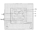
- FIG. 4 is a diagram illustrating an example of an electrode pattern of the humidity sensor 10A according to the first embodiment.
- FIG. 4 for convenience of explanation, only the lower electrode 13, the first moisture sensitive film 15, and the upper electrode 17 are illustrated, and illustration of other configurations is omitted.
- the line and space (L / S) defining the grid-like electrode pattern can be, for example, 1 ⁇ m / 1 ⁇ m, 2 ⁇ m / 2 ⁇ m, 5 ⁇ m / 5 ⁇ m, 10 ⁇ m / 10 ⁇ m.
- the area of the upper electrode 17 is larger than the area of the lower electrode 13 and smaller than the area of the first moisture sensitive film 15. Thereby, the influence of the water droplet on the humidity sensor can be prevented, and a stable measurement value can be output with high accuracy. Details will be described with reference to examples described later.
- the area of the lower electrode 13 means the area of the portion not including the extraction wiring portion
- the area of the upper electrode 17 means the area of the portion including the opening 17a and not including the extraction wiring portion.
- the cross section cut at the position of the alternate long and short dash line AA in FIG. 4 corresponds to the cross section of the humidity sensor 10A shown in FIG.
- FIG. 5 is a diagram showing another example of the electrode pattern of the humidity sensor according to the first embodiment.
- the lower electrode 13, the first moisture sensitive film 15, and the upper electrode 17 are illustrated for convenience of explanation, and illustration of other configurations is omitted.
- FIG. 5 is a ladder-like pattern formed on the first moisture sensitive film 15 on the lower electrode 13 and has an opening 17b extending in one direction.
- the second moisture sensitive film 19 is omitted for convenience of explanation, but the second moisture sensitive film 19 is disposed on the upper electrode 17, so that the leakage electric field from the opening 17 b is prevented. Water droplet contact is suppressed. At the same time, water molecules in the air can be taken in from the opening 17b to the first moisture sensitive film 15 by the shortest path.
- the line and space (L / S) defining the ladder-like electrode pattern can be set to 1 ⁇ m / 1 ⁇ m, 2 ⁇ m / 2 ⁇ m, 5 ⁇ m / 5 ⁇ m, 10 ⁇ m / 10 ⁇ m, for example.
- the area of the upper electrode 17 is larger than the area of the lower electrode 13 and smaller than the area of the first moisture sensitive film 15. Thereby, the influence of the water droplet on the humidity sensor can be prevented, and a stable measurement value can be output with high accuracy. Details will be described with reference to examples described later.
- FIGS. 3 and 4 are process cross-sectional views for explaining a method for manufacturing the humidity sensor 10A according to the first embodiment.
- the insulating film 12 is formed on the front surface and the back surface of the substrate 11. Specifically, a SiO 2 film having a thickness of 0.5 ⁇ m to 5 ⁇ m, for example, is formed on the front and back surfaces of a p-type silicon substrate by thermal oxidation. Note that the insulating film 12 may be formed only on the surface of the substrate 11 by sputtering or the like. Here, the surface of the substrate 11 means the surface on the side where the films are laminated (the upper surface in the figure).
- the lower electrode 13 is formed on the insulating film 12.
- an electrode material such as Al, Al—Si, Al—Si—Cu, Au, and Pt having a thickness of 0.2 ⁇ m, for example, is formed on the SiO 2 film, and a desired pattern is formed by photolithography. To pattern.
- a protective film 14 is formed so as to cover the lower electrode 13. Specifically, an insulating film such as a SiO 2 film, a SiN film, or a laminated film thereof is formed so as to cover the lower electrode 13. In the case where a noble metal such as Au or Pt is used as the electrode material of the lower electrode 13, the protective film 14 need not be formed.
- a first moisture sensitive film 15 is formed on the protective film 14.
- a polymer material that easily adsorbs water molecules such as PI, cellulose, PMMA, and PVA is formed on the protective film 14 by spin coating, dip, coater, etc. to a thickness of 0.5 ⁇ m to 1.5 ⁇ m. Apply to.
- a protective film 16 is formed on the first moisture sensitive film 15. Specifically, an insulating film such as a SiO 2 film, a SiN film, or a laminated film thereof is formed on the first moisture sensitive film 15. Note that when a noble metal such as Au or Pt is used as the electrode material of the upper electrode 17, the protective film 16 need not be formed.
- a resist mask having an opening at a position corresponding to the electrode outlet is formed, and the protective film 14, the first moisture sensitive film 15, and the like are formed by reactive ion etching (RIE) or the like.
- RIE reactive ion etching
- the protective film 16 is partially removed. Thereby, a part of the lower electrode 13 is exposed at a predetermined location.
- an upper electrode 17 is formed on the protective film 16.
- an electrode material such as Al, Al—Si, Al—Si—Cu, Au, and Pt having a thickness of 0.2 ⁇ m, for example, is formed on the protective film 16, and a desired pattern is formed by photolithography. To pattern. At this time, the patterning is performed so that the area of the upper electrode 17 is larger than the area of the lower electrode 13 and smaller than the area of the first moisture sensitive film 15.
- a pretreatment for example, a surface modification treatment such as plasma may be performed to improve the adhesion.
- a protective film 18 is formed so as to cover the upper electrode 17.
- an insulating film such as a SiO 2 film, a SiN film, or a laminated film thereof is formed so as to cover the upper electrode 17, and a resist mask having openings at positions corresponding to the openings 17a and the electrode outlets.
- the protective films 16 and 18 are partially removed by RIE or the like. Thereby, a part of the first moisture sensitive film 15 and the upper electrode 17 is exposed at a predetermined location.
- a noble metal such as Au or Pt is used as the electrode material of the upper electrode 17, the protective film 18 may not be formed.
- a second moisture sensitive film 19 is formed so as to cover the upper electrode 17.
- a polymer material that easily adsorbs water molecules such as PI, cellulose, PMMA, and PVA is applied to the thickness of 0.5 ⁇ m to 10 ⁇ m on the protective film 18 by spin coating, dip, coater, or the like.
- the opening 17 a of the upper electrode 17 is filled with the second moisture sensitive film 19.
- a resist mask having an opening at a position corresponding to the electrode outlet is formed, and the second moisture sensitive film 19 is partially removed by RIE or the like, so that a part of the lower electrode 13 and the upper electrode 17 is a predetermined part. Expose at points.
- an electrode extraction opening 21 reaching the lower electrode 13 and an electrode extraction opening 22 reaching the upper electrode 17 are formed.
- electrode pads 20a and 20b are formed in the opening 21 and the opening 22, respectively.
- a metal film having a thickness of 0.5 ⁇ m to 0.6 ⁇ m is formed on the openings 21 and 22 by lift-off.
- back grinding back surface polishing
- the p-type silicon substrate is thinned to a desired thickness by polishing the SiO 2 film formed on the back surface of the p-type silicon substrate and the p-type silicon substrate.
- the humidity sensor 10A shown in FIGS. 3 and 4 can be manufactured through the above steps.
- the humidity sensor shown in FIG. 5 can also be manufactured by the same method as the humidity sensor 10A shown in FIGS.
- FIG. 9 is a diagram for explaining the humidity sensor 10A mounted on the mounting board.
- the humidity sensor 10A is die-bonded on the wiring pattern 102b formed on the mounting substrate 101 by using a conductive adhesive 103 such as silver paste.
- a conductive adhesive 103 such as silver paste.
- the substrate 11 of the humidity sensor 10A and the wiring pattern 102b are electrically connected.
- the upper electrode 17 of the humidity sensor 10A is electrically connected to the wiring pattern 102b through the electrode pad 20b and the bonding wire 104b. That is, the upper electrode 17 is electrically connected to the substrate 11 through the bonding wire 104b and the wiring pattern 102b provided outside the humidity sensor 10A.
- the upper electrode 17 and the substrate 11 are equipotential.
- the electric field can be confined in the first moisture sensitive film 15 and water and dust can be prevented from adhering to the humidity sensor 10A.
- the lower electrode 13 is electrically connected to the wiring pattern 102a through the electrode pad 20a and the bonding wire 104a.
- the upper electrode 17 and the substrate 11 are electrically connected via the bonding wires 104b and the wiring pattern 102b.
- the upper electrode 17 and the substrate 11 are electrically connected.
- the connection method is not limited to this.
- a lead-out wiring is formed on the mounting substrate 101 side so as to be electrically connected to the substrate 11 so that the upper electrode 17 and the substrate 11 are electrically connected on the final embedded substrate. It may be.
- FIG. 10 is a diagram for explaining the humidity sensor 10A mounted on the mounting board.
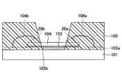
- the electrode pads 20a and 20b, the wiring patterns 102a and 102b, and the bonding wires 104a and 104b exposed on the surface of the humidity sensor 10A are sealed with a resin 105.
- a part of the moisture sensing portion (second moisture sensing film 19) of the humidity sensor 10 ⁇ / b> A is exposed without being sealed by the resin 105.
- water molecules can be quickly taken into the first moisture sensitive film 15 while protecting the electrode pads 20a, 20b, the wiring patterns 102a, 102b, and the bonding wires 104a, 104b from corrosion or the like.
- FIG. 11 is a diagram for explaining the humidity sensor 10A mounted on the mounting substrate, and shows the positional relationship between the humidity sensor 10A and the resin 105.
- FIG. 11 is a schematic cross-sectional view showing the positional relationship between the humidity sensor 10A and the resin 105.
- the lower view of FIG. 11 is a schematic plan view of the upper electrode 17.
- the resin 105 is formed on the second moisture-sensitive film 19 from the outermost peripheral edge of the upper electrode 17 to the outermost peripheral opening 17 a (the range indicated by a bidirectional arrow in the figure). ) Is a starting position and is preferably arranged toward the outer periphery of the humidity sensor 10A.
- the resin 105 is preferably provided so that the exposed portion of the second moisture sensitive film 19 is small while exposing all the openings 17a formed in the upper electrode 17. Thereby, the water droplet adhesion resistance is particularly improved.
- FIG. 12 is a schematic cross-sectional view showing a humidity sensor according to the second embodiment.
- the humidity sensor 10B includes the first moisture sensitive film 15 and the upper electrode 17 sandwiched between the lower electrode 13 and the upper electrode 17. And a second moisture sensitive film 19 to be covered.
- the area of the upper electrode 17 is larger than the area of the lower electrode 13 and smaller than the area of the first moisture sensitive film 15.
- the materials and thicknesses of the first moisture sensitive film 15 and the second moisture sensitive film 19 are the same as those of the humidity sensor 10A.
- the pattern of the conductor region of the upper electrode 17 and the opening 17a is the same as that of the humidity sensor 10A.
- the difference from the humidity sensor 10A according to the first embodiment is that the substrate 11 and the upper electrode 17 are electrically connected inside the humidity sensor 10B, and the potential of the upper electrode 17 is It is a fixed point.
- the upper electrode 17 has a p-type silicon substrate which is the substrate 11 through a p + layer which is a contact layer 31 formed on the surface of the p-type silicon substrate at a position where the opening 22 is formed. Electrically connected. Thereby, the potential of the upper electrode 17 is fixed to the same potential as that of the substrate 11.
- 13A to 13E, 14A to 14D, and 15A to 15C are process cross-sectional views for explaining the manufacturing method of the humidity sensor 10B according to the second embodiment.
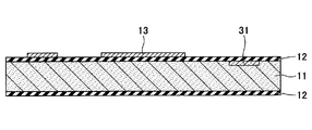
- a contact layer 31 is formed at a position where an electrode outlet of the upper electrode 17 is formed on the surface of the substrate 11.
- boron (B) is implanted by an ion implantation method (ion implantation method) into a position where an electrode outlet of the upper electrode 17 is formed on the surface of the silicon substrate, thereby forming a p + layer.
- annealing treatment may be performed as necessary. Note that a thermal diffusion method may be used instead of the ion implantation method.
- the insulating film 12 is formed on the substrate 11 as in the first embodiment.
- the lower electrode 13 is formed on the insulating film 12.
- the lower electrode may not be formed at the position where the contact layer 31 is formed.
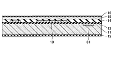
- a protective film 14 is formed so as to cover the lower electrode 13 as in the first embodiment.
- a first moisture sensitive film 15 is formed on the protective film 14 as in the first embodiment.
- a protective film 16 is formed on the first moisture sensitive film 15 as in the first embodiment.
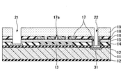
- a resist mask having an opening at a position corresponding to the electrode outlet is formed, and the insulating film 12, the protective film 14, and the first sensitivity are formed by reactive ion etching (RIE) or the like.
- RIE reactive ion etching
- the wet film 15 and the protective film 16 are partially removed. Thereby, a part of the lower electrode 13 and the contact layer 31 are exposed at predetermined positions.
- the upper electrode 17 is formed on the protective film 16 and the contact layer 31.
- the upper electrode 17 is electrically connected to the substrate 11 via the contact layer 31 at the electrode outlet, so that the upper electrode 17 and the substrate 11 are equipotential.
- it is possible to confine the electric field inside the first moisture sensitive film 15 and prevent water and dust from adhering to the humidity sensor 10B.
- heat treatment may be performed after the upper electrode 17 is formed.
- a protective film 18 is formed so as to cover the upper electrode 17.
- the second moisture sensitive film 19 is formed so as to cover the upper electrode 17 as in the first embodiment.
- electrode pads 20a and 20b are formed in the opening 21 and the opening 22 as in the first embodiment.
- backside polishing is performed as in the first embodiment.
- the humidity sensor 10B shown in FIG. 12 can be manufactured.
- Example 1 In Example 1, the characteristics of the substrate 11, the insulating film 12, the first moisture sensitive film 15, and the second moisture sensitive film 19 are fixed to the parameters shown below, and the area (outer shape) of the upper electrode 17 with respect to the lower electrode 13.
- the electrostatic capacitance value (arbitrary unit) when changing was calculated by simulation.
- the area of the first moisture sensitive film 15 was set to be larger than the area of the upper electrode 17. Further, the humidity sensor was operated by setting the potential of the substrate 11 during operation to a floating state, setting the lower electrode 13 to 1V and the upper electrode 17 to 0V.
- FIG. 16 is a diagram illustrating the effect of preventing the influence of water adhesion in the humidity sensor according to the first embodiment.
- the horizontal axis represents a value ( ⁇ m) obtained by subtracting the length of one side of the lower electrode 13 from the length of one side of the upper electrode 17. That is, it becomes 0 when the area of the upper electrode 17 and the area of the lower electrode 13 are equal, and becomes a positive value when the area of the upper electrode 17 is larger than the area of the lower electrode 13, and the area of the upper electrode 17 becomes lower. When the area is smaller than 13, the value is negative.
- the vertical axis indicates the capacitance value (arbitrary unit).
- a line A1 plotted with rhombus marks indicates a change in capacitance value when the first moisture sensitive film 15 is dried (humidity 0% Rh, relative dielectric constant 3.69).
- a line B1 plotted with square marks indicates a change in the capacitance value of the first moisture sensitive film 15 when the humidity is high (humidity 100% Rh, relative dielectric constant 4.19).
- a line C1 plotted with a triangular mark indicates a change in the capacitance value in a state where water is attached to the surface of the sensor (high humidity state + water attachment).
- FIG. 17 is a diagram illustrating the effect of preventing the influence of water adhesion in the humidity sensor according to the first embodiment.
- the horizontal axis indicates a value ( ⁇ m) obtained by subtracting the length of one side of the lower electrode 13 from the length of one side of the upper electrode 17 as in FIG.
- the vertical axis represents the difference in capacitance values (arbitrary unit).
- a line D1 plotted with square marks indicates a difference between the line C1 and the line B1.
- a line E1 indicated by a rhombus mark indicates a difference between the line B1 and the line A1.
- the line D1 which is the difference between the line C1 and the line B1 indicates a change in the capacitance value due to water adhesion, and the smaller this difference, the smaller the influence due to water adhesion.
- a line E1 that is a difference between the line B1 and the line A1 indicates a difference between the humid time and the dry time, and the larger the difference, the higher the sensitivity of the humidity sensor.
- Example 2 In Example 2, the simulation was performed under the same conditions as Example 1 except that the potential of the substrate 11 during operation was fixed (grounded) to 0V.
- FIG. 18 is a diagram illustrating the effect of preventing the influence of water adhesion in the humidity sensor according to the second embodiment.
- the horizontal axis represents a value ( ⁇ m) obtained by subtracting the length of one side of the lower electrode 13 from the length of one side of the upper electrode 17. That is, it becomes 0 when the area of the upper electrode 17 and the area of the lower electrode 13 are equal, and becomes a positive value when the area of the upper electrode 17 is larger than the area of the lower electrode 13, and the area of the upper electrode 17 becomes lower. When the area is smaller than 13, the value is negative.
- the vertical axis indicates the capacitance value (arbitrary unit).
- a line A2 plotted with rhombus marks indicates a change in the capacitance value when the first moisture sensitive film 15 is dried (humidity 0% Rh, relative dielectric constant 3.69).
- a line B2 plotted with square marks indicates a change in the capacitance value of the first moisture sensitive film 15 when the humidity is high (humidity 100% Rh, relative dielectric constant 4.19).
- a line C2 plotted with a triangle mark indicates a change in capacitance value in a state where water is attached to the surface of the sensor (high humidity state + water attachment).
- FIG. 19 is a diagram illustrating the effect of preventing the influence of water adhesion in the humidity sensor according to the second embodiment.
- the horizontal axis indicates the value ( ⁇ m) obtained by subtracting the length of one side of the lower electrode 13 from the length of one side of the upper electrode 17 as in FIG.
- the vertical axis represents the difference in capacitance values (arbitrary unit).
- a line D2 plotted with square marks indicates a difference between the line C2 and the line B2.
- a line E2 indicated by a rhombus mark indicates a difference between the line B2 and the line A2.
- the line D2 which is the difference between the line C2 and the line B2 indicates a change in the capacitance value due to water adhesion, and the smaller this difference, the smaller the influence due to water adhesion.
- a line E2 that is a difference between the line B2 and the line A2 indicates a difference between the humid time and the dry time, and the larger the difference, the higher the sensitivity of the humidity sensor.
- Example 2 in which the potential of the substrate 11 during operation is fixed (grounded) to 0 V, the influence of water adhesion is greatly reduced compared to Example 1 in which the potential of the substrate 11 during operation is in a floating state. I think it can be done. That is, it is preferable to fix the potential of the substrate 11 during operation to 0V.
- the area of the upper electrode 17 is made larger than the area of the lower electrode 13 and smaller than the area of the first moisture sensitive film 15, the influence on the sensor due to water adhesion is reduced and stable. It can be seen that the measured accuracy can be realized.
- the substrate 11 is a p-type silicon substrate
- the present invention is not limited to this, and the substrate 11 may be an n-type silicon substrate, for example.
- the upper electrode 17 and the substrate 11 are electrically connected as in the above embodiments.
- this embodiment is different from the above embodiments in that the potential of the lower electrode 13 is set to 0 V, and the potentials of the upper electrode 17 and the substrate 11 are driven with a positive potential larger than that of the lower electrode 13.
- the contact layer 31 is doped with a donor material such as phosphorus (P), antimony (Sb), arsenic (As), and the n + layer. May be formed.
Landscapes
- Chemical & Material Sciences (AREA)
- Chemical Kinetics & Catalysis (AREA)
- Electrochemistry (AREA)
- Physics & Mathematics (AREA)
- Health & Medical Sciences (AREA)
- Life Sciences & Earth Sciences (AREA)
- Analytical Chemistry (AREA)
- Biochemistry (AREA)
- General Health & Medical Sciences (AREA)
- General Physics & Mathematics (AREA)
- Immunology (AREA)
- Pathology (AREA)
- Engineering & Computer Science (AREA)
- Power Engineering (AREA)
- Investigating Or Analyzing Materials By The Use Of Electric Means (AREA)
Abstract
湿度センサは、基板の上に形成された下部電極と、前記下部電極を覆う第1の感湿膜と、前記第1の感湿膜の上に形成されて所定の開口パターンを有する上部電極と、前記上部電極を覆うと共に前記上部電極の開口部で前記第1の感湿膜に接続された第2の感湿膜と、を有し、前記上部電極の面積は、前記下部電極の面積よりも大きく、且つ前記第1の感湿膜の面積よりも小さい。
Description
本発明は湿度センサに関する。
湿度センサ、温度センサ、ガスセンサ、静電容量式タッチセンサ等、種々のセンサが産業用または個人向けの用途で多種多様な製品に用いられている。一般的に、センサの表面に水滴が付着するとセンサの動作に影響するため、結露や水滴に対する防御措置がとられている。
例えば、下部電極と上部電極の間に感湿膜を挟み込んだ平行平板型の湿度センサでは、保護膜で上部電極を覆う構成が知られている(例えば、特許文献1参照)。この文献では、保護膜と上部電極に、感湿膜を外界に露出させる開口部が形成され、開口部において、感湿膜は少なくとも保護膜の下面の位置よりも高い位置まで設けられている。
上部電極と下部電極の間に感湿膜を挟み込んだ平行平板型の湿度センサでは、上部電極の隙間から漏れ出る電界に水滴が付着すると、電気力線の状態が変化し、上部電極と下部電極の間に溜まる静電容量値が変化する。そのため、正確な湿度測定値を得ることができない。また、湿度センサの表面に付着した水滴中の塩類や不純成分が乾燥した後も残差として残り、感湿膜の特性が変化して安定したセンサ出力が得られない。
本発明は、上記の点に鑑みてなされてもので、湿度センサに対する水滴の影響を抑制し、精度良く安定した測定値を出力することのできる湿度センサを提供することを目的とする。
上記目的を達成するため、本発明の一態様に係る湿度センサ(10A,10B)は、基板(11)の上に形成された下部電極(13)と、前記下部電極(13)を覆う第1の感湿膜(15)と、前記第1の感湿膜(15)の上に形成されて所定の開口パターンを有する上部電極(17)と、前記上部電極(17)を覆うと共に前記上部電極(17)の開口部(17a)で前記第1の感湿膜(15)に接続された第2の感湿膜(19)と、を有し、前記上部電極(17)の面積は、前記下部電極(13)の面積よりも大きく、且つ前記第1の感湿膜(15)の面積よりも小さい。
なお、上記括弧内の参照符号は、理解を容易にするために付したものであり、一例にすぎず、図示の態様に限定されるものではない。
開示の湿度センサによれば、湿度センサに対する水滴の影響を防止し、精度良く安定した測定値を出力することができる。
以下、図面を参照して発明を実施するための形態について説明する。各図面において、同一構成部分には同一符号を付し、重複した説明を省略する場合がある。
最初に、湿度センサの原理について説明する。図1及び図2は、湿度センサの原理を説明するための図である。
図1に示されるように、平行平板型の湿度センサは、下部電極(BE)と上部電極(TE)の間に感湿膜を挟み込んだ構造を有する。湿度によって感湿膜に吸着する水分子の数が異なり、感湿膜の誘電率が変化する。感湿膜と水の比誘電率の差を利用して静電容量値の変化を捉える。
図2に示されるように、0%と100%の間で相対湿度(Rh)の変化に対応する静電容量値Cの変化を測定する。複数の既知の相対湿度で静電容量値Cを測定して近似式を得る。図2の例では、湿度HはH=a*C+bで線形近似される。勾配aと切片bを補正定数として用いて、測定した静電容量値を相対湿度に換算することができる。
平行平板型の湿度センサでは、感湿膜に空気中の水分を効率良く取り込んで応答性を高めるために、上部電極(TE)に開口パターンが形成される場合がある。この場合、上部電極(TE)の開口部から電界が空気中に漏れ出る。上述したように、漏れ電界に結露や水滴が付着すると電気力線の状態が変化し、上部電極(TE)と下部電極(BE)の間の静電容量値が上昇する。そうすると、もとの近似式(補正定数)が使えなくなり、湿度センサとしての機能が損なわれる。
そこで、以下に示す本発明の実施形態では、平行平板型の湿度センサにおいて、上部電極と下部電極の間に配置される第1の感湿膜と、上部電極を覆う第2の感湿膜とが積層した構造を採用する。また、上部電極の面積が、下部電極の面積よりも大きく、且つ第1の感湿膜の面積よりも小さい構造を採用する。これにより、湿度センサに対する水滴の影響を防止し、精度良く安定した測定値を出力することができる。
〔第1実施形態〕
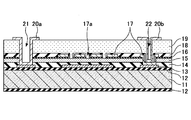
第1実施形態に係る湿度センサについて説明する。図3は、第1実施形態に係る湿度センサを示す概略断面図である。
第1実施形態に係る湿度センサについて説明する。図3は、第1実施形態に係る湿度センサを示す概略断面図である。
図3に示されるように、湿度センサ10Aは、基板11の上に、絶縁膜12、下部電極13、保護膜14、第1の感湿膜15、保護膜16、上部電極17、保護膜18、第2の感湿膜19、電極パッド20a,20bが積層された構造を有する。
基板11は、例えばシリコン基板等の半導体基板であってよく、絶縁性基板であってもよい。
絶縁膜12は、基板11の上に形成されている。絶縁膜12は、例えばシリコン酸化(SiO2)膜、シリコン窒化(SiN)膜であってよく、これらの積層膜であってもよい。なお、基板11として絶縁性基板を用いる場合には、絶縁膜12を設けなくてもよい。
下部電極13は、絶縁膜12の上に形成されている。下部電極13は、所定のパターンに形成されている。下部電極13は、例えばアルミニウム(Al)、Al-Si、Al-Si-Cuであってよく、金(Au)、白金(Pt)等の貴金属であってもよい。また、これらの下地膜としてニッケル(Ni)を形成してもよい。
保護膜14は、下部電極13を覆うように形成されている。保護膜14は、例えばSiO2膜、SiN膜であってよく、これらの積層膜であってもよい。保護膜14は、必須ではないが、下部電極13を腐食等から保護するという観点から、下部電極13を覆うように設けられていることが好ましい。なお、下部電極13として、Au、Pt等の貴金属を用いる場合には、保護膜14を設けなくてもよい。
第1の感湿膜15は、下部電極13と上部電極17との間に形成されている。第1の感湿膜15は、例えばポリイミド(PI)、セルロース、ポリメチルメタクリレート(PMMA)、ポリビニルアルコール(PVA)等の水分子を吸着しやすい高分子材料で形成されている。第1の感湿膜15の厚さは、短絡を防止するという観点から、0.5μm以上であることが好ましい。また、第1の感湿膜15の厚さは、応答性又は感度の観点から、1.5μm以下であることが好ましい。即ち、第1の感湿膜15の厚さは、0.5μm~1.5μmであることが好ましい。
上部電極17は、第1の感湿膜15の上に形成されている。上部電極17は、その面積が下部電極13の面積よりも大きくなるように、所定のパターンに形成されている。上部電極17は、例えば下部電極13と同様の材料により形成されていてよい。上部電極17は、所定の開口部17aを有し、開口部17a内で第1の感湿膜15と第2の感湿膜19とが連通している。開口部17aの大きさは、特性やプロセスを考慮して最適な設計値とされるが、開口部17aが小さいほど漏れ電界の閉じ込め効果を十分に発揮させることができるという観点から、可能な限り小さいほうが好ましい。
保護膜16,18は、上部電極17の全周を覆うように形成されている。これにより、耐水性が向上する。保護膜16,18は、例えばSiO2膜、SiN膜であってよく、これらの積層膜であってもよい。保護膜16,18は、必須ではないが、上部電極17を腐食等から保護するという観点から、上部電極17を覆うように設けられていることが好ましい。なお、上部電極17として、Au、Pt等の貴金属を使用した場合には、保護膜16,18を設けなくてもよい。
第2の感湿膜19は、上部電極17を覆うと共に、上部電極17の開口部17aで第1の感湿膜15に接続されるように形成されている。これにより、上部電極17の開口部17aから電界が漏れ出た場合でも、漏れ電界に水滴が接触することを防止できる。第2の感湿膜19は、第1の感湿膜15と同じ種類の膜であってもよく、異なる種類の膜であってもよいが、感湿特性の観点から、第1の感湿膜15と同じ種類の膜であることが好ましい。第2の感湿膜19の厚さは、漏れ電界への水滴の接触を効果的に防止するという観点から、第1の感湿膜15の厚さ以上であることが好ましい。また、第2の感湿膜19の厚さは、第1の感湿膜15へ迅速に水分子を取り込むという観点から、第1の感湿膜15の厚さの10倍以下であることが好ましい。即ち、第2の感湿膜19の厚さは、第1の感湿膜15の厚さの1~10倍であることが好ましい。
電極パッド20a,20bは、ワイヤボンディング用のパッドである。電極パッド20aは、下部電極13に到達する電極取り出し用の開口21に形成されている。電極パッド20bは、上部電極17に到達する電極取り出し用の開口22に形成されている。これにより、電極パッド20a,20bは、それぞれ下部電極13及び上部電極17と電気的に接続される。開口21及び開口22の大きさは、例えば40μm~120μm程度である。電極パッド20a,20bを介して下部電極13と上部電極17との間に所定の電圧を印加して、静電容量値Cを測定し、予め取得した近似式(補正定数)を用いて相対湿度を算出する。図3の構成では、上部電極17が漏れ電界の閉じ込め効果を有し、且つ第2の感湿膜19によってセンサ主要部が水分子の付着から保護されているので、測定された静電容量値から相対湿度への換算が正確に行われる。
図4は、第1実施形態に係る湿度センサ10Aの電極パターンの一例を示す図である。図4では、説明の便宜上、下部電極13、第1の感湿膜15及び上部電極17のみを図示し、その他の構成については図示を省略している。
図4の上部電極17のパターンは、下部電極13上の第1の感湿膜15上に形成される格子状のパターンであり、開口部17aを有する。図4では説明の便宜上、第2の感湿膜19の図示を省略しているが、上部電極17上に第2の感湿膜19が配置されるので、開口部17aからの漏れ電界への水滴の接触は抑制される。同時に、開口部17aから第1の感湿膜15へ最短パスで空気中の水分子を取り込むことができる。格子状の電極パターンを定義するライン・アンド・スペース(L/S)は、例えば1μm/1μm、2μm/2μm、5μm/5μm、10μm/10μmとすることができる。
また、上部電極17の面積は、下部電極13の面積よりも大きく、且つ第1の感湿膜15の面積よりも小さい。これにより、湿度センサに対する水滴の影響を防止し、精度良く安定した測定値を出力することができる。詳細については後述の実施例を用いて説明する。なお、下部電極13の面積とは、取り出し配線部を含まない部分の面積を意味し、上部電極17の面積とは、開口部17aを含み、取り出し配線部を含まない部分の面積を意味する。また、図4における一点鎖線A-Aの位置において切断した断面が、前述した図3に示される湿度センサ10Aの断面に対応する。
図5は、第1実施形態に係る湿度センサの電極パターンの別の例を示す図である。図5では、説明の便宜上、下部電極13、第1の感湿膜15及び上部電極17のみを図示し、その他の構成については図示を省略している。
図5の上部電極17のパターンは、下部電極13上の第1の感湿膜15上に形成されるラダー状のパターンであり、一方向に延びる開口部17bを有する。図5では説明の便宜上、第2の感湿膜19の図示を省略しているが、上部電極17上に第2の感湿膜19が配置されるので、開口部17bからの漏れ電界への水滴の接触は抑制される。同時に、開口部17bから第1の感湿膜15へ最短パスで空気中の水分子を取り込むことができる。ラダー状の電極パターンを定義するライン・アンド・スペース(L/S)は、例えば1μm/1μm、2μm/2μm、5μm/5μm、10μm/10μmとすることができる。
また、上部電極17の面積は、下部電極13の面積よりも大きく、且つ第1の感湿膜15の面積よりも小さい。これにより、湿度センサに対する水滴の影響を防止し、精度良く安定した測定値を出力することができる。詳細については後述の実施例を用いて説明する。
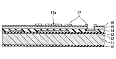
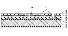
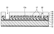
次に、図3及び図4の湿度センサ10Aの製造方法について説明する。図6A~D、図7A~D及び図8A~Cは、第1実施形態に係る湿度センサ10Aの製造方法を説明するための工程断面図である。
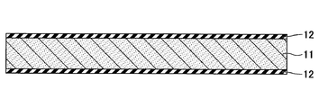
最初に、図6Aに示されるように、基板11の表面及び裏面に絶縁膜12を形成する。具体的には、p型のシリコン基板の表面及び裏面に、熱酸化により、例えば厚さが0.5μm~5μmのSiO2膜を形成する。なお、基板11の表面のみに、スパッタ等により、絶縁膜12を成膜してもよい。ここで、基板11の表面とは膜を積層する側の面(図中の上面)を意味する。
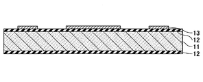
続いて、図6Bに示されるように、絶縁膜12の上に下部電極13を形成する。具体的には、SiO2膜の上に、例えば厚さが0.2μmのAl、Al-Si、Al-Si-Cu、Au、Pt等の電極材料を成膜し、フォトリソグラフィにより所望のパターンにパターニングする。
続いて、図6Cに示されるように、下部電極13を覆うように保護膜14を形成する。具体的には、下部電極13を覆うように、SiO2膜、SiN膜、これらの積層膜等の絶縁膜を成膜する。なお、下部電極13の電極材料として、Au、Pt等の貴金属を用いる場合には、保護膜14を形成しなくてもよい。
続いて、図6Dに示されるように、保護膜14の上に第1の感湿膜15を形成する。具体的には、保護膜14の上に、スピンコート、ディップ、コータ等により、PI、セルロース、PMMA、PVA等の水分子を吸着しやすい高分子材料を0.5μm~1.5μmの厚さに塗布する。
続いて、図7Aに示されるように、第1の感湿膜15の上に、保護膜16を形成する。具体的には、第1の感湿膜15の上に、SiO2膜、SiN膜、これらの積層膜等の絶縁膜を成膜する。なお、上部電極17の電極材料として、Au、Pt等の貴金属を用いる場合には、保護膜16を形成しなくてもよい。
続いて、図7Bに示されるように、電極取出口に対応する位置に開口を有するレジストマスクを形成し、反応性イオンエッチング(RIE)等により、保護膜14、第1の感湿膜15、及び保護膜16を部分的に除去する。これにより、下部電極13の一部を所定の箇所で露出させる。
続いて、図7Cに示されるように、保護膜16の上に上部電極17を形成する。具体的には、保護膜16の上に、例えば厚さが0.2μmのAl、Al-Si、Al-Si-Cu、Au、Pt等の電極材料を成膜し、フォトリソグラフィにより所望のパターンにパターニングする。このとき、上部電極17の面積が、下部電極13の面積よりも大きく、且つ第1の感湿膜15の面積よりも小さくなるようにパターニングする。なお、上部電極17を形成する前に、前処理(例えば、プラズマ等の表面改質処理)を行い、密着性を向上させてもよい。
続いて、図7Dに示されるように、上部電極17を覆うように保護膜18を形成する。具体的には、上部電極17を覆うように、SiO2膜、SiN膜、これらの積層膜等の絶縁膜を成膜し、開口部17a及び電極取出口に対応する位置に開口を有するレジストマスクを形成し、RIE等により、保護膜16,18を部分的に除去する。これにより、第1の感湿膜15及び上部電極17の一部を所定の箇所で露出させる。なお、上部電極17の電極材料として、Au、Pt等の貴金属を用いる場合には、保護膜18を形成しなくてもよい。
続いて、図8Aに示されるように、上部電極17を覆うように第2の感湿膜19を形成する。具体的には、保護膜18の上に、スピンコート、ディップ、コータ等により、PI、セルロース、PMMA、PVA等の水分子を吸着しやすい高分子材料を0.5μm~10μmの厚さに塗布する。このとき、上部電極17の開口部17aは第2の感湿膜19で埋め込まれる。その後、電極取出口に対応する位置に開口を有するレジストマスクを形成し、RIE等により、第2の感湿膜19を部分的に除去して下部電極13及び上部電極17の一部を所定の箇所で露出させる。これにより、下部電極13に到達する電極取り出し用の開口21、及び上部電極17に到達する電極取り出し用の開口22が形成される。
続いて、図8Bに示されるように、開口21及び開口22に、電極パッド20a,20bを形成する。具体的には、リフトオフにより、開口21及び開口22に厚さが0.5μm~0.6μmの金属膜を成膜する。
続いて、図8Cに示されるように、バックグラインド(裏面研磨)を行う。具体的には、p型のシリコン基板の裏面に形成されたSiO2膜及びp型のシリコン基板を研磨することにより、p型のシリコン基板を所望の厚さまで薄くする。
以上の工程により、図3及び図4に示される湿度センサ10Aを製造することができる。なお、図5に示される湿度センサについても、図3及び図4に示される湿度センサ10Aと同様の方法により製造することができる。
次に、第1実施形態に係る湿度センサ10Aを実装基板に搭載した構造について説明する。図9は、実装基板に搭載された湿度センサ10Aを説明するための図である。
図9に示されるように、湿度センサ10Aは、実装基板101上に形成された配線パターン102bの上に、銀ペースト等の導電性接着剤103を使用してダイボンディングされる。これにより、湿度センサ10Aの基板11と配線パターン102bとが電気的に接続される。また、湿度センサ10Aの上部電極17は、電極パッド20b及びボンディングワイヤ104bを介して配線パターン102bと電気的に接続されている。即ち、上部電極17は、湿度センサ10Aの外部に設けられたボンディングワイヤ104b及び配線パターン102bを介して基板11と電気的に接続されている。これにより、上部電極17と基板11とが等電位となる。その結果、電界を第1の感湿膜15の内部に閉じ込めて、湿度センサ10Aに水やゴミが付着することを抑制することができる。一方、下部電極13は、電極パッド20a及びボンディングワイヤ104aを介して配線パターン102aと電気的に接続されている。
なお、図9に示す例では、ボンディングワイヤ104b及び配線パターン102bを介して上部電極17と基板11とが電気的に接続される形態を示したが、上部電極17と基板11とを電気的に接続する方法はこれに限定されない。例えば、実装段階では、基板11と導通可能なように実装基板101側に取り出し配線を形成しておき、最終的な組み込み基板上で、上部電極17と基板11とが電気的に接続されるようにしてもよい。
次に、図9に示される実装基板に搭載された湿度センサ10Aを樹脂により封止した構造について説明する。
図10は、実装基板に搭載された湿度センサ10Aを説明するための図である。図10に示される構造では、湿度センサ10Aの表面に露出する電極パッド20a,20b、配線パターン102a,102b、及びボンディングワイヤ104a,104bが樹脂105により封止されている。一方、湿度センサ10Aの感湿部(第2の感湿膜19)の一部は、樹脂105により封止されることなく露出している。これにより、電極パッド20a,20b、配線パターン102a,102b、及びボンディングワイヤ104a,104bを、腐食等から保護しつつ、第1の感湿膜15へ迅速に水分子を取り込むことができる。
図11は、実装基板に搭載された湿度センサ10Aを説明するための図であり、湿度センサ10Aと樹脂105との位置関係を示している。図11の上図は、湿度センサ10Aと樹脂105との位置関係を示す概略断面図である。図11の下図は、上部電極17の概略平面図である。図11に示されるように、樹脂105は、第2の感湿膜19の上に、上部電極17の最外周縁から最外周の開口部17aまでの間(図中、双方向矢印で示す範囲)を開始位置とし、湿度センサ10Aの外周に向かって配置されていることが好ましい。言い換えると、樹脂105は、上部電極17に形成された全ての開口部17aを露出させつつ、第2の感湿膜19の露出部が小さくなるように設けられていることが好ましい。これにより、水滴付着耐性が特に向上する。
〔第2実施形態〕
第2実施形態に係る湿度センサについて説明する。図12は、第2実施形態に係る湿度センサを示す概略断面図である。
第2実施形態に係る湿度センサについて説明する。図12は、第2実施形態に係る湿度センサを示す概略断面図である。
第2実施形態に係る湿度センサ10Bは、第1実施形態に係る湿度センサ10Aと同様に、下部電極13と上部電極17との間に挟まれる第1の感湿膜15と、上部電極17を覆う第2の感湿膜19とを有する。また、上部電極17の面積は、下部電極13の面積よりも大きく、且つ第1の感湿膜15の面積よりも小さい。第1の感湿膜15と第2の感湿膜19の材料、厚さ等は、湿度センサ10Aと同様である。上部電極17の導体領域と開口部17aのパターンも湿度センサ10Aと同様である。
図12に示されるように、第1実施形態に係る湿度センサ10Aと異なる点は、基板11と上部電極17とが湿度センサ10Bの内部で電気的に接続されており、上部電極17の電位が固定されている点である。具体的には、上部電極17が、開口22が形成された位置において、p型のシリコン基板の表面に形成されたコンタクト層31であるp+層を介して基板11であるp型のシリコン基板と電気的に接続されている。これにより、上部電極17の電位が基板11と等しい電位に固定されている。
次に、図12の湿度センサ10Bの製造方法について説明する。図13A~E、図14A~D及び図15A~Cは、第2実施形態に係る湿度センサ10Bの製造方法を説明するための工程断面図である。
最初に、図13Aに示されるように、基板11の表面における上部電極17の電極取出口を形成する位置にコンタクト層31を形成する。具体的には、シリコン基板の表面における上部電極17の電極取出口を形成する位置に、イオンインプランテーション法(イオン注入法)によりボロン(B)を注入することで、p+層を形成する。また、注入したボロンを活性化させるために、必要に応じてアニール処理を行ってもよい。なお、イオン注入法に代えて、熱拡散法を用いてもよい。
続いて、図13Bに示されるように、第1実施形態と同様に、基板11の上に絶縁膜12を形成する。
続いて、図13Cに示されるように、絶縁膜12の上に下部電極13を形成する。このとき、第1実施形態と異なり、コンタクト層31を形成した位置には、下部電極を形成しなくてもよい。
続いて、図13Dに示されるように、第1実施形態と同様に、下部電極13を覆うように保護膜14を形成する。
続いて、図13Eに示されるように、第1実施形態と同様に、保護膜14の上に第1の感湿膜15を形成する。
続いて、図14Aに示されるように、第1実施形態と同様に、第1の感湿膜15の上に、保護膜16を形成する。
続いて、図14Bに示されるように、電極取出口に対応する位置に開口を有するレジストマスクを形成し、反応性イオンエッチング(RIE)等により、絶縁膜12、保護膜14、第1の感湿膜15、及び保護膜16を部分的に除去する。これにより、下部電極13の一部及びコンタクト層31を所定の箇所で露出させる。
続いて、図14Cに示されるように、保護膜16及びコンタクト層31の上に上部電極17を形成する。これにより、上部電極17は、電極取出口において、コンタクト層31を介して基板11と電気的に接続されるので、上部電極17と基板11とが等電位となる。その結果、電界を第1の感湿膜15の内部に閉じ込めて、湿度センサ10Bに水やゴミが付着することを抑制することができる。なお、コンタクト層31と上部電極17との間でオーミックコンタクト(接触)をとるために、上部電極17を形成した後に、熱処理(シンター)を行ってもよい。
続いて、図14Dに示されるように、第1実施形態と同様に、上部電極17を覆うように保護膜18を形成する。
続いて、図15Aに示されるように、第1実施形態と同様に、上部電極17を覆うように第2の感湿膜19を形成する。
続いて、図15Bに示されるように、第1実施形態と同様に、開口21及び開口22に、電極パッド20a,20bを形成する。
続いて、図15Cに示されるように、第1実施形態と同様に、裏面研磨を行う。
以上の工程により、図12に示される湿度センサ10Bを製造することができる。
本発明の実施形態に係る湿度センサの効果を確認するためのシミュレーション結果について、以下の実施例1及び実施例2により説明する。
〔実施例1〕
実施例1では、基板11、絶縁膜12、第1の感湿膜15及び第2の感湿膜19の特性を以下に示すパラメータに固定し、下部電極13に対する上部電極17の面積(外形)を変化させたときの静電容量値(arbitrary unit)をシミュレーションにより算出した。なお、第1の感湿膜15の面積は、上部電極17の面積よりも大きくなるように設定した。また、動作時の基板11の電位を浮遊(Float)状態とし、下部電極13を1V、上部電極17を0Vとして湿度センサを動作させた。
実施例1では、基板11、絶縁膜12、第1の感湿膜15及び第2の感湿膜19の特性を以下に示すパラメータに固定し、下部電極13に対する上部電極17の面積(外形)を変化させたときの静電容量値(arbitrary unit)をシミュレーションにより算出した。なお、第1の感湿膜15の面積は、上部電極17の面積よりも大きくなるように設定した。また、動作時の基板11の電位を浮遊(Float)状態とし、下部電極13を1V、上部電極17を0Vとして湿度センサを動作させた。
(パラメータ)
基板11 シリコン基板
絶縁膜12 SiO2膜(膜厚:5μm、比誘電率3.9)
第1の感湿膜15 PI膜(膜厚:1μm、0%Rh相当時の比誘電率:3.69、100%Rh相当時の比誘電率:4.19)
第2の感湿膜19 PI膜(膜厚:2μm、0%Rh相当時の比誘電率:3.69、100%Rh相当時の比誘電率:4.19)
基板11 シリコン基板
絶縁膜12 SiO2膜(膜厚:5μm、比誘電率3.9)
第1の感湿膜15 PI膜(膜厚:1μm、0%Rh相当時の比誘電率:3.69、100%Rh相当時の比誘電率:4.19)
第2の感湿膜19 PI膜(膜厚:2μm、0%Rh相当時の比誘電率:3.69、100%Rh相当時の比誘電率:4.19)
図16は、実施例1に係る湿度センサにおける水付着の影響の防止効果を示す図である。図中、横軸は上部電極17の1辺の長さから下部電極13の1辺の長さを引いた値(μm)を示す。即ち、上部電極17の面積と下部電極13の面積とが等しい場合に0となり、上部電極17の面積が下部電極13の面積よりも大きい場合に正の値となり、上部電極17の面積が下部電極13の面積よりも小さい場合に負の値となる。また、図中、縦軸は静電容量値(arbitrary unit)を示す。また、図中、菱形マークでプロットされたラインA1は、第1の感湿膜15の乾燥時(湿度0%Rh、比誘電率3.69)の静電容量値の変化を示す。四角マークでプロットされたラインB1は、第1の感湿膜15の多湿時(湿度100%Rh、比誘電率4.19)の静電容量値の変化を示す。三角マークでプロットされたラインC1は、センサの表面に水が付着した状態(多湿状態+水付着)での静電容量値の変化を示す。
図17は、実施例1に係る湿度センサにおける水付着の影響の防止効果を示す図である。図中、横軸は図16と同様に上部電極17の1辺の長さから下部電極13の1辺の長さを引いた値(μm)を示す。また、図中、縦軸は静電容量値の差(arbitrary unit)を示す。また、図中、四角マークでプロットされたラインD1は、ラインC1とラインB1との差を示す。菱形マークで示されるラインE1は、ラインB1とラインA1との差を示す。なお、ラインC1とラインB1との差であるラインD1は、水付着による静電容量値の変化を示すものであり、この差が小さいほど水付着による影響が小さいことを意味する。また、ラインB1とラインA1との差であるラインE1は、多湿時と乾燥時との差を示すものであり、この差が大きいほど湿度センサの感度が高いことを意味する。
図17に示されるように、上部電極17の長さを下部電極13の長さよりも長くした場合、上部電極17の長さが下部電極13の長さよりも短い場合と比較して、ラインD1で示される静電容量値の差が小さくなっていることが分かる。このことから、上部電極17の面積を下部電極13の面積よりも大きくすることで、水付着による影響を低減することができると考えられる。
また、図17に示されるように、下部電極13の長さに対する上部電極17の長さを変化させても、ラインE1で示される静電容量値の差はほとんど変化していない。このことから、上部電極17の長さを下部電極13の長さよりも長くした場合であっても、上部電極17の長さが下部電極13の長さと等しい場合や短い場合と同等の感度が得られると考えられる。
〔実施例2〕
実施例2では、動作時の基板11の電位を0Vに固定(接地)した点以外は、実施例1と同様の条件でシミュレーションを行った。
実施例2では、動作時の基板11の電位を0Vに固定(接地)した点以外は、実施例1と同様の条件でシミュレーションを行った。
図18は、実施例2に係る湿度センサにおける水付着の影響の防止効果を示す図である。図中、横軸は上部電極17の1辺の長さから下部電極13の1辺の長さを引いた値(μm)を示す。即ち、上部電極17の面積と下部電極13の面積とが等しい場合に0となり、上部電極17の面積が下部電極13の面積よりも大きい場合に正の値となり、上部電極17の面積が下部電極13の面積よりも小さい場合に負の値となる。また、図中、縦軸は静電容量値(arbitrary unit)を示す。また、図中、菱形マークでプロットされたラインA2は、第1の感湿膜15の乾燥時(湿度0%Rh、比誘電率3.69)の静電容量値の変化を示す。四角マークでプロットされたラインB2は、第1の感湿膜15の多湿時(湿度100%Rh、比誘電率4.19)の静電容量値の変化を示す。三角マークでプロットされたラインC2は、センサの表面に水が付着した状態(多湿状態+水付着)での静電容量値の変化を示す。
図19は、実施例2に係る湿度センサにおける水付着の影響の防止効果を示す図である。図中、横軸は図18と同様に上部電極17の1辺の長さから下部電極13の1辺の長さを引いた値(μm)を示す。また、図中、縦軸は静電容量値の差(arbitrary unit)を示す。また、図中、四角マークでプロットされたラインD2は、ラインC2とラインB2との差を示す。菱形マークで示されるラインE2は、ラインB2とラインA2との差を示す。なお、ラインC2とラインB2との差であるラインD2は、水付着による静電容量値の変化を示すものであり、この差が小さいほど水付着による影響が小さいことを意味する。また、ラインB2とラインA2との差であるラインE2は、多湿時と乾燥時との差を示すものであり、この差が大きいほど湿度センサの感度が高いことを意味する。
図19に示されるように、上部電極17の長さを下部電極13の長さよりも長くした場合、上部電極17の長さが下部電極13の長さよりも短い場合と比較して、ラインD2で示される静電容量値の差が小さくなっていることが分かる。このことから、上部電極17の面積を下部電極13の面積よりも大きくすることで、水付着による影響を低減することができると考えられる。
また、図19に示されるように、下部電極13の長さに対する上部電極17の長さを変化させても、ラインE2で示される静電容量値の差はほとんど変化していない。このことから、上部電極17の長さを下部電極13の長さよりも長くした場合であっても、上部電極17の長さが下部電極13の長さと等しい場合や短い場合と同等の感度が得られると考えられる。
さらに、動作時の基板11の電位を0Vに固定(接地)した実施例2では、動作時の基板11の電位を浮遊状態とした実施例1と比較して、水付着による影響を大幅に低減することができると考えられる。即ち、動作時の基板11の電位を0Vに固定することが好ましい。
このように、上部電極17の面積が、下部電極13の面積よりも大きく、且つ第1の感湿膜15の面積よりも小さくすることで、水付着によるセンサへの影響を低減して、安定した測定精度を実現できることが分かる。
以上、好ましい実施の形態について説明したが、上述した実施の形態に制限されることはなく、特許請求の範囲に記載された範囲を逸脱することなく、上述した実施の形態に種々の変形及び置換を加えることができる。
上記の各実施形態では、基板11がp型のシリコン基板である場合を例に挙げて説明したが、これに限定されず、例えば基板11はn型のシリコン基板であってもよい。この場合においても、上記の各実施形態と同様に、上部電極17と基板11とは電気的に接続されていることが好ましい。ただし、下部電極13の電位を0Vとし、上部電極17及び基板11の電位を下部電極13よりも大きい正の電位で駆動させる点で、上記の各実施形態とは異なる。また、第2実施形態において基板11をn型のシリコン基板とする場合には、コンタクト層31として、リン(P)、アンチモン(Sb)、ヒ素(As)等のドナー材料をドーピングしてn+層を形成すればよい。
本国際出願は、2017年3月31日に出願した日本国特許出願第2017-071469号に基づく優先権を主張するものであり、当該出願の全内容を本国際出願に援用する。
10A,10B 湿度センサ
11 基板
13 下部電極
15 第1の感湿膜
17 上部電極
17a 開口部
19 第2の感湿膜
22 開口
11 基板
13 下部電極
15 第1の感湿膜
17 上部電極
17a 開口部
19 第2の感湿膜
22 開口
Claims (9)
- 基板の上に形成された下部電極と、
前記下部電極を覆う第1の感湿膜と、
前記第1の感湿膜の上に形成されて所定の開口パターンを有する上部電極と、
前記上部電極を覆うと共に前記上部電極の開口部で前記第1の感湿膜に接続された第2の感湿膜と、
を有し、
前記上部電極の面積は、前記下部電極の面積よりも大きく、且つ前記第1の感湿膜の面積よりも小さい、
湿度センサ。 - 前記上部電極は、前記基板と電気的に接続されていることを特徴とする請求項1に記載の湿度センサ。
- 前記第1の感湿膜には、開口が形成されており、
前記上部電極は、前記開口を介して前記基板と電気的に接続されていることを特徴とする請求項2に記載の湿度センサ。 - 前記上部電極は、当該湿度センサの外部で前記基板と電気的に接続されていることを特徴とする請求項2に記載の湿度センサ。
- 前記基板は、動作時に電位が固定されることを特徴とする請求項1に記載の湿度センサ。
- 前記基板は、p型の半導体により形成されており、且つ接地されていることを特徴とする請求項5に記載の湿度センサ。
- 前記基板は、n型の半導体により形成されており、且つ正の電位に固定されていることを特徴とする請求項5に記載の湿度センサ。
- 前記上部電極の全周を覆う保護膜を有する、
請求項1に記載の湿度センサ。 - 前記第2の感湿膜の上に、前記上部電極の最外周縁から最外周の前記開口部までの間を開始位置とし、前記湿度センサの外周に向かって配置された樹脂を有する、
請求項1に記載の湿度センサ。
Priority Applications (2)
| Application Number | Priority Date | Filing Date | Title |
|---|---|---|---|
| US16/491,247 US11435310B2 (en) | 2017-03-31 | 2018-02-26 | Humidity sensor |
| CN201880019163.0A CN110494744B (zh) | 2017-03-31 | 2018-02-26 | 湿度传感器 |
Applications Claiming Priority (2)
| Application Number | Priority Date | Filing Date | Title |
|---|---|---|---|
| JP2017-071469 | 2017-03-31 | ||
| JP2017071469A JP6770238B2 (ja) | 2017-03-31 | 2017-03-31 | 湿度センサ |
Publications (1)
| Publication Number | Publication Date |
|---|---|
| WO2018180107A1 true WO2018180107A1 (ja) | 2018-10-04 |
Family
ID=63675309
Family Applications (1)
| Application Number | Title | Priority Date | Filing Date |
|---|---|---|---|
| PCT/JP2018/007053 Ceased WO2018180107A1 (ja) | 2017-03-31 | 2018-02-26 | 湿度センサ |
Country Status (4)
| Country | Link |
|---|---|
| US (1) | US11435310B2 (ja) |
| JP (1) | JP6770238B2 (ja) |
| CN (1) | CN110494744B (ja) |
| WO (1) | WO2018180107A1 (ja) |
Families Citing this family (5)
| Publication number | Priority date | Publication date | Assignee | Title |
|---|---|---|---|---|
| CN107668019A (zh) * | 2017-10-24 | 2018-02-09 | 好得科技(深圳)有限公司 | 一种智能侦测安全保护电捕鼠器 |
| JP7193203B2 (ja) * | 2018-11-16 | 2022-12-20 | ミネベアミツミ株式会社 | 検出装置 |
| US11313824B2 (en) * | 2018-11-16 | 2022-04-26 | Minebea Mitsumi Inc. | Detecting device |
| JP2021092453A (ja) * | 2019-12-11 | 2021-06-17 | ミネベアミツミ株式会社 | 湿度センサ |
| CN110927224B (zh) * | 2019-12-13 | 2021-07-23 | 潍坊歌尔微电子有限公司 | 基于聚酰亚胺的湿度传感器及其制备方法 |
Citations (8)
| Publication number | Priority date | Publication date | Assignee | Title |
|---|---|---|---|---|
| JPH01250850A (ja) * | 1988-03-31 | 1989-10-05 | Toshiba Corp | 半導体感湿素子 |
| JPH01277746A (ja) * | 1988-04-30 | 1989-11-08 | Toshiba Corp | 半導体センサ |
| JPH0210146A (ja) * | 1988-06-28 | 1990-01-12 | Nok Corp | 感湿素子およびその動作回路 |
| JPH0387642A (ja) * | 1989-08-11 | 1991-04-12 | Vaisala Oy | 容量性湿度センサの製造方法 |
| JPH04276544A (ja) * | 1991-03-05 | 1992-10-01 | Nikon Corp | 接合型化学センサ |
| JP2009516192A (ja) * | 2005-11-17 | 2009-04-16 | エヌエックスピー ビー ヴィ | 湿度センサー |
| JP2014062885A (ja) * | 2012-08-27 | 2014-04-10 | Denso Corp | センサパッケージおよびその製造方法 |
| US20150047430A1 (en) * | 2011-11-16 | 2015-02-19 | Tim Benzel | Integrated humidity sensor and method for the manufacture thereof |
Family Cites Families (25)
| Publication number | Priority date | Publication date | Assignee | Title |
|---|---|---|---|---|
| JPS5389058A (en) | 1977-01-07 | 1978-08-05 | Toshiba Corp | Refrigerating cycle |
| US4564882A (en) * | 1984-08-16 | 1986-01-14 | General Signal Corporation | Humidity sensing element |
| DE3751502T2 (de) * | 1986-03-11 | 1996-02-15 | Kanegafuchi Chemical Ind | Elektrische oder elektronische Anordnung mit einer dünnen Schicht aus Polyimid. |
| EP0311939A3 (en) * | 1987-10-12 | 1990-10-17 | Nihon Parkerizing Co., Ltd. | Humidity sensor |
| JPH0318750A (ja) * | 1989-06-15 | 1991-01-28 | Seiko Epson Corp | 湿度センサ素子 |
| JPH03163345A (ja) * | 1989-11-22 | 1991-07-15 | Yamatake Honeywell Co Ltd | 感湿素子 |
| DE19549146A1 (de) * | 1995-12-29 | 1997-07-03 | Siemens Ag | Gassensor |
| JP4348757B2 (ja) * | 1998-11-12 | 2009-10-21 | ソニー株式会社 | 半導体装置 |
| US20040194546A1 (en) * | 2001-08-31 | 2004-10-07 | Masashi Kanehori | Capacitive humidity-sensor and capacitive humidity-sensor manufacturing method |
| CN100476418C (zh) * | 2007-03-28 | 2009-04-08 | 哈尔滨理工大学 | 平板夹心结构的半导体式气体传感器的制造方法 |
| JP2011080833A (ja) * | 2009-10-06 | 2011-04-21 | Alps Electric Co Ltd | 湿度検出センサ |
| JP5470512B2 (ja) * | 2009-11-30 | 2014-04-16 | アルプス電気株式会社 | 湿度検出センサ |
| CN103154715B (zh) | 2010-10-04 | 2015-07-22 | 阿尔卑斯电气株式会社 | 湿度检测传感器及其制造方法 |
| JP5488534B2 (ja) * | 2011-06-06 | 2014-05-14 | 株式会社デンソー | 湿度センサ及びその製造方法 |
| CN105229463B (zh) * | 2013-05-30 | 2019-08-02 | 维萨拉公司 | 双气体传感器结构及测量方法 |
| WO2015022891A1 (ja) * | 2013-08-13 | 2015-02-19 | 株式会社村田製作所 | 温湿度センサ |
| CN103616087B (zh) * | 2013-10-28 | 2016-02-17 | 天津科技大学 | 一种冷藏运输载具用温湿度传感器及其制备方法 |
| CN103698365B (zh) * | 2013-12-31 | 2015-10-14 | 中国工程物理研究院化工材料研究所 | 一种气敏传感器制备方法 |
| JP6535185B2 (ja) * | 2015-03-04 | 2019-06-26 | エイブリック株式会社 | 湿度センサ |
| CN205067413U (zh) * | 2015-06-15 | 2016-03-02 | 兰州交通大学 | 一种快速响应孔状上电极和感湿膜平行板电容式湿敏元件 |
| CN104914139A (zh) * | 2015-06-15 | 2015-09-16 | 兰州交通大学 | 一种快速响应孔状上电极和感湿膜平行板电容式湿敏元件 |
| CN104931546A (zh) * | 2015-06-15 | 2015-09-23 | 兰州交通大学 | 一种微型快速响应孔状上电极平行板电容式湿敏元件 |
| CN205067412U (zh) * | 2015-06-15 | 2016-03-02 | 兰州交通大学 | 一种微型快速响应孔状上电极平行板电容式湿敏元件 |
| CN105675671A (zh) * | 2016-01-29 | 2016-06-15 | 陈杨珑 | 一种用于石油开采的地下管道 |
| CN106124574B (zh) * | 2016-06-16 | 2019-04-12 | 西南交通大学 | 氧化石墨烯量子点湿度传感器及其制备方法 |
-
2017
- 2017-03-31 JP JP2017071469A patent/JP6770238B2/ja not_active Expired - Fee Related
-
2018
- 2018-02-26 WO PCT/JP2018/007053 patent/WO2018180107A1/ja not_active Ceased
- 2018-02-26 US US16/491,247 patent/US11435310B2/en active Active
- 2018-02-26 CN CN201880019163.0A patent/CN110494744B/zh not_active Expired - Fee Related
Patent Citations (8)
| Publication number | Priority date | Publication date | Assignee | Title |
|---|---|---|---|---|
| JPH01250850A (ja) * | 1988-03-31 | 1989-10-05 | Toshiba Corp | 半導体感湿素子 |
| JPH01277746A (ja) * | 1988-04-30 | 1989-11-08 | Toshiba Corp | 半導体センサ |
| JPH0210146A (ja) * | 1988-06-28 | 1990-01-12 | Nok Corp | 感湿素子およびその動作回路 |
| JPH0387642A (ja) * | 1989-08-11 | 1991-04-12 | Vaisala Oy | 容量性湿度センサの製造方法 |
| JPH04276544A (ja) * | 1991-03-05 | 1992-10-01 | Nikon Corp | 接合型化学センサ |
| JP2009516192A (ja) * | 2005-11-17 | 2009-04-16 | エヌエックスピー ビー ヴィ | 湿度センサー |
| US20150047430A1 (en) * | 2011-11-16 | 2015-02-19 | Tim Benzel | Integrated humidity sensor and method for the manufacture thereof |
| JP2014062885A (ja) * | 2012-08-27 | 2014-04-10 | Denso Corp | センサパッケージおよびその製造方法 |
Also Published As
| Publication number | Publication date |
|---|---|
| JP6770238B2 (ja) | 2020-10-14 |
| CN110494744B (zh) | 2022-02-25 |
| CN110494744A (zh) | 2019-11-22 |
| US20200033285A1 (en) | 2020-01-30 |
| US11435310B2 (en) | 2022-09-06 |
| JP2018173335A (ja) | 2018-11-08 |
Similar Documents
| Publication | Publication Date | Title |
|---|---|---|
| JP6984104B2 (ja) | 湿度センサ | |
| JP5425214B2 (ja) | 静電容量型湿度センサおよびその製造方法 | |
| WO2018180107A1 (ja) | 湿度センサ | |
| JP4770530B2 (ja) | 容量式湿度センサ | |
| CN103748457A (zh) | 湿度传感器及其制造方法 | |
| KR101104306B1 (ko) | 온도 및 다중 가스 감응 센서 어레이 및 이의 제조방법 | |
| JP5470512B2 (ja) | 湿度検出センサ | |
| WO2012160806A1 (ja) | 容量式湿度センサ | |
| JP2018059716A (ja) | センサ装置 | |
| JP4674529B2 (ja) | 湿度センサ装置及びその製造方法 | |
| US20180100825A1 (en) | Sensor of volatile substances with integrated heater and process for manufacturing a sensor of volatile substances | |
| JP2011080833A (ja) | 湿度検出センサ | |
| JP2017219441A (ja) | Memsガスセンサ、memsガスセンサ実装体、memsガスセンサ・パッケージ、memsガスセンサ組立体、及びmemsガスセンサの製造方法 | |
| WO2011149331A1 (en) | Capacitive humidity sensor and method of fabricating thereof | |
| JP4219876B2 (ja) | 容量式湿度センサ及びその製造方法 | |
| CN106158743A (zh) | 利用多感应像素检测多种气体的传感器的制造方法 | |
| JP5849836B2 (ja) | 湿度センサ | |
| JP6611362B2 (ja) | 容量式湿度センサ | |
| JP2018059717A (ja) | センサ素子 | |
| KR20150014550A (ko) | 정전기력을 이용한 캔틸레버 습도센서 | |
| WO2019142593A1 (ja) | 湿度検知装置 | |
| WO2019142592A1 (ja) | 湿度検知装置 | |
| WO2019181771A1 (ja) | 湿度検知装置 | |
| JPH09331070A (ja) | 静電容量型物理量センサ |
Legal Events
| Date | Code | Title | Description |
|---|---|---|---|
| 121 | Ep: the epo has been informed by wipo that ep was designated in this application |
Ref document number: 18777021 Country of ref document: EP Kind code of ref document: A1 |
|
| NENP | Non-entry into the national phase |
Ref country code: DE |
|
| 122 | Ep: pct application non-entry in european phase |
Ref document number: 18777021 Country of ref document: EP Kind code of ref document: A1 |