WO2018179685A1 - 基板処理装置 - Google Patents
基板処理装置 Download PDFInfo
- Publication number
- WO2018179685A1 WO2018179685A1 PCT/JP2018/000912 JP2018000912W WO2018179685A1 WO 2018179685 A1 WO2018179685 A1 WO 2018179685A1 JP 2018000912 W JP2018000912 W JP 2018000912W WO 2018179685 A1 WO2018179685 A1 WO 2018179685A1
- Authority
- WO
- WIPO (PCT)
- Prior art keywords
- substrate
- polishing
- elastic film
- sensor
- processing apparatus
- Prior art date
Links
Images


Classifications
-
- B—PERFORMING OPERATIONS; TRANSPORTING
- B24—GRINDING; POLISHING
- B24B—MACHINES, DEVICES, OR PROCESSES FOR GRINDING OR POLISHING; DRESSING OR CONDITIONING OF ABRADING SURFACES; FEEDING OF GRINDING, POLISHING, OR LAPPING AGENTS
- B24B37/00—Lapping machines or devices; Accessories
- B24B37/27—Work carriers
- B24B37/30—Work carriers for single side lapping of plane surfaces
-
- B—PERFORMING OPERATIONS; TRANSPORTING
- B24—GRINDING; POLISHING
- B24B—MACHINES, DEVICES, OR PROCESSES FOR GRINDING OR POLISHING; DRESSING OR CONDITIONING OF ABRADING SURFACES; FEEDING OF GRINDING, POLISHING, OR LAPPING AGENTS
- B24B49/00—Measuring or gauging equipment for controlling the feed movement of the grinding tool or work; Arrangements of indicating or measuring equipment, e.g. for indicating the start of the grinding operation
- B24B49/10—Measuring or gauging equipment for controlling the feed movement of the grinding tool or work; Arrangements of indicating or measuring equipment, e.g. for indicating the start of the grinding operation involving electrical means
-
- H—ELECTRICITY
- H01—ELECTRIC ELEMENTS
- H01L—SEMICONDUCTOR DEVICES NOT COVERED BY CLASS H10
- H01L21/00—Processes or apparatus adapted for the manufacture or treatment of semiconductor or solid state devices or of parts thereof
- H01L21/02—Manufacture or treatment of semiconductor devices or of parts thereof
- H01L21/04—Manufacture or treatment of semiconductor devices or of parts thereof the devices having at least one potential-jump barrier or surface barrier, e.g. PN junction, depletion layer or carrier concentration layer
- H01L21/18—Manufacture or treatment of semiconductor devices or of parts thereof the devices having at least one potential-jump barrier or surface barrier, e.g. PN junction, depletion layer or carrier concentration layer the devices having semiconductor bodies comprising elements of Group IV of the Periodic System or AIIIBV compounds with or without impurities, e.g. doping materials
- H01L21/30—Treatment of semiconductor bodies using processes or apparatus not provided for in groups H01L21/20 - H01L21/26
- H01L21/302—Treatment of semiconductor bodies using processes or apparatus not provided for in groups H01L21/20 - H01L21/26 to change their surface-physical characteristics or shape, e.g. etching, polishing, cutting
- H01L21/304—Mechanical treatment, e.g. grinding, polishing, cutting
-
- H—ELECTRICITY
- H01—ELECTRIC ELEMENTS
- H01L—SEMICONDUCTOR DEVICES NOT COVERED BY CLASS H10
- H01L21/00—Processes or apparatus adapted for the manufacture or treatment of semiconductor or solid state devices or of parts thereof
- H01L21/02—Manufacture or treatment of semiconductor devices or of parts thereof
- H01L21/04—Manufacture or treatment of semiconductor devices or of parts thereof the devices having at least one potential-jump barrier or surface barrier, e.g. PN junction, depletion layer or carrier concentration layer
- H01L21/18—Manufacture or treatment of semiconductor devices or of parts thereof the devices having at least one potential-jump barrier or surface barrier, e.g. PN junction, depletion layer or carrier concentration layer the devices having semiconductor bodies comprising elements of Group IV of the Periodic System or AIIIBV compounds with or without impurities, e.g. doping materials
- H01L21/30—Treatment of semiconductor bodies using processes or apparatus not provided for in groups H01L21/20 - H01L21/26
- H01L21/302—Treatment of semiconductor bodies using processes or apparatus not provided for in groups H01L21/20 - H01L21/26 to change their surface-physical characteristics or shape, e.g. etching, polishing, cutting
- H01L21/306—Chemical or electrical treatment, e.g. electrolytic etching
- H01L21/30625—With simultaneous mechanical treatment, e.g. mechanico-chemical polishing
-
- H—ELECTRICITY
- H01—ELECTRIC ELEMENTS
- H01L—SEMICONDUCTOR DEVICES NOT COVERED BY CLASS H10
- H01L21/00—Processes or apparatus adapted for the manufacture or treatment of semiconductor or solid state devices or of parts thereof
- H01L21/67—Apparatus specially adapted for handling semiconductor or electric solid state devices during manufacture or treatment thereof; Apparatus specially adapted for handling wafers during manufacture or treatment of semiconductor or electric solid state devices or components ; Apparatus not specifically provided for elsewhere
- H01L21/67005—Apparatus not specifically provided for elsewhere
- H01L21/67011—Apparatus for manufacture or treatment
- H01L21/67092—Apparatus for mechanical treatment
-
- H—ELECTRICITY
- H01—ELECTRIC ELEMENTS
- H01L—SEMICONDUCTOR DEVICES NOT COVERED BY CLASS H10
- H01L21/00—Processes or apparatus adapted for the manufacture or treatment of semiconductor or solid state devices or of parts thereof
- H01L21/67—Apparatus specially adapted for handling semiconductor or electric solid state devices during manufacture or treatment thereof; Apparatus specially adapted for handling wafers during manufacture or treatment of semiconductor or electric solid state devices or components ; Apparatus not specifically provided for elsewhere
- H01L21/67005—Apparatus not specifically provided for elsewhere
- H01L21/67011—Apparatus for manufacture or treatment
- H01L21/67155—Apparatus for manufacturing or treating in a plurality of work-stations
- H01L21/67207—Apparatus for manufacturing or treating in a plurality of work-stations comprising a chamber adapted to a particular process
- H01L21/67219—Apparatus for manufacturing or treating in a plurality of work-stations comprising a chamber adapted to a particular process comprising at least one polishing chamber
-
- H—ELECTRICITY
- H01—ELECTRIC ELEMENTS
- H01L—SEMICONDUCTOR DEVICES NOT COVERED BY CLASS H10
- H01L21/00—Processes or apparatus adapted for the manufacture or treatment of semiconductor or solid state devices or of parts thereof
- H01L21/67—Apparatus specially adapted for handling semiconductor or electric solid state devices during manufacture or treatment thereof; Apparatus specially adapted for handling wafers during manufacture or treatment of semiconductor or electric solid state devices or components ; Apparatus not specifically provided for elsewhere
- H01L21/67005—Apparatus not specifically provided for elsewhere
- H01L21/67242—Apparatus for monitoring, sorting or marking
- H01L21/67259—Position monitoring, e.g. misposition detection or presence detection
-
- H—ELECTRICITY
- H01—ELECTRIC ELEMENTS
- H01L—SEMICONDUCTOR DEVICES NOT COVERED BY CLASS H10
- H01L21/00—Processes or apparatus adapted for the manufacture or treatment of semiconductor or solid state devices or of parts thereof
- H01L21/67—Apparatus specially adapted for handling semiconductor or electric solid state devices during manufacture or treatment thereof; Apparatus specially adapted for handling wafers during manufacture or treatment of semiconductor or electric solid state devices or components ; Apparatus not specifically provided for elsewhere
- H01L21/67005—Apparatus not specifically provided for elsewhere
- H01L21/67242—Apparatus for monitoring, sorting or marking
- H01L21/67294—Apparatus for monitoring, sorting or marking using identification means, e.g. labels on substrates or labels on containers
-
- H—ELECTRICITY
- H01—ELECTRIC ELEMENTS
- H01L—SEMICONDUCTOR DEVICES NOT COVERED BY CLASS H10
- H01L22/00—Testing or measuring during manufacture or treatment; Reliability measurements, i.e. testing of parts without further processing to modify the parts as such; Structural arrangements therefor
- H01L22/20—Sequence of activities consisting of a plurality of measurements, corrections, marking or sorting steps
- H01L22/26—Acting in response to an ongoing measurement without interruption of processing, e.g. endpoint detection, in-situ thickness measurement
-
- B—PERFORMING OPERATIONS; TRANSPORTING
- B23—MACHINE TOOLS; METAL-WORKING NOT OTHERWISE PROVIDED FOR
- B23Q—DETAILS, COMPONENTS, OR ACCESSORIES FOR MACHINE TOOLS, e.g. ARRANGEMENTS FOR COPYING OR CONTROLLING; MACHINE TOOLS IN GENERAL CHARACTERISED BY THE CONSTRUCTION OF PARTICULAR DETAILS OR COMPONENTS; COMBINATIONS OR ASSOCIATIONS OF METAL-WORKING MACHINES, NOT DIRECTED TO A PARTICULAR RESULT
- B23Q15/00—Automatic control or regulation of feed movement, cutting velocity or position of tool or work
- B23Q15/007—Automatic control or regulation of feed movement, cutting velocity or position of tool or work while the tool acts upon the workpiece
- B23Q15/16—Compensation for wear of the tool
Definitions
- the present invention relates to a substrate processing apparatus for processing the surface of a substrate such as a semiconductor wafer.
- substrate processing apparatuses such as a substrate polishing apparatus for polishing a substrate such as a semiconductor wafer and a substrate cleaning apparatus for cleaning a substrate surface
- consumables such as a polishing pad are used.
- a polishing apparatus is known in which an RF tag that records information on the type and characteristics of these consumables is attached to the consumables, and the information is read when the apparatus is used (see Patent Document 1).
- Japanese Patent Laid-Open No. 2004-228688 discloses a case where the memory information of the RF tag is erased when a consumable such as a polishing pad is removed from the apparatus to prevent information leakage, and when an abnormality is detected by the abnormality monitoring unit. Discloses a polishing apparatus in which abnormal information is written in an RF tag.
- the present invention has been made in view of the above, and provides a substrate processing apparatus capable of making substrate processing conditions constant by more accurately detecting the status of consumables used for substrate processing. With the goal.
- One aspect of the present invention is a substrate processing apparatus that processes a substrate, the consumable used in the substrate processing apparatus, and a physical quantity of the consumable that is attached to the consumable and measures the physical quantity.
- At least one sensor provided with a storage unit and a communication unit for storing; a detector provided in the vicinity of the consumables; and a sensor for reading and writing information between the sensors attached to the consumables; and the detector
- a control device that sets processing conditions in the substrate processing apparatus based on a physical quantity of the consumables connected and read from the sensor.
- identification information of the sensor is stored in the storage unit, and the consumable is attached to the control device based on the identification information read from the sensor. Further, it is preferable to determine whether or not the substrate processing apparatus can be driven. In addition, it is preferable that information regarding the processing conditions of the substrate is recorded in a storage unit in the sensor when an abnormality occurs in the substrate processing apparatus.
- a substrate processing apparatus is a substrate polishing apparatus comprising: a polishing pad for polishing the substrate; and a substrate holding unit for holding the substrate and pressing the substrate against the polishing pad.
- the consumable is an elastic film that is attached to the substrate holding unit and holds a surface opposite to the polishing surface of the substrate, and the sensor is a strain sensor that measures strain of the elastic film, and the control device Can set processing conditions in the substrate processing apparatus based on the strain information of the elastic film measured by the strain sensor.
- At least one pressure chamber is formed between the elastic film and the substrate holding unit, and the control device is based on strain information of the elastic film measured by the strain sensor.
- the pressure in the pressure chamber is preferably adjusted. Due to variations in production of elastic membranes and variations in physical properties of raw material lots, even if pressure is applied at the same internal pressure, the elastic membrane does not swell in the same way, and the pressure applied to the substrate may vary depending on the individual elastic membrane. This variation can be canceled by adjusting the pressure.
- the substrate polishing apparatus includes an injection unit for separating the polished substrate from the elastic film by injecting gas or liquid onto the side wall of the elastic film holding the substrate.
- the control device may adjust the pressure in the pressure chamber based on strain information of the elastic film so that gas or liquid from the injection unit is injected to a boundary between the elastic film and the substrate. preferable. Thereby, gas or liquid can be effectively injected to the boundary between the elastic film and the substrate.
- the jetting unit is capable of adjusting the jetting angle of the gas or liquid, and from the image obtained by the imaging unit that images the boundary portion between the elastic film and the substrate, An image processing unit for detecting a position of the boundary part; and an injection angle adjusting unit for determining an injection angle by the injection unit based on the position of the boundary part detected by the image processing unit and adjusting the injection angle; It is preferable to provide.
- a substrate processing apparatus is a substrate polishing apparatus comprising: a polishing pad for polishing the substrate; and a substrate holding unit for holding the substrate and pressing the substrate against the polishing pad.
- the consumable is a retainer ring that supports the outer periphery of the substrate
- the sensor is a plurality of strain sensors that measure the strain of the retainer ring
- the control device detects the amount of strain detected by the plurality of strain sensors. It is preferable to detect whether or not the variation of the difference is within a predetermined value.
- the shape of the grounding surface of the retainer ring does not follow the polishing surface of the polishing pad, resulting in variations in how the retainer ring contacts the polishing surface.
- the compressive force applied in the vertical direction of the retainer ring also varies depending on the position of the ring. For this reason, the amount of strain detected by a plurality of strain sensors provided in the retainer ring also varies, but when the break-in of the retainer ring is completed, the shape of the retainer ring grounding surface follows the polishing surface of the pad. The variation in the amount of distortion detected by the plurality of strain sensors is reduced. Thereby, it is possible to effectively detect that the break-in of the retainer ring has been completed.
- a substrate processing apparatus is a substrate polishing apparatus comprising: a polishing pad for polishing the substrate; and a substrate holding unit for holding the substrate and pressing the substrate against the polishing pad.
- the consumable is a retainer ring that supports the outer periphery of the substrate
- the sensor is a plurality of strain sensors that measure the strain of the retainer ring
- the control device detects the amount of strain detected by the plurality of strain sensors.
- the processing conditions of the substrate are changed in accordance with the distribution of.
- a sensor for measuring the physical quantity of a consumable used in the substrate processing apparatus is attached to the consumable, and the processing conditions in the substrate processing apparatus are determined based on the physical quantity of the consumable read out from the sensor. Since it is set, the status of the consumables used for the substrate processing can be detected more accurately, and the substrate processing conditions can be made constant.
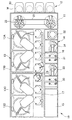
- FIG. 1 is a plan view showing the overall configuration of the substrate processing apparatus.
- the substrate processing apparatus 10 is divided into a load / unload unit 12, a polishing unit 13, and a cleaning unit 14, which are provided inside a rectangular housing 11.
- the substrate processing apparatus 10 also includes a control device 15 that controls operation of processing such as substrate transport, polishing, and cleaning.
- the load / unload unit 12 includes a plurality of front load units 20, a travel mechanism 21, and two transfer robots 22.
- a substrate cassette that stocks a large number of substrates (substrates) is placed on the front load unit 20.
- the transfer robot 22 has two hands up and down, and moves on the traveling mechanism 21 to take out the substrate W from the substrate cassette in the front load unit 20 and send it to the polishing unit 13, and from the cleaning unit 14. An operation of returning the processed substrate to be sent back to the substrate cassette is performed.
- the polishing unit 13 is an area for polishing (planarizing) the substrate, and is provided with a plurality of polishing units 13A to 13D, which are arranged along the longitudinal direction of the substrate processing apparatus.
- Each polishing unit includes a top ring for polishing the substrate W on the polishing table against the polishing pad, a polishing liquid supply nozzle for supplying a polishing liquid and a dressing liquid to the polishing pad, and a polishing surface of the polishing pad.
- a dresser that performs dressing and an atomizer that sprays a mixed fluid of liquid and gas or a mist-like liquid onto the polishing surface to wash away polishing debris and abrasive grains remaining on the polishing surface are provided.
- first and second linear transporters 16 and 17 are provided between the polishing unit 13 and the cleaning unit 14.
- the first linear transporter 16 has a first position for receiving the substrate W from the load / unload unit 12, second and third positions for transferring the substrate W between the polishing units 13A and 13B, and a second linear transporter. It is possible to move between a fourth position for delivering the substrate W to 17.
- the second linear transporter 17 is between the fifth position for receiving the substrate W from the first linear transporter 16 and the sixth and seventh positions for transferring the substrate W between the polishing units 13C and 13D. It is supposed to be movable.
- a swing transporter 23 for sending the substrate W to the cleaning unit 14 is provided between the transporters 16 and 17.
- the cleaning unit 14 includes a first substrate cleaning device 30, a second substrate cleaning device 31, a substrate drying device 32, and transfer robots 33 and 34 for transferring substrates between these devices.
- the substrate W that has been subjected to the polishing process by the polishing unit is cleaned (primary cleaning) by the first substrate cleaning device 30 and then further cleaned (finish cleaning) by the second substrate cleaning device 31.
- the cleaned substrate is transferred from the second substrate cleaning device 31 to the substrate drying device 32 and subjected to spin drying.
- the dried substrate W is returned to the load / unload unit 12.
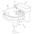
- FIG. 2 is a perspective view schematically showing the configuration of the polishing unit
- FIG. 3 is a side view schematically showing the configuration of the polishing unit.
- the polishing unit 40 holds a wafer (substrate) W and rotates it, a top ring (substrate holding device) 41, a polishing table 43 that instructs the polishing pad 42, and polishing that supplies slurry (polishing liquid) to the polishing pad 42.
- a liquid supply nozzle 45 and a film thickness sensor 47 that acquires a signal that changes according to the film thickness of the wafer W are provided.
- the top ring 41 is configured to hold the wafer W by vacuum suction on the lower surface thereof.
- the top ring 41 and the polishing table 43 rotate in the direction indicated by the arrow. In this state, the top ring 41 presses the wafer W against the upper polishing surface 42 a of the polishing pad 42. In the presence of the polishing liquid supplied from the polishing liquid supply nozzle 45 onto the polishing pad 42, the wafer W is slid in contact with the polishing pad 42 and polished.
- the film thickness sensor 47 is, for example, an optical sensor or an eddy current sensor, and is installed inside the polishing table 43. During polishing of the wafer W, the film thickness sensor 47 rotates with the polishing table 43 and acquires a film thickness signal corresponding to the film thickness when crossing the surface of the wafer W. The film thickness signal from the film thickness sensor 47 is transmitted to the control device 15, and the film thickness device 15 ends the polishing of the wafer W when the film thickness of the wafer W indicated by the film thickness signal reaches a set value.
- the top ring 41 includes a head main body 48 that presses the wafer W against the polishing surface 42 a, and a retainer ring 49 that supports the outer periphery of the wafer W and prevents the wafer W from jumping out of the top ring 41. It has.
- the top ring 41 is connected to the top ring shaft 51, and a rotary joint 55 is attached to the upper end of the top ring shaft 51.
- the top ring shaft 51 is configured to move up and down with respect to the head arm 56 by a vertical movement mechanism 57, and is configured to move the entire top ring 51 up and down relative to the head arm 26.
- a vertical movement mechanism 67 that moves the top ring shaft 51 and the top ring 41 up and down includes a bridge 68 that rotatably supports the top ring shaft 51 via a bearing 66, a ball screw 72 attached to the bridge 68, and a column 70. And a servo motor 78 provided on the support base 69.
- a support base 69 that supports the servo motor 78 is fixed to the head arm 56 via a column 70.
- the ball screw 72 includes a screw shaft 72a connected to the servo motor 78, and a nut 72b into which the screw shaft 42a is screwed.
- the top ring shaft 51 moves up and down integrally with the bridge 68. Therefore, when the servo motor 78 is driven, the bridge 68 moves up and down via the ball screw 78, and thereby the top ring shaft 51 and the top ring 41 move up and down.
- the top ring shaft 51 is connected to the rotary cylinder 52 via a key (not shown).
- the rotary cylinder 52 includes a timing pulley 54 on the outer periphery thereof.
- a head motor 58 is fixed to the head arm 56, and the timing pulley 54 is connected to a timing pulley 60 provided in the head motor 58 via a timing belt 59.
- By rotating the head motor 58, the rotary cylinder 52 and the top ring shaft 51 rotate together via the timing pulley 60, the timing belt 59, and the timing pulley 54, and the top ring 11 rotates.
- the head arm 56 is supported by an arm shaft 61 that is rotatably supported by a frame (not shown).
- the operation of each component in the apparatus including the head motor 58 and the servo motor 78 constituting the polishing apparatus is controlled by the controller 15.
- the head arm 56 is configured to be pivotable about the arm shaft 61, and the top ring 41 holding the wafer W on the lower surface thereof is a polishing position above the polishing table 52 from the receiving position of the wafer W by the turning of the head arm 56. Moved to.
- the top ring 41 and the polishing table 42 are rotated, and the polishing liquid is supplied onto the polishing pad 42 from the polishing liquid supply nozzle 45.
- the top ring 41 is lowered to a predetermined position (height), and the wafer W is pressed against the polishing surface 42a of the polishing pad 42 at this predetermined position, so that the wafer W is brought into sliding contact with the polishing surface 42a.
- the surface is polished.
- the top ring main body 48 and the retainer ring 49 constituting the top ring 41 are configured to rotate integrally with the rotation of the top ring shaft 51.
- An elastic film (membrane) 80 that is in contact with the back surface of the wafer W is attached to the lower side of the top ring, and the lower surface of the elastic film 80 forms a substrate holding surface.
- the elastic membrane 80 has an annular partition wall 80 a extending in the vertical direction, whereby a pressure chamber 81 is formed between the elastic membrane 80 and the top ring body 48.
- the pressure chamber 81 is connected to a fluid supply source 83 via a valve 82, and pressurized fluid (gas) is supplied from the fluid supply source 83. Further, the control device 15 is connected to the valve 82, whereby the pressure in the pressure chamber 81 can be adjusted, and a negative pressure can be formed in the pressure chamber 82. Further, the pressure chamber 81 is connected to an atmosphere release mechanism (not shown), and the pressure chamber 81 can be opened to the atmosphere.
- the elastic film 80 has a through hole (not shown) at a position corresponding to the inner pressure chamber 81. By forming a negative pressure in the through hole, the wafer is formed on the substrate holding surface of the elastic film 80. W can be held.
- the elastic film 80 is formed of a rubber material having excellent strength and durability, such as ethylene propylene rubber (EPDM), polyurethane rubber, and silicone rubber.
- the retainer ring 49 is disposed so as to surround the top ring main body 48 and the elastic film 55.
- the retainer ring 49 is a ring-shaped member that comes into contact with the polishing surface 42a of the polishing pad 42, and is disposed so as to surround the outer peripheral edge of the wafer W held by the top ring main body 48. Supports the outer peripheral edge of the wafer W so as not to jump out of the top ring 41.
- the upper surface of the retainer ring 49 is connected to an annular retainer ring pressing mechanism (not shown), and a uniform downward load is applied to the entire upper surface of the retainer ring 49. As a result, the lower surface of the retainer ring 49 is pressed against the polishing surface 42 a of the polishing pad 42.
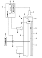
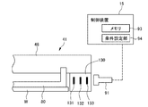
- the elastic film 80 is provided with sensors 85 and 86 having a communication function.
- One sensor 85 is provided in the vicinity of the portion in contact with the wafer W, and the other sensor 86 is attached to the side wall 80 a of the elastic film 80.
- the sensor 85 is provided so as to be embedded in the elastic film 80.
- the position of the sensor 85 is not particularly limited. You may arrange
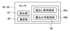
- the sensors 85 and 86 include a detection unit 87, a memory 88, and a communication unit 89.
- the detector 87 is, for example, a strain sensor, detects the amount of strain applied to the sensor, and outputs it as strain information.
- the sensor is not limited to a strain sensor, and for example, a temperature sensor, an acceleration sensor, or a tilt sensor can be used.
- the memory 88 is provided with a read-only area 88a in which predetermined data is stored in advance, and a writable / writable area 88b.
- the read-only area 88a contains a consumable elastic film 80.
- Information such as a part number (part ID), a serial number, an expiration date, shipment inspection data, and manufacturing data is stored.
- the shipment inspection data includes rubber physical property inspection data, outer dimension data, and swell measurement data of the elastic membrane
- the manufacturing data includes press pressure, press temperature, press time, secondary vulcanization temperature, Data on processing conditions such as secondary vulcanization time are included.
- the wafer processing data includes information on the use start date, the last use date, the total number of wafers processed, and the total processing time of the substrate processing apparatus after the elastic film 80 as a consumable is replaced.
- the communication unit 89 is, for example, a wireless communication module, and exchanges data stored in the read-only area 88a and the writable area 88b with the detectors 90 and 91 (see FIG. 4) provided in the substrate processing apparatus 10. Perform read processing.
- the detectors 90 and 91 are communication modules capable of wireless communication with the communication unit 89, and are a reading position located in the vicinity of the corresponding sensors 85 and 86, and a standby position for retreating from the moving area of the top ring 41. Between the sensors 85 and 86, and data is transmitted to and received from the sensors 85 and 86 at a timing when the substrate processing by the substrate processing apparatus 10 is not performed.
- the control device 15 is directly connected to the detectors 90 and 91 by wire or wirelessly, and has a memory 93 for storing various data read from the sensors 85 and 86, and a shipment read from the sensors 85 and 86.
- a condition setting unit 94 is provided for setting substrate processing conditions (recipes and machine constants) based on inspection data and manufacturing data.
- the memory 93 of the control device 15 stores a program for controlling the operation of each component of the substrate processing apparatus 10 including the detectors 90 and 91 and the condition setting unit 94. The operation of the substrate processing apparatus 10 is controlled by being read during the operation. In addition, you may make it connect the control apparatus 15 and the detectors 90 and 91 via the internet or another communication apparatus.
- the control device 15 detects the output from the sensors 85 and 86 when no load (pressure) is applied to the elastic membrane 80 or when a predetermined pressure is applied, and the sensor output at that time is zero. Can be set as
- FIG. 6 is a flowchart showing a verification processing procedure when the elastic film 80 to which the sensors 85 and 86 are attached is attached to the substrate processing apparatus 10.
- the controller 15 of the substrate processing apparatus 10 detects that the elastic film 80, which is a consumable, is attached to the apparatus main body by repair or replacement (step S10), it drives both or one of the detectors 90 and 91. Then, the component ID (part number) stored in the corresponding sensor 85, 86 is read (step S11).
- the control device 15 determines whether or not the read component ID matches the component ID stored in advance in the memory 93 in the substrate processing apparatus 10 (step S12). When the read component ID does not match any of the component IDs stored in the memory 93 (for example, when an elastic film that does not match the substrate processing apparatus 10 is set by mistake, When set, the control device 15 interlocks the substrate processing apparatus 10 so that the substrate polishing process cannot be performed by the polishing unit 40 using the elastic film (step S13).
- the control device 15 sends the shipping inspection data and manufacturing data of the elastic film 80 stored in the memory 88. Is stored in the memory 93 in the control device 15 (step S14). The control device 15 sets a substrate polishing recipe and a machine constant of the device based on various data read from the memory 88 (step S15). Thereafter, the control device 15 drives the polishing unit to start the polishing process for the wafer W (step S16).
- FIG. 7 is a flowchart showing the operation of the substrate polishing process.
- the sensors 85 and 86 detect the amount of strain generated in the elastic film 80 every predetermined time during polishing (step S21), and the memory 88 is stored as strain amount data. Is recorded in the writing area 88b (step S22).
- the control device 15 determines whether or not the polishing process of the substrate is finished (step S23), and when the polishing process is finished, the detectors 90 and 91 are driven and stored in the memory 88 of the elastic film 80.
- the stored distortion amount data is read out and stored in the memory 93 in the control device 15 (step S24).
- the control device 15 sets a polishing recipe to be applied when polishing the next wafer W based on the read distortion amount data (step S25). For example, the elongation amount of the elastic film 80 is calculated from the read strain amount data, and is corrected using the rubber physical property inspection data, the external dimension data, and the bulge measurement data read when the elastic film 80 is set. Thus, the polishing recipe can be set. Thereafter, the control device 15 drives the polishing unit to start the polishing process for the wafer W (step S26).
- the polishing recipe used at the time of polishing the next wafer W is set from the distortion amount data.
- the distortion amount is determined from the set value.
- the pressure in the pressure chamber 81 may be adjusted by adjusting the opening amount of the valve 82 so that the distortion amount approaches the set value.
- the distortion amount data recorded in the memory 88 of the sensors 85 and 86 may be erased when being read out by the control device 15, whereby the data capacity in the memory 88 can be suppressed.
- FIG. 8 shows a processing procedure in the case where troubles such as poor polishing performance (for example, abnormal polishing rate, abnormal polishing profile, abnormal step performance of the pattern on the wafer), wafer slipout, and wafer cracking occur in the substrate processing apparatus 10. It is a flowchart which shows.
- poor polishing performance for example, abnormal polishing rate, abnormal polishing profile, abnormal step performance of the pattern on the wafer
- wafer slipout and wafer cracking occur in the substrate processing apparatus 10.
- the controller 15 When the controller 15 detects that some trouble has occurred in the polishing unit (step S30), it immediately ends the polishing process currently being executed and stops the operation of the substrate processing apparatus (step S31).
- the control device 15 drives the detectors 90 and 91 to read various information (for example, the number of wafers processed, the processing time, the start / end date of use, the machine count) from the memory in the control device 15. Constants and recipe information) are read from the memory 93 in the apparatus (step S32), and are written in the memory 88 in the sensors 85 and 86 attached to the elastic film 80 (step S33).
- the lock of the top ring 41 is released, and the elastic film 80 is removed from the top ring 41.
- the removed elastic film 80 is set in an offline reader (not shown) and recorded in the memory 88 in the sensors 88 and 86 attached to the elastic film 80 in the various information written in step S33 and in the memory 88.
- distortion amount data during the substrate polishing process is read (step S34).
- the cause of the failure can be diagnosed by analyzing the various information and distortion amount data that have been read (step S35). Note that, when diagnosing the cause of the failure, the rubber properties, outer dimensions, and swelling of the extracted elastic film 80 may be inspected.
- the present invention is not limited to this, for example, as shown in FIG. As described above, the present invention can also be applied when the wafer W after the polishing process is detached from the elastic film.
- a gas injection unit 100 connected to the control device 15 is disposed in the vicinity of the top ring 41. Since the wafer W immediately after the polishing process is adsorbed by the elastic film 80, the wafer W cannot be detached from the elastic film 80 as it is. Therefore, the gas injection unit 100 is, for example, non-volatile toward the vicinity of the bonding portion between the wafer W and the elastic film 80 (the swollen portion near the side wall portion of the elastic film) at a predetermined timing after the polishing process is completed. Inject gas. As a result, the wafer W that has undergone the polishing process can be detached from the elastic film 80. Note that liquid (pure water) may be ejected instead of gas.
- the position of the bulging portion of the elastic film 80 (the vertical position in the figure) is not always constant, and the elastic film manufacturing conditions, rubber physical property inspection data, appearance dimension data, number of processed substrates, processing time, pressure chamber It fluctuates according to the pressure of 81 or the like.
- the gas from the gas injection unit 100 is injected to a position shifted from the boundary between the elastic film 80 and the substrate, the wafer W after the polishing process cannot be easily detached from the elastic film 80. .
- the valve 82 is driven to stop the fluid supply from the fluid supply source 83. Therefore, when the wafer W is detached from the elastic film after the polishing process is finished, the pressure in the pressure chamber 81 becomes constant and the position of the bulging portion of the elastic film 80 becomes constant. It can be reliably applied to the boundary between the elastic film 80 and the wafer W.
- FIG. 10 shows another example of a configuration in which the polished wafer W is detached from the elastic film.
- a gas injection unit 140 and an imaging unit 141 connected to the control device 15 are arranged in the vicinity of the top ring 41.
- the gas injection unit 140 can adjust the injection angle, and the imaging unit 141 images a boundary portion between the wafer W and the elastic film.
- An image obtained by imaging is sent to the image processing unit 142 in the control device 15.
- the image processing unit 142 detects the position of the boundary portion between the wafer W and the elastic film (the position in the direction in which the wafer W is detached from the elastic film) based on the image captured by the imaging unit 141.
- the injection angle adjustment unit 143 is configured to detect the gas injection angle of the gas injection unit 140 based on the position information of the boundary between the wafer W and the elastic film obtained in the image processing unit 142 and the installation position information of the gas injection unit 140. And the injection angle of the gas injection unit 140 is adjusted. Thereby, the gas from the gas injection unit 140 can be reliably applied to the boundary between the elastic film 80 and the wafer W.
- the present invention is not limited to this, and a plurality of sensors are disposed and elastic. You may make it detect the distortion amount in several places of a film
- an elastic film 102 for forming a plurality of pressure chambers 101a to 101d is provided between the top ring 41, and a plurality of sensors 103a to 103d are provided at positions corresponding to the pressure chambers. It may be.
- the internal pressures of the pressure chambers 101a to 101d are made uniform by controlling the valves 104a to 104d connected to the fluid supply source 83 so that the distortion amounts detected by the sensors 103a to 103d are constant. Can be adjusted.
- the shape of the elastic membrane applied to the present invention is not particularly limited.
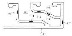
- the sensors 113 to 117 may be arranged.
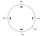
- a plurality of sensors 121 to 124 may be arranged along the circumferential direction of the elastic film 120. Thereby, the distribution of elongation of the elastic film can be detected accurately.
- the present invention is not limited to this, and the sensor may be disposed on the retainer ring as shown in FIG. In FIG. 14, three sensors 131 to 133 are embedded in the retainer ring 130, and these sensors 131 to 133 detect the amount of strain received during the polishing process, similar to those used in the above-described embodiment. In addition, various information is transmitted to and received from the control device 15 via the detector 91.
- the plurality of sensors 131 to 133 are embedded in the retainer ring 130 according to the present embodiment, distortions detected by the plurality of sensors 131 to 133 when performing polishing using a dummy wafer. The amount can be monitored. Then, as shown in FIG. 15 (b), when the displacement of the distortion amounts (arrows in the figure) from these sensors 131 to 133 falls within a predetermined value, the test polishing with the dummy wafer is terminated, whereby the retainer Break-in processing can be performed reliably regardless of the difference in ring material and polishing conditions.
- the break-in process is controlled using a plurality of strain sensors provided in the retainer ring 130, but the present invention is not limited to this, and for example, a plurality of strain sensors.
- the substrate processing conditions such as the pressure in the elastic film may be changed as appropriate according to the variation in strain information.
- control device acquires information on the type of consumables such as elastic membranes or retainer rings, the replacement time, and the number of strain measurements, and on the basis of these information, the maintenance date and time (or the time until maintenance) of the substrate processing apparatus is acquired. Time) may be calculated and displayed. As a result, the operator can appropriately grasp the maintenance timing of the apparatus.
- control device may be configured to automatically order consumables such as an elastic membrane and a retainer ring when the calculated maintenance date and time approaches (for example, several days ago). Sometimes a consumable can be reliably prepared.
- a program that causes the control device to calculate the maintenance date and place an order for consumables may be stored in advance in the memory of the control device, or may be installed later via the Internet or the like. good.
- a communication function may be provided in the control device so that it can be connected to an external server via a network, and various information such as the operating status of the device, strain data, and polishing environment information may be transmitted to the external server.
- the external server may be configured so that the control pattern of the substrate processing apparatus is standardized and automatically operated while adjusting polishing conditions such as polishing pressure based on various data received from the control apparatus. Further, it may be configured to be connectable to other substrate processing via a network, and may share various information such as the operating status of the apparatus, strain data, and polishing environment information.
- abnormality detection of the substrate processing apparatus and consumables used in the substrate processing apparatus is performed based on various types of information sent from the substrate processing apparatus and various types of information from other substrate processing apparatuses. Further, life prediction and determination may be performed, and abnormality detection and life display may be performed. Furthermore, it is possible to perform control for stabilizing the performance of the substrate processing apparatus in the external server.
- distortion data and other output data sent from the sensor are automatically learned by extracting feature values and the control pattern is automatically standardized to predict, judge, and display abnormalities and lifetimes. You may make it do.
- the format may be standardized in communication, device interface, etc., and the device / device management may be performed using information communication between the device / device.
- the elongation distribution of the consumables is measured using a strain sensor.
- the type of sensor is not limited, and for example, the temperature distribution may be measured using a temperature sensor, or The pressure distribution may be measured using a pressure sensor. Further, a plurality of types of sensors may be used in combination.
- the substrate polishing apparatus for polishing the wafer W has been described as an example.
- the present invention is not limited to this, and for example, as a consumable in a substrate cleaning apparatus that cleans a substrate after polishing processing.
Priority Applications (4)
| Application Number | Priority Date | Filing Date | Title |
|---|---|---|---|
| KR1020197030937A KR102474471B1 (ko) | 2017-03-31 | 2018-01-16 | 기판 처리 장치 |
| US16/499,576 US11969858B2 (en) | 2017-03-31 | 2018-01-16 | Substrate processing apparatus |
| SG11201908780R SG11201908780RA (en) | 2017-03-31 | 2018-01-16 | Substrate processing apparatus |
| CN201880022273.2A CN110476226B (zh) | 2017-03-31 | 2018-01-16 | 基板处理装置 |
Applications Claiming Priority (2)
| Application Number | Priority Date | Filing Date | Title |
|---|---|---|---|
| JP2017-071573 | 2017-03-31 | ||
| JP2017071573A JP6990980B2 (ja) | 2017-03-31 | 2017-03-31 | 基板処理装置 |
Publications (1)
| Publication Number | Publication Date |
|---|---|
| WO2018179685A1 true WO2018179685A1 (ja) | 2018-10-04 |
Family
ID=63677702
Family Applications (1)
| Application Number | Title | Priority Date | Filing Date |
|---|---|---|---|
| PCT/JP2018/000912 WO2018179685A1 (ja) | 2017-03-31 | 2018-01-16 | 基板処理装置 |
Country Status (7)
| Country | Link |
|---|---|
| US (1) | US11969858B2 (zh) |
| JP (1) | JP6990980B2 (zh) |
| KR (1) | KR102474471B1 (zh) |
| CN (1) | CN110476226B (zh) |
| SG (1) | SG11201908780RA (zh) |
| TW (1) | TWI758436B (zh) |
| WO (1) | WO2018179685A1 (zh) |
Families Citing this family (7)
| Publication number | Priority date | Publication date | Assignee | Title |
|---|---|---|---|---|
| KR102629679B1 (ko) * | 2018-11-09 | 2024-01-29 | 주식회사 케이씨텍 | 연마 장치용 캐리어 헤드 및 이에 사용되는 멤브레인 |
| JP2022080370A (ja) * | 2020-11-18 | 2022-05-30 | 株式会社荏原製作所 | 基板保持装置 |
| WO2022187055A1 (en) * | 2021-03-05 | 2022-09-09 | Applied Materials, Inc. | Machine learning for classifying retaining rings |
| TWI789926B (zh) * | 2021-09-28 | 2023-01-11 | 中國砂輪企業股份有限公司 | 研磨系統、研磨狀態感測系統及其資料庫與方法 |
| WO2023162714A1 (ja) * | 2022-02-25 | 2023-08-31 | 株式会社荏原製作所 | 基板研磨装置 |
| JP2023148615A (ja) * | 2022-03-30 | 2023-10-13 | 株式会社荏原製作所 | 情報処理装置、推論装置、機械学習装置、情報処理方法、推論方法、及び、機械学習方法 |
| JP2023162749A (ja) * | 2022-04-27 | 2023-11-09 | 株式会社荏原製作所 | 弾性膜の初期化装置、研磨装置、弾性膜の初期化方法、および弾性膜の寿命判定方法 |
Citations (8)
| Publication number | Priority date | Publication date | Assignee | Title |
|---|---|---|---|---|
| WO2000045993A1 (fr) * | 1999-02-02 | 2000-08-10 | Ebara Corporation | Dispositif de maintien et de polissage de plaquette |
| JP2001009712A (ja) * | 1999-06-22 | 2001-01-16 | Mitsubishi Materials Corp | ウェーハ研磨装置及びウェーハ製造方法 |
| JP2008310404A (ja) * | 2007-06-12 | 2008-12-25 | Nikon Corp | 研磨装置 |
| JP2009542449A (ja) * | 2006-06-28 | 2009-12-03 | スリーエム イノベイティブ プロパティズ カンパニー | 研磨物品、cmpモニタリングシステム及び方法 |
| JP2011194509A (ja) * | 2010-03-19 | 2011-10-06 | Nitta Haas Inc | 研磨装置、研磨パッドおよび研磨情報管理システム |
| JP2014011432A (ja) * | 2012-07-03 | 2014-01-20 | Ebara Corp | 研磨装置および研磨方法 |
| JP2014223684A (ja) * | 2013-05-15 | 2014-12-04 | 株式会社東芝 | 研磨装置および研磨方法 |
| JP2015051501A (ja) * | 2010-09-30 | 2015-03-19 | 株式会社荏原製作所 | 研磨装置および方法 |
Family Cites Families (17)
| Publication number | Priority date | Publication date | Assignee | Title |
|---|---|---|---|---|
| TW436382B (en) | 1999-03-12 | 2001-05-28 | Mitsubishi Materials Corp | Wafer holding head, wafer polishing apparatus, and method for making wafers |
| US6494765B2 (en) | 2000-09-25 | 2002-12-17 | Center For Tribology, Inc. | Method and apparatus for controlled polishing |
| JP2002219645A (ja) | 2000-11-21 | 2002-08-06 | Nikon Corp | 研磨装置、この研磨装置を用いた半導体デバイス製造方法並びにこの製造方法によって製造された半導体デバイス |
| JP2005123485A (ja) | 2003-10-17 | 2005-05-12 | Ebara Corp | 研磨装置 |
| JP4994227B2 (ja) * | 2004-06-21 | 2012-08-08 | 株式会社荏原製作所 | 研磨装置および研磨方法 |
| TW200610615A (en) | 2004-07-15 | 2006-04-01 | Disco Corp | Grindstone tool |
| US20090053983A1 (en) | 2006-01-25 | 2009-02-26 | Jsr Corporation | Chemical mechanical polishing pad and method for manufacturing same |
| DE102007011880A1 (de) | 2007-03-13 | 2008-09-18 | Peter Wolters Gmbh | Bearbeitungsmaschine mit Mitteln zur Erfassung von Bearbeitungsparametern |
| JP5552401B2 (ja) * | 2010-09-08 | 2014-07-16 | 株式会社荏原製作所 | 研磨装置および方法 |
| JP5868081B2 (ja) * | 2011-09-05 | 2016-02-24 | 株式会社ディスコ | 加工装置 |
| US9105516B2 (en) | 2012-07-03 | 2015-08-11 | Ebara Corporation | Polishing apparatus and polishing method |
| US20140020829A1 (en) | 2012-07-18 | 2014-01-23 | Applied Materials, Inc. | Sensors in Carrier Head of a CMP System |
| WO2014078151A1 (en) | 2012-11-16 | 2014-05-22 | Applied Materials, Inc. | Recording measurements by sensors for a carrier head |
| US9454684B2 (en) | 2014-05-28 | 2016-09-27 | Taiwan Semiconductor Manufacturing Company Limited | Edge crack detection system |
| US9878421B2 (en) | 2014-06-16 | 2018-01-30 | Applied Materials, Inc. | Chemical mechanical polishing retaining ring with integrated sensor |
| KR101913701B1 (ko) * | 2015-03-13 | 2018-11-02 | 주식회사 케이씨텍 | 화학 기계적 연마 장치의 캐리어 헤드 |
| JP6557049B2 (ja) * | 2015-04-23 | 2019-08-07 | 株式会社ディスコ | 加工装置 |
-
2017
- 2017-03-31 JP JP2017071573A patent/JP6990980B2/ja active Active
-
2018
- 2018-01-16 KR KR1020197030937A patent/KR102474471B1/ko active IP Right Grant
- 2018-01-16 CN CN201880022273.2A patent/CN110476226B/zh active Active
- 2018-01-16 US US16/499,576 patent/US11969858B2/en active Active
- 2018-01-16 SG SG11201908780R patent/SG11201908780RA/en unknown
- 2018-01-16 WO PCT/JP2018/000912 patent/WO2018179685A1/ja active Application Filing
- 2018-03-15 TW TW107108771A patent/TWI758436B/zh active
Patent Citations (8)
| Publication number | Priority date | Publication date | Assignee | Title |
|---|---|---|---|---|
| WO2000045993A1 (fr) * | 1999-02-02 | 2000-08-10 | Ebara Corporation | Dispositif de maintien et de polissage de plaquette |
| JP2001009712A (ja) * | 1999-06-22 | 2001-01-16 | Mitsubishi Materials Corp | ウェーハ研磨装置及びウェーハ製造方法 |
| JP2009542449A (ja) * | 2006-06-28 | 2009-12-03 | スリーエム イノベイティブ プロパティズ カンパニー | 研磨物品、cmpモニタリングシステム及び方法 |
| JP2008310404A (ja) * | 2007-06-12 | 2008-12-25 | Nikon Corp | 研磨装置 |
| JP2011194509A (ja) * | 2010-03-19 | 2011-10-06 | Nitta Haas Inc | 研磨装置、研磨パッドおよび研磨情報管理システム |
| JP2015051501A (ja) * | 2010-09-30 | 2015-03-19 | 株式会社荏原製作所 | 研磨装置および方法 |
| JP2014011432A (ja) * | 2012-07-03 | 2014-01-20 | Ebara Corp | 研磨装置および研磨方法 |
| JP2014223684A (ja) * | 2013-05-15 | 2014-12-04 | 株式会社東芝 | 研磨装置および研磨方法 |
Also Published As
| Publication number | Publication date |
|---|---|
| JP6990980B2 (ja) | 2022-01-12 |
| TW201836763A (zh) | 2018-10-16 |
| KR20190134665A (ko) | 2019-12-04 |
| TWI758436B (zh) | 2022-03-21 |
| US11969858B2 (en) | 2024-04-30 |
| JP2018174230A (ja) | 2018-11-08 |
| US20200023487A1 (en) | 2020-01-23 |
| KR102474471B1 (ko) | 2022-12-06 |
| CN110476226B (zh) | 2023-08-18 |
| CN110476226A (zh) | 2019-11-19 |
| SG11201908780RA (en) | 2019-10-30 |
Similar Documents
| Publication | Publication Date | Title |
|---|---|---|
| WO2018179685A1 (ja) | 基板処理装置 | |
| US9403256B2 (en) | Recording measurements by sensors for a carrier head | |
| CN108723976B (zh) | 泄漏检测方法、以及非暂时性的计算机可读取记录介质 | |
| TWI449595B (zh) | 研磨方法及研磨裝置 | |
| US20100029178A1 (en) | Smart conditioner rinse station | |
| KR101972647B1 (ko) | 연마 장치 및 연마 방법 | |
| US20140134924A1 (en) | Substrate holding apparatus and polishing apparatus | |
| TW202232600A (zh) | 經由定向的晶圓裝載作不對稱性校正 | |
| CN109807739A (zh) | 化学机械研磨设备 | |
| US11407081B2 (en) | Substrate processing apparatus | |
| JP6906425B2 (ja) | 基板処理装置 | |
| KR102415299B1 (ko) | 기판 처리 시스템 | |
| WO2023210073A1 (ja) | 弾性膜の初期化装置、研磨装置、弾性膜の初期化方法、および弾性膜の寿命判定方法 | |
| TW201324600A (zh) | 化學機械研磨製程及化學機械研磨系統 | |
| JP2017187311A (ja) | リーク検査装置 |
Legal Events
| Date | Code | Title | Description |
|---|---|---|---|
| 121 | Ep: the epo has been informed by wipo that ep was designated in this application |
Ref document number: 18774387 Country of ref document: EP Kind code of ref document: A1 |
|
| NENP | Non-entry into the national phase |
Ref country code: DE |
|
| ENP | Entry into the national phase |
Ref document number: 20197030937 Country of ref document: KR Kind code of ref document: A |
|
| 122 | Ep: pct application non-entry in european phase |
Ref document number: 18774387 Country of ref document: EP Kind code of ref document: A1 |