WO2018179685A1 - Substrate processing device - Google Patents
Substrate processing device Download PDFInfo
- Publication number
- WO2018179685A1 WO2018179685A1 PCT/JP2018/000912 JP2018000912W WO2018179685A1 WO 2018179685 A1 WO2018179685 A1 WO 2018179685A1 JP 2018000912 W JP2018000912 W JP 2018000912W WO 2018179685 A1 WO2018179685 A1 WO 2018179685A1
- Authority
- WO
- WIPO (PCT)
- Prior art keywords
- substrate
- polishing
- elastic film
- sensor
- processing apparatus
- Prior art date
Links
Images


Classifications
-
- B—PERFORMING OPERATIONS; TRANSPORTING
- B24—GRINDING; POLISHING
- B24B—MACHINES, DEVICES, OR PROCESSES FOR GRINDING OR POLISHING; DRESSING OR CONDITIONING OF ABRADING SURFACES; FEEDING OF GRINDING, POLISHING, OR LAPPING AGENTS
- B24B37/00—Lapping machines or devices; Accessories
- B24B37/27—Work carriers
- B24B37/30—Work carriers for single side lapping of plane surfaces
-
- B—PERFORMING OPERATIONS; TRANSPORTING
- B24—GRINDING; POLISHING
- B24B—MACHINES, DEVICES, OR PROCESSES FOR GRINDING OR POLISHING; DRESSING OR CONDITIONING OF ABRADING SURFACES; FEEDING OF GRINDING, POLISHING, OR LAPPING AGENTS
- B24B49/00—Measuring or gauging equipment for controlling the feed movement of the grinding tool or work; Arrangements of indicating or measuring equipment, e.g. for indicating the start of the grinding operation
- B24B49/10—Measuring or gauging equipment for controlling the feed movement of the grinding tool or work; Arrangements of indicating or measuring equipment, e.g. for indicating the start of the grinding operation involving electrical means
-
- H—ELECTRICITY
- H01—ELECTRIC ELEMENTS
- H01L—SEMICONDUCTOR DEVICES NOT COVERED BY CLASS H10
- H01L21/00—Processes or apparatus adapted for the manufacture or treatment of semiconductor or solid state devices or of parts thereof
- H01L21/02—Manufacture or treatment of semiconductor devices or of parts thereof
- H01L21/04—Manufacture or treatment of semiconductor devices or of parts thereof the devices having at least one potential-jump barrier or surface barrier, e.g. PN junction, depletion layer or carrier concentration layer
- H01L21/18—Manufacture or treatment of semiconductor devices or of parts thereof the devices having at least one potential-jump barrier or surface barrier, e.g. PN junction, depletion layer or carrier concentration layer the devices having semiconductor bodies comprising elements of Group IV of the Periodic System or AIIIBV compounds with or without impurities, e.g. doping materials
- H01L21/30—Treatment of semiconductor bodies using processes or apparatus not provided for in groups H01L21/20 - H01L21/26
- H01L21/302—Treatment of semiconductor bodies using processes or apparatus not provided for in groups H01L21/20 - H01L21/26 to change their surface-physical characteristics or shape, e.g. etching, polishing, cutting
- H01L21/304—Mechanical treatment, e.g. grinding, polishing, cutting
-
- H—ELECTRICITY
- H01—ELECTRIC ELEMENTS
- H01L—SEMICONDUCTOR DEVICES NOT COVERED BY CLASS H10
- H01L21/00—Processes or apparatus adapted for the manufacture or treatment of semiconductor or solid state devices or of parts thereof
- H01L21/02—Manufacture or treatment of semiconductor devices or of parts thereof
- H01L21/04—Manufacture or treatment of semiconductor devices or of parts thereof the devices having at least one potential-jump barrier or surface barrier, e.g. PN junction, depletion layer or carrier concentration layer
- H01L21/18—Manufacture or treatment of semiconductor devices or of parts thereof the devices having at least one potential-jump barrier or surface barrier, e.g. PN junction, depletion layer or carrier concentration layer the devices having semiconductor bodies comprising elements of Group IV of the Periodic System or AIIIBV compounds with or without impurities, e.g. doping materials
- H01L21/30—Treatment of semiconductor bodies using processes or apparatus not provided for in groups H01L21/20 - H01L21/26
- H01L21/302—Treatment of semiconductor bodies using processes or apparatus not provided for in groups H01L21/20 - H01L21/26 to change their surface-physical characteristics or shape, e.g. etching, polishing, cutting
- H01L21/306—Chemical or electrical treatment, e.g. electrolytic etching
- H01L21/30625—With simultaneous mechanical treatment, e.g. mechanico-chemical polishing
-
- H—ELECTRICITY
- H01—ELECTRIC ELEMENTS
- H01L—SEMICONDUCTOR DEVICES NOT COVERED BY CLASS H10
- H01L21/00—Processes or apparatus adapted for the manufacture or treatment of semiconductor or solid state devices or of parts thereof
- H01L21/67—Apparatus specially adapted for handling semiconductor or electric solid state devices during manufacture or treatment thereof; Apparatus specially adapted for handling wafers during manufacture or treatment of semiconductor or electric solid state devices or components ; Apparatus not specifically provided for elsewhere
- H01L21/67005—Apparatus not specifically provided for elsewhere
- H01L21/67011—Apparatus for manufacture or treatment
- H01L21/67092—Apparatus for mechanical treatment
-
- H—ELECTRICITY
- H01—ELECTRIC ELEMENTS
- H01L—SEMICONDUCTOR DEVICES NOT COVERED BY CLASS H10
- H01L21/00—Processes or apparatus adapted for the manufacture or treatment of semiconductor or solid state devices or of parts thereof
- H01L21/67—Apparatus specially adapted for handling semiconductor or electric solid state devices during manufacture or treatment thereof; Apparatus specially adapted for handling wafers during manufacture or treatment of semiconductor or electric solid state devices or components ; Apparatus not specifically provided for elsewhere
- H01L21/67005—Apparatus not specifically provided for elsewhere
- H01L21/67011—Apparatus for manufacture or treatment
- H01L21/67155—Apparatus for manufacturing or treating in a plurality of work-stations
- H01L21/67207—Apparatus for manufacturing or treating in a plurality of work-stations comprising a chamber adapted to a particular process
- H01L21/67219—Apparatus for manufacturing or treating in a plurality of work-stations comprising a chamber adapted to a particular process comprising at least one polishing chamber
-
- H—ELECTRICITY
- H01—ELECTRIC ELEMENTS
- H01L—SEMICONDUCTOR DEVICES NOT COVERED BY CLASS H10
- H01L21/00—Processes or apparatus adapted for the manufacture or treatment of semiconductor or solid state devices or of parts thereof
- H01L21/67—Apparatus specially adapted for handling semiconductor or electric solid state devices during manufacture or treatment thereof; Apparatus specially adapted for handling wafers during manufacture or treatment of semiconductor or electric solid state devices or components ; Apparatus not specifically provided for elsewhere
- H01L21/67005—Apparatus not specifically provided for elsewhere
- H01L21/67242—Apparatus for monitoring, sorting or marking
- H01L21/67259—Position monitoring, e.g. misposition detection or presence detection
-
- H—ELECTRICITY
- H01—ELECTRIC ELEMENTS
- H01L—SEMICONDUCTOR DEVICES NOT COVERED BY CLASS H10
- H01L21/00—Processes or apparatus adapted for the manufacture or treatment of semiconductor or solid state devices or of parts thereof
- H01L21/67—Apparatus specially adapted for handling semiconductor or electric solid state devices during manufacture or treatment thereof; Apparatus specially adapted for handling wafers during manufacture or treatment of semiconductor or electric solid state devices or components ; Apparatus not specifically provided for elsewhere
- H01L21/67005—Apparatus not specifically provided for elsewhere
- H01L21/67242—Apparatus for monitoring, sorting or marking
- H01L21/67294—Apparatus for monitoring, sorting or marking using identification means, e.g. labels on substrates or labels on containers
-
- H—ELECTRICITY
- H01—ELECTRIC ELEMENTS
- H01L—SEMICONDUCTOR DEVICES NOT COVERED BY CLASS H10
- H01L22/00—Testing or measuring during manufacture or treatment; Reliability measurements, i.e. testing of parts without further processing to modify the parts as such; Structural arrangements therefor
- H01L22/20—Sequence of activities consisting of a plurality of measurements, corrections, marking or sorting steps
- H01L22/26—Acting in response to an ongoing measurement without interruption of processing, e.g. endpoint detection, in-situ thickness measurement
-
- B—PERFORMING OPERATIONS; TRANSPORTING
- B23—MACHINE TOOLS; METAL-WORKING NOT OTHERWISE PROVIDED FOR
- B23Q—DETAILS, COMPONENTS, OR ACCESSORIES FOR MACHINE TOOLS, e.g. ARRANGEMENTS FOR COPYING OR CONTROLLING; MACHINE TOOLS IN GENERAL CHARACTERISED BY THE CONSTRUCTION OF PARTICULAR DETAILS OR COMPONENTS; COMBINATIONS OR ASSOCIATIONS OF METAL-WORKING MACHINES, NOT DIRECTED TO A PARTICULAR RESULT
- B23Q15/00—Automatic control or regulation of feed movement, cutting velocity or position of tool or work
- B23Q15/007—Automatic control or regulation of feed movement, cutting velocity or position of tool or work while the tool acts upon the workpiece
- B23Q15/16—Compensation for wear of the tool
Definitions
- the present invention relates to a substrate processing apparatus for processing the surface of a substrate such as a semiconductor wafer.
- substrate processing apparatuses such as a substrate polishing apparatus for polishing a substrate such as a semiconductor wafer and a substrate cleaning apparatus for cleaning a substrate surface
- consumables such as a polishing pad are used.
- a polishing apparatus is known in which an RF tag that records information on the type and characteristics of these consumables is attached to the consumables, and the information is read when the apparatus is used (see Patent Document 1).
- Japanese Patent Laid-Open No. 2004-228688 discloses a case where the memory information of the RF tag is erased when a consumable such as a polishing pad is removed from the apparatus to prevent information leakage, and when an abnormality is detected by the abnormality monitoring unit. Discloses a polishing apparatus in which abnormal information is written in an RF tag.
- the present invention has been made in view of the above, and provides a substrate processing apparatus capable of making substrate processing conditions constant by more accurately detecting the status of consumables used for substrate processing. With the goal.
- One aspect of the present invention is a substrate processing apparatus that processes a substrate, the consumable used in the substrate processing apparatus, and a physical quantity of the consumable that is attached to the consumable and measures the physical quantity.
- At least one sensor provided with a storage unit and a communication unit for storing; a detector provided in the vicinity of the consumables; and a sensor for reading and writing information between the sensors attached to the consumables; and the detector
- a control device that sets processing conditions in the substrate processing apparatus based on a physical quantity of the consumables connected and read from the sensor.
- identification information of the sensor is stored in the storage unit, and the consumable is attached to the control device based on the identification information read from the sensor. Further, it is preferable to determine whether or not the substrate processing apparatus can be driven. In addition, it is preferable that information regarding the processing conditions of the substrate is recorded in a storage unit in the sensor when an abnormality occurs in the substrate processing apparatus.
- a substrate processing apparatus is a substrate polishing apparatus comprising: a polishing pad for polishing the substrate; and a substrate holding unit for holding the substrate and pressing the substrate against the polishing pad.
- the consumable is an elastic film that is attached to the substrate holding unit and holds a surface opposite to the polishing surface of the substrate, and the sensor is a strain sensor that measures strain of the elastic film, and the control device Can set processing conditions in the substrate processing apparatus based on the strain information of the elastic film measured by the strain sensor.
- At least one pressure chamber is formed between the elastic film and the substrate holding unit, and the control device is based on strain information of the elastic film measured by the strain sensor.
- the pressure in the pressure chamber is preferably adjusted. Due to variations in production of elastic membranes and variations in physical properties of raw material lots, even if pressure is applied at the same internal pressure, the elastic membrane does not swell in the same way, and the pressure applied to the substrate may vary depending on the individual elastic membrane. This variation can be canceled by adjusting the pressure.
- the substrate polishing apparatus includes an injection unit for separating the polished substrate from the elastic film by injecting gas or liquid onto the side wall of the elastic film holding the substrate.
- the control device may adjust the pressure in the pressure chamber based on strain information of the elastic film so that gas or liquid from the injection unit is injected to a boundary between the elastic film and the substrate. preferable. Thereby, gas or liquid can be effectively injected to the boundary between the elastic film and the substrate.
- the jetting unit is capable of adjusting the jetting angle of the gas or liquid, and from the image obtained by the imaging unit that images the boundary portion between the elastic film and the substrate, An image processing unit for detecting a position of the boundary part; and an injection angle adjusting unit for determining an injection angle by the injection unit based on the position of the boundary part detected by the image processing unit and adjusting the injection angle; It is preferable to provide.
- a substrate processing apparatus is a substrate polishing apparatus comprising: a polishing pad for polishing the substrate; and a substrate holding unit for holding the substrate and pressing the substrate against the polishing pad.
- the consumable is a retainer ring that supports the outer periphery of the substrate
- the sensor is a plurality of strain sensors that measure the strain of the retainer ring
- the control device detects the amount of strain detected by the plurality of strain sensors. It is preferable to detect whether or not the variation of the difference is within a predetermined value.
- the shape of the grounding surface of the retainer ring does not follow the polishing surface of the polishing pad, resulting in variations in how the retainer ring contacts the polishing surface.
- the compressive force applied in the vertical direction of the retainer ring also varies depending on the position of the ring. For this reason, the amount of strain detected by a plurality of strain sensors provided in the retainer ring also varies, but when the break-in of the retainer ring is completed, the shape of the retainer ring grounding surface follows the polishing surface of the pad. The variation in the amount of distortion detected by the plurality of strain sensors is reduced. Thereby, it is possible to effectively detect that the break-in of the retainer ring has been completed.
- a substrate processing apparatus is a substrate polishing apparatus comprising: a polishing pad for polishing the substrate; and a substrate holding unit for holding the substrate and pressing the substrate against the polishing pad.
- the consumable is a retainer ring that supports the outer periphery of the substrate
- the sensor is a plurality of strain sensors that measure the strain of the retainer ring
- the control device detects the amount of strain detected by the plurality of strain sensors.
- the processing conditions of the substrate are changed in accordance with the distribution of.
- a sensor for measuring the physical quantity of a consumable used in the substrate processing apparatus is attached to the consumable, and the processing conditions in the substrate processing apparatus are determined based on the physical quantity of the consumable read out from the sensor. Since it is set, the status of the consumables used for the substrate processing can be detected more accurately, and the substrate processing conditions can be made constant.
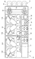
- FIG. 1 is a plan view showing the overall configuration of the substrate processing apparatus.
- the substrate processing apparatus 10 is divided into a load / unload unit 12, a polishing unit 13, and a cleaning unit 14, which are provided inside a rectangular housing 11.
- the substrate processing apparatus 10 also includes a control device 15 that controls operation of processing such as substrate transport, polishing, and cleaning.
- the load / unload unit 12 includes a plurality of front load units 20, a travel mechanism 21, and two transfer robots 22.
- a substrate cassette that stocks a large number of substrates (substrates) is placed on the front load unit 20.
- the transfer robot 22 has two hands up and down, and moves on the traveling mechanism 21 to take out the substrate W from the substrate cassette in the front load unit 20 and send it to the polishing unit 13, and from the cleaning unit 14. An operation of returning the processed substrate to be sent back to the substrate cassette is performed.
- the polishing unit 13 is an area for polishing (planarizing) the substrate, and is provided with a plurality of polishing units 13A to 13D, which are arranged along the longitudinal direction of the substrate processing apparatus.
- Each polishing unit includes a top ring for polishing the substrate W on the polishing table against the polishing pad, a polishing liquid supply nozzle for supplying a polishing liquid and a dressing liquid to the polishing pad, and a polishing surface of the polishing pad.
- a dresser that performs dressing and an atomizer that sprays a mixed fluid of liquid and gas or a mist-like liquid onto the polishing surface to wash away polishing debris and abrasive grains remaining on the polishing surface are provided.
- first and second linear transporters 16 and 17 are provided between the polishing unit 13 and the cleaning unit 14.
- the first linear transporter 16 has a first position for receiving the substrate W from the load / unload unit 12, second and third positions for transferring the substrate W between the polishing units 13A and 13B, and a second linear transporter. It is possible to move between a fourth position for delivering the substrate W to 17.
- the second linear transporter 17 is between the fifth position for receiving the substrate W from the first linear transporter 16 and the sixth and seventh positions for transferring the substrate W between the polishing units 13C and 13D. It is supposed to be movable.
- a swing transporter 23 for sending the substrate W to the cleaning unit 14 is provided between the transporters 16 and 17.
- the cleaning unit 14 includes a first substrate cleaning device 30, a second substrate cleaning device 31, a substrate drying device 32, and transfer robots 33 and 34 for transferring substrates between these devices.
- the substrate W that has been subjected to the polishing process by the polishing unit is cleaned (primary cleaning) by the first substrate cleaning device 30 and then further cleaned (finish cleaning) by the second substrate cleaning device 31.
- the cleaned substrate is transferred from the second substrate cleaning device 31 to the substrate drying device 32 and subjected to spin drying.
- the dried substrate W is returned to the load / unload unit 12.
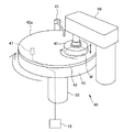
- FIG. 2 is a perspective view schematically showing the configuration of the polishing unit
- FIG. 3 is a side view schematically showing the configuration of the polishing unit.
- the polishing unit 40 holds a wafer (substrate) W and rotates it, a top ring (substrate holding device) 41, a polishing table 43 that instructs the polishing pad 42, and polishing that supplies slurry (polishing liquid) to the polishing pad 42.
- a liquid supply nozzle 45 and a film thickness sensor 47 that acquires a signal that changes according to the film thickness of the wafer W are provided.
- the top ring 41 is configured to hold the wafer W by vacuum suction on the lower surface thereof.
- the top ring 41 and the polishing table 43 rotate in the direction indicated by the arrow. In this state, the top ring 41 presses the wafer W against the upper polishing surface 42 a of the polishing pad 42. In the presence of the polishing liquid supplied from the polishing liquid supply nozzle 45 onto the polishing pad 42, the wafer W is slid in contact with the polishing pad 42 and polished.
- the film thickness sensor 47 is, for example, an optical sensor or an eddy current sensor, and is installed inside the polishing table 43. During polishing of the wafer W, the film thickness sensor 47 rotates with the polishing table 43 and acquires a film thickness signal corresponding to the film thickness when crossing the surface of the wafer W. The film thickness signal from the film thickness sensor 47 is transmitted to the control device 15, and the film thickness device 15 ends the polishing of the wafer W when the film thickness of the wafer W indicated by the film thickness signal reaches a set value.
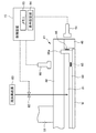
- the top ring 41 includes a head main body 48 that presses the wafer W against the polishing surface 42 a, and a retainer ring 49 that supports the outer periphery of the wafer W and prevents the wafer W from jumping out of the top ring 41. It has.
- the top ring 41 is connected to the top ring shaft 51, and a rotary joint 55 is attached to the upper end of the top ring shaft 51.
- the top ring shaft 51 is configured to move up and down with respect to the head arm 56 by a vertical movement mechanism 57, and is configured to move the entire top ring 51 up and down relative to the head arm 26.
- a vertical movement mechanism 67 that moves the top ring shaft 51 and the top ring 41 up and down includes a bridge 68 that rotatably supports the top ring shaft 51 via a bearing 66, a ball screw 72 attached to the bridge 68, and a column 70. And a servo motor 78 provided on the support base 69.
- a support base 69 that supports the servo motor 78 is fixed to the head arm 56 via a column 70.
- the ball screw 72 includes a screw shaft 72a connected to the servo motor 78, and a nut 72b into which the screw shaft 42a is screwed.
- the top ring shaft 51 moves up and down integrally with the bridge 68. Therefore, when the servo motor 78 is driven, the bridge 68 moves up and down via the ball screw 78, and thereby the top ring shaft 51 and the top ring 41 move up and down.
- the top ring shaft 51 is connected to the rotary cylinder 52 via a key (not shown).
- the rotary cylinder 52 includes a timing pulley 54 on the outer periphery thereof.
- a head motor 58 is fixed to the head arm 56, and the timing pulley 54 is connected to a timing pulley 60 provided in the head motor 58 via a timing belt 59.
- By rotating the head motor 58, the rotary cylinder 52 and the top ring shaft 51 rotate together via the timing pulley 60, the timing belt 59, and the timing pulley 54, and the top ring 11 rotates.
- the head arm 56 is supported by an arm shaft 61 that is rotatably supported by a frame (not shown).
- the operation of each component in the apparatus including the head motor 58 and the servo motor 78 constituting the polishing apparatus is controlled by the controller 15.
- the head arm 56 is configured to be pivotable about the arm shaft 61, and the top ring 41 holding the wafer W on the lower surface thereof is a polishing position above the polishing table 52 from the receiving position of the wafer W by the turning of the head arm 56. Moved to.
- the top ring 41 and the polishing table 42 are rotated, and the polishing liquid is supplied onto the polishing pad 42 from the polishing liquid supply nozzle 45.
- the top ring 41 is lowered to a predetermined position (height), and the wafer W is pressed against the polishing surface 42a of the polishing pad 42 at this predetermined position, so that the wafer W is brought into sliding contact with the polishing surface 42a.
- the surface is polished.
- the top ring main body 48 and the retainer ring 49 constituting the top ring 41 are configured to rotate integrally with the rotation of the top ring shaft 51.
- An elastic film (membrane) 80 that is in contact with the back surface of the wafer W is attached to the lower side of the top ring, and the lower surface of the elastic film 80 forms a substrate holding surface.
- the elastic membrane 80 has an annular partition wall 80 a extending in the vertical direction, whereby a pressure chamber 81 is formed between the elastic membrane 80 and the top ring body 48.
- the pressure chamber 81 is connected to a fluid supply source 83 via a valve 82, and pressurized fluid (gas) is supplied from the fluid supply source 83. Further, the control device 15 is connected to the valve 82, whereby the pressure in the pressure chamber 81 can be adjusted, and a negative pressure can be formed in the pressure chamber 82. Further, the pressure chamber 81 is connected to an atmosphere release mechanism (not shown), and the pressure chamber 81 can be opened to the atmosphere.
- the elastic film 80 has a through hole (not shown) at a position corresponding to the inner pressure chamber 81. By forming a negative pressure in the through hole, the wafer is formed on the substrate holding surface of the elastic film 80. W can be held.
- the elastic film 80 is formed of a rubber material having excellent strength and durability, such as ethylene propylene rubber (EPDM), polyurethane rubber, and silicone rubber.
- the retainer ring 49 is disposed so as to surround the top ring main body 48 and the elastic film 55.
- the retainer ring 49 is a ring-shaped member that comes into contact with the polishing surface 42a of the polishing pad 42, and is disposed so as to surround the outer peripheral edge of the wafer W held by the top ring main body 48. Supports the outer peripheral edge of the wafer W so as not to jump out of the top ring 41.
- the upper surface of the retainer ring 49 is connected to an annular retainer ring pressing mechanism (not shown), and a uniform downward load is applied to the entire upper surface of the retainer ring 49. As a result, the lower surface of the retainer ring 49 is pressed against the polishing surface 42 a of the polishing pad 42.
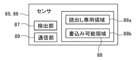
- the elastic film 80 is provided with sensors 85 and 86 having a communication function.
- One sensor 85 is provided in the vicinity of the portion in contact with the wafer W, and the other sensor 86 is attached to the side wall 80 a of the elastic film 80.
- the sensor 85 is provided so as to be embedded in the elastic film 80.
- the position of the sensor 85 is not particularly limited. You may arrange
- the sensors 85 and 86 include a detection unit 87, a memory 88, and a communication unit 89.
- the detector 87 is, for example, a strain sensor, detects the amount of strain applied to the sensor, and outputs it as strain information.
- the sensor is not limited to a strain sensor, and for example, a temperature sensor, an acceleration sensor, or a tilt sensor can be used.
- the memory 88 is provided with a read-only area 88a in which predetermined data is stored in advance, and a writable / writable area 88b.
- the read-only area 88a contains a consumable elastic film 80.
- Information such as a part number (part ID), a serial number, an expiration date, shipment inspection data, and manufacturing data is stored.
- the shipment inspection data includes rubber physical property inspection data, outer dimension data, and swell measurement data of the elastic membrane
- the manufacturing data includes press pressure, press temperature, press time, secondary vulcanization temperature, Data on processing conditions such as secondary vulcanization time are included.
- the wafer processing data includes information on the use start date, the last use date, the total number of wafers processed, and the total processing time of the substrate processing apparatus after the elastic film 80 as a consumable is replaced.
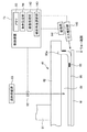
- the communication unit 89 is, for example, a wireless communication module, and exchanges data stored in the read-only area 88a and the writable area 88b with the detectors 90 and 91 (see FIG. 4) provided in the substrate processing apparatus 10. Perform read processing.
- the detectors 90 and 91 are communication modules capable of wireless communication with the communication unit 89, and are a reading position located in the vicinity of the corresponding sensors 85 and 86, and a standby position for retreating from the moving area of the top ring 41. Between the sensors 85 and 86, and data is transmitted to and received from the sensors 85 and 86 at a timing when the substrate processing by the substrate processing apparatus 10 is not performed.
- the control device 15 is directly connected to the detectors 90 and 91 by wire or wirelessly, and has a memory 93 for storing various data read from the sensors 85 and 86, and a shipment read from the sensors 85 and 86.
- a condition setting unit 94 is provided for setting substrate processing conditions (recipes and machine constants) based on inspection data and manufacturing data.
- the memory 93 of the control device 15 stores a program for controlling the operation of each component of the substrate processing apparatus 10 including the detectors 90 and 91 and the condition setting unit 94. The operation of the substrate processing apparatus 10 is controlled by being read during the operation. In addition, you may make it connect the control apparatus 15 and the detectors 90 and 91 via the internet or another communication apparatus.
- the control device 15 detects the output from the sensors 85 and 86 when no load (pressure) is applied to the elastic membrane 80 or when a predetermined pressure is applied, and the sensor output at that time is zero. Can be set as
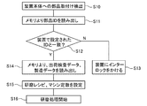
- FIG. 6 is a flowchart showing a verification processing procedure when the elastic film 80 to which the sensors 85 and 86 are attached is attached to the substrate processing apparatus 10.
- the controller 15 of the substrate processing apparatus 10 detects that the elastic film 80, which is a consumable, is attached to the apparatus main body by repair or replacement (step S10), it drives both or one of the detectors 90 and 91. Then, the component ID (part number) stored in the corresponding sensor 85, 86 is read (step S11).
- the control device 15 determines whether or not the read component ID matches the component ID stored in advance in the memory 93 in the substrate processing apparatus 10 (step S12). When the read component ID does not match any of the component IDs stored in the memory 93 (for example, when an elastic film that does not match the substrate processing apparatus 10 is set by mistake, When set, the control device 15 interlocks the substrate processing apparatus 10 so that the substrate polishing process cannot be performed by the polishing unit 40 using the elastic film (step S13).
- the control device 15 sends the shipping inspection data and manufacturing data of the elastic film 80 stored in the memory 88. Is stored in the memory 93 in the control device 15 (step S14). The control device 15 sets a substrate polishing recipe and a machine constant of the device based on various data read from the memory 88 (step S15). Thereafter, the control device 15 drives the polishing unit to start the polishing process for the wafer W (step S16).
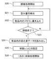
- FIG. 7 is a flowchart showing the operation of the substrate polishing process.
- the sensors 85 and 86 detect the amount of strain generated in the elastic film 80 every predetermined time during polishing (step S21), and the memory 88 is stored as strain amount data. Is recorded in the writing area 88b (step S22).
- the control device 15 determines whether or not the polishing process of the substrate is finished (step S23), and when the polishing process is finished, the detectors 90 and 91 are driven and stored in the memory 88 of the elastic film 80.
- the stored distortion amount data is read out and stored in the memory 93 in the control device 15 (step S24).
- the control device 15 sets a polishing recipe to be applied when polishing the next wafer W based on the read distortion amount data (step S25). For example, the elongation amount of the elastic film 80 is calculated from the read strain amount data, and is corrected using the rubber physical property inspection data, the external dimension data, and the bulge measurement data read when the elastic film 80 is set. Thus, the polishing recipe can be set. Thereafter, the control device 15 drives the polishing unit to start the polishing process for the wafer W (step S26).
- the polishing recipe used at the time of polishing the next wafer W is set from the distortion amount data.
- the distortion amount is determined from the set value.
- the pressure in the pressure chamber 81 may be adjusted by adjusting the opening amount of the valve 82 so that the distortion amount approaches the set value.
- the distortion amount data recorded in the memory 88 of the sensors 85 and 86 may be erased when being read out by the control device 15, whereby the data capacity in the memory 88 can be suppressed.
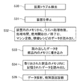
- FIG. 8 shows a processing procedure in the case where troubles such as poor polishing performance (for example, abnormal polishing rate, abnormal polishing profile, abnormal step performance of the pattern on the wafer), wafer slipout, and wafer cracking occur in the substrate processing apparatus 10. It is a flowchart which shows.
- poor polishing performance for example, abnormal polishing rate, abnormal polishing profile, abnormal step performance of the pattern on the wafer
- wafer slipout and wafer cracking occur in the substrate processing apparatus 10.
- the controller 15 When the controller 15 detects that some trouble has occurred in the polishing unit (step S30), it immediately ends the polishing process currently being executed and stops the operation of the substrate processing apparatus (step S31).
- the control device 15 drives the detectors 90 and 91 to read various information (for example, the number of wafers processed, the processing time, the start / end date of use, the machine count) from the memory in the control device 15. Constants and recipe information) are read from the memory 93 in the apparatus (step S32), and are written in the memory 88 in the sensors 85 and 86 attached to the elastic film 80 (step S33).
- the lock of the top ring 41 is released, and the elastic film 80 is removed from the top ring 41.
- the removed elastic film 80 is set in an offline reader (not shown) and recorded in the memory 88 in the sensors 88 and 86 attached to the elastic film 80 in the various information written in step S33 and in the memory 88.
- distortion amount data during the substrate polishing process is read (step S34).
- the cause of the failure can be diagnosed by analyzing the various information and distortion amount data that have been read (step S35). Note that, when diagnosing the cause of the failure, the rubber properties, outer dimensions, and swelling of the extracted elastic film 80 may be inspected.
- the present invention is not limited to this, for example, as shown in FIG. As described above, the present invention can also be applied when the wafer W after the polishing process is detached from the elastic film.
- a gas injection unit 100 connected to the control device 15 is disposed in the vicinity of the top ring 41. Since the wafer W immediately after the polishing process is adsorbed by the elastic film 80, the wafer W cannot be detached from the elastic film 80 as it is. Therefore, the gas injection unit 100 is, for example, non-volatile toward the vicinity of the bonding portion between the wafer W and the elastic film 80 (the swollen portion near the side wall portion of the elastic film) at a predetermined timing after the polishing process is completed. Inject gas. As a result, the wafer W that has undergone the polishing process can be detached from the elastic film 80. Note that liquid (pure water) may be ejected instead of gas.
- the position of the bulging portion of the elastic film 80 (the vertical position in the figure) is not always constant, and the elastic film manufacturing conditions, rubber physical property inspection data, appearance dimension data, number of processed substrates, processing time, pressure chamber It fluctuates according to the pressure of 81 or the like.
- the gas from the gas injection unit 100 is injected to a position shifted from the boundary between the elastic film 80 and the substrate, the wafer W after the polishing process cannot be easily detached from the elastic film 80. .
- the valve 82 is driven to stop the fluid supply from the fluid supply source 83. Therefore, when the wafer W is detached from the elastic film after the polishing process is finished, the pressure in the pressure chamber 81 becomes constant and the position of the bulging portion of the elastic film 80 becomes constant. It can be reliably applied to the boundary between the elastic film 80 and the wafer W.
- FIG. 10 shows another example of a configuration in which the polished wafer W is detached from the elastic film.
- a gas injection unit 140 and an imaging unit 141 connected to the control device 15 are arranged in the vicinity of the top ring 41.
- the gas injection unit 140 can adjust the injection angle, and the imaging unit 141 images a boundary portion between the wafer W and the elastic film.
- An image obtained by imaging is sent to the image processing unit 142 in the control device 15.
- the image processing unit 142 detects the position of the boundary portion between the wafer W and the elastic film (the position in the direction in which the wafer W is detached from the elastic film) based on the image captured by the imaging unit 141.
- the injection angle adjustment unit 143 is configured to detect the gas injection angle of the gas injection unit 140 based on the position information of the boundary between the wafer W and the elastic film obtained in the image processing unit 142 and the installation position information of the gas injection unit 140. And the injection angle of the gas injection unit 140 is adjusted. Thereby, the gas from the gas injection unit 140 can be reliably applied to the boundary between the elastic film 80 and the wafer W.
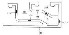
- the present invention is not limited to this, and a plurality of sensors are disposed and elastic. You may make it detect the distortion amount in several places of a film
- an elastic film 102 for forming a plurality of pressure chambers 101a to 101d is provided between the top ring 41, and a plurality of sensors 103a to 103d are provided at positions corresponding to the pressure chambers. It may be.
- the internal pressures of the pressure chambers 101a to 101d are made uniform by controlling the valves 104a to 104d connected to the fluid supply source 83 so that the distortion amounts detected by the sensors 103a to 103d are constant. Can be adjusted.
- the shape of the elastic membrane applied to the present invention is not particularly limited.
- the sensors 113 to 117 may be arranged.
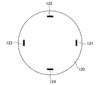
- a plurality of sensors 121 to 124 may be arranged along the circumferential direction of the elastic film 120. Thereby, the distribution of elongation of the elastic film can be detected accurately.
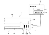
- the present invention is not limited to this, and the sensor may be disposed on the retainer ring as shown in FIG. In FIG. 14, three sensors 131 to 133 are embedded in the retainer ring 130, and these sensors 131 to 133 detect the amount of strain received during the polishing process, similar to those used in the above-described embodiment. In addition, various information is transmitted to and received from the control device 15 via the detector 91.
- the plurality of sensors 131 to 133 are embedded in the retainer ring 130 according to the present embodiment, distortions detected by the plurality of sensors 131 to 133 when performing polishing using a dummy wafer. The amount can be monitored. Then, as shown in FIG. 15 (b), when the displacement of the distortion amounts (arrows in the figure) from these sensors 131 to 133 falls within a predetermined value, the test polishing with the dummy wafer is terminated, whereby the retainer Break-in processing can be performed reliably regardless of the difference in ring material and polishing conditions.
- the break-in process is controlled using a plurality of strain sensors provided in the retainer ring 130, but the present invention is not limited to this, and for example, a plurality of strain sensors.
- the substrate processing conditions such as the pressure in the elastic film may be changed as appropriate according to the variation in strain information.
- control device acquires information on the type of consumables such as elastic membranes or retainer rings, the replacement time, and the number of strain measurements, and on the basis of these information, the maintenance date and time (or the time until maintenance) of the substrate processing apparatus is acquired. Time) may be calculated and displayed. As a result, the operator can appropriately grasp the maintenance timing of the apparatus.
- control device may be configured to automatically order consumables such as an elastic membrane and a retainer ring when the calculated maintenance date and time approaches (for example, several days ago). Sometimes a consumable can be reliably prepared.
- a program that causes the control device to calculate the maintenance date and place an order for consumables may be stored in advance in the memory of the control device, or may be installed later via the Internet or the like. good.
- a communication function may be provided in the control device so that it can be connected to an external server via a network, and various information such as the operating status of the device, strain data, and polishing environment information may be transmitted to the external server.
- the external server may be configured so that the control pattern of the substrate processing apparatus is standardized and automatically operated while adjusting polishing conditions such as polishing pressure based on various data received from the control apparatus. Further, it may be configured to be connectable to other substrate processing via a network, and may share various information such as the operating status of the apparatus, strain data, and polishing environment information.
- abnormality detection of the substrate processing apparatus and consumables used in the substrate processing apparatus is performed based on various types of information sent from the substrate processing apparatus and various types of information from other substrate processing apparatuses. Further, life prediction and determination may be performed, and abnormality detection and life display may be performed. Furthermore, it is possible to perform control for stabilizing the performance of the substrate processing apparatus in the external server.
- distortion data and other output data sent from the sensor are automatically learned by extracting feature values and the control pattern is automatically standardized to predict, judge, and display abnormalities and lifetimes. You may make it do.
- the format may be standardized in communication, device interface, etc., and the device / device management may be performed using information communication between the device / device.
- the elongation distribution of the consumables is measured using a strain sensor.
- the type of sensor is not limited, and for example, the temperature distribution may be measured using a temperature sensor, or The pressure distribution may be measured using a pressure sensor. Further, a plurality of types of sensors may be used in combination.
- the substrate polishing apparatus for polishing the wafer W has been described as an example.
- the present invention is not limited to this, and for example, as a consumable in a substrate cleaning apparatus that cleans a substrate after polishing processing.
Abstract
A substrate processing device having a substrate polishing unit 40 provided with a polishing pad for polishing a wafer W, and a top ring 41 for holding the wafer and pushing the wafer toward the polishing pad. An elastic film 80 that holds a surface of the wafer W on the side opposite from the polishing surface is attached as an expendable component to the top ring 41. A plurality of distortion sensors 85, 86 that measure distortion occurring in the elastic film 80 during polishing are provided to the elastic film 80, and data of a distortion amount is read out to a control device 15 by detection units 90, 91. The control device 15 sets process conditions such as a polishing recipe for the wafer W on the basis of distortion information of the elastic film 80 measured by the distortion sensors.
Description
本発明は、半導体ウェハ等の基板の表面を処理する基板処理装置に関する。
The present invention relates to a substrate processing apparatus for processing the surface of a substrate such as a semiconductor wafer.
半導体ウェハ等の基板を研磨する基板研磨装置や、基板表面を洗浄する基板洗浄装置といった基板処理装置においては、研磨パッド等の消耗品が用いられている。これら消耗品の種類や特性に関する情報を記録したRFタグを、消耗品に取り付けておき、装置の使用時にこれら情報を読み取るようにした研磨装置が知られている(特許文献1参照)。
In substrate processing apparatuses such as a substrate polishing apparatus for polishing a substrate such as a semiconductor wafer and a substrate cleaning apparatus for cleaning a substrate surface, consumables such as a polishing pad are used. A polishing apparatus is known in which an RF tag that records information on the type and characteristics of these consumables is attached to the consumables, and the information is read when the apparatus is used (see Patent Document 1).
また、特許文献2には、研磨パッド等の消耗品を装置から取り外すときにRFタグのメモリ情報を消去して情報の漏洩を防止するとともに、異常監視部により異常の発生が検出された場合には異常情報をRFタグに書き込むようにした研磨装置が開示されている。
Japanese Patent Laid-Open No. 2004-228688 discloses a case where the memory information of the RF tag is erased when a consumable such as a polishing pad is removed from the apparatus to prevent information leakage, and when an abnormality is detected by the abnormality monitoring unit. Discloses a polishing apparatus in which abnormal information is written in an RF tag.
半導体デバイスの高集積化・高密度化に伴い、回路の配線がますます微細化し、多層配線の層数も増加しており、製造工程における半導体デバイス表面の平坦化がますます重要になっている。基盤処理装置に用いられる消耗品は、基板処理を繰り返すことで摩耗や変形しやすく、それにより研磨圧力等の基板処理条件が変動してしまうと、研磨処理後の基板の膜厚に揺らぎが生じたり、場合によっては研磨不良等のトラブルが発生するおそれがある。よって、基板処理の条件を一定とするためには、基板処理に用いられる消耗品の状況をより正確に検出することが望ましい。
With higher integration and higher density of semiconductor devices, circuit wiring is becoming increasingly finer and the number of layers of multilayer wiring is increasing, and planarization of the surface of semiconductor devices in the manufacturing process is becoming increasingly important. . Consumables used in substrate processing equipment are subject to wear and deformation due to repeated substrate processing, and fluctuations in substrate processing conditions such as polishing pressure can cause fluctuations in the thickness of the substrate after polishing. In some cases, problems such as poor polishing may occur. Therefore, in order to make the substrate processing conditions constant, it is desirable to more accurately detect the status of consumables used for substrate processing.
本発明は、上記に鑑みなされたものであり、基板処理に用いられる消耗品の状況をより正確に検出することで、基板処理の条件を一定とすることが可能な基板処理装置を提供することを目的とする。
The present invention has been made in view of the above, and provides a substrate processing apparatus capable of making substrate processing conditions constant by more accurately detecting the status of consumables used for substrate processing. With the goal.
本発明の一態様は、基板を処理する基板処理装置であって、前記基板処理装置において使用される消耗品と、前記消耗品に取り付けられ、前記消耗品の物理量を測定するとともに、前記物理量を記憶する記憶部及び通信部を備える少なくとも1つのセンサと、前記消耗品の近傍に設けられ、前記消耗品に取り付けられた前記センサとの間で情報の読み書きを行う検出器と、前記検出器と接続され、前記センサから読み出された前記消耗品の物理量に基づき、基板処理装置における処理条件を設定する制御装置とを備えることを特徴とする。
One aspect of the present invention is a substrate processing apparatus that processes a substrate, the consumable used in the substrate processing apparatus, and a physical quantity of the consumable that is attached to the consumable and measures the physical quantity. At least one sensor provided with a storage unit and a communication unit for storing; a detector provided in the vicinity of the consumables; and a sensor for reading and writing information between the sensors attached to the consumables; and the detector And a control device that sets processing conditions in the substrate processing apparatus based on a physical quantity of the consumables connected and read from the sensor.
本発明にかかる基板処理装置において、前記記憶部には前記センサの識別情報が記憶されており、前記制御装置は、前記センサから読み出された前記識別情報に基づいて、前記消耗品が取り付けられた前記基板処理装置の駆動の可否を決定する要にすることが好ましい。また、前記基板処理装置に異常が発生したときに、前記基板の処理条件に関する情報を前記センサ内の記憶部に記録するようにすることが好ましい。
In the substrate processing apparatus according to the present invention, identification information of the sensor is stored in the storage unit, and the consumable is attached to the control device based on the identification information read from the sensor. Further, it is preferable to determine whether or not the substrate processing apparatus can be driven. In addition, it is preferable that information regarding the processing conditions of the substrate is recorded in a storage unit in the sensor when an abnormality occurs in the substrate processing apparatus.
本発明の一実施形態に係る基板処理装置は、前記基板を研磨する研磨パッドと、前記基板を保持して前記研磨パッドに押しつけるための基板保持部とを備えた基板研磨装置であって、前記消耗品は、前記基板保持部に取り付けられて前記基板の研磨面とは反対側の面を保持する弾性膜であり、前記センサは前記弾性膜の歪みを計測する歪みセンサであり、前記制御装置は、前記歪みセンサで計測された前記弾性膜の歪み情報に基づき、基板処理装置における処理条件を設定することができる。
A substrate processing apparatus according to an embodiment of the present invention is a substrate polishing apparatus comprising: a polishing pad for polishing the substrate; and a substrate holding unit for holding the substrate and pressing the substrate against the polishing pad. The consumable is an elastic film that is attached to the substrate holding unit and holds a surface opposite to the polishing surface of the substrate, and the sensor is a strain sensor that measures strain of the elastic film, and the control device Can set processing conditions in the substrate processing apparatus based on the strain information of the elastic film measured by the strain sensor.
上記の基板研磨装置において、前記弾性膜と前記基板保持部との間に少なくとも一つの圧力室が形成されており、前記制御装置は、前記歪みセンサで計測された前記弾性膜の歪み情報に基づき、前記圧力室内の圧力を調整することが好ましい。弾性膜の製造ばらつきや原料ロットの物性ばらつきにより、同じ内圧で加圧しても弾性膜が同じように膨らまず、基板に加わる圧力が弾性膜の個体によって変わってしまうことがあるところ、上記のように圧力を調整することで、このばらつきをキャンセルすることができる。
In the substrate polishing apparatus, at least one pressure chamber is formed between the elastic film and the substrate holding unit, and the control device is based on strain information of the elastic film measured by the strain sensor. The pressure in the pressure chamber is preferably adjusted. Due to variations in production of elastic membranes and variations in physical properties of raw material lots, even if pressure is applied at the same internal pressure, the elastic membrane does not swell in the same way, and the pressure applied to the substrate may vary depending on the individual elastic membrane. This variation can be canceled by adjusting the pressure.
上記の基板研磨装置において、前記基板が保持された前記弾性膜の側壁に対して気体又は液体を噴射することで、研磨済みの前記基板を前記弾性膜から剥離させるための噴射部を備えており、前記制御装置は、前記噴射部からの気体又は液体が、前記弾性膜と前記基板との境界に噴射されるように、前記弾性膜の歪み情報に基づき前記圧力室内の圧力を調整することが好ましい。これにより、気体又は液体を効果的に前記弾性膜と前記基板との境界に噴射することができる。
In the above-described substrate polishing apparatus, the substrate polishing apparatus includes an injection unit for separating the polished substrate from the elastic film by injecting gas or liquid onto the side wall of the elastic film holding the substrate. The control device may adjust the pressure in the pressure chamber based on strain information of the elastic film so that gas or liquid from the injection unit is injected to a boundary between the elastic film and the substrate. preferable. Thereby, gas or liquid can be effectively injected to the boundary between the elastic film and the substrate.
また、前記噴射部は、前記気体又は液体の噴射角度が調整可能とされており、前記弾性膜と前記基板との境界部分を撮像する撮像部と、前記撮像手段で得られた画像より、前記境界部分の位置を検出する画像処理部と、前記画像処理部で検出された前記境界部分の位置に基づき、前記噴射部による噴射角度を決定して、前記噴射角度を調節する噴射角度調節部とを備えることが好ましい。
In addition, the jetting unit is capable of adjusting the jetting angle of the gas or liquid, and from the image obtained by the imaging unit that images the boundary portion between the elastic film and the substrate, An image processing unit for detecting a position of the boundary part; and an injection angle adjusting unit for determining an injection angle by the injection unit based on the position of the boundary part detected by the image processing unit and adjusting the injection angle; It is preferable to provide.
本発明の一実施形態に係る基板処理装置は、前記基板を研磨する研磨パッドと、前記基板を保持して前記研磨パッドに押しつけるための基板保持部とを備えた基板研磨装置であって、前記消耗品は、前記基板の外周を支持するリテーナリングであり、前記センサは前記リテーナリングの歪みを計測する複数の歪みセンサであり、前記制御装置は、前記複数の歪みセンサで検出された歪み量のばらつきが所定値以内であるかを検出することが好ましい。
A substrate processing apparatus according to an embodiment of the present invention is a substrate polishing apparatus comprising: a polishing pad for polishing the substrate; and a substrate holding unit for holding the substrate and pressing the substrate against the polishing pad. The consumable is a retainer ring that supports the outer periphery of the substrate, the sensor is a plurality of strain sensors that measure the strain of the retainer ring, and the control device detects the amount of strain detected by the plurality of strain sensors. It is preferable to detect whether or not the variation of the difference is within a predetermined value.
基板研磨装置の使用初期、あるいはリテーナリングを交換した直後は、リテーナリングの接地面の形状が研磨パッドの研磨面に倣っておらず、リテーナリングの研磨面への当たり方にばらつきが生じ、リテーナリングの位置によってリテーナリングの垂直方向にかかる圧縮力にもばらつきが生じる。このため、リテーナリングに設けられた複数の歪みセンサで検出される歪み量にもばらつきが生じるが、リテーナリングのブレークインが完了すると、リテーナリング接地面の形状がパッドの研磨面に倣うことから、これら複数の歪みセンサで検出される歪み量のばらつきが小さくなる。これにより、リテーナリングのブレークインが完了したことを効果的に検出することができる。
In the initial stage of use of the substrate polishing apparatus, or immediately after replacing the retainer ring, the shape of the grounding surface of the retainer ring does not follow the polishing surface of the polishing pad, resulting in variations in how the retainer ring contacts the polishing surface. The compressive force applied in the vertical direction of the retainer ring also varies depending on the position of the ring. For this reason, the amount of strain detected by a plurality of strain sensors provided in the retainer ring also varies, but when the break-in of the retainer ring is completed, the shape of the retainer ring grounding surface follows the polishing surface of the pad. The variation in the amount of distortion detected by the plurality of strain sensors is reduced. Thereby, it is possible to effectively detect that the break-in of the retainer ring has been completed.
本発明の一実施形態に係る基板処理装置は、前記基板を研磨する研磨パッドと、前記基板を保持して前記研磨パッドに押しつけるための基板保持部とを備えた基板研磨装置であって、前記消耗品は、前記基板の外周を支持するリテーナリングであり、前記センサは前記リテーナリングの歪みを計測する複数の歪みセンサであり、前記制御装置は、前記複数の歪みセンサで検出された歪み量の分布に応じて、前記基板の処理条件を変更することを特徴とするものである。
A substrate processing apparatus according to an embodiment of the present invention is a substrate polishing apparatus comprising: a polishing pad for polishing the substrate; and a substrate holding unit for holding the substrate and pressing the substrate against the polishing pad. The consumable is a retainer ring that supports the outer periphery of the substrate, the sensor is a plurality of strain sensors that measure the strain of the retainer ring, and the control device detects the amount of strain detected by the plurality of strain sensors. The processing conditions of the substrate are changed in accordance with the distribution of.
本発明によれば、基板処理装置において使用される消耗品の物理量を測定するセンサを当該消耗品に取り付けるとともに、当該センサから読み出された消耗品の物理量に基づき、基板処理装置における処理条件を設定するようにしたから、基板処理に用いられる消耗品の状況をより正確に検出でき、基板処理の条件を一定とすることが可能となる。
According to the present invention, a sensor for measuring the physical quantity of a consumable used in the substrate processing apparatus is attached to the consumable, and the processing conditions in the substrate processing apparatus are determined based on the physical quantity of the consumable read out from the sensor. Since it is set, the status of the consumables used for the substrate processing can be detected more accurately, and the substrate processing conditions can be made constant.
以下、本発明の一実施形態に係る基板処理装置について、図面を参照して説明する。なお、同一または相当する構成要素には、同一の符号を付して重複した説明を省略する。
Hereinafter, a substrate processing apparatus according to an embodiment of the present invention will be described with reference to the drawings. In addition, the same code | symbol is attached | subjected to the component which is the same or it corresponds, and the overlapping description is abbreviate | omitted.
図1は、基板処理装置の全体構成を示す平面図である。基板処理装置10は、ロード/アンロード部12、研磨部13と、洗浄部14とに区画されており、これらは矩形状のハウジング11の内部に設けられている。また、基板処理装置10は、基板搬送、研磨、洗浄等の処理の動作制御を行う制御装置15を有している。
FIG. 1 is a plan view showing the overall configuration of the substrate processing apparatus. The substrate processing apparatus 10 is divided into a load / unload unit 12, a polishing unit 13, and a cleaning unit 14, which are provided inside a rectangular housing 11. The substrate processing apparatus 10 also includes a control device 15 that controls operation of processing such as substrate transport, polishing, and cleaning.
ロード/アンロード部12は、複数のフロントロード部20と、走行機構21と、2台の搬送ロボット22を備えている。フロントロード部20には、多数の基板(基板)をストックする基板カセットが載置される。搬送ロボット22は、上下に2つのハンドを備えており、走行機構21上を移動することで、フロントロード部20内の基板カセットから基板Wを取り出して研磨部13へ送るとともに、洗浄部14から送られる処理済みの基板を基板カセットに戻す動作を行う。
The load / unload unit 12 includes a plurality of front load units 20, a travel mechanism 21, and two transfer robots 22. A substrate cassette that stocks a large number of substrates (substrates) is placed on the front load unit 20. The transfer robot 22 has two hands up and down, and moves on the traveling mechanism 21 to take out the substrate W from the substrate cassette in the front load unit 20 and send it to the polishing unit 13, and from the cleaning unit 14. An operation of returning the processed substrate to be sent back to the substrate cassette is performed.
研磨部13は、基板の研磨(平坦化処理)を行う領域であり、複数の研磨ユニット13A~13Dが設けられ、基板処理装置の長手方向に沿って配列されている。個々の研磨ユニットは、研磨テーブル上の基板Wを研磨パッドに押圧しながら研磨するためのトップリングと、研磨パッドに研磨液やドレッシング液を供給する研磨液供給ノズルと、研磨パッドの研磨面のドレッシングを行うドレッサと、液体と気体の混合流体または霧状の液体を研磨面に噴射して研磨面に残留する研磨屑や砥粒を洗い流すアトマイザを備えている。
The polishing unit 13 is an area for polishing (planarizing) the substrate, and is provided with a plurality of polishing units 13A to 13D, which are arranged along the longitudinal direction of the substrate processing apparatus. Each polishing unit includes a top ring for polishing the substrate W on the polishing table against the polishing pad, a polishing liquid supply nozzle for supplying a polishing liquid and a dressing liquid to the polishing pad, and a polishing surface of the polishing pad. A dresser that performs dressing and an atomizer that sprays a mixed fluid of liquid and gas or a mist-like liquid onto the polishing surface to wash away polishing debris and abrasive grains remaining on the polishing surface are provided.
研磨部13と洗浄部14との間には、基板Wを搬送する搬送機構として、第1,第2リニアトランスポータ16,17が設けられている。第1リニアトランスポータ16は、ロード/アンロード部12から基板Wを受け取る第1位置、研磨ユニット13A,13Bとの間で基板Wの受け渡しを行う第2,第3位置、第2リニアトランスポータ17へ基板Wを受け渡すための第4位置との間で移動自在とされている。
As the transport mechanism for transporting the substrate W, first and second linear transporters 16 and 17 are provided between the polishing unit 13 and the cleaning unit 14. The first linear transporter 16 has a first position for receiving the substrate W from the load / unload unit 12, second and third positions for transferring the substrate W between the polishing units 13A and 13B, and a second linear transporter. It is possible to move between a fourth position for delivering the substrate W to 17.
第2リニアトランスポータ17は、第1リニアトランスポータ16から基板Wを受け取るための第5位置、研磨ユニット13C,13Dとの間で基板Wの受け渡しを行う第6,第7位置との間で移動自在とされている。これらトランスポータ16,17の間には、基板Wを洗浄部14へ送るためのスイングトランスポータ23が備えられている。
The second linear transporter 17 is between the fifth position for receiving the substrate W from the first linear transporter 16 and the sixth and seventh positions for transferring the substrate W between the polishing units 13C and 13D. It is supposed to be movable. A swing transporter 23 for sending the substrate W to the cleaning unit 14 is provided between the transporters 16 and 17.
洗浄部14は、第1基板洗浄装置30、第2基板洗浄装置31、基板乾燥装置32と、これら装置間で基板の受け渡しを行うための搬送ロボット33,34を備えている。研磨ユニットで研磨処理が施された基板Wは、第1基板洗浄装置30で洗浄(一次洗浄)され、次いで第2基板洗浄装置31で更に洗浄(仕上げ洗浄)される。洗浄後の基板は、第2基板洗浄装置31から基板乾燥装置32に搬入されてスピン乾燥が施される。乾燥後の基板Wは、ロード/アンロード部12に戻される。
The cleaning unit 14 includes a first substrate cleaning device 30, a second substrate cleaning device 31, a substrate drying device 32, and transfer robots 33 and 34 for transferring substrates between these devices. The substrate W that has been subjected to the polishing process by the polishing unit is cleaned (primary cleaning) by the first substrate cleaning device 30 and then further cleaned (finish cleaning) by the second substrate cleaning device 31. The cleaned substrate is transferred from the second substrate cleaning device 31 to the substrate drying device 32 and subjected to spin drying. The dried substrate W is returned to the load / unload unit 12.
図2は研磨ユニットの構成を概略的に示す斜視図であり、図3は研磨ユニットの構成を概略的に示す側面図である。研磨ユニット40は、ウェハ(基板)Wを保持して回転させるトップリング(基板保持装置)41と、研磨パッド42を指示する研磨テーブル43と、研磨パッド42にスラリー(研磨液)を供給する研磨液供給ノズル45と、ウェハWの膜厚に応じて変化する信号を取得する膜厚センサ47とを備えている。
FIG. 2 is a perspective view schematically showing the configuration of the polishing unit, and FIG. 3 is a side view schematically showing the configuration of the polishing unit. The polishing unit 40 holds a wafer (substrate) W and rotates it, a top ring (substrate holding device) 41, a polishing table 43 that instructs the polishing pad 42, and polishing that supplies slurry (polishing liquid) to the polishing pad 42. A liquid supply nozzle 45 and a film thickness sensor 47 that acquires a signal that changes according to the film thickness of the wafer W are provided.
トップリング41は、その下面に真空吸着によりウェハWを保持できるように構成されている。トップリング41と研磨テーブル43は、矢印で示す方向に回転し、この状態でトップリング41は、ウェハWを研磨パッド42の上側の研磨面42aに押しつける。研磨液供給ノズル45から研磨パッド42上に供給される研磨液の存在下で、ウェハWは研磨パッド42に摺接されて研磨される。
The top ring 41 is configured to hold the wafer W by vacuum suction on the lower surface thereof. The top ring 41 and the polishing table 43 rotate in the direction indicated by the arrow. In this state, the top ring 41 presses the wafer W against the upper polishing surface 42 a of the polishing pad 42. In the presence of the polishing liquid supplied from the polishing liquid supply nozzle 45 onto the polishing pad 42, the wafer W is slid in contact with the polishing pad 42 and polished.
膜厚センサ47は、例えば光学式センサや渦電流センサが用いられ、研磨テーブル43の内部に設置されている。ウェハWの研磨中、膜厚センサ47は研磨テーブル43とともに回転し、ウェハWの表面を横切る際に膜厚に応じた膜厚信号を取得する。膜厚センサ47からの膜厚信号は制御装置15に送信され、膜厚装置15は膜厚信号で示されるウェハWの膜厚が設定値に達したときに、ウェハWの研磨を終了する。
The film thickness sensor 47 is, for example, an optical sensor or an eddy current sensor, and is installed inside the polishing table 43. During polishing of the wafer W, the film thickness sensor 47 rotates with the polishing table 43 and acquires a film thickness signal corresponding to the film thickness when crossing the surface of the wafer W. The film thickness signal from the film thickness sensor 47 is transmitted to the control device 15, and the film thickness device 15 ends the polishing of the wafer W when the film thickness of the wafer W indicated by the film thickness signal reaches a set value.
図3において、トップリング41は、ウェハWを研磨面42aに対して押圧するヘッド本体48と、ウェハWの外周部を支持してウェハWがトップリング41から飛び出すのを防止するリテーナリング49とを備えている。トップリング41は、トップリングシャフト51に接続されており、トップリングシャフト51の上端には、ロータリージョイント55が取り付けられている。トップリングシャフト51は、上下動機構57によりヘッドアーム56に対して上下動するように構成されており、ヘッドアーム26に対してトップリング51の全体を昇降させ位置決めするようになっている。
In FIG. 3, the top ring 41 includes a head main body 48 that presses the wafer W against the polishing surface 42 a, and a retainer ring 49 that supports the outer periphery of the wafer W and prevents the wafer W from jumping out of the top ring 41. It has. The top ring 41 is connected to the top ring shaft 51, and a rotary joint 55 is attached to the upper end of the top ring shaft 51. The top ring shaft 51 is configured to move up and down with respect to the head arm 56 by a vertical movement mechanism 57, and is configured to move the entire top ring 51 up and down relative to the head arm 26.
トップリングシャフト51およびトップリング41を上下動させる上下動機構67は、軸受66を介してトップリングシャフト51を回転可能に支持するブリッジ68と、ブリッジ68に取り付けられたボールねじ72と、支柱70により支持された支持台69と、支持台69上に設けられたサーボモータ78とを備えている。サーボモータ78を支持する支持台69は、支柱70を介してヘッドアーム56に固定されている。
A vertical movement mechanism 67 that moves the top ring shaft 51 and the top ring 41 up and down includes a bridge 68 that rotatably supports the top ring shaft 51 via a bearing 66, a ball screw 72 attached to the bridge 68, and a column 70. And a servo motor 78 provided on the support base 69. A support base 69 that supports the servo motor 78 is fixed to the head arm 56 via a column 70.
ボールねじ72は、サーボモータ78に連結されたねじ軸72aと、このねじ軸42aが螺合するナット72bとを備えている。トップリングシャフト51は、ブリッジ68と一体となって上下動するようになっている。したがって、サーボモータ78を駆動すると、ボールねじ78を介してブリッジ68が上下動し、これによりトップリングシャフト51およびトップリング41が上下動する。
The ball screw 72 includes a screw shaft 72a connected to the servo motor 78, and a nut 72b into which the screw shaft 42a is screwed. The top ring shaft 51 moves up and down integrally with the bridge 68. Therefore, when the servo motor 78 is driven, the bridge 68 moves up and down via the ball screw 78, and thereby the top ring shaft 51 and the top ring 41 move up and down.
トップリングシャフト51はキー(図示せず)を介して回転筒52に連結されている。この回転筒52はその外周部にタイミングプーリ54を備えている。ヘッドアーム56にはヘッドモータ58が固定されており、上記タイミングプーリ54は、タイミングベルト59を介してヘッドモータ58に設けられたタイミングプーリ60に接続されている。ヘッドモータ58を回転駆動することによってタイミングプーリ60、タイミングベルト59、およびタイミングプーリ54を介して回転筒52およびトップリングシャフト51が一体に回転し、トップリング11が回転する。ヘッドアーム56は、フレーム(図示せず)に回転可能に支持されたアームシャフト61によって支持されている。研磨装置を構成するヘッドモータ58、サーボモータ78をはじめとする装置内の各部品は、制御装置15によってその動作が制御されている。
The top ring shaft 51 is connected to the rotary cylinder 52 via a key (not shown). The rotary cylinder 52 includes a timing pulley 54 on the outer periphery thereof. A head motor 58 is fixed to the head arm 56, and the timing pulley 54 is connected to a timing pulley 60 provided in the head motor 58 via a timing belt 59. By rotating the head motor 58, the rotary cylinder 52 and the top ring shaft 51 rotate together via the timing pulley 60, the timing belt 59, and the timing pulley 54, and the top ring 11 rotates. The head arm 56 is supported by an arm shaft 61 that is rotatably supported by a frame (not shown). The operation of each component in the apparatus including the head motor 58 and the servo motor 78 constituting the polishing apparatus is controlled by the controller 15.
ヘッドアーム56はアームシャフト61を中心として旋回可能に構成されており、下面にウェハWを保持したトップリング41は、ヘッドアーム56の旋回によりウェハWの受取位置から研磨テーブル52の上方の研磨位置に移動される。トップリング41および研磨テーブル42をそれぞれ回転させ、研磨液供給ノズル45から研磨パッド42上に研磨液を供給する。この状態で、トップリング41を所定の位置(高さ)まで下降させ、この所定の位置でウェハWを研磨パッド42の研磨面42aに押圧することで、ウェハWは研磨面42aに摺接されてその表面が研磨される。
The head arm 56 is configured to be pivotable about the arm shaft 61, and the top ring 41 holding the wafer W on the lower surface thereof is a polishing position above the polishing table 52 from the receiving position of the wafer W by the turning of the head arm 56. Moved to. The top ring 41 and the polishing table 42 are rotated, and the polishing liquid is supplied onto the polishing pad 42 from the polishing liquid supply nozzle 45. In this state, the top ring 41 is lowered to a predetermined position (height), and the wafer W is pressed against the polishing surface 42a of the polishing pad 42 at this predetermined position, so that the wafer W is brought into sliding contact with the polishing surface 42a. The surface is polished.
図4において、トップリング41を構成するトップリング本体48およびリテーナリング49は、トップリングシャフト51の回転により一体に回転するように構成されている。トップリングの下側には、ウェハWの裏面に当接する弾性膜(メンブレン)80が取り付けられており、弾性膜80の下面が基板保持面を構成する。弾性膜80は、鉛直方向に延びる環状の隔壁80aを有しており、これにより弾性膜80とトップリング本体48との間に圧力室81が形成される。
4, the top ring main body 48 and the retainer ring 49 constituting the top ring 41 are configured to rotate integrally with the rotation of the top ring shaft 51. An elastic film (membrane) 80 that is in contact with the back surface of the wafer W is attached to the lower side of the top ring, and the lower surface of the elastic film 80 forms a substrate holding surface. The elastic membrane 80 has an annular partition wall 80 a extending in the vertical direction, whereby a pressure chamber 81 is formed between the elastic membrane 80 and the top ring body 48.
この圧力室81には、バルブ82を介して流体供給源83に接続されており、この流体供給源83から加圧流体(ガス)が供給されるようになっている。また、バルブ82には、制御装置15が接続されており、これにより圧力室81内の圧力を調整することができ、圧力室82内に負圧を形成することも可能となっている。また、圧力室81は大気開放機構(図示せず)に接続されており、圧力室81を大気開放することも可能である。
The pressure chamber 81 is connected to a fluid supply source 83 via a valve 82, and pressurized fluid (gas) is supplied from the fluid supply source 83. Further, the control device 15 is connected to the valve 82, whereby the pressure in the pressure chamber 81 can be adjusted, and a negative pressure can be formed in the pressure chamber 82. Further, the pressure chamber 81 is connected to an atmosphere release mechanism (not shown), and the pressure chamber 81 can be opened to the atmosphere.
弾性膜80は、内側の圧力室81に対応する位置に通孔(図示せず)を有しており、この通孔に負圧を形成することにより、弾性膜80の基板保持面上でウェハWを保持できるようになっている。弾性膜80は、例えばエチレンプロピレンゴム(EPDM)、ポリウレタンゴム、シリコーンゴムといった、強度および耐久性に優れたゴム材によって形成されている。
The elastic film 80 has a through hole (not shown) at a position corresponding to the inner pressure chamber 81. By forming a negative pressure in the through hole, the wafer is formed on the substrate holding surface of the elastic film 80. W can be held. The elastic film 80 is formed of a rubber material having excellent strength and durability, such as ethylene propylene rubber (EPDM), polyurethane rubber, and silicone rubber.
リテーナリング49は、トップリング本体48及び弾性膜55を囲むように配置されている。このリテーナリング49は、研磨パッド42の研磨面42aに接触するリング状の部材であり、トップリング本体48に保持されるウェハWの外周縁を囲むように配置されており、研磨中のウェハWがトップリング41から飛び出さないようにウェハWの外周縁を支持している。
The retainer ring 49 is disposed so as to surround the top ring main body 48 and the elastic film 55. The retainer ring 49 is a ring-shaped member that comes into contact with the polishing surface 42a of the polishing pad 42, and is disposed so as to surround the outer peripheral edge of the wafer W held by the top ring main body 48. Supports the outer peripheral edge of the wafer W so as not to jump out of the top ring 41.
リテーナリング49の上面には、図示しない環状のリテーナリング押圧機構に連結されており、リテーナリング49の上面の全体に均一な下向きの荷重を与える。これによりリテーナリング49の下面を研磨パッド42の研磨面42aに対して押圧する。
The upper surface of the retainer ring 49 is connected to an annular retainer ring pressing mechanism (not shown), and a uniform downward load is applied to the entire upper surface of the retainer ring 49. As a result, the lower surface of the retainer ring 49 is pressed against the polishing surface 42 a of the polishing pad 42.
弾性膜80には、通信機能を備えたセンサ85及び86が設けられている。一方のセンサ85は、ウェハWと接する部分の近傍に設けられており、他方のセンサ86は弾性膜80の側壁80aに取り付けられている。本実施形態において、センサ85は弾性膜80の内部に埋め込まれるようにして設けられているが、ウェハWに接触しない限り、配置する位置に特段の限定はなく、例えば、弾性膜80のウェハWと接触する側の反対面(図4の上方の面)に配置しても良い。
The elastic film 80 is provided with sensors 85 and 86 having a communication function. One sensor 85 is provided in the vicinity of the portion in contact with the wafer W, and the other sensor 86 is attached to the side wall 80 a of the elastic film 80. In this embodiment, the sensor 85 is provided so as to be embedded in the elastic film 80. However, as long as the sensor 85 is not in contact with the wafer W, the position of the sensor 85 is not particularly limited. You may arrange | position on the opposite surface (upper surface of FIG. 4) of the side which contacts.
図5に示すように、センサ85,86は、検出部87、メモリ88と通信部89とを備える。検出部87は、例えば歪みセンサであり、センサにかかる歪み量を検出して、歪み情報として出力する。なお、本発明において、センサは歪みセンサに限られることはなく、例えば温度センサ、加速度センサ、傾斜センサを用いることができる。
As shown in FIG. 5, the sensors 85 and 86 include a detection unit 87, a memory 88, and a communication unit 89. The detector 87 is, for example, a strain sensor, detects the amount of strain applied to the sensor, and outputs it as strain information. In the present invention, the sensor is not limited to a strain sensor, and for example, a temperature sensor, an acceleration sensor, or a tilt sensor can be used.
メモリ88には、所定のデータが予め記憶された読出し専用領域88aと、読み出し/書き込み可能な書込み可能領域88bとが設けられており、読出し専用領域88aには、消耗品である弾性膜80のパーツナンバー(部品ID)、シリアルナンバー、使用期限、出荷検査データ、製造データといった情報が保存されている。ここで、出荷検査データには、弾性膜のゴム物性検査データ、外形寸法データ、膨らみ測定データが含まれており、製造データには、プレス圧力、プレス温度、プレス時間、二次加硫温度、二次加硫時間といった加工条件のデータが含まれる。
The memory 88 is provided with a read-only area 88a in which predetermined data is stored in advance, and a writable / writable area 88b. The read-only area 88a contains a consumable elastic film 80. Information such as a part number (part ID), a serial number, an expiration date, shipment inspection data, and manufacturing data is stored. Here, the shipment inspection data includes rubber physical property inspection data, outer dimension data, and swell measurement data of the elastic membrane, and the manufacturing data includes press pressure, press temperature, press time, secondary vulcanization temperature, Data on processing conditions such as secondary vulcanization time are included.
また、書込み可能領域88bには、検出部87で検出された歪み情報のデータ、及びウェハ処理データが記録される。ここで、ウェハ処理データには、消耗品である弾性膜80が交換された後の基板処理装置の使用開始日、最終使用日、積算ウェハ処理枚数、積算処理時間の情報が含まれる。
Further, in the writable area 88b, distortion information data detected by the detection unit 87 and wafer processing data are recorded. Here, the wafer processing data includes information on the use start date, the last use date, the total number of wafers processed, and the total processing time of the substrate processing apparatus after the elastic film 80 as a consumable is replaced.
通信部89は、例えば無線通信モジュールであり、基板処理装置10に設けられた検出器90,91(図4参照)との間で、読出し専用領域88a及び書込み可能領域88bに記憶されたデータの読出し処理を行う。検出器90,91は、通信部89との間で無線通信が可能な通信モジュールであり、対応するセンサ85,86の近傍に位置する読取位置と、トップリング41の移動領域から退避する待機位置との間で移動可能とされており、基板処理装置10による基板処理が行われていないタイミングで読取位置に移動して、センサ85,86との間でデータの送受信を行う。
The communication unit 89 is, for example, a wireless communication module, and exchanges data stored in the read-only area 88a and the writable area 88b with the detectors 90 and 91 (see FIG. 4) provided in the substrate processing apparatus 10. Perform read processing. The detectors 90 and 91 are communication modules capable of wireless communication with the communication unit 89, and are a reading position located in the vicinity of the corresponding sensors 85 and 86, and a standby position for retreating from the moving area of the top ring 41. Between the sensors 85 and 86, and data is transmitted to and received from the sensors 85 and 86 at a timing when the substrate processing by the substrate processing apparatus 10 is not performed.
制御装置15は、検出器90、91と有線または無線により直接に接続されており、センサ85、86から読み出された各種データを記憶するメモリ93と、センサ85、86から読み出された出荷検査データ、製造データに基づき、基板処理の条件(レシピやマシン定数)を設定する条件設定部94が設けられている。また、制御装置15のメモリ93には、検出器90,91、条件設定部94を含む、基板処理装置10の各構成要素の動作を制御するためのプログラムが記憶されており、基板処理装置10の動作時に読み出されることで、基板処理装置10の動作を制御する。なお、制御装置15と検出器90,91とを、インターネットや他の通信装置を介して接続するようにしても良い。
The control device 15 is directly connected to the detectors 90 and 91 by wire or wirelessly, and has a memory 93 for storing various data read from the sensors 85 and 86, and a shipment read from the sensors 85 and 86. A condition setting unit 94 is provided for setting substrate processing conditions (recipes and machine constants) based on inspection data and manufacturing data. The memory 93 of the control device 15 stores a program for controlling the operation of each component of the substrate processing apparatus 10 including the detectors 90 and 91 and the condition setting unit 94. The operation of the substrate processing apparatus 10 is controlled by being read during the operation. In addition, you may make it connect the control apparatus 15 and the detectors 90 and 91 via the internet or another communication apparatus.
また、センサ85,86が取り付けられた弾性膜80を基板処理装置10に取り付けたとき、あるいは、基板研磨処理が行われていない所定のタイミングで、当該センサ85,86のゼロ点調整が行われる。制御装置15は、例えば、弾性膜80に負荷(圧力)をかけていない状態、あるいは所定の圧力をかけた状態でのセンサ85,86からの出力を検出し、そのときのセンサ出力をゼロ点として設定することができる。
In addition, when the elastic film 80 to which the sensors 85 and 86 are attached is attached to the substrate processing apparatus 10 or at a predetermined timing when the substrate polishing process is not performed, the zero points of the sensors 85 and 86 are adjusted. . For example, the control device 15 detects the output from the sensors 85 and 86 when no load (pressure) is applied to the elastic membrane 80 or when a predetermined pressure is applied, and the sensor output at that time is zero. Can be set as
図6は、センサ85,86が取り付けられた弾性膜80を、基板処理装置10に取り付けたときの照合処理の手順を示すフローチャートである。基板処理装置10の制御装置15では、装置本体に消耗品である弾性膜80が修理・交換等により取り付けられたことを検出すると(ステップS10)、検出器90,91の双方またはいずれかを駆動して、対応するセンサ85,86に記憶された部品ID(パーツナンバー)を読み出す(ステップS11)。
FIG. 6 is a flowchart showing a verification processing procedure when the elastic film 80 to which the sensors 85 and 86 are attached is attached to the substrate processing apparatus 10. When the controller 15 of the substrate processing apparatus 10 detects that the elastic film 80, which is a consumable, is attached to the apparatus main body by repair or replacement (step S10), it drives both or one of the detectors 90 and 91. Then, the component ID (part number) stored in the corresponding sensor 85, 86 is read (step S11).
制御装置15では、読み出された部品IDが、予め基板処理装置10内のメモリ93に記憶されている部品IDと一致しているかどうかを判定する(ステップS12)。そして、読み出された部品IDが、メモリ93に記憶されている部品IDのいずれにも一致しない場合(例えば、基板処理装置10に適合しない弾性膜が誤ってセットされた場合、非正規品がセットされた場合)には、制御装置15は、基板処理装置10にインターロックをかけ、当該弾性膜を用いた研磨ユニット40にて基板研磨処理を行うことができないようにする(ステップS13)。
The control device 15 determines whether or not the read component ID matches the component ID stored in advance in the memory 93 in the substrate processing apparatus 10 (step S12). When the read component ID does not match any of the component IDs stored in the memory 93 (for example, when an elastic film that does not match the substrate processing apparatus 10 is set by mistake, When set, the control device 15 interlocks the substrate processing apparatus 10 so that the substrate polishing process cannot be performed by the polishing unit 40 using the elastic film (step S13).
一方、読み出された部品IDが、メモリ93に記憶されている部品IDのいずれかと一致する場合には、制御装置15は、メモリ88に記憶されている弾性膜80の出荷検査データや製造データを読み出して、制御装置15内のメモリ93に保存する(ステップS14)。そして、制御装置15は、メモリ88から読み出された各種データに基づき、基板研磨のレシピや装置のマシン定数を設定する(ステップS15)。その後、制御装置15は、研磨ユニットを駆動してウェハWに対する研磨処理を開始する(ステップS16)。
On the other hand, if the read component ID matches any of the component IDs stored in the memory 93, the control device 15 sends the shipping inspection data and manufacturing data of the elastic film 80 stored in the memory 88. Is stored in the memory 93 in the control device 15 (step S14). The control device 15 sets a substrate polishing recipe and a machine constant of the device based on various data read from the memory 88 (step S15). Thereafter, the control device 15 drives the polishing unit to start the polishing process for the wafer W (step S16).
図7は、基板研磨処理の動作を示すフローチャートである。基板研磨処理が開始されると(ステップS20)、センサ85,86は、研磨中の所定時間毎に、弾性膜80に生じている歪み量を検出し(ステップS21)、歪み量データとしてメモリ88の書込み領域88bに記録する(ステップS22)。そして、制御装置15は、基板の研磨処理が終了したかどうかを判定し(ステップS23)、研磨処理が終了した場合には、検出器90,91を駆動して、弾性膜80のメモリ88に記憶された歪み量データを読み出し、制御装置15内のメモリ93に保存する(ステップS24)。
FIG. 7 is a flowchart showing the operation of the substrate polishing process. When the substrate polishing process is started (step S20), the sensors 85 and 86 detect the amount of strain generated in the elastic film 80 every predetermined time during polishing (step S21), and the memory 88 is stored as strain amount data. Is recorded in the writing area 88b (step S22). Then, the control device 15 determines whether or not the polishing process of the substrate is finished (step S23), and when the polishing process is finished, the detectors 90 and 91 are driven and stored in the memory 88 of the elastic film 80. The stored distortion amount data is read out and stored in the memory 93 in the control device 15 (step S24).
制御装置15は、読み出された歪み量データに基づき、次のウェハWを研磨処理する際に適用される研磨レシピを設定する(ステップS25)。例えば、読み出された歪み量データから、弾性膜80の伸び量を算出し、弾性膜80のセット時に読み出されていたゴム物性検査データ、外形寸法データ、膨らみ測定データを用いて補正することで、研磨レシピの設定を行うことができる。その後、制御装置15は、研磨ユニットを駆動してウェハWに対する研磨処理を開始する(ステップS26)。
The control device 15 sets a polishing recipe to be applied when polishing the next wafer W based on the read distortion amount data (step S25). For example, the elongation amount of the elastic film 80 is calculated from the read strain amount data, and is corrected using the rubber physical property inspection data, the external dimension data, and the bulge measurement data read when the elastic film 80 is set. Thus, the polishing recipe can be set. Thereafter, the control device 15 drives the polishing unit to start the polishing process for the wafer W (step S26).
図7のフローチャートでは、歪み量データから次のウェハWの研磨時に用いられる研磨レシピの設定を行うようにしているが、本発明はこれに限られることはなく、例えば、歪み量が設定値から変動した場合に、歪み量を当該設定値に近づけるようにバルブ82の開き量を調整して、圧力室81内の圧力を調整するようにしても良い。また、センサ85,86のメモリ88内に記録された歪み量データは、制御装置15に読み出される際に消去しても良く、これによりメモリ88内のデータ容量を抑えることができる。
In the flowchart of FIG. 7, the polishing recipe used at the time of polishing the next wafer W is set from the distortion amount data. However, the present invention is not limited to this, and for example, the distortion amount is determined from the set value. In the case of fluctuation, the pressure in the pressure chamber 81 may be adjusted by adjusting the opening amount of the valve 82 so that the distortion amount approaches the set value. Further, the distortion amount data recorded in the memory 88 of the sensors 85 and 86 may be erased when being read out by the control device 15, whereby the data capacity in the memory 88 can be suppressed.
図8は、基板処理装置10に、研磨性能不良(例えば、研磨レート異常、研磨プロファイル異常、ウェハ上のパターンの段差性能異常)、ウェハのスリップアウト、ウェハ割れといったトラブルが発生した場合の処理手順を示すフローチャートである。
FIG. 8 shows a processing procedure in the case where troubles such as poor polishing performance (for example, abnormal polishing rate, abnormal polishing profile, abnormal step performance of the pattern on the wafer), wafer slipout, and wafer cracking occur in the substrate processing apparatus 10. It is a flowchart which shows.
制御装置15は、研磨ユニットに何らかのトラブルが発生したことを検出すると(ステップS30)、現在実行中の研磨処理を直ちに終了して、基板処理装置の動作を停止する(ステップS31)。次に、制御装置15は、検出器90,91を駆動して、制御装置15内のメモリから、各種情報(例えば、装置本体でカウントしたウェハ処理枚数、処理時間、使用開始/終了日、マシン定数やレシピの情報)を、装置内のメモリ93から読み出して(ステップS32)、これを弾性膜80に取り付けられたセンサ85,86内のメモリ88に書き込む(ステップS33)。
When the controller 15 detects that some trouble has occurred in the polishing unit (step S30), it immediately ends the polishing process currently being executed and stops the operation of the substrate processing apparatus (step S31). Next, the control device 15 drives the detectors 90 and 91 to read various information (for example, the number of wafers processed, the processing time, the start / end date of use, the machine count) from the memory in the control device 15. Constants and recipe information) are read from the memory 93 in the apparatus (step S32), and are written in the memory 88 in the sensors 85 and 86 attached to the elastic film 80 (step S33).
その後、トップリング41のロックが解除されて、弾性膜80をトップリング41から取り外される。取り外された弾性膜80は、図示しないオフラインリーダーにセットされて、弾性膜80に取り付けられたセンサ85,86内のメモリ88より、ステップS33で書き込まれた各種情報及びメモリ88内に記録されていた、基板研磨処理中の歪み量データが読み出される(ステップS34)。これにより、読み出された各種情報及び歪み量データを解析することで、故障原因の診断を行うことができる(ステップS35)。なお、故障原因の診断の際に、取り出された弾性膜80のゴム物性、外形寸法、膨らみの検査を行うようにしても良い。
Thereafter, the lock of the top ring 41 is released, and the elastic film 80 is removed from the top ring 41. The removed elastic film 80 is set in an offline reader (not shown) and recorded in the memory 88 in the sensors 88 and 86 attached to the elastic film 80 in the various information written in step S33 and in the memory 88. In addition, distortion amount data during the substrate polishing process is read (step S34). As a result, the cause of the failure can be diagnosed by analyzing the various information and distortion amount data that have been read (step S35). Note that, when diagnosing the cause of the failure, the rubber properties, outer dimensions, and swelling of the extracted elastic film 80 may be inspected.
上記実施形態では、消耗品である弾性膜の取り付け時、基板研磨時及びトラブル発生時におけるセンサ85,86の動作について説明したが、本発明はこれに限られることはなく、例えば図9に示すように、研磨処理後のウェハWを弾性膜から離脱する際にも適用することができる。
In the above embodiment, the operation of the sensors 85 and 86 at the time of attaching the elastic film as a consumable, polishing the substrate, and at the time of trouble occurrence has been described. However, the present invention is not limited to this, for example, as shown in FIG. As described above, the present invention can also be applied when the wafer W after the polishing process is detached from the elastic film.
図9において、トップリング41の近傍には、制御装置15に接続されるガス噴射部100が配置されている。研磨処理直後のウェハWは弾性膜80に吸着されているため、そのままではウェハWを弾性膜80から離脱させることができない。そこで、ガス噴射部100は、研磨処理が終了した後の所定タイミングで、ウェハWと弾性膜80との接合部の近傍(弾性膜の側壁部分近傍の膨らんだ部分)に向けて、例えば不揮発性ガスを噴射する。これにより、研磨処理が終了したウェハWを弾性膜80から離脱させることができる。なお、ガスに代えて、液体(純水)を噴射するようにしても良い。
9, a gas injection unit 100 connected to the control device 15 is disposed in the vicinity of the top ring 41. Since the wafer W immediately after the polishing process is adsorbed by the elastic film 80, the wafer W cannot be detached from the elastic film 80 as it is. Therefore, the gas injection unit 100 is, for example, non-volatile toward the vicinity of the bonding portion between the wafer W and the elastic film 80 (the swollen portion near the side wall portion of the elastic film) at a predetermined timing after the polishing process is completed. Inject gas. As a result, the wafer W that has undergone the polishing process can be detached from the elastic film 80. Note that liquid (pure water) may be ejected instead of gas.
ここで、弾性膜80の膨らみ部分の位置(図中上下方向の位置)は、常に一定ではなく、弾性膜の製造条件、ゴム物性検査データ、外見寸法データ、基板処理枚数や処理時間、圧力室81の圧力等に応じて変動する。そして、ガス噴射部100からのガスが、弾性膜80と基板との境界からずれた位置に噴射されてしまう場合、研磨処理が終了したウェハWを弾性膜80から容易に離脱させることができなくなる。
Here, the position of the bulging portion of the elastic film 80 (the vertical position in the figure) is not always constant, and the elastic film manufacturing conditions, rubber physical property inspection data, appearance dimension data, number of processed substrates, processing time, pressure chamber It fluctuates according to the pressure of 81 or the like. When the gas from the gas injection unit 100 is injected to a position shifted from the boundary between the elastic film 80 and the substrate, the wafer W after the polishing process cannot be easily detached from the elastic film 80. .
そこで、研磨処理終了後、ウェハWを弾性膜から離脱する際に、センサ85,86にて歪み量を検出するとともに制御装置15においてこれらセンサで検出された歪み量が設定値に達したときに、バルブ82を駆動して流体供給源83からの流体供給をストップする。これにより、研磨処理終了後、ウェハWを弾性膜から離脱する際に、圧力室81の圧力が一定となり、弾性膜80の膨らみ部分の位置が一定となるため、ガス噴射部100からのガスを弾性膜80とウェハWとの境界に確実に当てることができる。
Therefore, when the wafer W is detached from the elastic film after the polishing process is completed, the amount of distortion is detected by the sensors 85 and 86 and the amount of distortion detected by these sensors in the control device 15 reaches a set value. Then, the valve 82 is driven to stop the fluid supply from the fluid supply source 83. Thereby, when the wafer W is detached from the elastic film after the polishing process is finished, the pressure in the pressure chamber 81 becomes constant and the position of the bulging portion of the elastic film 80 becomes constant. It can be reliably applied to the boundary between the elastic film 80 and the wafer W.
図10は、研磨処理後のウェハWを弾性膜から離脱させる構成の別の例を示したものである。図10において、トップリング41の近傍には、制御装置15に接続されるガス噴射部140と撮像部141が配置されている。ガス噴射部140は、その噴射角度が調整可能とされており、撮像部141は、ウェハWと弾性膜との境界部分を撮像する。撮像で得られた画像は、制御装置15内の画像処理部142に送られる。画像処理部142では、撮像部141で撮像された画像に基づき、ウェハWと弾性膜との境界部分の位置(図中、ウェハWが弾性膜から離脱する方向の位置)を検出する。噴射角度調整部143は、画像処理部142において得られたウェハWと弾性膜との境界部分の位置の情報と、ガス噴射部140の設置位置情報に基づき、ガス噴射部140によるガスの噴射角度を決定し、ガス噴射部140の噴射角度を調整する。これにより、ガス噴射部140からのガスを弾性膜80とウェハWとの境界に確実に当てることができる。
FIG. 10 shows another example of a configuration in which the polished wafer W is detached from the elastic film. In FIG. 10, a gas injection unit 140 and an imaging unit 141 connected to the control device 15 are arranged in the vicinity of the top ring 41. The gas injection unit 140 can adjust the injection angle, and the imaging unit 141 images a boundary portion between the wafer W and the elastic film. An image obtained by imaging is sent to the image processing unit 142 in the control device 15. The image processing unit 142 detects the position of the boundary portion between the wafer W and the elastic film (the position in the direction in which the wafer W is detached from the elastic film) based on the image captured by the imaging unit 141. The injection angle adjustment unit 143 is configured to detect the gas injection angle of the gas injection unit 140 based on the position information of the boundary between the wafer W and the elastic film obtained in the image processing unit 142 and the installation position information of the gas injection unit 140. And the injection angle of the gas injection unit 140 is adjusted. Thereby, the gas from the gas injection unit 140 can be reliably applied to the boundary between the elastic film 80 and the wafer W.
上記実施形態では、弾性膜80のウェハWと平行な面内に1つのセンサ85を配置した例について説明したが、本発明はこれに限られることはなく、複数のセンサを配置して、弾性膜の複数箇所における歪み量を検出するようにしても良い。これにより、研磨処理終了後、ウェハWを弾性膜から離脱する際に、ウェハに実際にかかっている圧力をより正確に測定することができる。
In the above-described embodiment, an example in which one sensor 85 is disposed in a plane parallel to the wafer W of the elastic film 80 has been described. However, the present invention is not limited to this, and a plurality of sensors are disposed and elastic. You may make it detect the distortion amount in several places of a film | membrane. Thereby, when the wafer W is detached from the elastic film after the polishing process is completed, the pressure actually applied to the wafer can be measured more accurately.
さらに、図11に示すように、トップリング41との間に複数の圧力室101a~101dを形成する弾性膜102を設け、複数のセンサ103a~103dを、各圧力室に対応する位置に設けるようにしてもよい。これにより、各センサ103a~103dにおいて検出される歪み量が一定になるように、流体供給源83に接続されたバルブ104a~104dを制御することで、各圧力室101a~101dの内圧が均一になるように調整することができる。
Further, as shown in FIG. 11, an elastic film 102 for forming a plurality of pressure chambers 101a to 101d is provided between the top ring 41, and a plurality of sensors 103a to 103d are provided at positions corresponding to the pressure chambers. It may be. Thus, the internal pressures of the pressure chambers 101a to 101d are made uniform by controlling the valves 104a to 104d connected to the fluid supply source 83 so that the distortion amounts detected by the sensors 103a to 103d are constant. Can be adjusted.
本発明に適用される弾性膜の形状には特段の限定はなく、例えば、図12に示すような、上下方向に2段の圧力室111,112を備えた弾性膜110に対応して、複数のセンサ113~117を配置するようにしても良い。また、図13に示すように、弾性膜120の周方向に沿って、複数のセンサ121~124を配置しても良い。これにより、弾性膜の伸びの分布を正確に検出することができる。
The shape of the elastic membrane applied to the present invention is not particularly limited. For example, a plurality of elastic membranes corresponding to the elastic membrane 110 provided with two pressure chambers 111 and 112 in the vertical direction as shown in FIG. The sensors 113 to 117 may be arranged. In addition, as shown in FIG. 13, a plurality of sensors 121 to 124 may be arranged along the circumferential direction of the elastic film 120. Thereby, the distribution of elongation of the elastic film can be detected accurately.
上記実施形態では、弾性膜にセンサを設ける例について説明したが、本発明はこれに限られることはなく、図14に示すように、例えばリテーナリングにセンサを配置するようにしても良い。図14において、リテーナリング130には、3つのセンサ131~133が埋め込まれており、これらセンサ131~133は前述した実施例で用いられたものと同様に、研磨処理中に受ける歪み量を検出するとともに、検出器91を介して、制御装置15との間で各種情報を送受信する。
In the above embodiment, the example in which the sensor is provided on the elastic film has been described. However, the present invention is not limited to this, and the sensor may be disposed on the retainer ring as shown in FIG. In FIG. 14, three sensors 131 to 133 are embedded in the retainer ring 130, and these sensors 131 to 133 detect the amount of strain received during the polishing process, similar to those used in the above-described embodiment. In addition, various information is transmitted to and received from the control device 15 via the detector 91.
ここで、リテーナリング130を交換した直後に研磨処理を行おうとすると、図15(a)に示すように、リテーナリング130の内側の端部のみが研磨パッド42に過度に押しつけられてしまい、リテーナリング130が受ける圧縮力に分布が生じてしまうため、ウェハWの側面を適切に支持することができない。このため、従来では、所定枚数(例えば25枚~30枚)のダミーウェハを用いてテスト研磨を行った後に、正式なウェハWを用いた研磨処理を行うようにしていた(ブレークイン処理)。
Here, if the polishing process is performed immediately after the retainer ring 130 is replaced, only the inner end of the retainer ring 130 is excessively pressed against the polishing pad 42 as shown in FIG. Since the compression force received by the ring 130 is distributed, the side surface of the wafer W cannot be properly supported. For this reason, conventionally, after performing a test polishing using a predetermined number (for example, 25 to 30) of dummy wafers, a polishing process using a formal wafer W is performed (break-in process).
これに対し、本実施形態に係るリテーナリング130には複数のセンサ131~133が埋め込まれているため、ダミーウェハを用いた研磨処理を行う際に、これら複数のセンサ131~133で検出される歪み量をモニターすることができる。そして、図15(b)で示すように、これらセンサ131~133からの歪み量(図中の矢印)のずれが所定値以内になったときに、ダミーウェハによるテスト研磨を終了することで、リテーナリングの材質や研磨条件の違いにかかわらず、ブレークイン処理を確実に行うことができる。
On the other hand, since the plurality of sensors 131 to 133 are embedded in the retainer ring 130 according to the present embodiment, distortions detected by the plurality of sensors 131 to 133 when performing polishing using a dummy wafer. The amount can be monitored. Then, as shown in FIG. 15 (b), when the displacement of the distortion amounts (arrows in the figure) from these sensors 131 to 133 falls within a predetermined value, the test polishing with the dummy wafer is terminated, whereby the retainer Break-in processing can be performed reliably regardless of the difference in ring material and polishing conditions.
上記の実施形態では、リテーナリング130に設けられた複数の歪みセンサを用いてブレークイン処理を制御するようにしているが、本発明はこれに限定されることはなく、例えば、複数の歪みセンサの歪み情報のばらつきに応じて、弾性膜内の圧力等の基板処理条件を適宜変更するようにしても良い。
In the above embodiment, the break-in process is controlled using a plurality of strain sensors provided in the retainer ring 130, but the present invention is not limited to this, and for example, a plurality of strain sensors. The substrate processing conditions such as the pressure in the elastic film may be changed as appropriate according to the variation in strain information.
また、制御装置において、弾性膜ないしリテーナリング等の消耗品の種類、交換時期及び歪み測定回数の情報を取得しておき、これら情報に基づいて、基板処理装置のメンテナンスの日時(あるいはメンテナンスまでの時間)を算出し、表示出力するようにしても良い。これにより、オペレータにおいて、装置のメンテナンスのタイミングを適切に把握することができる。
In addition, the control device acquires information on the type of consumables such as elastic membranes or retainer rings, the replacement time, and the number of strain measurements, and on the basis of these information, the maintenance date and time (or the time until maintenance) of the substrate processing apparatus is acquired. Time) may be calculated and displayed. As a result, the operator can appropriately grasp the maintenance timing of the apparatus.
さらに、制御装置において、上記算出されたメンテナンスの日時に近づいたとき(例えば数日前)に、弾性膜やリテーナリング等の消耗品を自動で発注するように構成しても良く、これにより、メンテナンス時に消耗品を確実に準備することができる。なお、制御装置に対して、メンテナンスの日時の算出ないし消耗品の発注を行わせるプログラムは、予め制御装置のメモリに記憶しておいても良いし、インターネット等を介して後からインストール可能としても良い。
Furthermore, the control device may be configured to automatically order consumables such as an elastic membrane and a retainer ring when the calculated maintenance date and time approaches (for example, several days ago). Sometimes a consumable can be reliably prepared. Note that a program that causes the control device to calculate the maintenance date and place an order for consumables may be stored in advance in the memory of the control device, or may be installed later via the Internet or the like. good.
また、制御装置に通信機能を設け、ネットワークを介して外部のサーバと接続可能に構成し、装置の稼働状況、歪みデータ、研磨環境情報といった各種情報を当該外部サーバに送信するようにしても良い。さらに、当該外部サーバにおいて、基板処理装置の制御パターンを規格化しておき、制御装置から受信する各種データに基づき、研磨圧力等の研磨条件を調整しつつ自動運転するように構成しても良い。さらに、ネットワークを介して他の基板処理と接続可能に構成し、装置の稼働状況、歪みデータ、研磨環境情報といった各種情報を共有するようにしても良い。
Further, a communication function may be provided in the control device so that it can be connected to an external server via a network, and various information such as the operating status of the device, strain data, and polishing environment information may be transmitted to the external server. . Further, the external server may be configured so that the control pattern of the substrate processing apparatus is standardized and automatically operated while adjusting polishing conditions such as polishing pressure based on various data received from the control apparatus. Further, it may be configured to be connectable to other substrate processing via a network, and may share various information such as the operating status of the apparatus, strain data, and polishing environment information.
また、制御装置とネットワーク接続された外部サーバにおいて、基板処理装置から送られてくる各種情報、他の基板処理装置からの各種情報に基づいて、基板処理装置やこれに用いられる消耗品の異常検知、寿命の予測及び判断を行うようにしてもよく、またこれら異常検知や寿命についての表示を行うようにしても良い。さらに、外部サーバにおいて、基板処理装置の性能安定化のための制御を行うことも可能である。
In addition, in an external server connected to the control device via a network, abnormality detection of the substrate processing apparatus and consumables used in the substrate processing apparatus is performed based on various types of information sent from the substrate processing apparatus and various types of information from other substrate processing apparatuses. Further, life prediction and determination may be performed, and abnormality detection and life display may be performed. Furthermore, it is possible to perform control for stabilizing the performance of the substrate processing apparatus in the external server.
また、制御装置ないし外部サーバにおいて、センサから送られてくる歪データその他の出力データについて、特徴量抽出による自動学習と制御パターンの自動規格化を行い、異常、寿命の予測、判断、及び表示を行うようにしても良い。さらに、通信、機器インターフェース等において例えばフォーマット等の規格化を行い、装置・機器相互の情報通信に用いて装置・機器の管理を行うようにしても良い。
In addition, in the control device or external server, distortion data and other output data sent from the sensor are automatically learned by extracting feature values and the control pattern is automatically standardized to predict, judge, and display abnormalities and lifetimes. You may make it do. Further, for example, the format may be standardized in communication, device interface, etc., and the device / device management may be performed using information communication between the device / device.
上記実施形態では、いずれも、歪みセンサを用いて消耗品の伸び分布を測定しているが、センサの種類に限定はなく、例えば温度センサを用いて温度分布を測定してもよく、あるいは感圧センサを用いて圧力分布を測定してもよい。さらに、複数種類のセンサを組み合わせて使用しても良い。
In any of the above embodiments, the elongation distribution of the consumables is measured using a strain sensor. However, the type of sensor is not limited, and for example, the temperature distribution may be measured using a temperature sensor, or The pressure distribution may be measured using a pressure sensor. Further, a plurality of types of sensors may be used in combination.
上記実施形態では、ウェハWの研磨を行う基板研磨装置を例にして説明したが、本発明はこれに限られることはなく、例えば、研磨処理後の基板を洗浄する基板洗浄装置で消耗品として用いられるスポンジ(洗浄部材)にも、等しく適用することができる。
In the above embodiment, the substrate polishing apparatus for polishing the wafer W has been described as an example. However, the present invention is not limited to this, and for example, as a consumable in a substrate cleaning apparatus that cleans a substrate after polishing processing. The same applies to the sponge (cleaning member) used.
上述した実施形態は、本発明が属する技術分野における通常の知識を有する者が本発明を実施できることを目的として記載されたものである。上記実施形態の種々の変形例は、当業者であれば当然になしうることであり、本発明の技術的思想は他の実施形態にも適用しうる。本発明は、記載された実施形態に限定されることはなく、特許請求の範囲によって定義される技術的思想に従った最も広い範囲に解釈されるものである。
The above-described embodiments are described for the purpose of enabling the person having ordinary knowledge in the technical field to which the present invention belongs to implement the present invention. Various modifications of the above embodiment can be naturally made by those skilled in the art, and the technical idea of the present invention can be applied to other embodiments. The present invention is not limited to the described embodiments, but is to be construed in the widest scope according to the technical idea defined by the claims.
10 基板処理装置
15 制御装置
40 研磨ユニット
41 トップリング
48 ヘッド本体
49,130 リテーナリング
80、102,110,120 弾性膜
85,86,103a~103d、113~117,121~124,131~133 センサ
90,91 検出器
W ウェハ DESCRIPTION OFSYMBOLS 10 Substrate processing apparatus 15 Control apparatus 40 Polishing unit 41 Top ring 48 Head main body 49,130 Retainer ring 80,102,110,120 Elastic film 85,86,103a-103d, 113-117,121-124,131-133 Sensor 90,91 Detector W Wafer
15 制御装置
40 研磨ユニット
41 トップリング
48 ヘッド本体
49,130 リテーナリング
80、102,110,120 弾性膜
85,86,103a~103d、113~117,121~124,131~133 センサ
90,91 検出器
W ウェハ DESCRIPTION OF
Claims (9)
- 基板を処理する基板処理装置であって、
前記基板処理装置において使用される消耗品と、
前記消耗品に取り付けられ、前記消耗品の物理量を測定するとともに、前記物理量を記憶する記憶部及び通信部を備える少なくとも1つのセンサと、
前記消耗品の近傍に設けられ、前記消耗品に取り付けられた前記センサとの間で情報の読み書きを行う検出器と、
前記検出器と接続され、前記センサから読み出された前記消耗品の物理量に基づき、基板処理装置における処理条件を設定する制御装置とを備えることを特徴とする基板処理装置。 A substrate processing apparatus for processing a substrate,
Consumables used in the substrate processing apparatus;
At least one sensor attached to the consumable, measuring a physical quantity of the consumable, and having a storage unit and a communication unit for storing the physical quantity;
A detector that is provided in the vicinity of the consumable and reads and writes information with the sensor attached to the consumable;
A substrate processing apparatus comprising: a control device connected to the detector and configured to set processing conditions in the substrate processing device based on a physical quantity of the consumables read from the sensor. - 前記記憶部には前記センサの識別情報が記憶されており、前記制御装置は、前記センサから読み出された前記識別情報に基づいて、前記消耗品が取り付けられた前記基板処理装置の駆動の可否を決定することを特徴とする、請求項1記載の基板処理装置。 Identification information of the sensor is stored in the storage unit, and the control device determines whether the substrate processing apparatus to which the consumable is attached is driven based on the identification information read from the sensor. The substrate processing apparatus according to claim 1, wherein:
- 前記制御装置は、前記基板処理装置に異常が発生したときに、前記基板の処理条件に関する情報を前記センサ内の記憶部に記録することを特徴とする、請求項1又は2記載の基板処理装置。 3. The substrate processing apparatus according to claim 1, wherein when the abnormality occurs in the substrate processing apparatus, the control apparatus records information on the processing conditions of the substrate in a storage unit in the sensor. .
- 前記基板処理装置は、前記基板を研磨する研磨パッドと、前記基板を保持して前記研磨パッドに押しつけるための基板保持部とを備えた基板研磨装置であって、
前記消耗品は、前記基板保持部に取り付けられて前記基板の研磨面とは反対側の面を保持する弾性膜であり、
前記センサは前記弾性膜の歪みを計測する歪みセンサであり、
前記制御装置は、前記歪みセンサで計測された前記弾性膜の歪み情報に基づき、基板処理装置における処理条件を設定することを特徴とする、請求項1~3のいずれか1項に記載の基板処理装置。
The substrate processing apparatus is a substrate polishing apparatus comprising a polishing pad for polishing the substrate, and a substrate holding unit for holding the substrate and pressing it against the polishing pad,
The consumable item is an elastic film that is attached to the substrate holding unit and holds a surface opposite to the polishing surface of the substrate,
The sensor is a strain sensor that measures strain of the elastic film,
The substrate according to any one of claims 1 to 3, wherein the control device sets processing conditions in the substrate processing device based on strain information of the elastic film measured by the strain sensor. Processing equipment.
- 前記弾性膜と前記基板保持部との間に少なくとも一つの圧力室が形成されており、
前記制御装置は、前記歪みセンサで計測された前記弾性膜の歪み情報に基づき、前記圧力室内の圧力を調整することを特徴とする、請求項4記載の基板処理装置。 At least one pressure chamber is formed between the elastic film and the substrate holding part,
5. The substrate processing apparatus according to claim 4, wherein the control device adjusts the pressure in the pressure chamber based on strain information of the elastic film measured by the strain sensor. - 前記基板研磨装置は、前記基板が保持された前記弾性膜の側壁に対して気体又は液体を噴射することで、研磨済みの前記基板を前記弾性膜から剥離させるための噴射部を備えており、
前記制御装置は、前記噴射部からの気体又は液体が、前記弾性膜と前記基板との境界に噴射されるように、前記弾性膜の歪み情報に基づき前記圧力室内の圧力を調整することを特徴とする、請求項4記載の基板処理装置。 The substrate polishing apparatus includes an injection unit for separating the polished substrate from the elastic film by injecting a gas or a liquid onto the side wall of the elastic film holding the substrate.
The control device adjusts the pressure in the pressure chamber based on strain information of the elastic film so that gas or liquid from the injection unit is injected to a boundary between the elastic film and the substrate. The substrate processing apparatus according to claim 4. - 前記噴射部は、前記気体又は液体の噴射角度が調整可能とされており、
前記弾性膜と前記基板との境界部分を撮像する撮像部と、
前記撮像手段で得られた画像より、前記境界部分の位置を検出する画像処理部と、
前記画像処理部で検出された前記境界部分の位置に基づき、前記噴射部による噴射角度を決定して、前記噴射角度を調節する噴射角度調節部とを備えたことを特徴とする、請求項6記載の基板処理装置。 The injection unit is capable of adjusting the injection angle of the gas or liquid,
An imaging unit for imaging a boundary portion between the elastic film and the substrate;
From the image obtained by the imaging means, an image processing unit for detecting the position of the boundary part;
7. An injection angle adjustment unit that adjusts the injection angle by determining an injection angle by the injection unit based on the position of the boundary portion detected by the image processing unit. The substrate processing apparatus as described. - 前記基板処理装置は、前記基板を研磨する研磨パッドと、前記基板を保持して前記研磨パッドに押しつけるための基板保持部とを備えた基板研磨装置であって、
前記消耗品は、前記基板の外周を支持するリテーナリングであり、
前記センサは前記リテーナリングの歪みを計測する複数の歪みセンサであり、
前記制御装置は、前記複数の歪みセンサで検出された歪み量のばらつきが所定値以内であるかを検出することを特徴とする、請求項1~3のいずれか1項に記載の基板処理装置。 The substrate processing apparatus is a substrate polishing apparatus comprising a polishing pad for polishing the substrate, and a substrate holding unit for holding the substrate and pressing it against the polishing pad,
The consumable is a retainer ring that supports the outer periphery of the substrate,
The sensor is a plurality of strain sensors for measuring the strain of the retainer ring,
The substrate processing apparatus according to any one of claims 1 to 3, wherein the control device detects whether a variation in the amount of distortion detected by the plurality of strain sensors is within a predetermined value. . - 前記基板処理装置は、前記基板を研磨する研磨パッドと、前記基板を保持して前記研磨パッドに押しつけるための基板保持部とを備えた基板研磨装置であって、
前記消耗品は、前記基板の外周を支持するリテーナリングであり、
前記センサは前記リテーナリングの歪みを計測する複数の歪みセンサであり、
前記制御装置は、前記複数の歪みセンサで検出された歪み量の分布に応じて、前記基板の処理条件を変更することを特徴とする、請求項1~3のいずれか1項に記載の基板処理装置。 The substrate processing apparatus is a substrate polishing apparatus comprising a polishing pad for polishing the substrate, and a substrate holding unit for holding the substrate and pressing it against the polishing pad,
The consumable is a retainer ring that supports the outer periphery of the substrate,
The sensor is a plurality of strain sensors for measuring the strain of the retainer ring,
The substrate according to any one of claims 1 to 3, wherein the control device changes a processing condition of the substrate according to a distribution of strain amounts detected by the plurality of strain sensors. Processing equipment.
Priority Applications (4)
| Application Number | Priority Date | Filing Date | Title |
|---|---|---|---|
| KR1020197030937A KR102474471B1 (en) | 2017-03-31 | 2018-01-16 | Substrate processing device |
| US16/499,576 US11969858B2 (en) | 2017-03-31 | 2018-01-16 | Substrate processing apparatus |
| CN201880022273.2A CN110476226B (en) | 2017-03-31 | 2018-01-16 | Substrate processing apparatus |
| SG11201908780R SG11201908780RA (en) | 2017-03-31 | 2018-01-16 | Substrate processing apparatus |
Applications Claiming Priority (2)
| Application Number | Priority Date | Filing Date | Title |
|---|---|---|---|
| JP2017071573A JP6990980B2 (en) | 2017-03-31 | 2017-03-31 | Board processing equipment |
| JP2017-071573 | 2017-03-31 |
Publications (1)
| Publication Number | Publication Date |
|---|---|
| WO2018179685A1 true WO2018179685A1 (en) | 2018-10-04 |
Family
ID=63677702
Family Applications (1)
| Application Number | Title | Priority Date | Filing Date |
|---|---|---|---|
| PCT/JP2018/000912 WO2018179685A1 (en) | 2017-03-31 | 2018-01-16 | Substrate processing device |
Country Status (6)
| Country | Link |
|---|---|
| JP (1) | JP6990980B2 (en) |
| KR (1) | KR102474471B1 (en) |
| CN (1) | CN110476226B (en) |
| SG (1) | SG11201908780RA (en) |
| TW (1) | TWI758436B (en) |
| WO (1) | WO2018179685A1 (en) |
Families Citing this family (6)
| Publication number | Priority date | Publication date | Assignee | Title |
|---|---|---|---|---|
| JP2022080370A (en) * | 2020-11-18 | 2022-05-30 | 株式会社荏原製作所 | Substrate holding device |
| JP2024508913A (en) * | 2021-03-05 | 2024-02-28 | アプライド マテリアルズ インコーポレイテッド | Machine learning to classify retaining rings |
| TWI789926B (en) * | 2021-09-28 | 2023-01-11 | 中國砂輪企業股份有限公司 | Grinding system, grinding states sensing system, database and method thereof |
| WO2023162714A1 (en) * | 2022-02-25 | 2023-08-31 | 株式会社荏原製作所 | Substrate polishing device |
| JP2023148615A (en) * | 2022-03-30 | 2023-10-13 | 株式会社荏原製作所 | Information processing device, inference device, machine learning device, information processing method, inference method, and machine learning method |
| JP2023162749A (en) * | 2022-04-27 | 2023-11-09 | 株式会社荏原製作所 | Initialization device for elastic membrane, polishing device, method for initializing elastic membrane, and method for determining life of elastic membrane |
Citations (8)
| Publication number | Priority date | Publication date | Assignee | Title |
|---|---|---|---|---|
| WO2000045993A1 (en) * | 1999-02-02 | 2000-08-10 | Ebara Corporation | Wafer holder and polishing device |
| JP2001009712A (en) * | 1999-06-22 | 2001-01-16 | Mitsubishi Materials Corp | Wafer polishing device, and manufacture of wafer |
| JP2008310404A (en) * | 2007-06-12 | 2008-12-25 | Nikon Corp | Polishing device |
| JP2009542449A (en) * | 2006-06-28 | 2009-12-03 | スリーエム イノベイティブ プロパティズ カンパニー | Abrasive article, CMP monitoring system and method |
| JP2011194509A (en) * | 2010-03-19 | 2011-10-06 | Nitta Haas Inc | Polishing apparatus, polishing pad, and polishing information management system |
| JP2014011432A (en) * | 2012-07-03 | 2014-01-20 | Ebara Corp | Polishing device and polishing method |
| JP2014223684A (en) * | 2013-05-15 | 2014-12-04 | 株式会社東芝 | Polishing device, and polishing method |
| JP2015051501A (en) * | 2010-09-30 | 2015-03-19 | 株式会社荏原製作所 | Polishing device and polishing method |
Family Cites Families (12)
| Publication number | Priority date | Publication date | Assignee | Title |
|---|---|---|---|---|
| US6494765B2 (en) * | 2000-09-25 | 2002-12-17 | Center For Tribology, Inc. | Method and apparatus for controlled polishing |
| JP2002219645A (en) | 2000-11-21 | 2002-08-06 | Nikon Corp | Grinding device, method for manufacturing semiconductor device using it and semiconductor device manufactured thereby |
| JP2005123485A (en) * | 2003-10-17 | 2005-05-12 | Ebara Corp | Polishing device |
| US20060014475A1 (en) * | 2004-07-15 | 2006-01-19 | Disco Corporation | Grindstone tool |
| EP1975985A4 (en) * | 2006-01-25 | 2011-08-10 | Jsr Corp | Chemical mechanical polishing pad and method for manufacturing same |
| JP5552401B2 (en) * | 2010-09-08 | 2014-07-16 | 株式会社荏原製作所 | Polishing apparatus and method |
| JP5868081B2 (en) * | 2011-09-05 | 2016-02-24 | 株式会社ディスコ | Processing equipment |
| US20140020829A1 (en) * | 2012-07-18 | 2014-01-23 | Applied Materials, Inc. | Sensors in Carrier Head of a CMP System |
| KR20150085000A (en) * | 2012-11-16 | 2015-07-22 | 어플라이드 머티어리얼스, 인코포레이티드 | Recording measurements by sensors for a carrier head |
| US9454684B2 (en) * | 2014-05-28 | 2016-09-27 | Taiwan Semiconductor Manufacturing Company Limited | Edge crack detection system |
| US9878421B2 (en) * | 2014-06-16 | 2018-01-30 | Applied Materials, Inc. | Chemical mechanical polishing retaining ring with integrated sensor |
| JP6557049B2 (en) * | 2015-04-23 | 2019-08-07 | 株式会社ディスコ | Processing equipment |
-
2017
- 2017-03-31 JP JP2017071573A patent/JP6990980B2/en active Active
-
2018
- 2018-01-16 KR KR1020197030937A patent/KR102474471B1/en active IP Right Grant
- 2018-01-16 SG SG11201908780R patent/SG11201908780RA/en unknown
- 2018-01-16 WO PCT/JP2018/000912 patent/WO2018179685A1/en active Application Filing
- 2018-01-16 CN CN201880022273.2A patent/CN110476226B/en active Active
- 2018-03-15 TW TW107108771A patent/TWI758436B/en active
Patent Citations (8)
| Publication number | Priority date | Publication date | Assignee | Title |
|---|---|---|---|---|
| WO2000045993A1 (en) * | 1999-02-02 | 2000-08-10 | Ebara Corporation | Wafer holder and polishing device |
| JP2001009712A (en) * | 1999-06-22 | 2001-01-16 | Mitsubishi Materials Corp | Wafer polishing device, and manufacture of wafer |
| JP2009542449A (en) * | 2006-06-28 | 2009-12-03 | スリーエム イノベイティブ プロパティズ カンパニー | Abrasive article, CMP monitoring system and method |
| JP2008310404A (en) * | 2007-06-12 | 2008-12-25 | Nikon Corp | Polishing device |
| JP2011194509A (en) * | 2010-03-19 | 2011-10-06 | Nitta Haas Inc | Polishing apparatus, polishing pad, and polishing information management system |
| JP2015051501A (en) * | 2010-09-30 | 2015-03-19 | 株式会社荏原製作所 | Polishing device and polishing method |
| JP2014011432A (en) * | 2012-07-03 | 2014-01-20 | Ebara Corp | Polishing device and polishing method |
| JP2014223684A (en) * | 2013-05-15 | 2014-12-04 | 株式会社東芝 | Polishing device, and polishing method |
Also Published As
| Publication number | Publication date |
|---|---|
| CN110476226B (en) | 2023-08-18 |
| US20200023487A1 (en) | 2020-01-23 |
| TW201836763A (en) | 2018-10-16 |
| KR20190134665A (en) | 2019-12-04 |
| CN110476226A (en) | 2019-11-19 |
| KR102474471B1 (en) | 2022-12-06 |
| SG11201908780RA (en) | 2019-10-30 |
| JP6990980B2 (en) | 2022-01-12 |
| JP2018174230A (en) | 2018-11-08 |
| TWI758436B (en) | 2022-03-21 |
Similar Documents
| Publication | Publication Date | Title |
|---|---|---|
| WO2018179685A1 (en) | Substrate processing device | |
| US9403256B2 (en) | Recording measurements by sensors for a carrier head | |
| CN108723976B (en) | Leak detection method and non-transitory computer-readable recording medium | |
| TWI449595B (en) | Polishing method and polishing device | |
| US20100029178A1 (en) | Smart conditioner rinse station | |
| KR101972647B1 (en) | Polishing apparatus and polishing method | |
| US20140134924A1 (en) | Substrate holding apparatus and polishing apparatus | |
| TW202232600A (en) | Asymmetry correction via oriented wafer loading | |
| CN109807739A (en) | Chemical-mechanical grinding device | |
| US11969858B2 (en) | Substrate processing apparatus | |
| US11407081B2 (en) | Substrate processing apparatus | |
| JP6906425B2 (en) | Board processing equipment | |
| TW201536477A (en) | Polishing method and polishing apparatus | |
| KR102415299B1 (en) | Substrate processing apparatus | |
| WO2023210073A1 (en) | Device for initializing elastic film, polishing device, method for initializing elastic film, and method for assessing service life of elastic film | |
| JP2017187311A (en) | Leakage inspection device |
Legal Events
| Date | Code | Title | Description |
|---|---|---|---|
| 121 | Ep: the epo has been informed by wipo that ep was designated in this application |
Ref document number: 18774387 Country of ref document: EP Kind code of ref document: A1 |
|
| NENP | Non-entry into the national phase |
Ref country code: DE |
|
| ENP | Entry into the national phase |
Ref document number: 20197030937 Country of ref document: KR Kind code of ref document: A |
|
| 122 | Ep: pct application non-entry in european phase |
Ref document number: 18774387 Country of ref document: EP Kind code of ref document: A1 |