WO2018168057A1 - 成膜方法および電子装置の製造方法並びにマスク保持体 - Google Patents
成膜方法および電子装置の製造方法並びにマスク保持体 Download PDFInfo
- Publication number
- WO2018168057A1 WO2018168057A1 PCT/JP2017/039430 JP2017039430W WO2018168057A1 WO 2018168057 A1 WO2018168057 A1 WO 2018168057A1 JP 2017039430 W JP2017039430 W JP 2017039430W WO 2018168057 A1 WO2018168057 A1 WO 2018168057A1
- Authority
- WO
- WIPO (PCT)
- Prior art keywords
- mask
- film
- substrate
- suspension
- forming method
- Prior art date
- Legal status (The legal status is an assumption and is not a legal conclusion. Google has not performed a legal analysis and makes no representation as to the accuracy of the status listed.)
- Ceased
Links
Images








Classifications
-
- C—CHEMISTRY; METALLURGY
- C23—COATING METALLIC MATERIAL; COATING MATERIAL WITH METALLIC MATERIAL; CHEMICAL SURFACE TREATMENT; DIFFUSION TREATMENT OF METALLIC MATERIAL; COATING BY VACUUM EVAPORATION, BY SPUTTERING, BY ION IMPLANTATION OR BY CHEMICAL VAPOUR DEPOSITION, IN GENERAL; INHIBITING CORROSION OF METALLIC MATERIAL OR INCRUSTATION IN GENERAL
- C23C—COATING METALLIC MATERIAL; COATING MATERIAL WITH METALLIC MATERIAL; SURFACE TREATMENT OF METALLIC MATERIAL BY DIFFUSION INTO THE SURFACE, BY CHEMICAL CONVERSION OR SUBSTITUTION; COATING BY VACUUM EVAPORATION, BY SPUTTERING, BY ION IMPLANTATION OR BY CHEMICAL VAPOUR DEPOSITION, IN GENERAL
- C23C16/00—Chemical coating by decomposition of gaseous compounds, without leaving reaction products of surface material in the coating, i.e. chemical vapour deposition [CVD] processes
- C23C16/04—Coating on selected surface areas, e.g. using masks
- C23C16/042—Coating on selected surface areas, e.g. using masks using masks
-
- C—CHEMISTRY; METALLURGY
- C23—COATING METALLIC MATERIAL; COATING MATERIAL WITH METALLIC MATERIAL; CHEMICAL SURFACE TREATMENT; DIFFUSION TREATMENT OF METALLIC MATERIAL; COATING BY VACUUM EVAPORATION, BY SPUTTERING, BY ION IMPLANTATION OR BY CHEMICAL VAPOUR DEPOSITION, IN GENERAL; INHIBITING CORROSION OF METALLIC MATERIAL OR INCRUSTATION IN GENERAL
- C23C—COATING METALLIC MATERIAL; COATING MATERIAL WITH METALLIC MATERIAL; SURFACE TREATMENT OF METALLIC MATERIAL BY DIFFUSION INTO THE SURFACE, BY CHEMICAL CONVERSION OR SUBSTITUTION; COATING BY VACUUM EVAPORATION, BY SPUTTERING, BY ION IMPLANTATION OR BY CHEMICAL VAPOUR DEPOSITION, IN GENERAL
- C23C16/00—Chemical coating by decomposition of gaseous compounds, without leaving reaction products of surface material in the coating, i.e. chemical vapour deposition [CVD] processes
- C23C16/44—Chemical coating by decomposition of gaseous compounds, without leaving reaction products of surface material in the coating, i.e. chemical vapour deposition [CVD] processes characterised by the method of coating
- C23C16/455—Chemical coating by decomposition of gaseous compounds, without leaving reaction products of surface material in the coating, i.e. chemical vapour deposition [CVD] processes characterised by the method of coating characterised by the method used for introducing gases into reaction chamber or for modifying gas flows in reaction chamber
- C23C16/45523—Pulsed gas flow or change of composition over time
- C23C16/45525—Atomic layer deposition [ALD]
-
- C—CHEMISTRY; METALLURGY
- C23—COATING METALLIC MATERIAL; COATING MATERIAL WITH METALLIC MATERIAL; CHEMICAL SURFACE TREATMENT; DIFFUSION TREATMENT OF METALLIC MATERIAL; COATING BY VACUUM EVAPORATION, BY SPUTTERING, BY ION IMPLANTATION OR BY CHEMICAL VAPOUR DEPOSITION, IN GENERAL; INHIBITING CORROSION OF METALLIC MATERIAL OR INCRUSTATION IN GENERAL
- C23C—COATING METALLIC MATERIAL; COATING MATERIAL WITH METALLIC MATERIAL; SURFACE TREATMENT OF METALLIC MATERIAL BY DIFFUSION INTO THE SURFACE, BY CHEMICAL CONVERSION OR SUBSTITUTION; COATING BY VACUUM EVAPORATION, BY SPUTTERING, BY ION IMPLANTATION OR BY CHEMICAL VAPOUR DEPOSITION, IN GENERAL
- C23C16/00—Chemical coating by decomposition of gaseous compounds, without leaving reaction products of surface material in the coating, i.e. chemical vapour deposition [CVD] processes
- C23C16/44—Chemical coating by decomposition of gaseous compounds, without leaving reaction products of surface material in the coating, i.e. chemical vapour deposition [CVD] processes characterised by the method of coating
- C23C16/455—Chemical coating by decomposition of gaseous compounds, without leaving reaction products of surface material in the coating, i.e. chemical vapour deposition [CVD] processes characterised by the method of coating characterised by the method used for introducing gases into reaction chamber or for modifying gas flows in reaction chamber
- C23C16/45523—Pulsed gas flow or change of composition over time
- C23C16/45525—Atomic layer deposition [ALD]
- C23C16/45527—Atomic layer deposition [ALD] characterized by the ALD cycle, e.g. different flows or temperatures during half-reactions, unusual pulsing sequence, use of precursor mixtures or auxiliary reactants or activations
- C23C16/45536—Use of plasma, radiation or electromagnetic fields
-
- C—CHEMISTRY; METALLURGY
- C23—COATING METALLIC MATERIAL; COATING MATERIAL WITH METALLIC MATERIAL; CHEMICAL SURFACE TREATMENT; DIFFUSION TREATMENT OF METALLIC MATERIAL; COATING BY VACUUM EVAPORATION, BY SPUTTERING, BY ION IMPLANTATION OR BY CHEMICAL VAPOUR DEPOSITION, IN GENERAL; INHIBITING CORROSION OF METALLIC MATERIAL OR INCRUSTATION IN GENERAL
- C23C—COATING METALLIC MATERIAL; COATING MATERIAL WITH METALLIC MATERIAL; SURFACE TREATMENT OF METALLIC MATERIAL BY DIFFUSION INTO THE SURFACE, BY CHEMICAL CONVERSION OR SUBSTITUTION; COATING BY VACUUM EVAPORATION, BY SPUTTERING, BY ION IMPLANTATION OR BY CHEMICAL VAPOUR DEPOSITION, IN GENERAL
- C23C16/00—Chemical coating by decomposition of gaseous compounds, without leaving reaction products of surface material in the coating, i.e. chemical vapour deposition [CVD] processes
- C23C16/44—Chemical coating by decomposition of gaseous compounds, without leaving reaction products of surface material in the coating, i.e. chemical vapour deposition [CVD] processes characterised by the method of coating
- C23C16/455—Chemical coating by decomposition of gaseous compounds, without leaving reaction products of surface material in the coating, i.e. chemical vapour deposition [CVD] processes characterised by the method of coating characterised by the method used for introducing gases into reaction chamber or for modifying gas flows in reaction chamber
- C23C16/45523—Pulsed gas flow or change of composition over time
- C23C16/45525—Atomic layer deposition [ALD]
- C23C16/45544—Atomic layer deposition [ALD] characterized by the apparatus
-
- H—ELECTRICITY
- H05—ELECTRIC TECHNIQUES NOT OTHERWISE PROVIDED FOR
- H05B—ELECTRIC HEATING; ELECTRIC LIGHT SOURCES NOT OTHERWISE PROVIDED FOR; CIRCUIT ARRANGEMENTS FOR ELECTRIC LIGHT SOURCES, IN GENERAL
- H05B33/00—Electroluminescent light sources
- H05B33/02—Details
- H05B33/04—Sealing arrangements, e.g. against humidity
-
- H—ELECTRICITY
- H05—ELECTRIC TECHNIQUES NOT OTHERWISE PROVIDED FOR
- H05B—ELECTRIC HEATING; ELECTRIC LIGHT SOURCES NOT OTHERWISE PROVIDED FOR; CIRCUIT ARRANGEMENTS FOR ELECTRIC LIGHT SOURCES, IN GENERAL
- H05B33/00—Electroluminescent light sources
- H05B33/10—Apparatus or processes specially adapted to the manufacture of electroluminescent light sources
-
- H—ELECTRICITY
- H10—SEMICONDUCTOR DEVICES; ELECTRIC SOLID-STATE DEVICES NOT OTHERWISE PROVIDED FOR
- H10K—ORGANIC ELECTRIC SOLID-STATE DEVICES
- H10K50/00—Organic light-emitting devices
- H10K50/80—Constructional details
- H10K50/84—Passivation; Containers; Encapsulations
- H10K50/844—Encapsulations
-
- H—ELECTRICITY
- H10—SEMICONDUCTOR DEVICES; ELECTRIC SOLID-STATE DEVICES NOT OTHERWISE PROVIDED FOR
- H10K—ORGANIC ELECTRIC SOLID-STATE DEVICES
- H10K59/00—Integrated devices, or assemblies of multiple devices, comprising at least one organic light-emitting element covered by group H10K50/00
- H10K59/80—Constructional details
- H10K59/87—Passivation; Containers; Encapsulations
- H10K59/873—Encapsulations
-
- H—ELECTRICITY
- H10—SEMICONDUCTOR DEVICES; ELECTRIC SOLID-STATE DEVICES NOT OTHERWISE PROVIDED FOR
- H10K—ORGANIC ELECTRIC SOLID-STATE DEVICES
- H10K71/00—Manufacture or treatment specially adapted for the organic devices covered by this subclass
-
- H—ELECTRICITY
- H10—SEMICONDUCTOR DEVICES; ELECTRIC SOLID-STATE DEVICES NOT OTHERWISE PROVIDED FOR
- H10K—ORGANIC ELECTRIC SOLID-STATE DEVICES
- H10K71/00—Manufacture or treatment specially adapted for the organic devices covered by this subclass
- H10K71/10—Deposition of organic active material
- H10K71/16—Deposition of organic active material using physical vapour deposition [PVD], e.g. vacuum deposition or sputtering
- H10K71/166—Deposition of organic active material using physical vapour deposition [PVD], e.g. vacuum deposition or sputtering using selective deposition, e.g. using a mask
Definitions
- the present invention relates to a film forming technique, an electronic device manufacturing technique, and a mask holder, and more particularly to a technique effective when applied to a technique for forming a protective film for protecting an organic EL (Electro-Luminescence) film.
- Patent Document 1 describes a technique related to a mask structure that is fixed to a support frame in a state where a tensile force is applied to a metal mask.
- Patent Document 2 Japanese Unexamined Patent Publication No. 2013-187019 describes a technique related to a protective film that covers the surface of an organic EL element.
- a film forming method includes a step of suspending a mask with a suspension portion while the suspension portion is supported by the support portion, and a substrate suspended by the suspension portion while the suspension portion is supported by the support portion. And contacting the top.
- the film formation characteristics can be improved.
- FIG. 3 is a cross-sectional view taken along line AA in FIG. 2. It is a flowchart which shows the flow of the manufacturing process of a display part. It is a figure which shows typically the structural example which electrically connects a display part and a circuit part. It is a figure which shows a mode that a mask is arrange
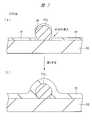
- (A) is sectional drawing which shows a mode that a thin protective film is formed on the glass substrate to which the foreign material adhered by CVD method
- (b) is thick protection on the glass substrate to which the foreign material adhered by CVD method.
- FIG. 18 is a schematic view showing a cross-sectional configuration of the mask holder, and is a cross-sectional view taken along line AA of FIG. It is a figure explaining the operation
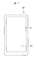
- FIG. 1 is a plan view of a mobile phone (smartphone) MP viewed from the front side.
- the mobile phone MP in the present embodiment has a substantially rectangular shape, and a display unit DU for displaying an image is provided on the front side of the mobile phone MP.
- the display unit DU in the present embodiment is an organic EL display unit (organic electroluminescence display unit) using an organic EL element.
- the mobile phone MP also includes a circuit unit that drives the display unit DU.
- the display unit DU a plurality of pixels are arranged in an array, and an image can be displayed.
- Various circuits are formed in the circuit section as necessary.
- the circuit unit is configured to include a drive circuit that is electrically connected to each of a plurality of pixels that form the display unit DU, and the drive circuit includes a plurality of pixels that form the display unit DU.
- the display unit DU is configured to display an image.
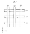
- FIG. 2 is a plan view schematically showing a layout configuration formed in a region RA which is a partial region of the display unit DU.
- the region RA for example, the lower electrode layers ELB extending in the x direction are arranged side by side while being spaced apart from each other in the y direction, and the upper electrode layers extending in the y direction, respectively.
- the ELAs are arranged side by side while being spaced apart in the x direction. Therefore, in the region RA, the lower electrode layer ELB and the upper electrode layer ELA are laid out so as to intersect each other.
- FIG. 3 is a cross-sectional view taken along line AA of FIG.
- a passivation film PAS is formed on a glass substrate GS that is transparent to visible light.
- the passivation film PAS is made of an insulating material (insulating film), for example, a silicon oxide film.
- the passivation film PAS may not be formed on the glass substrate GS, but it is more preferable to form it.
- the passivation film PAS can be formed over almost the entire top surface of the glass substrate GS.
- the passivation film PAS has a function of preventing moisture from entering the organic EL element (particularly, the organic layer OEL) from the glass substrate GS side. For this reason, the passivation film PAS functions as a protective film below the organic EL element.
- the protective film PF functions as a protective film on the upper side of the organic EL element, and has a function of preventing moisture from entering the organic EL element (particularly, the organic layer OEL) from the upper side. .
- An organic EL element is formed on the upper surface of the glass substrate GS via a passivation film PAS.
- the organic EL element includes a lower electrode layer ELB, an organic layer OEL, and an upper electrode layer ELA. That is, on the passivation film PAS on the glass substrate GS, the lower electrode layer ELB, the organic layer OEL, and the upper electrode layer ELA are sequentially stacked from the bottom, and the lower electrode layer ELB and the organic layer are stacked.
- the OEL and the upper electrode layer ELA constitute an organic EL element.
- the lower electrode layer ELB constitutes one of an anode and a cathode
- the upper electrode layer ELA constitutes the other of the anode and the cathode. That is, when the lower electrode layer ELB is an anode (anode layer), the upper electrode layer ELA is a cathode (cathode layer), and when the lower electrode layer ELB is a cathode (cathode layer), the upper electrode layer ELA is an anode (cathode layer). Anode layer).
- the lower electrode layer ELB and the upper electrode layer ELA are each made of a conductive film.
- One of the lower electrode layer ELB and the upper electrode layer ELA is desirably composed of a metal film such as an aluminum film (Al film) so that it can function as a reflective electrode.
- the other of the lower electrode layer ELB and the upper electrode layer ELA is preferably composed of a transparent conductor film made of ITO (indium tin oxide) or the like so that it can function as a transparent electrode.
- the lower electrode layer ELB can be a transparent electrode.
- the upper electrode layer ELA can be a transparent electrode.
- the glass substrate GS can be a transparent substrate having a light-transmitting property with respect to visible light.
- the organic layer OEL is formed on the lower electrode layer ELB, and the upper electrode layer ELA is formed on the organic layer OEL.
- the organic layer OEL is interposed between the lower electrode layer ELB and the upper electrode layer ELA.
- the organic layer OEL includes at least an organic light emitting layer.
- the organic layer OEL can further include an arbitrary layer among a hole transport layer, a hole injection layer, an electron transport layer, and an electron injection layer, if necessary, in addition to the organic light emitting layer. Therefore, the organic layer OEL includes, for example, a single layer structure of an organic light emitting layer, a stacked structure of a hole transport layer, an organic light emitting layer, and an electron transport layer, a hole injection layer, a hole transport layer, an organic light emitting layer, and an electron transport. A layered structure of a layer and an electron injection layer is formed.
- the lower electrode layer ELB constitutes a striped pattern extending in the x direction, for example. That is, each of the lower electrode layers ELB extends in the x direction and is arrayed at a predetermined interval in the y direction.
- the upper electrode layer ELA forms, for example, a stripe pattern extending in the y direction. That is, a plurality of upper electrode layers ELA are arranged at predetermined intervals in the x direction while extending in the y direction. That is, the lower electrode layer ELB is composed of a striped electrode group extending in the x direction, and the upper electrode layer ELA is composed of a striped electrode group extending in the y direction.
- the x direction and the y direction are directions that intersect each other, and more specifically, are directions that are orthogonal to each other. Further, the x direction and the y direction are also directions substantially parallel to the upper surface of the glass substrate GS.
- plan view refers to the case of viewing in a plane substantially parallel to the upper surface of the glass substrate GS.
- the organic layer OEL is sandwiched between the lower electrode layer ELB and the upper electrode ELA. Accordingly, an organic EL element composed of the lower electrode ELB, the upper electrode ELA, and the organic layer OEL is formed at each intersection of the lower electrode layer ELB and the upper electrode ELA, and a pixel is formed by the organic EL element. Is done.
- the organic light emitting layer in the organic layer OEL sandwiched between the lower electrode ELB and the upper electrode ELA emits light.
- the organic layer OEL can be formed over the entire display unit DU, but can also be formed in the same pattern as the lower electrode layer ELB. Similarly, the organic layer OEL can be formed in the same pattern as the upper electrode layer ELA. In any case, the organic layer OEL exists at each intersection of the lower electrode layer ELB and the upper electrode layer ELA.
- the organic EL elements constituting the pixels are arranged in an array on the glass substrate GS in the plan view in the display unit DU.
- the lower electrode layer ELB and the upper electrode layer ELA are formed of a stripe pattern.
- the organic EL elements arranged in the x direction have a common lower electrode layer ELB.
- the organic EL elements arranged in the y direction have a common upper electrode layer ELA.
- the present invention is not limited to this, and the structure of the organic EL elements arranged in an array can be variously changed.
- each organic EL element arranged in an array may not be connected to each other in either the upper electrode layer ELA or the lower electrode layer ELB, and may be arranged independently.
- each organic EL element is formed from an isolated pattern having a laminated structure of a lower electrode layer, an organic layer, and an upper electrode layer, and a plurality of these isolated organic EL elements are arranged in an array.
- an active element such as a TFT (thin film transistor) can be provided in addition to the organic EL element, and the pixels can be connected to each other by wiring.
- a protective film PF is formed on the upper surface of the glass substrate GS (passivation film PAS) so as to cover the organic EL element, and thus cover the lower electrode layer ELB, the organic layer OEL, and the upper electrode layer ELA. .
- the protective film PF is formed so as to cover the organic EL elements arranged in the array. For this reason, it is desirable that the protective film PF be formed on the entire display unit DU. Moreover, it is desirable to form over substantially the whole upper surface of the glass substrate GS.
- a resin film PIF is formed on the protective film PF.
- the material of the resin film PIF is made of, for example, PET (polyethylene terephthalate).
- the formation of the resin film PIF can be omitted.
- the case where the resin film PIF is formed is more preferable than the case where the resin film PIF is not formed. Since the resin film PIF is soft, the display unit DU can be easily handled by providing the resin film PIF. As described above, the display unit DU of the mobile phone MP is configured.
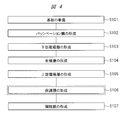
- FIG. 4 is a flowchart showing the flow of the manufacturing process of the display unit DU.
- a glass substrate having transparency to visible light is prepared (S101).
- a passivation film is formed on the upper surface of the glass substrate (S102).
- the passivation film can be formed using, for example, a sputtering method, a CVD (Chemical Vapor Deposition) method, or an ALD (Atomic Layer Deposition) method.
- the passivation film is made of an insulating material, for example, a silicon oxide film.
- a silicon oxide film formed by a CVD method can be used as a passivation film.
- an organic EL element including a lower electrode layer, an organic layer on the lower electrode layer, and an upper electrode layer on the organic layer is formed on the passivation film. That is, a lower electrode layer, an organic layer, and an upper electrode layer are sequentially formed on the passivation film (S103 to S105). This step can be performed, for example, as follows.
- a lower electrode layer is formed on the passivation film (S103).
- the lower electrode layer can be formed, for example, by forming a conductive film on the passivation film and then patterning the conductor film using a photolithography technique and an etching technique. Thereafter, an organic layer is formed on the lower electrode layer (S104).
- the organic layer can be formed by, for example, an evaporation method using a mask (vacuum evaporation method).
- an upper electrode layer is formed on the organic layer (S105).
- the upper electrode layer can be formed by, for example, a vapor deposition method using a mask.
- a protective film is formed on the upper electrode (S106).
- the protective film is formed so as to cover the organic EL element.
- the plurality of organic EL elements are arranged in an array, the plurality of organic EL elements are covered with a protective film.
- the protective film is formed of, for example, any one of a silicon oxide film, a silicon nitride film, a silicon oxynitride film, an aluminum oxide film, and an aluminum oxynitride film.
- the resin film is made of PET, for example, and can be formed by using a spin coating method (coating method).
- the display unit DU can be manufactured as described above.
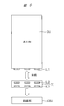
- FIG. 5 is a diagram schematically illustrating a configuration example in which the display unit DU and the circuit unit CRU are electrically connected.
- an electrode EL1 electrically connected to a pixel (organic EL element) constituting the display unit DU is formed in a frame region surrounding the display unit DU, and the electrode formed in this frame region EL1 is electrically connected to a pixel (organic EL element) constituting the display unit DU.
- the electrode EL1 is connected to the electrode EL2 formed on the connection tape electrode TE.
- the electrode EL3 electrically connected to the electrode EL2 is formed on the connecting tape electrode TE together with the electrode EL2, and the electrode EL3 is electrically connected to the circuit unit CRU.
- the display unit DU has a circuit unit CRU in a path of the electrode EL1 formed in the frame region ⁇ the electrode EL2 formed on the connection tape electrode TE ⁇ the electrode EL3 formed on the connection tape electrode TE ⁇ the circuit unit CRU. And electrically connected.
- the electrode formed in the frame region is arranged by overlapping the electrode EL2 formed in the connection tape electrode TE on the electrode EL1 formed in the frame region surrounding the display unit DU.
- EL1 and electrode EL2 constituting connection tape electrode TE are electrically connected. Therefore, in order to ensure the electrical connection between the electrode EL1 and the electrode EL2, it is necessary to prevent the protective film from being formed so as to cover the electrode EL1. This is because if a protective film made of an insulating film is formed so as to cover the electrode EL1, the electrode EL1 and the electrode EL2 of the connecting tape electrode TE cannot be electrically connected.
- the protective film needs to be formed so as to cover the pixel (organic EL element) formed in the display unit DU in order to protect the organic EL element from intrusion of moisture, while being connected to the electrode EL1.
- the protective film In order to ensure conduction between the tape electrode TE and the electrode EL2, it is not necessary to form the tape electrode TE in the frame region where the electrode EL1 is formed.
- the protective film needs to be formed so as to cover the pixels (organic EL elements) formed in the display unit DU, but not to be formed in the frame region where the electrode EL1 is formed. is there.
- the protective film since one glass substrate GS has a plurality of regions for forming the display unit DU, for example, a glass substrate GS on which an organic EL element is formed without using a mask. If a protective film is formed on the entire main surface, the protective film is formed not only on the display unit DU but also on the frame region surrounding the display unit DU.
- a protective film is formed so as to cover the electrode EL1 formed in the frame region, thereby ensuring conduction between the electrode EL1 and the electrode EL2 of the connecting tape electrode TE. Will not be able to. Therefore, a mask is required when forming the protective film. That is, as shown in FIG. 6, the protective film is formed in a state where a mask MK having an opening region OPR corresponding to the display unit DU and a covering region CVR corresponding to the frame region is overlaid on the glass substrate GS.
- a protective film is formed on the region of the glass substrate GS exposed from the opening region OPR formed on the mask MK (region on which the display unit DU is formed), while being covered with the covering region CVR formed on the mask MK.
- the protective film is not formed in the region of the glass substrate GS (region serving as the frame region).
- a mask MK having an opening region OPR corresponding to the display unit DU and a covering region CVR corresponding to the frame region is used. Accordingly, a protective film can be formed so as to cover the pixels (organic EL elements) formed in the display unit DU, and the protective film is not formed in the frame region where the electrode EL1 is formed. be able to.
- the protective film for protecting the organic EL element from the ingress of moisture is formed by using, for example, an atomic layer growth method (ALD method). The reason for this will be described below.
- the atomic layer growth method is a film forming method for forming a film in units of atomic layers on a substrate by alternately supplying a source gas and a reaction gas onto the substrate.
- This atomic layer growth method has an advantage that it is excellent in step coverage and film thickness controllability because a film is formed in units of atomic layers.
- the protective film that can fully function to protect the organic EL element from the ingress of moisture while reducing the film thickness according to the atomic layer growth method. Can be formed.
- the atomic layer growth method is used to form a protective film that protects the organic EL element from the ingress of moisture.
- the protective film PF is formed on the glass substrate GS to which the foreign object PCL is attached.
- the CVD method it is conceivable to use the CVD method as a method for forming the protective film PF.
- the vertical directivity tends to be strong.
- the protective film PF is not formed.
- the protective film PF is formed so as to cover the glass substrate GS to which the foreign substance PCL adheres due to a tendency to have high vertical directivity, and the protective film is formed on the step portion between the foreign substance PCL and the glass substrate GS.
- a dead space in which no PF is formed is born, and moisture permeates into the organic EL element from this dead space. For this reason, when forming the protective film PF by the CVD method, for example, as shown in FIG.
- a protective film PF is formed so as to completely cover. That is, when the protective film PF is formed by the CVD method with strong vertical directivity, by increasing the film thickness of the protective film PF, there is a dead space where the protective film PF is not formed at the step portion between the foreign matter PCL and the glass substrate GS. It will suppress birth. That is, it is difficult to completely prevent the foreign matter PCL from adhering to the glass substrate GS. Therefore, in consideration of the foreign matter PCL from adhering to the glass substrate GS, the protective film PF is applied to the organic EL element. In order to effectively prevent moisture from entering, when the CVD method is used to form the protective film PF, it is necessary to increase the thickness of the protective film PF.
- a plasma atomic layer growth method is used as a method of forming the protective film PF.
- a source gas and a reactive gas are alternately supplied and a reactive gas is supplied between a lower electrode holding a substrate and an upper electrode disposed opposite to the lower electrode.
- a film is formed on the substrate in units of atomic layers by performing plasma discharge.
- a film having excellent step coverage can be formed by forming a film in units of atomic layers.
- the plasma atomic layer growth apparatus in order to improve the step coverage, a material that is easy to diffuse is used as the source gas, and each gas (source gas, purge gas, and reactive gas) is sufficiently contained in the film formation container. Each gas is alternately supplied while ensuring a sufficient time for diffusion. Therefore, in the plasma atomic layer growth apparatus, the film is formed by the reaction between the source gas and the reactive gas even in a minute gap. That is, in the atomic layer growth apparatus, (1) a film is formed in units of atomic layers, (2) the source gas and the reactive gas are distributed to every corner of the minute gap, and (3) a place where no plasma discharge occurs. However, as a result of the feature that the raw material gas and the reactive gas are easily reacted, a film is also formed in a minute gap.
- the protective film PF can be formed so as to cover the glass substrate GS to which the foreign matter PCL is attached. That is, since the plasma atomic layer growth method is excellent in the step coverage, it is possible to prevent the formation of a dead space in which the protective film PF is not formed at the stepped portion between the foreign matter PCL and the glass substrate GS. Although the film thickness is reduced, the intrusion of moisture into the organic EL element can be effectively suppressed. That is, when forming the protective film PF by the plasma atomic layer growth method, it is possible to form the protective film PF that can effectively suppress the intrusion of moisture into the organic EL element without increasing the film thickness. It is.
- the moisture content can be increased without increasing the film thickness even when the foreign substance PCL is attached to the glass substrate GS.
- the protective film PF excellent in the intrusion prevention effect. Therefore, it is desirable to form the protective film PF that effectively protects moisture from entering the organic EL element by using the plasma atomic layer growth method.
- the thickness of the protective film PF can be reduced.
- the plasma atomic layer growth method is configured to form the display unit DU on the flexible substrate. It is also effective to apply the protective film PF formed by the above.
- FIG. 9 is a diagram schematically showing a state where the flexible substrate 1S is used as the substrate of the display unit DU and the flexible substrate 1S is bent.
- a passivation film PAS is formed on the flexible substrate 1S
- an organic EL layer OLDL is formed on the passivation film PAS
- a protective film PF is formed on the organic EL layer OLDL.
- a bent state of the display unit DU in which the resin film PIF is formed on the film PF is illustrated.
- the display unit DU can be bent by forming the display unit DU on the flexible substrate 1S.
- the flexible substrate 1S When the flexible substrate 1S is used as the substrate, there is a risk that cracks may occur in the protective film PF made of an inorganic insulating film with bending. For this reason, it is desirable to make the protective film PF made of an inorganic insulating film as thin as possible.
- the thickness of the protective film PF can be reduced by employing the protective film PF formed using the plasma atomic layer growth method. As a result, it is possible to efficiently obtain the effect of preventing the penetration of moisture by the protective film PF while suppressing the formation of cracks in the protective film PF made of an inorganic insulating film.
- the protective film PF formed by using the method is useful.
- FIG. 10 is a flowchart for explaining the flow of a method for forming a protective film by the plasma atomic layer growth method.
- the glass substrate is mounted on the lower electrode (stage) of the plasma atomic layer growth apparatus.
- a source gas is introduced from the gas supply unit of the plasma atomic layer growth apparatus into the film formation container (processing chamber) (S201).
- the source gas is supplied into the film formation container for 0.1 seconds, for example.
- the source gas is supplied into the film formation container, and the source gas is adsorbed on the glass substrate to form an adsorption layer.
- a purge gas is introduced from the gas supply unit into the film formation container (processing chamber) (S202).
- the purge gas is supplied into the film forming container, while the source gas is discharged from the exhaust unit to the outside of the film forming container.
- the purge gas is supplied into the film formation container for 0.1 seconds, for example.
- the exhaust unit exhausts the source gas and the purge gas in the film formation container for 2 seconds, for example. Thereby, the purge gas is supplied into the film forming container, and the source gas not adsorbed on the glass substrate is purged from the film forming container.
- a reactive gas is supplied from the gas supply unit (S203). Thereby, the reactive gas is supplied into the film forming container.
- the reaction gas is supplied into the film formation container for 1 second, for example.
- plasma discharge is generated by applying a discharge voltage between the upper electrode and the lower electrode (S204). As a result, radicals (active species) are generated in the reaction gas.
- a reaction is supplied into the film formation container, and the adsorption layer adsorbed on the glass substrate chemically reacts with the reaction gas, whereby a protective film made of an atomic layer is formed.
- the purge gas is supplied from the gas supply unit (S205).
- the purge gas is supplied into the film forming container, while the reaction gas is discharged from the exhaust unit to the outside of the film forming container.
- the purge gas is supplied into the film formation container for 0.1 seconds, for example.
- an exhaust part exhausts the reaction gas and purge gas in a film-forming container for 2 seconds, for example.
- purge gas is supplied into the film formation container, and excess reaction gas that is not used for the reaction is purged from the film formation container.
- a protective film composed of a single atomic layer is formed on the glass substrate. Thereafter, the above-described steps (S201 to S205) are repeated a predetermined number of times (S206), thereby forming a protective film composed of a plurality of atomic layers. Thereby, the film forming process is completed (S207).
- the protective film PF can be formed by the plasma atomic layer growth method.
- the protective film for protecting the organic EL element from moisture intrusion is formed by a plasma atomic layer growth method using a mask having an opening region corresponding to the display portion and a covering region corresponding to the frame region. Can do.
- mask MK is necessary when forming the protective film, and this mask MK is, for example, a glass substrate. It is about the same size as GS. This is because it is necessary to form a protective film at once for all the regions of the glass substrate GS corresponding to the plurality of display units DU, and when forming the protective film, the protective film is formed on all the frame regions. This is because it is necessary to cover all the regions (regions other than the plurality of display units DU) that are the frame regions so that the image is not formed.
- the size of the glass substrate GS is increasing.
- the size of the mask MK having the same size as that of the glass substrate GS is also increased.
- the increase in the size of the mask MK creates a situation where it is difficult to ensure the flatness of the mask MK. This is because as the size of the mask MK increases, the weight of the mask MK itself increases. As a result, the mask MK is likely to bend, and it is difficult to ensure the flatness of the mask MK.
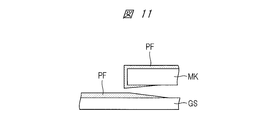
- FIG. 11 is a diagram schematically illustrating a state in which the protective film is formed so as to enter a minute gap generated between the glass substrate GS and the mask MK.
- an electrode that is electrically connected to the display portion is formed in the frame region that exists below the mask MK. If a protective film made of an insulating material is formed on the electrode, It becomes impossible to ensure conduction between the display unit and the circuit unit.
- each gas source gas, purge gas, and reactive gas
- Each gas is alternately supplied while ensuring a sufficient time to diffuse into the membrane container. For this reason, for example, the source gas and the reaction gas are distributed not only on the substrate but also every corner of the film formation container.
- active species radiations are formed by plasma discharge of the reactive gas, and the active species and the source gas adsorbed on the substrate react to form a film.
- a film is formed by the reaction between the source gas and the reactive gas even in a minute gap where no plasma discharge occurs.
- a film is formed in units of atomic layers, (2) a source gas or a reactive gas is distributed to every corner of the film formation container, and (3) a place where no plasma discharge occurs.
- a film is also formed in a minute gap generated between the mask MK and the glass substrate GS, for example.
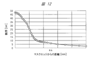
- FIG. 12 is a graph showing the relationship between the distance entering the mask side from the mask edge and the thickness of the protective film formed in the related art.
- the horizontal axis indicates the distance (mm) entering the mask side from the mask edge
- the vertical axis indicates the film thickness (nm) of the protective film to be formed.
- the protective film is also formed at the position where the mask edge enters the mask side. That is, it can be seen from the actual measurement results shown in FIG. 11 that in the related technique, a protective film is also formed on a part of the frame region of the glass substrate GS that should be covered with the mask.
- a mobile phone smart phone
- the protection film is likely to be formed so as to cover the electrode formed in the frame region by entering the protection film.
- the electrical connection between the display unit and the circuit unit through the electrode cannot be ensured.
- the size of the frame area is increased and the electrodes are formed in the inner area where the protective film does not enter, the size of the display area is increased due to the increased size of the frame area. Nevertheless, the overall size of the mobile phone becomes large. Therefore, in the related art, there is room for improvement from the viewpoint of securing the electrical connection reliability between the display unit and the circuit unit through the electrodes formed in the frame region while reducing the size of the frame region. You can see that it exists.
- the main reason for the penetration of the protective film into the frame region is that a fine gap is generated between the glass substrate and the mask, it is conceivable to eliminate this fine gap.
- this fine gap is caused by a decrease in the flatness of the mask, it can be considered to cope with the selection of a mask material constituting the mask.
- the mask material is made of metal
- the distance to which the protective film enters is about 3 mm
- the distance to which the protective film enters is about 1 mm. From this, it is considered that the protective film can be prevented from entering the frame region by changing the mask material from metal to ceramic.
- the measure of changing the material of the mask is not an essential measure, and a further fundamental measure is required.
- the mask MK having high rigidity if a completely flat mask MK cannot be manufactured, for example, a fine gap is generated between the mask MK and the glass substrate GS as shown in FIG. In other words, if the mask MK with high rigidity cannot achieve perfect flatness, a fine gap is generated between the mask MK and the glass substrate GS because the rigidity is rather high.
- the method of manufacturing the mask MK having a high rigidity by increasing the thickness of the mask MK is actually a mask MK. It is considered difficult to ensure the flatness of the film.
- the thickness of the mask MK is reduced, the rigidity of the mask MK is reduced.
- the mask MK is reflected on the glass substrate GS having an uneven shape, reflecting the uneven shape of the glass substrate GS. Can be arranged. That is, as a result of the low rigidity of the mask MK having a small thickness, the mask MK becomes familiar with the glass substrate GS having an uneven shape, and the adhesion between the mask MK and the glass substrate GS can be improved.
- a thin mask MK with low rigidity is more desirable.
- the thin mask MK is difficult to hold with the pin PN as a result of low rigidity.
- the thin mask MK is useful from the viewpoint of improving the adhesion between the mask MK and the glass substrate GS, but needs to be devised from the viewpoint of holding the thin mask MK.
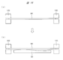
- the method of applying tension to the thin mask MK and fixing both ends of the mask MK with the holding member 100 is effective from the viewpoint of holding the mask MK, but the thin mask MK that follows the uneven shape of the glass substrate GS.
- the sacrifice of losing the benefits of. Therefore, the method of applying tension to the thin mask MK and fixing both ends of the mask MK with the holding member 100 ensures that the thin mask MK is secured while maintaining the advantage of the thin mask MK that conforms to the uneven shape of the glass substrate GS. It is difficult to achieve this. That is, in order to achieve both the improvement of the adhesion between the mask MK and the glass substrate GS and the reliable holding of the mask MK, a device is required.
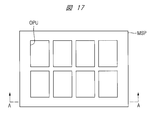
- FIG. 17 is a plan view showing a planar configuration of the mask holder MSP in the present embodiment.
- the mask holder MSP in the present embodiment has a rectangular planar shape, and a plurality of openings OPU are formed therein.
- the mask holder MSP is configured to be disposed on the mask MK shown in FIG. 6, and in particular, the opening portion OPU of the mask holder MSP is positioned on the opening region OPR of the mask MK shown in FIG. It is comprised so that it may be arranged.
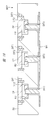
- FIG. 18 is a schematic diagram showing a cross-sectional configuration of the mask holder MSP, which is a cross-sectional view taken along the line AA in FIG.
- the mask holder MSP in the present embodiment is configured to hold the mask MK, and can suspend the mask MK and can be moved up and down.
- a support part SU that can support the suspension part HU and can be separated from the suspension part HU.
- the support unit SU has a front surface (upper surface) and a back surface (lower surface) opposite to the front surface. As shown in FIG. 18, the support unit SU has a groove formed on the surface. DIT1, a groove DIT2 communicating with the groove DIT1, and having a width smaller than the width of the groove DIT1, and formed on the back surface, communicating with the groove DIT2, and having a width smaller than the width of the groove DIT2. A groove DIT3 is formed.
- the suspension part HU is arranged inside the groove DIT2 and can move in the vertical direction, and is configured to be able to contact / non-contact the bottom surface of the groove DIT2.
- the back surface of the support unit SU is configured to be able to contact / non-contact with the mask MK.
- the support unit SU is provided with a cap CP for embedding the groove DIT1.
- the suspension part HU is configured to be movable in the thickness direction (vertical direction) of the support part SU. When the mask MK suspended from the suspension part HU contacts the back surface of the support part SU, the suspension part HU is suspended. A gap is formed between the upper surface of the part HU and the lower surface of the cap CP.
- the mask MK is welded to a plurality of shafts, and threading is formed at the tip of the shaft. And each tip part of a plurality of shafts is inserted in a screw hole formed in each of a plurality of suspension parts HU, and thereby, each of a plurality of shafts, each of a plurality of suspension parts HU, and Is connected. As a result, the mask MK is suspended from the suspension part HU via the shaft.
- the suspension part HU is configured to be able to suspend the mask MK.
- a cap CP is embedded in the groove DIT1 that communicates with the groove DIT2 in which the suspension part HU is disposed, and the cap CP is fixed to the support part SU by screws, for example.
- the suspending portion HU there is a gap between the suspending portion HU and the cap CP, and the suspending portion HU is formed in a size that does not contact the cap CP even when the suspending portion HU moves in the vertical direction. That is, the mask holding body MSP in the present embodiment has a suspended portion even when the mask MK suspended by the suspended portion HU comes into contact with the support portion SU due to the upward movement of the suspended portion HU.
- the gap is formed between the HU and the cap CP.
- the thickness of the support portion SU is much thicker than the thickness of the suspension portion HU, and the mass of the support portion SU is larger than the mass of the suspension portion HU. It has become.
- the mask MK is thin so as to have low rigidity. For example, the thickness of the mask MK is smaller than 1 mm.
- the mask holder MSP in the present embodiment is configured as described above, and the operation for placing the mask MK on the substrate using the mask holder MSP in the present embodiment will be described below. The description will be given with reference.
- a step of placing a mask MK on a glass substrate mounted on the substrate mounting portion a step of placing a mask MK on a glass substrate mounted on the substrate mounting portion.
- an operation of placing the mask MK on the glass substrate by the mask holder MSP will be described.
- the step of placing the substrate on the substrate mounting portion, the step of placing the mask MK on the glass substrate by the mask holder MSP, the step of supplying the source gas above the glass substrate, and the upper side of the glass substrate In the film forming method including the step of supplying the reactive gas to the substrate and the step of generating plasma above the glass substrate, the operation of placing the mask MK on the glass substrate by the mask holder MSP will be described.
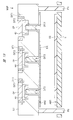
- the mask holder MSP is supported by pins PN so as to be positioned above the glass substrate GS disposed on the stage (substrate mounting part) ST.
- the mask holder MSP has a suspension part HU that suspends the mask MK and a support part SU that supports the suspension part HU, and the mask MK is suspended by the suspension part HU disposed inside the support part SU. It has been. That is, the mask MK is suspended by the suspension part HU in a state where the suspension part HU is supported by the support part SU by bringing the suspension part HU into contact with the bottom surface of the groove DIT2 formed in the support part SU.
- the mask MK is separated from the back surface of the support part SU, and a tensile force from the suspension part HU is applied to the mask MK.
- the thickness of this mask MK is smaller than the thickness of the glass substrate GS. Note that an alignment mark AM1 is formed on the glass substrate GS, and an alignment mark AM2 is formed on the mask MK.
- the stage ST on which the glass substrate GS is mounted is moved upward. Thereby, the distance between the glass substrate GS and the mask MK suspended by the mask holder MSP is reduced. As described above, the alignment between the glass substrate GS and the mask MK is performed in a state where the distance between the glass substrate GS and the mask MK suspended by the mask holder MSP is reduced. Specifically, the stage ST on which the glass substrate GS is mounted is moved in the horizontal direction so that the alignment mark AM1 formed on the glass substrate GS and the alignment mark AM2 formed on the mask MK coincide in a plane. Move in the (left-right direction).
- the pin PN supporting the mask holding body MSP is moved downward, so that the glass substrate GS and the mask holding body MSP The distance from the suspended mask MK may be reduced.
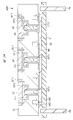
- the stage ST is further raised to bring the glass substrate GS and the mask MK into contact. That is, after positioning the glass substrate GS and the mask MK, the mask MK suspended by the suspension part HU is brought into contact with the glass substrate GS while the suspension part HU is supported by the support part SU. At this time, since the mask MK is supported by the glass substrate GS, the tensile force from the suspension part HU is not applied to the mask MK.
- the mask MK is deformed so as to follow the uneven shape on the surface of the glass substrate GS. In other words, since the mask MK is low in rigidity, the mask MK is arranged so as to conform to the surface of the glass substrate GS.
- the glass substrate GS and the mask MK are moved by moving the pin PN supporting the mask holder MSP downward. You may make it contact.
- the stage ST on which the glass substrate GS is mounted is raised.
- the suspension part HU is separated from the support part SU while maintaining the state in which the mask MK is in contact with the glass substrate GS.
- gravity based on the mass of the suspension part HU (including the shaft) is applied to the mask MK, a pressing force from the suspension part HU is applied to the mask MK. Therefore, this pressing force further improves the adhesion between the glass substrate GS and the mask MK.
- the pin PN supporting the mask holder MSP is moved downward to bring the mask MK into contact with the glass substrate GS. While maintaining, the suspension part HU may be separated from the support part SU.
- the mask MK is brought into contact with the back surface of the mask holder MSP.
- the mask MK may be brought into contact with the back surface of the mask holder MSP by moving the pin PN supporting the mask holder MSP downward.
- the pin PN supporting the mask holder MSP is lowered. Accordingly, the support unit SU is brought into contact with the mask MK while maintaining the state where the suspension unit HU is separated from the support unit SU. As a result, gravity based on the mass of the support part SU is applied to the mask MK. That is, in this state, a pressing force is applied to the mask MK from the suspension portion HU, and a pressing force from the support portion SU is further applied to the mask MK. Therefore, the adhesion between the glass substrate GS and the mask MK is further improved by adding the pressing force from the suspension part HU and the pressing force from the support part SU. In particular, since the mass of the support part SU is much larger than the mass of the suspension part HU, the effect of improving the adhesion between the glass substrate GS and the mask MK is increased by applying a pressing force from the support part SU.
- the operation of arranging the mask MK on the glass substrate GS using the mask holder MSP is completed. Thereafter, while maintaining the state in which the mask MK is disposed on the glass substrate GS and the mask holder MSP is disposed on the mask MK, the film is formed on the glass substrate GS by the plasma atomic layer growth apparatus. Processing is performed.
- the first feature point in the present embodiment is that the mask MK is held by the suspension part HU in a state where the suspension part HU of the mask holder MSP is supported by the support part SU of the mask holder MSP.
- the point is that the mask MK suspended by the suspension part HU is brought into contact with the glass substrate GS while being suspended.
- the suspension portion is used while following the uneven shape of the glass substrate GS and using the thin and low-rigidity mask MK having the advantage of improving the adhesion with the glass substrate GS.
- the thin and low-rigidity mask MK that is difficult to support with pins can be reliably supported. That is, in the present embodiment, by using the mask holder MSP having the suspension part HU that suspends the mask MK and the support part SU that supports the suspension part HU, the thin and low-rigidity mask MK is supported. It is possible to improve both the adhesion between the glass substrate GS and the mask MK and the ease of holding the mask MK. As a result, according to the present embodiment, it is possible to improve the adhesion between the glass substrate GS and the mask MK and suppress the generation of a fine gap between the glass substrate GS and the mask MK.
- the film on the region of the glass substrate GS covered with the mask MK is used.
- the formation of can be suppressed. Therefore, according to the present embodiment, the protective film is formed on the glass substrate GS using the mask MK having the opening region OPR corresponding to the display unit DU shown in FIG. 6 and the covering region CVR corresponding to the frame region.
- a protective film can be formed so as to cover the pixel (organic EL element) formed in the display portion DU, and the protective film is not formed in the frame region where the electrode is formed. be able to.
- the connection reliability between the electrode EL1 electrically connected to the display unit DU shown in FIG. 5 and the electrode EL2 formed on the connection tape electrode TE is improved. can do.
- the reliability of the electronic device including the display unit DU can be improved from the viewpoint of focusing on the electronic device that is the final product, and from the viewpoint of focusing on the manufacturing process of the electronic device, This means that the production yield of the electronic device including the display unit DU can be improved. Therefore, according to the first feature point in the present embodiment, a highly reliable electronic device can be realized while reducing the manufacturing cost of the electronic device.
- the second feature point in the present embodiment is that, for example, as shown in FIG. 24, the support part SU of the mask holder MSP is finally brought into contact with the mask MK. Thereby, the pressing force which presses against the glass substrate GS with respect to the mask MK from the support part SU of the mask holding body MSP can be applied. This means that it is possible to further improve the adhesion between the mask MK having low rigidity and the glass substrate GS, thereby further generating fine gaps between the mask MK and the glass substrate GS. Can be reduced.
- the mass of the support part SU is larger than the mass of the suspension part HU, it is possible to increase the pressing force applied to the mask MK, thereby generating a fine gap between the glass substrate GS and the mask MK. This can be effectively suppressed.
- the mask MK is also effective to configure the mask MK from a magnetic material from the viewpoint of effectively suppressing the generation of a fine gap between the glass substrate GS and the mask MK.
- the pressing force of the mask MK against the glass substrate GS can be further increased by embedding an electromagnet in the stage ST and attracting the mask MK made of a magnetic material to the electromagnet.
- the magnetic force from the electromagnet also acts on the mask holding body MSP, so that not only the pressing force based on the mass of the mask holding body MSP but also the pressing force based on the magnetic force is applied from the mask holding body MSP to the mask MK. Because it will join.
Landscapes
- Chemical & Material Sciences (AREA)
- Engineering & Computer Science (AREA)
- Metallurgy (AREA)
- General Chemical & Material Sciences (AREA)
- Chemical Kinetics & Catalysis (AREA)
- Materials Engineering (AREA)
- Mechanical Engineering (AREA)
- Organic Chemistry (AREA)
- Manufacturing & Machinery (AREA)
- Physics & Mathematics (AREA)
- Plasma & Fusion (AREA)
- Electromagnetism (AREA)
- Optics & Photonics (AREA)
- Electroluminescent Light Sources (AREA)
- Chemical Vapour Deposition (AREA)
Abstract
マスクと基板との隙間に膜が形成されてしまうことを抑制するために、マスクと基板との密着性を向上する技術を提供する。成膜方法は、吊り部HUを支持部SUで支持した状態で、吊り部HUによってマスクMKを吊る工程と、吊り部HUを支持部SUで支持した状態で、吊り部HUによって吊られたマスクMKをガラス基板GS上に接触させる工程とを有する。
Description
本発明は、成膜技術および電子装置の製造技術並びにマスク保持体に関し、例えば、有機EL(Electro-Luminescence)膜を保護する保護膜を形成する技術に適用して有効な技術に関する。
特開2005-339861号公報(特許文献1)には、メタルマスクに引張り力を付与した状態で支持フレームに固定されるマスク構造体に関する技術が記載されている。
特開2013-187019号公報(特許文献2)には、有機EL素子の表面を覆う保護膜に関する技術が記載されている。
例えば、マスクと基板との隙間に膜が形成されてしまうことを抑制するために、マスクと基板との密着性を向上する技術が望まれている。
その他の課題と新規な特徴は、本明細書の記述および添付図面から明らかになるであろう。
一実施の形態における成膜方法は、吊り部を支持部で支持した状態で、吊り部によってマスクを吊る工程と、吊り部を支持部で支持した状態で、吊り部によって吊られたマスクを基板上に接触させる工程とを有する。
一実施の形態における成膜技術によれば、成膜特性の向上を図ることができる。
実施の形態を説明するための全図において、同一の部材には原則として同一の符号を付し、その繰り返しの説明は省略する。なお、図面をわかりやすくするために平面図であってもハッチングを付す場合がある。
<携帯電話機の表示部の構成>
図1は、携帯電話機(スマートフォン)MPを表面側から見た平面図である。図1に示すように、本実施の形態における携帯電話機MPは、略矩形形状をしており、携帯電話機MPの表面側には、画像を表示するための表示部DUが設けられている。例えば、本実施の形態における表示部DUは、有機EL素子を利用した有機EL表示部(有機エレクトロルミネッセンス表示部)である。また、図示はしないが、携帯電話機MPは、表示部DUを駆動する回路部も有している。
図1は、携帯電話機(スマートフォン)MPを表面側から見た平面図である。図1に示すように、本実施の形態における携帯電話機MPは、略矩形形状をしており、携帯電話機MPの表面側には、画像を表示するための表示部DUが設けられている。例えば、本実施の形態における表示部DUは、有機EL素子を利用した有機EL表示部(有機エレクトロルミネッセンス表示部)である。また、図示はしないが、携帯電話機MPは、表示部DUを駆動する回路部も有している。
表示部DUには、複数の画素がアレイ状に配列されており、画像の表示を可能としている。回路部には、必要に応じて種々の回路が形成されている。例えば、回路部は、表示部DUを構成する複数の画素のそれぞれと電気的に接続された駆動回路を含むように構成されており、この駆動回路は、表示部DUを構成する複数の画素を制御することにより、表示部DUにおいて、画像を表示できるように構成されている。
次に、図2は、表示部DUの一部領域である領域RAに形成されているレイアウト構成を模式的に示す平面図である。図2に示すように、領域RAにおいては、例えば、それぞれx方向に延在する下部電極層ELBがy方向に離間しながら並んで配置されているとともに、それぞれy方向に延在する上部電極層ELAがx方向に離間しながら並んで配置されている。したがって、領域RAにおいては、下部電極層ELBと、上部電極層ELAとが交差するようにレイアウト配置されていることになる。
続いて、図3は、図2のA-A線で切断した断面図である。図3に示すように、例えば、可視光に対して透光性を有するガラス基板GS上には、パッシベーション膜PASが形成されている。パッシベーション膜PASは、絶縁材料(絶縁膜)からなり、例えば、酸化シリコン膜からなる。パッシベーション膜PASは、ガラス基板GS上に形成しない場合もあり得るが、形成した方がより望ましい。パッシベーション膜PASは、ガラス基板GSの上面のほぼ全体にわたって形成することができる。
パッシベーション膜PASは、ガラス基板GS側から有機EL素子(特に有機層OEL)への水分の浸入を防止する機能を有している。このため、パッシベーション膜PASは、有機EL素子の下側の保護膜として機能することになる。一方、保護膜PFは、有機EL素子の上側の保護膜として機能することになり、上側から有機EL素子(特に有機層OEL)への水分の浸入を防止する機能を有していることになる。
ガラス基板GSの上面上には、パッシベーション膜PASを介して、有機EL素子が形成されている。有機EL素子は、下部電極層ELBと有機層OELと上部電極層ELAとからなる。つまり、ガラス基板GS上のパッシベーション膜PAS上には、下部電極層ELBと有機層OELと上部電極層ELAとが、下から順に積層して形成されており、これらの下部電極層ELBと有機層OELと上部電極層ELAとにより、有機EL素子が構成されることになる。
下部電極層ELBは、陽極および陰極うちの一方を構成し、上部電極層ELAは、陽極および陰極うちの他方を構成する。すなわち、下部電極層ELBが陽極(陽極層)の場合は、上部電極層ELAは陰極(陰極層)であり、下部電極層ELBが陰極(陰極層)の場合は、上部電極層ELAは陽極(陽極層)である。下部電極層ELBおよび上部電極層ELAは、それぞれ導電膜からなる。
下部電極層ELBおよび上部電極層ELAのうちの一方は、反射電極として機能できるように、アルミニウム膜(Al膜)などの金属膜から構成することが望ましい。また、下部電極層ELBおよび上部電極層ELAのうちの他方は、透明電極として機能できるように、ITO(インジウムスズオキサイド)などからなる透明導体膜から構成することが望ましい。ガラス基板GSの下面側から光を取出す、いわゆるボトムエミッション方式を採用する場合は、下部電極層ELBを透明電極とすることができる。一方、ガラス基板GSの上面側から光を取出す、いわゆるトップエミッション方式を採用する場合は、上部電極層ELAを透明電極とすることができる。また、ボトムエミッション方式を採用する場合は、ガラス基板GSとして、可視光に対して透光性を有する透明基板とすることができる。
ガラス基板GS上のパッシベーション膜PAS上に下部電極層ELBが形成され、かつ、下部電極層ELB上に有機層OELが形成され、かつ、有機層OEL上に上部電極層ELAが形成されているため、下部電極層ELBと上部電極層ELAとの間には、有機層OELが介在していることになる。
有機層OELは、少なくとも有機発光層を含んでいる。有機層OELは、有機発光層以外にも、ホール輸送層、ホール注入層、電子輸送層および電子注入層のうちの任意の層を、必要に応じて更に含むことができる。このため、有機層OELは、例えば、有機発光層の単層構造や、ホール輸送層と有機発光層と電子輸送層との積層構造や、ホール注入層とホール輸送層と有機発光層と電子輸送層と電子注入層との積層構造などから構成される。
例えば、図2に示すように、下部電極層ELBは、例えば、x方向に延在するストライプ状のパターンを構成している。すなわち、下部電極層ELBのそれぞれは、x方向に延在しながら、y方向に所定の間隔で複数配列されている。一方、上部電極層ELAは、例えば、y方向に延在するストライプ状のパターンを構成している。すなわち、上部電極層ELAは、y方向に延在しながら、x方向に所定の間隔で複数配列されている。つまり、下部電極層ELBは、x方向に延在するストライプ状の電極群からなり、上部電極層ELAは、y方向に延在するストライプ状の電極群からなる。ここで、x方向とy方向とは、互いに交差する方向であり、より特定的には、互いに直交する方向である。また、x方向とy方向は、ガラス基板GSの上面に略平行な方向でもある。
下部電極層ELBの延在方向はx方向であり、上部電極層ELAの延在方向はy方向であるため、下部電極層ELBと上部電極層ELAとは、平面視において互いに交差している。なお、「平面視」とは、ガラス基板GSの上面に略平行な平面で見た場合を言う。
下部電極層ELBと上部電極層ELAとの各交差部においては、下部電極層ELBと上部電極ELAとで有機層OELが上下に挟まれた構造をしている。このことから、下部電極層ELBと上部電極ELAとの各交差部に、下部電極ELBと上部電極ELAと有機層OELとで構成される有機EL素子が形成され、その有機EL素子により画素が形成される。下部電極ELBと上部電極ELAとの間に所定の電圧を印加することにより、下部電極ELBと上部電極ELAとの間に挟まれた有機層OEL中の有機発光層が発光する。
なお、有機層OELは、表示部DUの全体にわたって形成することもできるが、下部電極層ELBと同じパターンとして形成することもできる。同様に、有機層OELは、上部電極層ELAと同じパターンとして形成することもできる。いずれにしても、下部電極層ELBと上部電極層ELAとの各交点には、有機層OELが存在している。
このように、平面視において、表示部DUでは、平面視において、ガラス基板GS上に画素を構成する有機EL素子がアレイ状に配置されていることになる。
なお、ここでは、下部電極層ELBおよび上部電極層ELAがストライプ状のパターンから構成されている場合について説明している。このため、アレイ状に配列した複数の有機EL素子(画素)において、x方向に並んだ有機EL素子同士は、共通の下部電極層ELBを有する。一方、y方向に並んだ有機EL素子同士では、共通の上部電極層ELAを有する。しかしながら、これに限定されず、アレイ状に配列する有機EL素子の構造は、種々変更可能である。
例えば、アレイ状に配置された数の有機EL素子が、上部電極層ELAでも下部電極層ELBでも互いにつながっておらず、独立に配置されている場合もあり得る。この場合は、各有機EL素子は、下部電極層と有機層と上部電極層との積層構造を有する孤立パターンから形成され、この孤立した有機EL素子が、アレイ状に複数配置されることになる。この場合、各画素においては、有機EL素子に加えてTFT(薄膜トランジスタ)などのアクティブ素子を設けるとともに、画素同士を配線で接続することができる。
ガラス基板GS(パッシベーション膜PAS)の上面上には、有機EL素子を覆うように、したがって下部電極層ELBと有機層OELと上部電極層ELAとを覆うように、保護膜PFが形成されている。表示部DUに有機EL素子がアレイ状に配列している場合は、アレイ状に配列した有機EL素子を覆うように、保護膜PFが形成されている。このため、保護膜PFは、表示部DUの全体に形成されていることが望ましい。また、ガラス基板GSの上面のほぼ全体上にわたって形成されていることが望ましい。有機EL素子を保護膜PFで覆うことにより、有機EL素子への水分の浸入(特に、有機層OELへの水分の浸入)を保護膜によって防止することができる。
保護膜PF上には、樹脂膜PIFが形成されている。樹脂膜PIFの材料としては、例えばPET(polyethylene terephthalate:ポリエチレンテレフタレート)などから構成される。樹脂膜PIFは、その形成を省略することもできる。ただし、樹脂膜PIFを形成しない場合よりも、樹脂膜PIFを形成する場合の方が望ましい。樹脂膜PIFは、柔らかいため、樹脂膜PIFを設けることにより、表示部DUを扱いやすくなる。以上のようにして、携帯電話機MPの表示部DUが構成されていることになる。
<表示部の製造方法>
次に、表示部DUの製造方法について、図面を参照しながら説明する。図4は、表示部DUの製造工程の流れを示すフローチャートである。まず、例えば、可視光に対して透光性を有するガラス基板を準備する(S101)。続いて、ガラス基板の上面上に、パッシベーション膜を形成する(S102)。パッシベーション膜は、例えば、スパッタリング法やCVD(Chemical Vapor Deposition)法やALD(Atomic Layer Deposition)法を使用して形成することができる。パッシベーション膜は、絶縁材料からなり、例えば、酸化シリコン膜からなる。特に、CVD法により形成した酸化シリコン膜を、パッシベーション膜として使用することができる。
次に、表示部DUの製造方法について、図面を参照しながら説明する。図4は、表示部DUの製造工程の流れを示すフローチャートである。まず、例えば、可視光に対して透光性を有するガラス基板を準備する(S101)。続いて、ガラス基板の上面上に、パッシベーション膜を形成する(S102)。パッシベーション膜は、例えば、スパッタリング法やCVD(Chemical Vapor Deposition)法やALD(Atomic Layer Deposition)法を使用して形成することができる。パッシベーション膜は、絶縁材料からなり、例えば、酸化シリコン膜からなる。特に、CVD法により形成した酸化シリコン膜を、パッシベーション膜として使用することができる。
次に、パッシベーション膜上に、下部電極層と、下部電極層上の有機層と、有機層上の上部電極層とからなる有機EL素子を形成する。すなわち、パッシベーション膜上に、下部電極層と有機層と上部電極層とを順に形成する(S103~S105)。この工程は、例えば、次のようにして行うことができる。
すなわち、パッシベーション膜上に下部電極層を形成する(S103)。下部電極層は、例えば、導電膜をパッシベーション膜上に形成した後、フォトリソグラフィ技術およびエッチング技術を使用して導体膜をパターニングすることにより形成することができる。その後、下部電極層上に有機層を形成する(S104)。有機層は、例えば、マスクを用いた蒸着法(真空蒸着法)により形成することができる。そして、有機層上に上部電極層を形成する(S105)。上部電極層は、例えば、マスクを用いた蒸着法により形成できる。
続いて、下部電極層と有機層と上部電極層とからなる有機EL素子を形成した後、上部電極上に保護膜を形成する(S106)。保護膜は、有機EL素子を覆うように形成される。複数の有機EL素子がアレイ状に配列している場合は、これらの複数の有機EL素子が保護膜で覆われることになる。保護膜は、例えば、酸化シリコン膜、窒化シリコン膜、酸窒化シリコン膜、酸化アルミニウム膜あるいは、酸窒化アルミニウム膜のいずれかの膜から形成される。
その後、保護膜上に樹脂膜を形成する(S107)。樹脂膜は、例えばPETからなり、スピンコート法(塗布法)を使用することにより形成することができる。以上のようにして、表示部DUを製造することができる。
<表示部と回路部との接続構成>
表示部において画像を表示するためには、表示部を構成する複数の画素(有機EL素子)を駆動制御する必要があり、この有機EL素子を駆動制御する機能が回路部で実現される。したがって、表示部において画像を表示させるため、表示部は、回路部と電気的に接続される必要がある。
表示部において画像を表示するためには、表示部を構成する複数の画素(有機EL素子)を駆動制御する必要があり、この有機EL素子を駆動制御する機能が回路部で実現される。したがって、表示部において画像を表示させるため、表示部は、回路部と電気的に接続される必要がある。
図5は、表示部DUと回路部CRUとを電気的に接続する構成例を模式的に示す図である。図5に示すように、表示部DUを構成する画素(有機EL素子)と電気的に接続される電極EL1が表示部DUを囲む額縁領域に形成されており、この額縁領域に形成された電極EL1は、表示部DUを構成する画素(有機EL素子)と電気的に接続されている。そして、この電極EL1は、接続用テープ電極TEに形成されている電極EL2と接続される。さらに、接続用テープ電極TEには、電極EL2とともに、電極EL2と電気的に接続された電極EL3も形成されており、この電極EL3は、回路部CRUと電気的に接続される。したがって、表示部DUは、額縁領域に形成された電極EL1→接続用テープ電極TEに形成された電極EL2→接続用テープ電極TEに形成された電極EL3→回路部CRUの経路で、回路部CRUと電気的に接続される。
ここで、表示部DUを囲む額縁領域に形成されている電極EL1上に、接続用テープ電極TEに形成されている電極EL2を重ね合わせるように配置することにより、額縁領域に形成されている電極EL1と接続用テープ電極TEを構成する電極EL2とを電気的に接続する。このことから、電極EL1と電極EL2との電気的な接続を確保するためには、電極EL1を覆うように保護膜が形成されないようにする必要がある。なぜなら、電極EL1を覆うように絶縁膜からなる保護膜が形成されると、電極EL1と接続用テープ電極TEの電極EL2とを電気的に接続することができなくなるからである。
したがって、保護膜は、有機EL素子を水分の浸入から保護するために、表示部DUに形成されている画素(有機EL素子)を覆うように形成する必要がある一方で、電極EL1と接続用テープ電極TEの電極EL2との導通を確保するために、電極EL1が形成されている額縁領域には形成しない必要がある。
<保護膜を形成する際におけるマスクの必要性>
上述したように、保護膜は、表示部DUに形成されている画素(有機EL素子)を覆うように形成する必要がある一方で、電極EL1が形成されている額縁領域には形成しない必要がある。ここで、図6に示すように、一枚のガラス基板GSには、表示部DUを形成する領域が複数存在するため、例えば、マスクを使用せずに、有機EL素子を形成したガラス基板GSの主面の全面に保護膜を形成することになると、表示部DUだけでなく、表示部DUを囲む額縁領域にまで保護膜が形成されてしまうことになる。このことは、額縁領域に形成されている電極EL1を覆うように保護膜が形成されてしまうことを意味し、これによって、電極EL1と接続用テープ電極TEの電極EL2との導通を確保することができなくなることになる。したがって、保護膜を形成する際には、マスクが必要となるのである。すなわち、図6に示すように、表示部DUに対応した開口領域OPRと、額縁領域に対応した被覆領域CVRとを有するマスクMKをガラス基板GSに重ね合わせた状態で、保護膜を形成する。この場合、マスクMKに形成された開口領域OPRから露出するガラス基板GSの領域(表示部DUを形成する領域)に保護膜が形成される一方、マスクMKに形成された被覆領域CVRで覆われるガラス基板GSの領域(額縁領域となる領域)には保護膜が形成されないことになる。このようにして、保護膜を形成する際には、表示部DUに対応した開口領域OPRと、額縁領域に対応した被覆領域CVRとを有するマスクMKを使用する。これにより、表示部DUに形成されている画素(有機EL素子)を覆うように保護膜を形成することができるとともに、電極EL1が形成されている額縁領域には保護膜を形成しないようにすることができる。
上述したように、保護膜は、表示部DUに形成されている画素(有機EL素子)を覆うように形成する必要がある一方で、電極EL1が形成されている額縁領域には形成しない必要がある。ここで、図6に示すように、一枚のガラス基板GSには、表示部DUを形成する領域が複数存在するため、例えば、マスクを使用せずに、有機EL素子を形成したガラス基板GSの主面の全面に保護膜を形成することになると、表示部DUだけでなく、表示部DUを囲む額縁領域にまで保護膜が形成されてしまうことになる。このことは、額縁領域に形成されている電極EL1を覆うように保護膜が形成されてしまうことを意味し、これによって、電極EL1と接続用テープ電極TEの電極EL2との導通を確保することができなくなることになる。したがって、保護膜を形成する際には、マスクが必要となるのである。すなわち、図6に示すように、表示部DUに対応した開口領域OPRと、額縁領域に対応した被覆領域CVRとを有するマスクMKをガラス基板GSに重ね合わせた状態で、保護膜を形成する。この場合、マスクMKに形成された開口領域OPRから露出するガラス基板GSの領域(表示部DUを形成する領域)に保護膜が形成される一方、マスクMKに形成された被覆領域CVRで覆われるガラス基板GSの領域(額縁領域となる領域)には保護膜が形成されないことになる。このようにして、保護膜を形成する際には、表示部DUに対応した開口領域OPRと、額縁領域に対応した被覆領域CVRとを有するマスクMKを使用する。これにより、表示部DUに形成されている画素(有機EL素子)を覆うように保護膜を形成することができるとともに、電極EL1が形成されている額縁領域には保護膜を形成しないようにすることができる。
<保護膜の形成に原子層成長法(ALD法)を使用する理由>
次に、有機EL素子を水分の浸入から保護する保護膜は、例えば、原子層成長法(ALD法)を使用して形成されるが、以下に、この理由について説明する。
次に、有機EL素子を水分の浸入から保護する保護膜は、例えば、原子層成長法(ALD法)を使用して形成されるが、以下に、この理由について説明する。
原子層成長法は、原料ガスと反応ガスとを基板上に交互に供給することにより、基板上に原子層単位で膜を形成する成膜方法である。この原子層成長法は、原子層単位で膜を形成することから、段差被覆性や膜厚制御性に優れているという利点を有している。そして、特に、段差被覆性に優れているという利点によって、原子層成長法によれば、膜厚を薄くしながらも、充分に、有機EL素子を水分の浸入から保護する機能を発揮できる保護膜を形成することができるのである。このことから、有機EL素子を水分の浸入から保護する保護膜の形成には、原子層成長法が使用されるのである。
例えば、異物PCLの付着したガラス基板GS上に保護膜PFを形成する場合を考える。ここで、保護膜PFの形成方法として、CVD法を使用することも考えられる。ところが、CVD法による保護膜の形成傾向として、垂直指向性が強い傾向がある。このため、例えば、図7(a)に示すように、CVD法によって、異物PCLの付着したガラス基板GS上に保護膜PFを形成すると、垂直指向性の強い傾向によって、異物PCLを覆うように保護膜PFが形成されないことになる。この結果、異物PCLの周囲に保護膜PFが形成されないデッドスペースが形成されることになり、このデッドスペースから水分の浸入が生じやすくなる。すなわち、CVD法では、垂直指向性が強い傾向によって、異物PCLが付着しているガラス基板GSを覆うように保護膜PFを形成しようとしても、異物PCLとガラス基板GSとの段差部分に保護膜PFが形成されないデッドスペースが生まれることになり、このデッドスペースから有機EL素子への水分の浸入を許してしまうのである。このため、CVD法で保護膜PFを形成する場合、例えば、図7(b)に示すように、CVD法で形成する保護膜の膜厚を厚くすることにより、ガラス基板GSに付着した異物PCLを完全に覆うように保護膜PFを形成している。つまり、垂直指向性の強いCVD法で保護膜PFを形成する場合、保護膜PFの膜厚を厚くすることによって、異物PCLとガラス基板GSとの段差部分に保護膜PFが形成されないデッドスペースが生まれることを抑制することになるのである。つまり、ガラス基板GSに異物PCLが付着することを完全に抑制することは困難であるため、ガラス基板GSに異物PCLが付着していることを考慮して、保護膜PFによる有機EL素子への水分の浸入を効果的に防止するためには、保護膜PFの形成にCVD法を使用する場合においては、保護膜PFの膜厚を厚くしなければならなくなるのである。
これに対し、保護膜PFの形成方法として、プラズマ原子層成長法を使用する場合を考える。例えば、プラズマ原子層成長装置では、基板を保持する下部電極と、下部電極と対向配置される上部電極との間に、原料ガスと反応ガスとを交互に供給し、かつ、反応ガスを供給する際にプラズマ放電することにより、基板上に原子層単位で膜を形成する。このとき、プラズマ原子層成長装置では、原子層単位で膜を形成することにより、段差被覆性に優れた膜を形成することができる。特に、プラズマ原子層成長装置では、段差被覆性を良好にするため、原料ガスとして拡散しやすい材料が使用されるとともに、それぞれのガス(原料ガスやパージガスや反応ガス)が成膜容器内に充分に拡散するだけの時間を確保しながら、それぞれのガスを交互に供給している。このため、プラズマ原子層成長装置では、微細な隙間においても、原料ガスと反応ガスが反応して膜が形成されることになる。つまり、原子層成長装置では、(1)原子層単位で膜を形成すること、(2)微細な隙間の隅々まで原料ガスや反応ガスが行き渡ること、(3)プラズマ放電が生じていない場所でも原料ガスと反応ガスとが反応しやすいことという特徴を有する結果、微細な隙間にも膜が形成されることになる。
この結果、プラズマ原子層成長法では、段差被覆性が優れているという利点が得られることになり、これによって、例えば、図8に示すように、保護膜PFの膜厚を薄くしても、異物PCLの付着したガラス基板GSを覆うように保護膜PFを形成することができるのである。すなわち、プラズマ原子層成長法は、段差被覆性に優れていることから、異物PCLとガラス基板GSとの段差部分に保護膜PFが形成されないデッドスペースが生じることを防止できる結果、保護膜PFの膜厚を薄くしながらも、有機EL素子への水分の浸入を効果的に抑制することができるのである。つまり、プラズマ原子層成長法で保護膜PFを形成する場合、膜厚を厚くすることなく、有機EL素子への水分の浸入を効果的に抑制することができる保護膜PFを形成することができるのである。
以上のように、プラズマ原子層成長法によれば、段差被覆性に優れている利点によって、ガラス基板GSに異物PCLが付着している場合であっても、膜厚を厚くすることなく、水分の浸入防止効果に優れた保護膜PFを形成することができるのである。このことから、有機EL素子への水分の浸入を効果的に保護する保護膜PFは、プラズマ原子層成長法を使用して形成することが望ましいのである。
このように、プラズマ原子層成長法によって保護膜PFを形成する場合、保護膜PFの膜厚を薄くすることができるので、例えば、フレキシブル基板に表示部DUを形成する構成にプラズマ原子層成長法によって形成される保護膜PFを適用することも有効である。
図9は、表示部DUの基板としてフレキシブル基板1Sを使用し、このフレキシブル基板1Sを折り曲げた場合の状態を模式的に示す図である。図9には、フレキシブル基板1S上にパッシベーション膜PASが形成され、かつ、パッシベーション膜PAS上に有機EL層OLDLが形成され、かつ、有機EL層OLDL上に保護膜PFが形成され、かつ、保護膜PF上に樹脂膜PIFが形成された表示部DUの折り曲げ状態が図示されている。このように、表示部DUをフレキシブル基板1Sに形成することによって、表示部DUの折り曲げが可能になることがわかる。基板としてフレキシブル基板1Sを使用する場合には、曲げに伴って無機絶縁膜からなる保護膜PFにクラックが生じるリスクがある。このため、無機絶縁膜からなる保護膜PFは、できるだけ薄くすることが望ましい。
この点に関し、基板としてフレキシブル基板1Sを使用する場合において、プラズマ原子層成長法を使用して形成された保護膜PFを採用することにより、保護膜PFの膜厚を薄くすることができる。この結果、無機絶縁膜からなる保護膜PFにクラックが形成されることを抑制しながらも、保護膜PFによる水分の侵入を防止する効果を効率的に得ることができる点で、プラズマ原子層成長法を使用して形成された保護膜PFは、有用である。
<プラズマ原子層成長法による保護膜の形成方法>
上述したように、保護膜PFの膜厚を薄くしながらも、有機EL素子を水分の浸入から効果的に保護するためには、プラズマ原子層成長法によって、保護膜を形成することが有用である。そこで、以下では、プラズマ原子層成長法による保護膜の形成方法について説明する。図10は、プラズマ原子層成長法による保護膜の形成方法の流れを説明するフローチャートである。
上述したように、保護膜PFの膜厚を薄くしながらも、有機EL素子を水分の浸入から効果的に保護するためには、プラズマ原子層成長法によって、保護膜を形成することが有用である。そこで、以下では、プラズマ原子層成長法による保護膜の形成方法について説明する。図10は、プラズマ原子層成長法による保護膜の形成方法の流れを説明するフローチャートである。
まず、ガラス基板を準備した後、プラズマ原子層成長装置の下部電極(ステージ)上にガラス基板を搭載する。続いて、プラズマ原子層成長装置のガス供給部から成膜容器(処理室)の内部に原料ガスを導入する(S201)。このとき、原料ガスは、例えば、0.1秒間、成膜容器の内部に供給される。これにより、成膜容器内に原料ガスが供給され、かつ、ガラス基板上に原料ガスが吸着して吸着層が形成される。
続いて、原料ガスの供給を停止した後、ガス供給部からパージガスを成膜容器(処理室)内に導入する(S202)。これにより、パージガスは、成膜容器の内部に供給される一方、原料ガスは、排気部から成膜容器の外部に排出される。パージガスは、例えば,0.1秒間、成膜容器の内部に供給される。そして、排気部は、例えば、2秒間、成膜容器内の原料ガスやパージガスを排気する。これにより、成膜容器内にパージガスが供給され、かつ、ガラス基板上に吸着していない原料ガスが成膜容器からパージされる。
次に、ガス供給部から反応ガスを供給する(S203)。これにより、反応ガスは、成膜容器の内部に供給される。反応ガスは、例えば,1秒間、成膜容器の内部に供給される。この反応ガスを供給する工程において、上部電極と下部電極との間に放電電圧を印加することにより、プラズマ放電を生じさせる(S204)。この結果、反応ガスにラジカル(活性種)が生成される。このようにして、成膜容器内に反応が供給され、かつ、ガラス基板上に吸着している吸着層が反応ガスと化学反応することにより、原子層からなる保護膜が形成されることになる。
続いて、反応ガスの供給を停止した後、ガス供給部からパージガスを供給する(S205)。これにより、パージガスは、成膜容器の内部に供給される一方、反応ガスは、排気部から成膜容器の外部に排出される。パージガスは、例えば,0.1秒間、成膜容器の内部に供給される。そして、排気部は、例えば、2秒間、成膜容器内の反応ガスやパージガスを排気する。これにより、成膜容器内にパージガスが供給され、かつ、反応に使用されない余分な反応ガスが成膜容器からパージされる。
以上のようにして、ガラス基板上に一層の原子層からなる保護膜が形成される。その後、上述したステップ(S201~S205)を所定回数繰り返すことにより(S206)、複数の原子層からなる保護膜を形成する。これにより、成膜処理が終了する(S207)。以上のようにして、プラズマ原子層成長法によって、保護膜PFを形成できる。
<改善の検討>
以上のことから、有機EL素子を水分の浸入から保護する保護膜は、表示部に対応した開口領域と額縁領域に対応した被覆領域とを有するマスクを使用したプラズマ原子層成長法によって形成することができる。
以上のことから、有機EL素子を水分の浸入から保護する保護膜は、表示部に対応した開口領域と額縁領域に対応した被覆領域とを有するマスクを使用したプラズマ原子層成長法によって形成することができる。
このとき、本発明者の検討によると、表示部に対応した開口領域と額縁領域に対応した被覆領域とを有するマスクを使用したプラズマ原子層成長法によって保護膜を形成する工程においては、改善の余地が存在することを新たに見出した。
まず、「<保護膜を形成する際におけるマスクの必要性>」の欄で説明したように、保護膜を形成する際には、マスクMKが必要であり、このマスクMKは、例えば、ガラス基板GSと同程度のサイズである。なぜなら、複数の表示部DUに対応したガラス基板GSの領域全部に対して一度に保護膜を形成する必要があるからであり、かつ、保護膜を形成する際に、すべての額縁領域に保護膜が形成されないように、額縁領域となる領域(複数の表示部DU以外の領域)をすべて被覆する必要があるからである。
ここで、近年では、製造効率を向上する観点から、一枚のガラス基板GSから取得できる表示部DUの数を多くするため、ガラス基板GSのサイズは、大きくなってきている。このことは、ガラス基板GSと同程度のサイズのマスクMKのサイズも大型化することを意味する。そして、マスクMKのサイズの大型化は、マスクMKの平坦性を確保することが困難になる状況を生み出すことになる。なぜなら、マスクMKのサイズの大型化によって、マスクMK自体の重量が重くなる結果、マスクMKに撓みが発生しやすくなり、マスクMKの平坦性を確保することが困難となるからである。
そして、マスクMKのサイズの増大に伴って、マスクMKの平坦性を確保することが難しくなることから、マスクMKとガラス基板GSとの間に微細な隙間が存在する。このとき、関連技術では、(1)マスクMKとガラス基板GSとの間に微細な隙間が存在することと、(2)保護膜の形成方法がプラズマ原子層成長方法であることに起因して、ガラス基板GSの額縁領域の一部にも保護膜が形成されてしまう。例えば、図11は、ガラス基板GSとマスクMKとの間に生じた微細な隙間にも保護膜が入り込むように形成されている様子を模式的に示す図である。この場合、マスクMKの下層に存在する額縁領域には、表示部と電気的に接続される電極が形成されており、この電極上に絶縁材料からなる保護膜が形成されてしまうと、電極を介した表示部と回路部との導通を確保することができなくなる。
すなわち、保護膜を形成するプラズマ原子層成長方法では、段差被覆性を良好にするため、原料ガスとして拡散しやすい材料が使用されるとともに、それぞれのガス(原料ガスやパージガスや反応ガス)が成膜容器内に充分に拡散するだけの時間を確保しながら、それぞれのガスを交互に供給している。このため、例えば、原料ガスや反応ガスは、基板上だけでなく、成膜容器の隅々まで行き渡ることになる。さらには、プラズマ原子層成長装置においては、反応ガスをプラズマ放電させることにより活性種(ラジカル)を形成して、この活性種と基板に吸着した原料ガスとが反応して膜が形成されるだけでなく、プラズマ放電によって活性種(ラジカル)が生じない状態においても、原料ガスと反応ガスとが反応しやすい傾向がある。したがって、プラズマ原子層成長装置では、プラズマ放電が生じていない微細な隙間においても、原料ガスと反応ガスが反応して膜が形成されることになる。つまり、原子層成長装置では、(1)原子層単位で膜を形成すること、(2)成膜容器の隅々まで原料ガスや反応ガスが行き渡ること、(3)プラズマ放電が生じていない場所でも原料ガスと反応ガスとが反応しやすいことという特徴を有する結果、例えば、マスクMKとガラス基板GSとの間に生じる微細な隙間にも膜が形成されることになる。
図12は、関連技術において、マスクエッジからマスク側に入り込む距離と、形成される保護膜の膜厚との関係を示すグラフである。図12において、横軸は、マスクエッジからマスク側に入り込む距離(mm)を示しており、縦軸は、形成される保護膜の膜厚(nm)を示している。図12に示すように、マスクエッジからマスク側に入り込んだ位置においても、保護膜が形成されていることがわかる。すなわち、図11に示す実測結果から、関連技術では、マスクで覆われているはずのガラス基板GSの額縁領域の一部にも保護膜が形成されてしまうことがわかる。ここで、携帯電話機(スマートフォン)においては、できるだけ表示部のサイズを大きくする一方、額縁領域のサイズを小さくすることが望まれている。なぜなら、携帯電話機(スマートフォン)においては、表示部のサイズを確保しながら、携帯電話機の全体サイズを小型化することが望まれているからである。この点に関し、関連技術において、額縁領域のサイズを小さくすると、保護膜の入り込みによって、額縁領域に形成されている電極を覆うように保護膜が形成されてしまう可能性が高くなり、この場合、電極を介した表示部と回路部との導通を確保することができなくなるおそれがある。一方、額縁領域のサイズを大きくして、保護膜の入り込みが生じない奥の領域に電極を形成するように構成すると、額縁領域のサイズが大きくなることに起因して、表示部のサイズを大きくしないにも関わらず、携帯電話機の全体のサイズが大きくなってしまう。したがって、関連技術においては、額縁領域のサイズを小さくしながら、額縁領域に形成されている電極を介した表示部と回路部との電気的な接続信頼性を確保する観点から、改善の余地が存在することがわかる。
ここで、額縁領域への保護膜の入り込みは、ガラス基板とマスクとの間に微細な隙間が生じることが主原因であることから、この微細な隙間を無くすことが考えられる。特に、この微細な隙間は、マスクの平坦性の低下に起因することから、マスクを構成するマスク材の選択によって対応することが考えられる。例えば、マスク材を金属(メタル)から構成する場合、保護膜の入り込む距離は3mm程度となる一方、マスク材をセラミックから構成する場合、保護膜の入り込む距離は1mm程度となる。このことから、マスク材を金属からセラミックに変更することにより、額縁領域への保護膜の入り込みを抑制することができると考えられる。ただし、マスクの材料をセラミックに変更したとしても、マスクの平坦性の低下が完全に解決されるものではなく、特に、セラミックからなるマスクにおいても、マスクの大型化に伴って、額縁領域への保護膜の入り込みが拡大することが懸念される。このように、額縁領域への保護膜の入り込みを抑制するために、マスクの材料を変更するという対策は、本質的な対策ではなく、さらなる根本的な対策が必要とされる。
すなわち、マスクMKとガラス基板GSとの間に微細な隙間が形成されることを抑制するためには、マスクMKの平坦性を確保することが本質的に重要である。この点に関し、マスクMKの剛性を高めることにより、マスクMKの撓みを抑制して、マスクMKの平坦性を向上させるために、マスクMKの厚さを厚くすることが考えられる。
しかしながら、剛性の高いマスクMKでは、完全に平坦なマスクMKを製造することができないと、例えば、図13に示すように、マスクMKとガラス基板GSとの間に微細な隙間が生じてしまう。つまり、剛性の高いマスクMKでは、完全な平坦性が実現できないと、かえって剛性が高いがゆえに、マスクMKとガラス基板GSとの間に微細な隙間が生じてしまうのである。そして、完全な平坦性を実現するマスクMKを製造することは困難であることを考慮すると、マスクMKの厚さを厚くして、剛性の高いマスクMKを製造する手法では、実際上、マスクMKの平坦性を確保することが困難となると考えられる。
一方、マスクMKの厚さを薄くすると、マスクMKの剛性が低くなる。このため、例えば、図14に示すように、厚さの薄いマスクMKをガラス基板GS上に配置すると、ガラス基板GSの凹凸形状を反映して、凹凸形状を有するガラス基板GS上にマスクMKを配置することができる。すなわち、厚さの薄いマスクMKは、剛性が低い結果、凹凸形状を有するガラス基板GSに馴染み、マスクMKとガラス基板GSとの密着性を向上することができる。このことから、マスクMKとガラス基板GSとの密着性を向上させて、マスクMKとガラス基板GSとの間の微細な隙間の発生を抑制する観点からは、剛性の高い厚いマスクMKよりも、剛性の低い薄いマスクMKの方が望ましい。ところが、例えば、図15に示すように、薄いマスクMKは、剛性が低い結果、ピンPNで保持することが困難であるという事情が存在する。つまり、薄いマスクMKは、マスクMKとガラス基板GSとの密着性を向上する観点から有用である一方、薄いマスクMKを保持する観点から工夫が必要とされる。
この点に関し、まず、薄いマスクMKを確実に保持するために、例えば、図16(a)に示すように、薄いマスクMKにテンションを掛けて、マスクMKの両端を保持部材100で固定する手法が考えられる。ところが、この手法を採用する場合、図16(b)に示すように、ガラス基板GSに凹凸形状(うねり形状)が存在すると、薄いマスクMKにテンションが加わっている結果、薄いマスクMKは、ガラス基板GSの凹凸形状に馴染むことはなく、凹凸形状を有するガラス基板GSと薄いマスクMKとの間に微細な隙間が生じることになる。つまり、薄いマスクMKにテンションを掛けて、マスクMKの両端を保持部材100で固定する手法は、マスクMKを保持する観点から有効であるが、ガラス基板GSの凹凸形状に追従するという薄いマスクMKの利点を失う犠牲を払うことになる。したがって、薄いマスクMKにテンションを掛けて、マスクMKの両端を保持部材100で固定する手法では、ガラス基板GSの凹凸形状に馴染むという薄いマスクMKの利点を維持しながら、薄いマスクMKを確実に保持することを実現することは困難である。つまり、マスクMKとガラス基板GSとの密着性を向上することと、マスクMKを確実に保持することとを両立するためには、工夫が必要とされる。
そこで、本実施の形態では、マスクMKとガラス基板GSとの密着性を向上することと、マスクMKを確実に保持することとを両立するための工夫を施している。以下に、この工夫を施した本実施の形態における技術的思想について説明することにする。
<マスク保持体の平面構成>
本実施の形態では、マスクを保持するマスク保持体を使用する。以下では、まず、本実施の形態におけるマスク保持体の平面構成について説明し、その後、本実施の形態におけるマスク保持体の断面構成について説明することにする。
本実施の形態では、マスクを保持するマスク保持体を使用する。以下では、まず、本実施の形態におけるマスク保持体の平面構成について説明し、その後、本実施の形態におけるマスク保持体の断面構成について説明することにする。
図17は、本実施の形態におけるマスク保持体MSPの平面構成を示す平面図である。図17に示すように、本実施の形態におけるマスク保持体MSPは、矩形形状の平面形状をしており、内部に複数の開口部OPUが形成されている。このマスク保持体MSPは、図6に示すマスクMK上に配置されるように構成されており、特に、マスク保持体MSPの開口部OPUが、図6に示すマスクMKの開口領域OPR上に位置するように配置されるように構成されている。
<マスク保持体の断面構成>
図18は、マスク保持体MSPの断面構成を示す模式図であり、図17のA-A線で切断した断面図である。図18に示すように、本実施の形態におけるマスク保持体MSPは、マスクMKを保持可能なように構成されており、マスクMKを吊ることが可能で、かつ、上下に移動可能な吊り部HUと、吊り部HUを支持可能で、かつ、吊り部HUと離間可能な支持部SUとを備えている。
図18は、マスク保持体MSPの断面構成を示す模式図であり、図17のA-A線で切断した断面図である。図18に示すように、本実施の形態におけるマスク保持体MSPは、マスクMKを保持可能なように構成されており、マスクMKを吊ることが可能で、かつ、上下に移動可能な吊り部HUと、吊り部HUを支持可能で、かつ、吊り部HUと離間可能な支持部SUとを備えている。
具体的に、支持部SUは、表面(上面)と、表面とは反対側の裏面(下面)とを有し、図18に示すように、この支持部SUには、表面に形成された溝DIT1と、溝DIT1と連通し、かつ、溝DIT1の幅よりも小さい幅を有する溝DIT2と、裏面に形成され、かつ、溝DIT2と連通し、かつ、溝DIT2の幅よりも小さい幅を有する溝DIT3とが形成されている。そして、吊り部HUは、溝DIT2の内部に配置され、かつ、上下方向に移動することができるようになっており、溝DIT2の底面と接触/非接触可能に構成されている。また、支持部SUの裏面は、マスクMKと接触/非接触可能に構成される。さらに、図18に示すように、支持部SUには、溝DIT1を埋め込むキャップCPが設けられている。そして、吊り部HUは、支持部SUの厚さ方向(上下方向)に移動可能に構成されており、吊り部HUに吊られたマスクMKが、支持部SUの裏面に接触する場合において、吊り部HUの上面とキャップCPの下面との間に隙間が存在するように構成されている。
例えば、図18に示すように、マスクMKは、複数のシャフトと溶接されており、このシャフトの先端部には、ねじ切りが形成されている。そして、複数のシャフトのそれぞれの先端部は、複数の吊り部HUのそれぞれに形成されているネジ穴に挿入されており、これによって、複数のシャフトのそれぞれと、複数の吊り部HUのそれぞれとが接続されている。この結果、マスクMKは、シャフトを介して、吊り部HUに吊られていることになる。このように、吊り部HUは、マスクMKを吊ることができるように構成されていることになる。そして、吊り部HUが配置されている溝DIT2と連通する溝DIT1には、キャップCPが埋め込まれており、このキャップCPは、例えば、ビスによって支持部SUに固定されている。このとき、吊り部HUとキャップCPとの間には、隙間が存在し、吊り部HUが上下方向に移動しても、キャップCPと接触しないサイズで形成されている。つまり、本実施の形態におけるマスク保持体MSPは、吊り部HUが上方向に移動することによって、吊り部HUで吊られているマスクMKが支持部SUに接触する場合であっても、吊り部HUとキャップCPとの間には隙間が存在するように構成されていることになる。
ここで、図18に示すように、支持部SUの厚さは、吊り部HUの厚さに比べて、遥かに厚くなっており、支持部SUの質量は、吊り部HUの質量よりも大きくなっている。また、マスクMKは、剛性が低くなるように薄くなっており、例えば、マスクMKの厚さは、1mmよりも小さくなっている。
<マスク保持体による基板上へのマスクの配置動作>
本実施の形態におけるマスク保持体MSPは、上記のように構成されており、以下に、本実施の形態におけるマスク保持体MSPを使用して、基板上にマスクMKを配置する動作について、図面を参照しながら説明することにする。
本実施の形態におけるマスク保持体MSPは、上記のように構成されており、以下に、本実施の形態におけるマスク保持体MSPを使用して、基板上にマスクMKを配置する動作について、図面を参照しながら説明することにする。
具体的に、基板搭載部を有するプラズマ原子層成長装置を使用して、基板上に成膜処理を実施する方法において、基板搭載部上に搭載されたガラス基板上にマスクMKを配置する工程に、本実施の形態におけるマスク保持体MSPを使用する例について説明する。
特に、画像を表示する表示部を有する電子装置の製造方法において、マスク保持体MSPによってマスクMKをガラス基板上に配置する動作について説明する。詳細には、基板搭載部上に基板を配置する工程と、マスク保持体MSPによってマスクMKをガラス基板上に配置する工程と、ガラス基板の上方に原料ガスを供給する工程と、ガラス基板の上方に反応ガスを供給する工程と、ガラス基板の上方にプラズマを発生させる工程とを備える成膜方法において、マスク保持体MSPによってマスクMKをガラス基板上に配置する動作について説明する。
まず、図19に示すように、マスク保持体MSPは、ピンPNによって、ステージ(基板搭載部)ST上に配置されたガラス基板GSの上方に位置するように支持されている。このとき、マスク保持体MSPは、マスクMKを吊る吊り部HUと、吊り部HUを支持する支持部SUとを有し、支持部SUの内部に配置された吊り部HUによって、マスクMKは吊られている。つまり、支持部SUに形成されている溝DIT2の底面に吊り部HUを接触させることによって、吊り部HUを支持部SUで支持した状態で、吊り部HUでマスクMKが吊られている。この状態において、マスクMKは、支持部SUの裏面から離れており、マスクMKには、吊り部HUからの引っ張り力が加わることになる。このマスクMKの厚さは、ガラス基板GSの厚さよりも小さくなっている。なお、ガラス基板GSには、アライメントマークAM1が形成されているとともに、マスクMKには、アライメントマークAM2が形成されている。
次に、図20に示すように、ガラス基板GSが搭載されたステージSTを上方向に移動させる。これにより、ガラス基板GSと、マスク保持体MSPで吊られたマスクMKとの間の距離が小さくなる。このように、ガラス基板GSと、マスク保持体MSPで吊られたマスクMKとの間の距離を小さくした状態で、ガラス基板GSとマスクMKとの位置合わせを実施する。具体的には、ガラス基板GSに形成されているアライメントマークAM1と、マスクMKに形成されているアライメントマークAM2とが平面的に一致するように、ガラス基板GSが搭載されたステージSTを水平方向(左右方向)に動かす。
なお、ガラス基板GSが搭載されたステージSTを上方向に移動させる替わりに、マスク保持体MSPを支持しているピンPNを下方向に移動させることによって、ガラス基板GSと、マスク保持体MSPで吊られたマスクMKとの間の距離を小さくしてもよい。
そして、図21に示すように、ガラス基板GSとマスクMKとの位置合わせが終了すると、さらに、ステージSTを上昇させて、ガラス基板GSとマスクMKとを接触させる。すなわち、ガラス基板GSとマスクMKとの位置合わせを実施した後、吊り部HUを支持部SUで支持した状態で、吊り部HUによって吊られたマスクMKをガラス基板GS上に接触させる。このとき、マスクMKは、ガラス基板GSによって支持されることになることから、マスクMKに吊り部HUからの引張り力が加わらなくなる。ここで、大面積のマスクMKの厚さは、1mmよりも小さく、剛性が低い結果、ガラス基板GSの表面の凹凸形状に追従するように、マスクMKが変形する。つまり、剛性の低いマスクMKであるため、マスクMKがガラス基板GSの表面に馴染むように配置される。
なお、ステージSTを上昇させて、ガラス基板GSとマスクMKとを接触させる替わりに、マスク保持体MSPを支持しているピンPNを下方向に移動させることによって、ガラス基板GSとマスクMKとを接触させるようにしてもよい。
続いて、図22に示すように、ガラス基板GSが搭載されたステージSTを上昇させる。これにより、マスクMKをガラス基板GS上に接触させた状態を維持しながら、吊り部HUを支持部SUから離間する。この結果、吊り部HU(シャフトを含む)の質量に基づく重力がマスクMKに加わるため、マスクMKには、吊り部HUからの押し付け力が加わることになる。したがって、この押し付け力によって、さらに、ガラス基板GSとマスクMKとの密着性が向上することになる。
なお、ガラス基板GSが搭載されたステージSTを上昇させる替わりに、マスク保持体MSPを支持しているピンPNを下方向に移動させることによって、マスクMKをガラス基板GS上に接触させた状態を維持しながら、吊り部HUを支持部SUから離間するようにしてもよい。
次に、図23に示すように、さらにステージSTを上昇させることにより、マスクMKをマスク保持体MSPの裏面に接触させる。なお、さらにステージSTを上昇させる替わりに、マスク保持体MSPを支持しているピンPNを下方向に移動させることによって、マスクMKをマスク保持体MSPの裏面に接触させるようにしてもよい。
その後、図24に示すように、マスク保持体MSPを支持しているピンPNを下降させる。これにより、吊り部HUを支持部SUから離間した状態を維持しながら、支持部SUをマスクMKに接触させる。この結果、支持部SUの質量に基づく重力がマスクMKに加わる。すなわち、この状態では、マスクMKに吊り部HUから押し付け力が加わるとともに、マスクMKに支持部SUからの押し付け力がさらに加わる。したがって、吊り部HUからの押し付け力と支持部SUからの押し付け力との加算によって、さらに、ガラス基板GSとマスクMKとの密着性が向上することになる。特に、支持部SUの質量は、吊り部HUの質量よりも遥かに大きいので、支持部SUからの押し付け力が加わることによって、ガラス基板GSとマスクMKとの密着性の向上効果は大きくなる。
以上のようにして、マスク保持体MSPを使用して、ガラス基板GS上にマスクMKを配置する動作が完了することになる。その後、ガラス基板GS上にマスクMKが配置され、かつ、マスクMK上にマスク保持体MSPが配置された状態を維持しながら、プラズマ原子層成長装置によって、ガラス基板GS上への膜の成膜処理が実施される。
<実施の形態における特徴>
続いて、本実施の形態における特徴点について説明する。本実施の形態における第1特徴点は、例えば、図19に示すように、マスク保持体MSPの吊り部HUをマスク保持体MSPの支持部SUで支持した状態で、吊り部HUによってマスクMKを吊りながら、吊り部HUで吊られたマスクMKをガラス基板GSに接触させる点にある。これにより、本実施の形態によれば、ガラス基板GSの凹凸形状に追従して、ガラス基板GSとの密着性を向上できる利点を有する薄くて剛性の低いマスクMKを使用しながらも、吊り部HUでマスクMKを吊る構成によって、ピンで支持することが困難な薄くて剛性の低いマスクMKを確実に支持することができる。つまり、本実施の形態では、マスクMKを吊る吊り部HUと、吊り部HUを支持する支持部SUとを有するマスク保持体MSPを使用して、薄くて剛性の低いマスクMKを支持することにより、ガラス基板GSとマスクMKとの密着性を向上することと、マスクMKの保持容易性を向上することとを両立することができる。この結果、本実施の形態によれば、ガラス基板GSとマスクMKとの密着性を高めて、ガラス基板GSとマスクMKとの間における微細な隙間の発生を抑制することができる。これにより、本実施の形態によれば、微細な隙間にも容易に膜が形成されやすいプラズマ原子層成長法を使用する場合であっても、マスクMKで覆われるガラス基板GSの領域への膜の形成を抑制することができる。したがって、本実施の形態によれば、図6に示す表示部DUに対応した開口領域OPRと、額縁領域に対応した被覆領域CVRとを有するマスクMKを使用してガラス基板GS上に保護膜を形成する際、表示部DUに形成されている画素(有機EL素子)を覆うように保護膜を形成することができるとともに、電極が形成されている額縁領域には保護膜を形成しないようにすることができる。この結果、本実施の形態によれば、例えば、図5に示す表示部DUと電気的に接続される電極EL1と、接続用テープ電極TEに形成されている電極EL2との接続信頼性を向上することができる。このことは、最終製品である電子装置に着目した観点からは、表示部DUを含む電子装置の信頼性を向上することができることを意味するとともに、電子装置の製造工程に着目した観点からは、表示部DUを含む電子装置の製造歩留りを向上できることを意味する。したがって、本実施の形態における第1特徴点によれば、電子装置の製造コストを削減しながら、信頼性の高い電子装置を実現することができる。
続いて、本実施の形態における特徴点について説明する。本実施の形態における第1特徴点は、例えば、図19に示すように、マスク保持体MSPの吊り部HUをマスク保持体MSPの支持部SUで支持した状態で、吊り部HUによってマスクMKを吊りながら、吊り部HUで吊られたマスクMKをガラス基板GSに接触させる点にある。これにより、本実施の形態によれば、ガラス基板GSの凹凸形状に追従して、ガラス基板GSとの密着性を向上できる利点を有する薄くて剛性の低いマスクMKを使用しながらも、吊り部HUでマスクMKを吊る構成によって、ピンで支持することが困難な薄くて剛性の低いマスクMKを確実に支持することができる。つまり、本実施の形態では、マスクMKを吊る吊り部HUと、吊り部HUを支持する支持部SUとを有するマスク保持体MSPを使用して、薄くて剛性の低いマスクMKを支持することにより、ガラス基板GSとマスクMKとの密着性を向上することと、マスクMKの保持容易性を向上することとを両立することができる。この結果、本実施の形態によれば、ガラス基板GSとマスクMKとの密着性を高めて、ガラス基板GSとマスクMKとの間における微細な隙間の発生を抑制することができる。これにより、本実施の形態によれば、微細な隙間にも容易に膜が形成されやすいプラズマ原子層成長法を使用する場合であっても、マスクMKで覆われるガラス基板GSの領域への膜の形成を抑制することができる。したがって、本実施の形態によれば、図6に示す表示部DUに対応した開口領域OPRと、額縁領域に対応した被覆領域CVRとを有するマスクMKを使用してガラス基板GS上に保護膜を形成する際、表示部DUに形成されている画素(有機EL素子)を覆うように保護膜を形成することができるとともに、電極が形成されている額縁領域には保護膜を形成しないようにすることができる。この結果、本実施の形態によれば、例えば、図5に示す表示部DUと電気的に接続される電極EL1と、接続用テープ電極TEに形成されている電極EL2との接続信頼性を向上することができる。このことは、最終製品である電子装置に着目した観点からは、表示部DUを含む電子装置の信頼性を向上することができることを意味するとともに、電子装置の製造工程に着目した観点からは、表示部DUを含む電子装置の製造歩留りを向上できることを意味する。したがって、本実施の形態における第1特徴点によれば、電子装置の製造コストを削減しながら、信頼性の高い電子装置を実現することができる。
次に、本実施の形態における第2特徴点は、例えば、図24に示すように、最終的に、マスクMKに対して、マスク保持体MSPの支持部SUを接触させる点にある。これにより、マスク保持体MSPの支持部SUからマスクMKに対して、ガラス基板GSに押し付ける押し付け力を加えることができる。このことは、剛性の低いマスクMKとガラス基板GSとのさらなる密着性の向上を図ることができることを意味し、これによって、マスクMKとガラス基板GSとの間での微細な隙間の発生をさらに低減できる。特に、支持部SUの質量は、吊り部HUの質量よりも大きいので、マスクMKに加わる押し付け力を大きくすることができ、これによって、ガラス基板GSとマスクMKとの間に微細な隙間が発生することを効果的に抑制することができる。
さらに、ガラス基板GSとマスクMKとの間に微細な隙間が発生することを効果的に抑制する観点から、マスクMKを磁性体から構成することも有効である。なぜなら、例えば、ステージST内に電磁石を埋め込み、この電磁石に磁性体からなるマスクMKを引き付けることによって、ガラス基板GSへのマスクMKの押し付け力をさらに大きくすることができるからである。さらには、マスクMKだけでなく、マスク保持体MSPの支持部SUも磁性体から構成することも望ましい。なぜなら、この場合、マスク保持体MSPにも電磁石からの磁力が作用する結果、マスク保持体MSPからマスクMKに対して、マスク保持体MSPの質量に基づく押し付け力だけでなく、磁力に基づく押し付け力も加わることになるからである。
以上、本発明者によってなされた発明をその実施の形態に基づき具体的に説明したが、本発明は前記実施の形態に限定されるものではなく、その要旨を逸脱しない範囲で種々変更可能であることは言うまでもない。
CP キャップ
DIT1 溝
DIT2 溝
DIT3 溝
DU 表示部
GS ガラス基板
HU 吊り部
MK マスク
MSP マスク保持体
PF 保護膜
ST ステージ
SU 支持部
DIT1 溝
DIT2 溝
DIT3 溝
DU 表示部
GS ガラス基板
HU 吊り部
MK マスク
MSP マスク保持体
PF 保護膜
ST ステージ
SU 支持部
Claims (21)
- 基板搭載部を有するプラズマ原子層成長装置を使用した成膜方法であって、
(a)前記基板搭載部上に基板を配置する工程、
(b)マスク保持体によってマスクを前記基板上に配置する工程、
(c)前記(b)工程の後、前記基板上に膜を形成する工程、
を備え、
前記マスク保持体は、
前記マスクを吊る吊り部と、
前記吊り部を支持する支持部と、
を有し、
前記(b)工程は、
(b1)前記吊り部を前記支持部で支持した状態で、前記吊り部によって前記マスクを吊る工程、
(b2)前記吊り部を前記支持部で支持した状態で、前記吊り部によって吊られた前記マスクを前記基板上に接触させる工程、
を有する、成膜方法。 - 請求項1に記載の成膜方法において、
前記成膜方法は、さらに、
(b3)前記(b2)工程の後、前記マスクを前記基板上に接触させた状態を維持しながら、前記吊り部を前記支持部から離間する工程、
(b4)前記(b3)工程の後、前記吊り部を前記支持部から離間した状態を維持しながら、前記支持部を前記マスクに接触させる工程、
を有する、成膜方法。 - 請求項1に記載の成膜方法において、
前記(b1)工程では、前記マスクに前記吊り部から引張り力が加わる、成膜方法。 - 請求項1に記載の成膜方法において、
前記(b2)工程では、前記マスクに前記吊り部から引張り力が加わらない、成膜方法。 - 請求項2に記載の成膜方法において、
前記(b3)工程では、前記マスクに前記吊り部から押し付け力が加わる、成膜方法。 - 請求項2に記載の成膜方法において、
前記(b4)工程では、前記マスクに前記吊り部から押し付け力が加わるとともに、前記マスクに前記支持部から押し付け力がさらに加わる、成膜方法。 - 請求項1に記載の成膜方法において、
前記(b2)工程では、前記基板搭載部を移動させることにより、前記マスクを前記基板上に接触させる、成膜方法。 - 請求項1に記載の成膜方法において、
前記(b2)工程では、前記マスク保持体を支持するピンを移動させることにより、前記マスクを前記基板上に接触させる、成膜方法。 - 請求項2に記載の成膜方法において、
前記支持部の質量は、前記吊り部の質量よりも大きい、成膜方法。 - 請求項1に記載の成膜方法において、
前記マスクの厚さは、前記基板の厚さよりも小さい、成膜方法。 - 請求項10に記載の成膜方法において、
前記マスクの厚さは、1mmよりも小さい、成膜方法。 - 画像を表示する表示部を有する電子装置の製造方法であって、
(a)基板搭載部上に基板を配置する工程、
(b)マスク保持体によってマスクを前記基板上に配置する工程、
(c)前記(b)工程の後、前記基板の上方に原料ガスを供給する工程、
(d)前記(c)工程の後、前記基板の上方に反応ガスを供給する工程、
(e)前記(d)工程の後、前記基板の上方にプラズマを発生させる工程、
を備え、
前記マスク保持体は、
前記マスクを吊る吊り部と、
前記吊り部を支持する支持部と、
を有し、
前記(b)工程は、
(b1)前記吊り部を前記支持部で支持した状態で、前記吊り部によって前記マスクを吊る工程、
(b2)前記吊り部を前記支持部で支持した状態で、前記吊り部によって吊られた前記マスクを前記基板上に接触させる工程、
を有する、電子装置の製造方法。 - 請求項12に記載の電子装置の製造方法において、
前記電子装置の製造方法は、さらに、
(b3)前記(b2)工程の後、前記マスクを前記基板上に接触させた状態を維持しながら、前記吊り部を前記支持部から離間する工程、
(b4)前記(b3)工程の後、前記吊り部を前記支持部から離間した状態を維持しながら、前記支持部を前記マスクに接触させる工程、
を有する、電子装置の製造方法。 - 請求項12に記載の電子装置の製造方法において、
前記基板は、ガラス基板である、電子装置の製造方法。 - 請求項12に記載の電子装置の製造方法において、
前記(e)工程では、前記基板の上方にプラズマを発生させることにより、前記基板上に膜を形成する、電子装置の製造方法。 - 請求項15に記載の電子装置の製造方法において、
前記膜は、有機EL素子を水分の浸入から保護する保護膜である、電子装置の製造方法。 - 請求項16に記載の電子装置の製造方法において、
前記膜は、酸化シリコン膜、窒化シリコン膜、酸窒化シリコン膜、酸化アルミニウム膜あるいは、酸窒化アルミニウム膜のいずれかの膜である、電子装置の製造方法。 - マスクを保持可能なマスク保持体であって、
前記マスクを吊ることが可能で、かつ、上下に移動可能な吊り部と、
前記吊り部を支持可能で、かつ、前記吊り部と離間可能な支持部と、
を備える、マスク保持体。 - 請求項18に記載のマスク保持体において、
前記支持部は、
表面と、
前記表面とは反対側の裏面と、
を有し、
前記支持部には、
前記表面に形成された第1溝と、
前記第1溝と連通し、かつ、前記第1溝の幅よりも小さい幅を有する第2溝と、
前記裏面に形成され、かつ、前記第2溝と連通し、かつ、前記第2溝の幅よりも小さい幅を有する第3溝と、
が形成され、
前記吊り部は、前記第2溝の内部に配置され、かつ、前記第2溝の底面と接触/非接触可能に構成され、
前記支持部の前記裏面は、前記マスクと接触/非接触可能に構成される、マスク保持体。 - 請求項19に記載のマスク保持体において、
前記支持部には、前記第1溝を埋め込むキャップが設けられ、
前記吊り部は、前記支持部の厚さ方向に移動可能に構成され、
前記吊り部に吊られた前記マスクが、前記支持部の前記裏面に接触する場合において、前記吊り部の上面と前記キャップの下面との間に隙間が存在する、マスク保持体。 - 請求項18に記載のマスク保持体において、
前記マスクは、磁性体から構成される、マスク保持体。
Priority Applications (1)
| Application Number | Priority Date | Filing Date | Title |
|---|---|---|---|
| US16/490,530 US10988841B2 (en) | 2017-03-17 | 2017-10-31 | Film-forming method, manufacturing method of electronic device, and mask holder |
Applications Claiming Priority (2)
| Application Number | Priority Date | Filing Date | Title |
|---|---|---|---|
| JP2017052836A JP6857522B2 (ja) | 2017-03-17 | 2017-03-17 | 成膜方法および電子装置の製造方法並びにマスク保持体 |
| JP2017-052836 | 2017-03-17 |
Publications (1)
| Publication Number | Publication Date |
|---|---|
| WO2018168057A1 true WO2018168057A1 (ja) | 2018-09-20 |
Family
ID=63521912
Family Applications (1)
| Application Number | Title | Priority Date | Filing Date |
|---|---|---|---|
| PCT/JP2017/039430 Ceased WO2018168057A1 (ja) | 2017-03-17 | 2017-10-31 | 成膜方法および電子装置の製造方法並びにマスク保持体 |
Country Status (4)
| Country | Link |
|---|---|
| US (1) | US10988841B2 (ja) |
| JP (1) | JP6857522B2 (ja) |
| TW (1) | TW201838478A (ja) |
| WO (1) | WO2018168057A1 (ja) |
Families Citing this family (3)
| Publication number | Priority date | Publication date | Assignee | Title |
|---|---|---|---|---|
| JP6785171B2 (ja) * | 2017-03-08 | 2020-11-18 | 株式会社日本製鋼所 | 成膜方法および電子装置の製造方法並びにプラズマ原子層成長装置 |
| JP6857522B2 (ja) * | 2017-03-17 | 2021-04-14 | 株式会社日本製鋼所 | 成膜方法および電子装置の製造方法並びにマスク保持体 |
| EP4303057A1 (en) * | 2022-07-07 | 2024-01-10 | Continental Automotive Technologies GmbH | Electrooptical display device |
Citations (4)
| Publication number | Priority date | Publication date | Assignee | Title |
|---|---|---|---|---|
| JPH03177573A (ja) * | 1989-12-05 | 1991-08-01 | Nec Corp | 成膜装置及び成膜方法 |
| JP2006045583A (ja) * | 2004-07-30 | 2006-02-16 | Tokki Corp | プラズマcvd装置 |
| JP2014532304A (ja) * | 2011-09-23 | 2014-12-04 | ノベラス・システムズ・インコーポレーテッドNovellus Systems Incorporated | プラズマ活性化されるコンフォーマル誘電体膜 |
| JP2016225325A (ja) * | 2015-05-26 | 2016-12-28 | 株式会社日本製鋼所 | 原子層成長装置 |
Family Cites Families (23)
| Publication number | Priority date | Publication date | Assignee | Title |
|---|---|---|---|---|
| GB2155201B (en) * | 1984-02-24 | 1988-07-13 | Canon Kk | An x-ray exposure apparatus |
| US5608773A (en) * | 1993-11-30 | 1997-03-04 | Canon Kabushiki Kaisha | Mask holding device, and an exposure apparatus and a device manufacturing method using the device |
| JP4078813B2 (ja) * | 2001-06-12 | 2008-04-23 | ソニー株式会社 | 成膜装置および成膜方法 |
| US6703179B2 (en) * | 2002-03-13 | 2004-03-09 | Eastman Kodak Company | Transfer of organic material from a donor to form a layer in an OLED device |
| KR100838065B1 (ko) * | 2002-05-31 | 2008-06-16 | 삼성에스디아이 주식회사 | 박막증착기용 고정장치와 이를 이용한 고정방법 |
| JP4944367B2 (ja) | 2004-05-25 | 2012-05-30 | キヤノン株式会社 | マスク構造体の製造方法 |
| JP2006245257A (ja) * | 2005-03-03 | 2006-09-14 | Canon Inc | 処理装置、当該処理装置を有する露光装置、保護機構 |
| JP4773834B2 (ja) * | 2006-02-03 | 2011-09-14 | キヤノン株式会社 | マスク成膜方法およびマスク成膜装置 |
| US7776628B2 (en) * | 2006-11-16 | 2010-08-17 | International Business Machines Corporation | Method and system for tone inverting of residual layer tolerant imprint lithography |
| KR101457653B1 (ko) * | 2007-03-22 | 2014-11-03 | 가부시키가이샤 한도오따이 에네루기 켄큐쇼 | 성막장치, 제조장치, 성막방법, 및 발광장치의 제조방법 |
| WO2009069743A1 (ja) * | 2007-11-30 | 2009-06-04 | Canon Anelva Corporation | 基板処理装置、及び基板処理方法 |
| JP5297046B2 (ja) * | 2008-01-16 | 2013-09-25 | キヤノントッキ株式会社 | 成膜装置 |
| US8637411B2 (en) * | 2010-04-15 | 2014-01-28 | Novellus Systems, Inc. | Plasma activated conformal dielectric film deposition |
| WO2013016601A1 (en) * | 2011-07-27 | 2013-01-31 | P-Brane, Llc | Graphene-based solid state devices capable of emitting electromagnetic radiation and improvements thereof |
| JP5681597B2 (ja) * | 2011-09-20 | 2015-03-11 | 富士フイルム株式会社 | 固体撮像素子の製造方法 |
| US9051637B2 (en) * | 2011-11-10 | 2015-06-09 | Veeco Ald Inc. | Securing of shadow mask and substrate on susceptor of deposition apparatus |
| JP2013187019A (ja) | 2012-03-07 | 2013-09-19 | Sharp Corp | 有機el表示装置およびその製造方法 |
| JP6617416B2 (ja) * | 2014-04-02 | 2019-12-11 | 凸版印刷株式会社 | メタルマスクシートハンドリング治具およびメタルマスクシートの搬送装置 |
| KR20160053247A (ko) * | 2014-10-31 | 2016-05-13 | 삼성전자주식회사 | 원자층 증착 장치 |
| KR102354975B1 (ko) * | 2015-06-18 | 2022-01-25 | 삼성디스플레이 주식회사 | 기상 증착 장치 및 이를 이용한 표시 장치의 제조 방법 |
| US10181432B2 (en) * | 2017-03-16 | 2019-01-15 | Intel Corporation | Computing system with a thermal interface comprising magnetic particles |
| JP6857522B2 (ja) * | 2017-03-17 | 2021-04-14 | 株式会社日本製鋼所 | 成膜方法および電子装置の製造方法並びにマスク保持体 |
| JP7243291B2 (ja) * | 2019-02-28 | 2023-03-22 | セイコーエプソン株式会社 | 粒子被覆方法および粒子被覆装置 |
-
2017
- 2017-03-17 JP JP2017052836A patent/JP6857522B2/ja active Active
- 2017-10-31 WO PCT/JP2017/039430 patent/WO2018168057A1/ja not_active Ceased
- 2017-10-31 US US16/490,530 patent/US10988841B2/en active Active
- 2017-11-21 TW TW106140312A patent/TW201838478A/zh unknown
Patent Citations (4)
| Publication number | Priority date | Publication date | Assignee | Title |
|---|---|---|---|---|
| JPH03177573A (ja) * | 1989-12-05 | 1991-08-01 | Nec Corp | 成膜装置及び成膜方法 |
| JP2006045583A (ja) * | 2004-07-30 | 2006-02-16 | Tokki Corp | プラズマcvd装置 |
| JP2014532304A (ja) * | 2011-09-23 | 2014-12-04 | ノベラス・システムズ・インコーポレーテッドNovellus Systems Incorporated | プラズマ活性化されるコンフォーマル誘電体膜 |
| JP2016225325A (ja) * | 2015-05-26 | 2016-12-28 | 株式会社日本製鋼所 | 原子層成長装置 |
Also Published As
| Publication number | Publication date |
|---|---|
| US10988841B2 (en) | 2021-04-27 |
| US20200010949A1 (en) | 2020-01-09 |
| JP6857522B2 (ja) | 2021-04-14 |
| JP2018154874A (ja) | 2018-10-04 |
| TW201838478A (zh) | 2018-10-16 |
Similar Documents
| Publication | Publication Date | Title |
|---|---|---|
| US11569487B2 (en) | Mask assembly, apparatus and method of manufacturing display device using the same, and display device | |
| US8402917B2 (en) | Mask frame assembly for thin film deposition and associated methods | |
| US11939657B2 (en) | Hybrid mask stick and mask frame assembly employing the same | |
| US8461058B2 (en) | Organic layer deposition apparatus, and method of manufacturing organic light-emitting display apparatus using the same | |
| US9570714B2 (en) | Organic layer deposition assembly, organic layer deposition apparatus, organic light-emitting display apparatus and method of manufacturing the same | |
| JP2018054675A (ja) | 表示装置 | |
| JP7292499B2 (ja) | 表示パネル及びその製造方法、並びに表示装置 | |
| KR20210044947A (ko) | 마스크 조립체, 표시 장치의 제조장치 및 표시 장치의 제조방법 | |
| WO2018168057A1 (ja) | 成膜方法および電子装置の製造方法並びにマスク保持体 | |
| WO2006064715A1 (ja) | 表示装置及び表示装置の製造方法 | |
| US12009183B2 (en) | Film-forming method, manufacturing method of electronic device, and plasma atomic layer deposition apparatus | |
| US11696487B2 (en) | Mask assembly, apparatus for manufacturing display device, and method of manufacturing display device | |
| JP2017071842A (ja) | 成膜用マスク及びそれを用いた成膜方法 | |
| JP2010080344A (ja) | 表示装置 | |
| JP6907032B2 (ja) | 表示装置及びその製造方法 | |
| KR101595455B1 (ko) | 유기 발광 표시 소자 및 이의 제조 방법 | |
| JP2005353398A (ja) | 表示素子、光学デバイス、及び光学デバイスの製造方法 | |
| JP2012059641A (ja) | 発光パネル及びその製造方法、発光装置、並びに、電子機器 | |
| CN115992339A (zh) | 掩模组件及包括掩模组件的显示装置的制造装置 | |
| JP2017096998A (ja) | 表示装置 | |
| KR102235765B1 (ko) | 정전척 조립체 및 정전척 제조방법 | |
| JP2006190570A (ja) | 表示装置及び表示装置の製造方法 | |
| KR20260051020A (ko) | 마스크, 이를 포함하는 마스크 어셈블리 및 표시 장치의 제조 방법 | |
| KR20260051158A (ko) | 증착용 마스크 및 이를 포함하는 마스크 조립체 | |
| KR20260055501A (ko) | 얼라인먼트 장치, 얼라인먼트 방법, 성막 장치 및 제조방법 |
Legal Events
| Date | Code | Title | Description |
|---|---|---|---|
| 121 | Ep: the epo has been informed by wipo that ep was designated in this application |
Ref document number: 17900797 Country of ref document: EP Kind code of ref document: A1 |
|
| NENP | Non-entry into the national phase |
Ref country code: DE |
|
| 122 | Ep: pct application non-entry in european phase |
Ref document number: 17900797 Country of ref document: EP Kind code of ref document: A1 |