WO2018159606A1 - フォトニック結晶レーザ - Google Patents
フォトニック結晶レーザ Download PDFInfo
- Publication number
- WO2018159606A1 WO2018159606A1 PCT/JP2018/007246 JP2018007246W WO2018159606A1 WO 2018159606 A1 WO2018159606 A1 WO 2018159606A1 JP 2018007246 W JP2018007246 W JP 2018007246W WO 2018159606 A1 WO2018159606 A1 WO 2018159606A1
- Authority
- WO
- WIPO (PCT)
- Prior art keywords
- photonic crystal
- lattice
- refractive index
- light
- dimensional
- Prior art date
- Legal status (The legal status is an assumption and is not a legal conclusion. Google has not performed a legal analysis and makes no representation as to the accuracy of the status listed.)
- Ceased
Links
Images






Classifications
-
- H—ELECTRICITY
- H01—ELECTRIC ELEMENTS
- H01S—DEVICES USING THE PROCESS OF LIGHT AMPLIFICATION BY STIMULATED EMISSION OF RADIATION [LASER] TO AMPLIFY OR GENERATE LIGHT; DEVICES USING STIMULATED EMISSION OF ELECTROMAGNETIC RADIATION IN WAVE RANGES OTHER THAN OPTICAL
- H01S5/00—Semiconductor lasers
- H01S5/10—Construction or shape of the optical resonator, e.g. extended or external cavity, coupled cavities, bent-guide, varying width, thickness or composition of the active region
- H01S5/11—Comprising a photonic bandgap structure
-
- H—ELECTRICITY
- H01—ELECTRIC ELEMENTS
- H01S—DEVICES USING THE PROCESS OF LIGHT AMPLIFICATION BY STIMULATED EMISSION OF RADIATION [LASER] TO AMPLIFY OR GENERATE LIGHT; DEVICES USING STIMULATED EMISSION OF ELECTROMAGNETIC RADIATION IN WAVE RANGES OTHER THAN OPTICAL
- H01S5/00—Semiconductor lasers
- H01S5/02—Structural details or components not essential to laser action
- H01S5/026—Monolithically integrated components, e.g. waveguides, monitoring photo-detectors, drivers
- H01S5/0267—Integrated focusing lens
-
- H—ELECTRICITY
- H01—ELECTRIC ELEMENTS
- H01S—DEVICES USING THE PROCESS OF LIGHT AMPLIFICATION BY STIMULATED EMISSION OF RADIATION [LASER] TO AMPLIFY OR GENERATE LIGHT; DEVICES USING STIMULATED EMISSION OF ELECTROMAGNETIC RADIATION IN WAVE RANGES OTHER THAN OPTICAL
- H01S5/00—Semiconductor lasers
- H01S5/06—Arrangements for controlling the laser output parameters, e.g. by operating on the active medium
- H01S5/062—Arrangements for controlling the laser output parameters, e.g. by operating on the active medium by varying the potential of the electrodes
- H01S5/06233—Controlling other output parameters than intensity or frequency
- H01S5/06243—Controlling other output parameters than intensity or frequency controlling the position or direction of the emitted beam
-
- H—ELECTRICITY
- H01—ELECTRIC ELEMENTS
- H01S—DEVICES USING THE PROCESS OF LIGHT AMPLIFICATION BY STIMULATED EMISSION OF RADIATION [LASER] TO AMPLIFY OR GENERATE LIGHT; DEVICES USING STIMULATED EMISSION OF ELECTROMAGNETIC RADIATION IN WAVE RANGES OTHER THAN OPTICAL
- H01S5/00—Semiconductor lasers
- H01S5/10—Construction or shape of the optical resonator, e.g. extended or external cavity, coupled cavities, bent-guide, varying width, thickness or composition of the active region
- H01S5/18—Surface-emitting [SE] lasers, e.g. having both horizontal and vertical cavities
- H01S5/185—Surface-emitting [SE] lasers, e.g. having both horizontal and vertical cavities having only horizontal cavities, e.g. horizontal cavity surface-emitting lasers [HCSEL]
-
- H—ELECTRICITY
- H01—ELECTRIC ELEMENTS
- H01S—DEVICES USING THE PROCESS OF LIGHT AMPLIFICATION BY STIMULATED EMISSION OF RADIATION [LASER] TO AMPLIFY OR GENERATE LIGHT; DEVICES USING STIMULATED EMISSION OF ELECTROMAGNETIC RADIATION IN WAVE RANGES OTHER THAN OPTICAL
- H01S2301/00—Functional characteristics
- H01S2301/20—Lasers with a special output beam profile or cross-section, e.g. non-Gaussian
-
- H—ELECTRICITY
- H01—ELECTRIC ELEMENTS
- H01S—DEVICES USING THE PROCESS OF LIGHT AMPLIFICATION BY STIMULATED EMISSION OF RADIATION [LASER] TO AMPLIFY OR GENERATE LIGHT; DEVICES USING STIMULATED EMISSION OF ELECTROMAGNETIC RADIATION IN WAVE RANGES OTHER THAN OPTICAL
- H01S2301/00—Functional characteristics
- H01S2301/20—Lasers with a special output beam profile or cross-section, e.g. non-Gaussian
- H01S2301/203—Lasers with a special output beam profile or cross-section, e.g. non-Gaussian with at least one hole in the intensity distribution, e.g. annular or doughnut mode
-
- H—ELECTRICITY
- H01—ELECTRIC ELEMENTS
- H01S—DEVICES USING THE PROCESS OF LIGHT AMPLIFICATION BY STIMULATED EMISSION OF RADIATION [LASER] TO AMPLIFY OR GENERATE LIGHT; DEVICES USING STIMULATED EMISSION OF ELECTROMAGNETIC RADIATION IN WAVE RANGES OTHER THAN OPTICAL
- H01S5/00—Semiconductor lasers
- H01S5/04—Processes or apparatus for excitation, e.g. pumping, e.g. by electron beams
- H01S5/042—Electrical excitation ; Circuits therefor
- H01S5/0425—Electrodes, e.g. characterised by the structure
- H01S5/04256—Electrodes, e.g. characterised by the structure characterised by the configuration
-
- H—ELECTRICITY
- H01—ELECTRIC ELEMENTS
- H01S—DEVICES USING THE PROCESS OF LIGHT AMPLIFICATION BY STIMULATED EMISSION OF RADIATION [LASER] TO AMPLIFY OR GENERATE LIGHT; DEVICES USING STIMULATED EMISSION OF ELECTROMAGNETIC RADIATION IN WAVE RANGES OTHER THAN OPTICAL
- H01S5/00—Semiconductor lasers
- H01S5/30—Structure or shape of the active region; Materials used for the active region
- H01S5/34—Structure or shape of the active region; Materials used for the active region comprising quantum well or superlattice structures, e.g. single quantum well [SQW] lasers, multiple quantum well [MQW] lasers or graded index separate confinement heterostructure [GRINSCH] lasers
- H01S5/343—Structure or shape of the active region; Materials used for the active region comprising quantum well or superlattice structures, e.g. single quantum well [SQW] lasers, multiple quantum well [MQW] lasers or graded index separate confinement heterostructure [GRINSCH] lasers in AIIIBV compounds, e.g. AlGaAs-laser, InP-based laser
- H01S5/34313—Structure or shape of the active region; Materials used for the active region comprising quantum well or superlattice structures, e.g. single quantum well [SQW] lasers, multiple quantum well [MQW] lasers or graded index separate confinement heterostructure [GRINSCH] lasers in AIIIBV compounds, e.g. AlGaAs-laser, InP-based laser with a well layer having only As as V-compound, e.g. AlGaAs, InGaAs
Definitions
- the present invention relates to a photonic crystal laser suitable for generating a laser with a small spot diameter used for fine processing when manufacturing an integrated circuit or the like, or detecting a small sample.
- the spot diameter of the laser beam cannot be reduced below the diffraction limit value determined by the wavelength of the laser and the numerical aperture of the condenser lens simply by condensing the laser beam with the condenser lens.
- Patent Document 1 describes a laser (photonic crystal laser) that generates a laser beam suitable for reducing the spot diameter and has an active layer and a photonic crystal.
- a photonic crystal laser In a photonic crystal laser, only light of a specific wavelength corresponding to the period of the refractive index of the photonic crystal is selectively amplified by interference among the light generated by injecting current into the active layer. Oscillates.
- the refractive index period in this photonic crystal is generally the same as the wavelength of light.
- the photonic crystal laser described in Patent Document 1 the photonic crystal is formed in a plate-shaped base material in which a different refractive index region having a refractive index different from that of the base material is annular, and the circumferential direction of the ring Are arranged periodically.
- Each of the different refractive index regions has an asymmetric shape with respect to an axis passing through the center and extending in the radial direction of the ring.
- the photonic crystal laser described in Patent Document 1 has a circular cross section 81 and a radial direction of the ring (an arrow in the figure). Oscillates a laser beam polarized in the direction indicated by.
- a laser beam is referred to as a “radially polarized annular laser beam”.
- the problem to be solved by the present invention is to provide a photonic crystal laser capable of obtaining annular laser beams having various polarizations such as a circularly polarized annular laser beam having a larger output than that of the prior art and a more complete diameter. is there.
- the different refractive index region is arranged at a position shifted in a specific one direction from a lattice point of a two-dimensional lattice having a predetermined period determined corresponding to a predetermined wavelength generated in the active layer, By periodically changing the magnitude of the deviation in accordance with the position of the lattice point, it has linearly polarized light in a direction perpendicular to the one direction, and in a direction inclined with respect to the normal of the surface of the base material. It became clear that an outgoing laser beam can be obtained (Patent Document 2).
- the cross section of the laser beam obtained by this photonic crystal laser is not circular, and the polarized light is linearly polarized light as described above, not radial polarized light.
- the present inventor instead of disposing the different refractive index region from the lattice point in one specific direction, by shifting it in a different direction (two-dimensionally) for each lattice point, It has been found that laser beams having various forms of polarized light such as polarized light can be obtained. Further, it has been found that an annular laser beam can be obtained by further changing the magnitude of the deviation from the lattice point in addition to periodically changing according to the position of the lattice point. Based on these findings, the present invention has been completed.
- the photonic crystal laser according to the present invention is A refractive index distribution is formed by two-dimensionally arranging a light-emitting layer that generates light including light of wavelength ⁇ L and a plate-shaped base material with different refractive index regions having a refractive index different from that of the base material.
- the predetermined origin may be set to an arbitrary value one by one. Further, it is only necessary to determine one arbitrary value for each of the predetermined period of modulation changing in the radial direction and the predetermined period of modulation changing in the circumferential direction.
- the photonic crystal laser according to the present invention can also be expressed as follows. That is, the photonic crystal laser according to the present invention is A refractive index distribution is formed by two-dimensionally arranging a light-emitting layer that generates light including light of wavelength ⁇ L and a plate-shaped base material with different refractive index regions having a refractive index different from that of the base material.
- sin ( ⁇ G ′ ⁇ ⁇ r ⁇ + ⁇ 0 ) represents a modulation that changes in a predetermined cycle from the predetermined origin of the basic two-dimensional lattice in the radial direction. Further, ⁇ 0 in the equation (1) corresponds to the predetermined angle.
- the wavelength ⁇ L is defined as a wavelength in a vacuum.
- the light of wavelength ⁇ L has a wavelength of ⁇ L / n eff in the two-dimensional photonic crystal layer.
- the effective refractive index n eff is a refractive index in consideration of the ratio of the electric field intensity of light distributed in the two-dimensional photonic crystal layer in the structure in which the above layers are stacked and the filling rate of the different refractive index region with respect to the base material.
- the photonic crystal laser according to the present invention may have a clad layer, a spacer layer, etc. in addition to the light emitting layer and the two-dimensional photonic crystal layer.
- the value of L in the equation (1) is +1 and the value of ⁇ 0 is 90 °.
- annular laser beam having a polarization in the same direction every rotation of 360 ° in the circumferential direction of the ring can be obtained.
- Such an annular laser beam having various polarizations is used as optical tweezers for holding a minute object by a condensing field formed by condensing it, or light for recording data at a high density by the condensing field. It can be used as a light source of a recording apparatus, as a light source of a microscope that can be observed with high resolution, or used for applications such as stereolithography.
- the basic two-dimensional grating has a structure that forms a resonance state of light of wavelength ⁇ L and does not emit light of wavelength ⁇ L to the outside, as will be described in the following paragraphs. This prevents a laser beam having a predetermined wavelength ⁇ L but having no predetermined polarization or a laser beam having a non-circular cross section from being emitted from the photonic crystal laser.
- the different refractive index region has a size having a modulation that changes from the predetermined origin of the basic two-dimensional grating from the predetermined origin to the radial direction at a predetermined period, and a straight line connecting the origin and the lattice point.
- a radially polarized annular laser beam is emitted by being shifted in a direction forming a predetermined angle (a position represented by a position shift vector ⁇ r ⁇ from each lattice point).
- a position shift vector ⁇ r ⁇ from each lattice point.
- the angle ⁇ included in the distance d sin (G ′ ⁇ ⁇ r ⁇ ) represents the tilt angle of the laser beam with respect to the normal line of the base material in Patent Document 2
- the angle ⁇ represents the azimuth angle of the laser beam.
- the different refractive index region is shifted in one direction from the lattice point as described above, and the direction of the shift forms a predetermined angle with a straight line connecting the origin and the lattice point. Is not taking.
- the magnitude of the deviation of the different refractive index region from the lattice point at each lattice point is predetermined in the radial direction from a predetermined origin of the basic two-dimensional lattice.
- it also changes with a predetermined period (not necessarily the same as the period in the radial direction) in the circumferential direction.
- the displacement vector ⁇ r ⁇ is a vector (cos (L ( ⁇ + ⁇ 0)) representing the displacement direction with a factor d sin ( ⁇ G ′ ⁇ ⁇ r ⁇ + ⁇ 0 ) representing the magnitude of the displacement. 0 )), sin (L ( ⁇ + ⁇ 0 ))), and
- the factor d sin ( ⁇ G ′ ⁇ ⁇ r ⁇ + ⁇ 0 ) representing the magnitude of the deviation changes periodically.
- the angle ⁇ included in the misregistration vector ⁇ r ⁇ is a constant that does not depend on the lattice point.
- the generated laser beam has a conical surface shape formed by rotating a straight line having an inclination angle ⁇ around the normal of the surface of the base material.
- the cross section of the laser beam having this shape is annular. Note that this annular laser beam expands at an angle ⁇ as the distance from the photonic crystal laser increases, and the diameter increases, but this expansion can be suppressed by setting ⁇ to a sufficiently small value.
- the direction of deviation of the different refractive index region from the lattice point at each lattice point differs depending on the direction of the straight line connecting the origin and the lattice point, so that the direction depends on the position of the obtained laser beam in the ring. Different polarizations are obtained.
- the vectors (cos (L ( ⁇ + ⁇ 0 )), sin (L ( ⁇ + ⁇ 0 ))) representing the direction of deviation in the misregistration vector ⁇ r ⁇ are (360 / L) °
- polarized light whose direction of linearly polarized light makes one rotation with a period of (360 / L) ° in the circumferential direction of the ring can be obtained.
- a laser beam having a polarization in which the cross section is circular and the direction of linearly polarized light makes one rotation in the circumferential direction of the ring with a period of (360 / L) °. can get.
- Patent Document 3 describes that in a photonic crystal laser, perturbation is applied to a lattice point for forming a resonance state.
- the perturbation in Patent Document 3 is such that the size and depth of the planar shape of the different refractive index regions (holes) are different for each different refractive index region, or a perturbation that is a separate lattice from the lattice for forming the resonance state.
- the state forming grating is superimposed, and there is no description of shifting the position of the different refractive index region from the grating point.
- Patent Document 3 does not describe that a laser beam having an annular cross-sectional shape is obtained nor that it relates to polarization.
- Basic two-dimensional grating A basic two-dimensional grating, that is, a two-dimensional grating that forms a resonance state of light having a wavelength ⁇ L and does not emit light having the wavelength ⁇ L to the outside is known. .
- a rectangular lattice (including face-centered rectangular lattice) that satisfies the relational expression of, and a lattice constant a is a (2/3) ⁇ PC
- the triangular lattice which is is also an example of the basic two-dimensional lattice.
- the light with the wavelength ⁇ PC in the crystal layer is scattered in various directions.
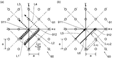
- light L1 scattered (180 ° scattered) in a direction different by 180 ° from the traveling direction before scattering at one lattice point 911 is the four lattices closest to the lattice point. Since the optical path difference from the light L2 scattered at 180 ° at each point 912 matches the wavelength ⁇ PC in the crystal layer, it is amplified by interference (FIG. 1A).
- the light with the wavelength ⁇ PC in the crystal layer propagating in the two-dimensional photonic crystal layer is also scattered at a lattice point 91 in a direction having an angle with respect to the layer.
- such scattered light has an optical path difference of ⁇ PC / 2 between the light scattered at the lattice point 911 and the light scattered at the lattice point 912 (light L5 and light L6 in FIG. 1B), Since the two phases are shifted by 180 °, they cancel each other. Therefore, light is not emitted outside the two-dimensional photonic crystal layer.
- the basic two-dimensional lattice is a square lattice
- the basic two-dimensional lattice is a triangular lattice (hexagonal lattice)
- the light amplified by the interference is scattered (120 ° scattered) in a direction different from the traveling direction before scattering in the lattice plane by 120 °. Except for certain points, this is the same as the case of the square lattice.
- the reciprocal lattice vector G ′ (g ′ x , g ′ y ) is ... (3) It is.
- the reciprocal lattice vector G ′ (g ′ x , g ′ y ) is ...(Four) Or ...(Five) Any combination of these can be used.
- the displacement vector ⁇ r ⁇ at each lattice point of the basic unit cell can be obtained.
- the configuration of the photonic crystal laser according to the present invention has been described. According to this configuration, since the different refractive index regions are two-dimensionally arranged, the different refractive index regions are within the annular range. Since the range in which the light can be amplified can be made wider than that of the conventional photonic crystal laser arranged only, the output can be increased. Further, since the different refractive index regions are two-dimensionally arranged, local laser oscillation is less likely to occur, and a more complete radially polarized annular laser beam can be obtained.
- the light emitting layer is an active layer that emits light when a current is injected, which is typically widely used in conventional lasers, but includes light of wavelength ⁇ L
- the active layer is not limited to such an active layer as long as it generates light.
- the different refractive index region can be formed by providing a hole in the base material.
- the base material may be formed by embedding a member having a refractive index different from that of the base material.
- the planar shape of the different refractive index region may take various shapes such as a circle, a triangle, and other polygons, but it has good symmetry in order to make the cross section of the laser beam more uniform in the circumferential direction of the ring. It is desirable to make it circular. In terms of good symmetry, a hexagon or more polygon may be used instead of a circle.
- the present invention realizes a photonic crystal laser capable of obtaining annular laser beams having various polarizations, such as a larger-diameter polarized annular laser beam having a larger output than the conventional one.
- FIG. 1 is a schematic configuration diagram showing an embodiment of a photonic crystal laser according to the present invention.
- the top view which shows the two-dimensional photonic crystal layer in the photonic crystal laser of this embodiment.
- the elements on larger scale which show the square lattice which is a basic two-dimensional lattice in the dimensional photonic crystal layer of the photonic crystal laser of this embodiment, and the gravity center of a hole.
- FIG. The photograph which shows the spot of a laser beam about three examples from which the direction of inclination
- a radial direction annular laser beam is obtained in the photonic crystal laser of this embodiment.
- the SEM photograph which shows an example of the produced two-dimensional photonic crystal layer about the photonic crystal laser of this embodiment.
- Embodiments of the photonic crystal laser according to the present invention will be described with reference to FIGS.
- FIG. 2 is a perspective view of the photonic crystal laser 10 of the present embodiment.
- the photonic crystal laser 10 includes a lower electrode 151, a lower substrate 141, a lower cladding layer 131, a two-dimensional photonic crystal layer 11, an active layer (light emitting layer) 12, an upper cladding layer 132, and an upper substrate. 142 and the upper electrode 152 are laminated in this order. However, the order of the two-dimensional photonic crystal layer 11 and the active layer 12 may be reversed from the above. In FIG. 2, the two-dimensional photonic crystal layer 11 and the active layer 12 are shown apart from each other in order to show the configuration of the two-dimensional photonic crystal layer 11, but they are actually in contact with each other.
- the lower substrate 141 and the lower electrode 151 are in contact with each other.
- the terms “upper” and “lower” are used for convenience, but these terms do not define the direction (up and down) when the photonic crystal laser is actually used.
- a member such as a spacer may be inserted between the two-dimensional photonic crystal layer 11 and the active layer 12.
- the active layer 12 corresponds to the light emitting layer, and when charge is injected by passing a current between the lower electrode 151 and the upper electrode 152, a predetermined wavelength range corresponding to the material of the active layer 12 Emits light of a certain wavelength.
- a layer having a multiple quantum well (MQW) made of indium gallium arsenide / gallium arsenide (InGaAs / GaAs) can be used as the active layer 12 .
- the active layer 12 emits light having a wavelength in the range of 960 to 990 nm.
- a p-type semiconductor is used for the lower cladding layer 131 and the lower substrate 141, and an n-type semiconductor is used for the upper cladding layer 132 and the upper substrate 142.
- the lower substrate 141 is made of p-type semiconductor gallium arsenide (GaAs)
- the upper substrate 142 is made of n-type GaAs
- the lower clad layer 131 is made of p-type semiconductor aluminum gallium arsenide (AlGaAs)
- AlGaAs aluminum gallium arsenide
- Each of the n-type AlGaAs layers 132 can be used.
- an n-type semiconductor may be used for the lower cladding layer 131 and the lower substrate 141
- a p-type semiconductor may be used for the upper cladding layer 132 and the upper substrate 142.
- the upper electrode 152 is provided with a window (cavity) 1521 provided at the center of a film made of metal such as gold.
- the laser beam generated by the photonic crystal laser 10 is emitted out of the photonic crystal laser 10 through the window 1521.
- a transparent electrode made of ITO (indium tin oxide) or the like may be used instead of the one having the window 1521.
- the lower electrode 151 uses a metal film such as gold having a smaller area than the window 1521 of the upper electrode 152.
- the shape of the lower electrode 151 is circular in this embodiment, but is not particularly limited.
- the two-dimensional photonic crystal layer 11 has holes (different refractive index regions) 111 arranged in a plate-like base material (slab) 112 as described later.
- p-type GaAs is used as the material of the base material 112.
- the shape of the air holes 111 is circular in this embodiment.
- FIG. 3 is a top view of the two-dimensional photonic crystal layer 11.
- holes 111 actually provided in the two-dimensional photonic crystal layer 11 are shown by solid lines, and square lattices that are basic two-dimensional lattices are shown by alternate long and short dash lines, and virtual lattice points of the square lattices are virtually displayed.
- a state where the center of gravity of the hole 111V is arranged is indicated by a broken line.
- an origin 1131 serving as a reference when determining the position of the hole 111 is indicated by a cross
- a reference line 1132 that is a straight line extending in one direction from the origin is indicated by a solid line with an arrow.
- the origin 1131 is an arbitrary one of the lattice points of the basic two-dimensional lattice
- the reference line 1132 is a line parallel to one of the lattice lines orthogonal to each other of the square lattice.
- FIG. 4 shows only a square lattice (dashed line), the center of gravity 111G (black circle) of the hole 111, the origin 1131 and the reference line 1132.
- the volume ratio (filling factor) occupied by the holes 111 in the two-dimensional photonic crystal layer 11 and the refractive index of the base material 112 may be determined.
- the effective refractive index n eff of the two-dimensional photonic crystal layer 11 is 3.4.
- the azimuth angle ⁇ at each lattice point is represented by an angle formed by a straight line connecting the origin 1131 and the lattice point with respect to the reference line 1132 (FIG. 4).
- the reciprocal lattice vector G ′ ⁇ for each lattice point is obtained by substituting the value of the effective refractive index n eff and the azimuth angle ⁇ at the lattice point into the equation (2) because the basic two-dimensional lattice is a square lattice. .
- the value of d in the equation (1) is arbitrary.
- the direction of the displacement vector ⁇ r ⁇ is generally a vector (cos (L ( ⁇ + ⁇ 0 )), sin (L ( ⁇ + ⁇ 0 ))), and in this embodiment, the vector (cos ( ⁇ + ⁇ / 2), sin ( ⁇ + ⁇ / 2)). Therefore, in this embodiment, the center of gravity 111G of the hole 111 is arranged at a position shifted in the direction rotated by ( ⁇ + ⁇ / 2) radians, that is, ( ⁇ + 90) °, from the direction of the reference line at each lattice point. (FIG. 3 (b)).
- a center of gravity 111G is arranged. The direction of these deviations is a direction perpendicular to a straight line connecting the origin and the lattice point.
- the distance of the deviation of the center of gravity 111G of the hole 111 from the lattice point is determined by d sin (G ′ ⁇ ⁇ r ⁇ ). Since G ′ ⁇ and r ⁇ are different vectors for each lattice point, the distance from the lattice point is also different for each lattice point.
- the laser beam generated by the photonic crystal laser 10 becomes a radially polarized annular laser beam by disposing the holes 111 at the respective lattice points at positions shifted from the lattice points as described above. The reason will be described below.
- the direction of displacement of the air holes 111 is the y direction in FIG. 5A, the + 45 ° direction with respect to the x direction in FIG. 5B, and the x direction in FIG.
- These examples are all the same as the example described in Patent Document 2.
- the laser beam having linearly polarized light in the x direction in (a), the + 45 ° direction in the y direction in (b), and the y direction in (c) with respect to the direction of deviation of the holes 111.
- the direction is + 90 ° with respect to the direction of displacement of the holes 111 (lower diagram in FIG. 5).
- the direction of shifting the holes 111 from the lattice points is the same (here, the x direction) at all lattice points, and the magnitude of the displacement is Result of photographing the obtained laser beam with a cross section parallel to the two-dimensional photonic crystal layer when the angle ⁇ in the factor d sin ( ⁇ G ′ ⁇ ⁇ r ⁇ + ⁇ 0 ) is different (the angle ⁇ is the same) Is shown in FIG.
- the two-dimensional photonic crystal layer when the azimuth angle ⁇ in the factor d sin ( ⁇ G ′ ⁇ ⁇ r ⁇ + ⁇ 0 ) is (a) 0 °, (b) 45 °, (c) 90 ° It can be seen that a laser beam having an inclination angle of ⁇ and an azimuth angle of ⁇ with respect to the normal line is emitted.
- the spot 202 of the laser beam in the cross section appears in the direction with the azimuth angle ⁇ of 45 °, and the polarization is 45 ° with respect to the x direction.
- the azimuth angle ⁇ is 90 ° (FIG. 6 (c))
- the direction of displacement of the hole 111 is the x direction (180 °, FIG. 5 (c))
- the laser beam in the cross section is
- the spot 203 appears in the direction in which the azimuth angle ⁇ is 90 °, and its polarization is in the y direction (90 °).
- the polarized light is in the same direction as the direction connecting the origin and the spot.
- a laser beam having an annular cross section is formed (broken line in FIG. 7). Further, by making the direction in which the holes 111 deviate from the lattice points be 90 ° with respect to the direction connecting the origin and the spot, the direction of polarization in each spot is the same as the direction connecting the origin and the spot, that is, It becomes radial direction. That is, by combining these conditions, a radially polarized annular laser beam can be obtained.
- the photonic crystal laser 10 of the present embodiment changes the value of the azimuth angle ⁇ in the equations (1) and (2) within a range of 0 ° to 360 ° for each lattice point, and the positional deviation vector ⁇ r ⁇ .
- the vector cos ( ⁇ + ⁇ / 2), sin ( ⁇ + ⁇ / 2)
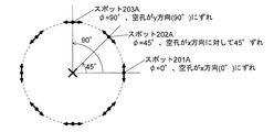
- the laser beam spot 201A appears in the direction where the azimuth angle ⁇ is 0 °, the polarized light becomes y-polarized light (90 °), the azimuth angle ⁇ is 45 ° (FIG. 6B), and the direction of deviation of the holes 111 is If the direction is 45 ° with respect to the x direction (FIG. 5B), the laser beam spot 202A appears in a direction with an azimuth angle ⁇ of 45 °, and the polarization becomes 135 ° with respect to the x direction.
- the laser beam spot 203A has an azimuth angle ⁇ of 90 °. Appears in the direction and becomes x-polarized light (180 °). Therefore, when laser beam spots having different azimuth angles ⁇ within the range of 0 ° to 360 ° are collected, a laser beam having an annular cross section is formed (broken line in FIG. 8). The direction of polarization is the circumferential direction of the ring. Therefore, the laser beam obtained in this example is an azimuthally polarized annular laser beam.
- an annular laser beam having a polarization corresponding to the value of L can be obtained.
- the polarization is the x direction as in FIG. 7, and this direction is the radial direction.
- the direction of polarization rotates by 2 ⁇ .
- the photograph of the cross section of the laser beam obtained with the laser 10 is shown.
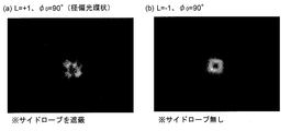
- the spread angle ⁇ was set to 1 ° in all cases. In either case, a laser beam having an annular cross section is obtained. Note that, under the condition (a), light emission (side lobe) also appeared outside the ring of the cross section, so FIG. 10 (a) shows a photograph in which the side lobe is shielded. In (b), no side lobe appeared.
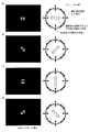
- the direction of polarized light that can pass through the polarizing element is indicated by a white arrow corresponding to each of the four photographs, and designed at each position of the annular cross section of the laser beam (L And the direction of polarized light assumed from the values of ⁇ 0 are indicated by black arrows.
- a portion in which the direction of polarized light that can pass through the polarizing element and the assumed direction of polarized light coincide with each other is surrounded by a broken line.
- the position of the portion where the light appears in the left photograph coincides with the position of the portion surrounded by the broken line in the right view. From this result, it can be said that an annular laser beam having the designed polarization is obtained.
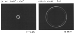
- the divergence angle ⁇ was set to be 1 ° in (a) and 8 ° in (b).
- the filling factor (FF) was 12.0% in (a) and 14.0% in (b).
- the other parameters were common to (a) and (b), the lattice constant a was 206 nm, and the diameter of the lower electrode 151 and the thickness of each layer were also common.
- (A) and (b) of FIG. 13 are represented by the same scale, and it can be seen that the ring diameter is smaller when the spread angle ⁇ is smaller (a).
- FIG. 14 is an SEM photograph showing an example of the two-dimensional photonic crystal layer 11 produced for the photonic crystal laser 10 of the present embodiment.
- Each hole 111 is arranged at a position shifted from the lattice point of the square lattice, and the direction and size of the shift are different for each hole 111.
- the shape of the hole (different refractive index region) 111 is circular, but it can be various shapes such as a regular triangle, other triangles, a polygon including a triangle, and an ellipse.
- a member having a refractive index different from that of the base material 112 may be used instead of the holes 111.
- the holes are excellent in that they can be easily processed, whereas the different refractive index member is advantageous when the base material may be deformed by heating during processing.
- the basic two-dimensional lattice is not limited to a square lattice, and a triangular lattice, a rectangular lattice, or the like may be used.
- a triangular lattice or a rectangular lattice is used, the displacement vector ⁇ r ⁇ obtained by substituting the reciprocal lattice vector G ' ⁇ shown in any of equations (3) to (5) into equation (1) It is sufficient to set the position of the different refractive index region by using it.
- the photonic crystal laser according to the present invention can obtain an annular laser beam having a desired polarization distribution, and can resonate in a large area and has an oscillation mode called a TE mode, so that the output can be increased. Is possible. Due to these excellent features, the photonic crystal laser according to the present invention can be suitably used for many devices such as a high-resolution microscope, various measuring instruments / analyzers, laser processing machines, OCT diagnostic apparatuses and the like.
Landscapes
- Physics & Mathematics (AREA)
- Condensed Matter Physics & Semiconductors (AREA)
- General Physics & Mathematics (AREA)
- Electromagnetism (AREA)
- Optics & Photonics (AREA)
- Semiconductor Lasers (AREA)
- Optical Integrated Circuits (AREA)
Abstract
フォトニック結晶レーザ10は、波長λLの光を含む光を生じさせる発光層(活性層12)と、板状の母材112に、それとは屈折率が異なる異屈折率領域(空孔111)が2次元的に配置されることにより屈折率分布が形成されて成る2次元フォトニック結晶層11とが積層された構成を有するレーザであって、2次元フォトニック結晶層11において各異屈折率領域が、2次元定在波を形成することによって前記波長λLの光の共振状態を形成し且つ該波長λLの光を外部に出射させないように定められる周期性を持つ基本2次元格子の各格子点からずれた位置に配置されており、前記各格子点における異屈折率領域の位置の、該格子点からのずれを表す位置ずれベクトルΔr↑が、2次元フォトニック結晶層11内における前記波長λLの光の波数ベクトルk↑=(kx, ky)、前記2次元フォトニック結晶層の有効屈折率neff、前記基本2次元格子の所定の原点から所定の方向に延びる所定の基準線からの方位角φ、任意の定数φ0、及びレーザビームの拡がり角θを用いて表される逆格子ベクトルG'↑=±(kx±|k↑|(sinθcosφ)/neff, ky±|k↑|(sinθsinφ)/neff)、前記各格子点の位置ベクトルr↑、任意の定数d及びψ0、並びに0を除く整数Lを用いて、 Δr↑=d・sin(±G'↑・r↑+ψ0)・(cos(L(φ+φ0)), sin(L(φ+φ0))) で表される。
Description
本発明は、集積回路等を作製する際の微細な加工や、微小な試料の検出に用いるスポット径の小さいレーザを生成するのに適したフォトニック結晶レーザに関する。
微細な加工や微小な試料の検出に用いる光源では、それら加工や検出の精度を高めるために、レーザビームをできるだけ小さい点に集光することが求められている。しかし、単に集光レンズでレーザビームを集光するだけでは、レーザビームのスポット径の大きさは、レーザの波長及び集光レンズの開口数により決定される回折限界値以下にすることはできない。
特許文献1には、スポット径を小さくすることに適したレーザビームを生成するものであって、活性層とフォトニック結晶を有するレーザ(フォトニック結晶レーザ)が記載されている。フォトニック結晶レーザでは、活性層に電流が注入されることによって生成される光のうち、フォトニック結晶の屈折率の周期に応じた特定の波長の光のみが干渉により選択的に増幅され、レーザ発振する。このフォトニック結晶における屈折率の周期は、一般に、光の波長と同程度となっている。特許文献1に記載のフォトニック結晶レーザでは、フォトニック結晶は、板状の母材内に、該母材とは屈折率が異なる領域である異屈折率領域が環状に、該環の周方向に周期的に並ぶように配置されている。各異屈折率領域は、その中心を通り前記環の径方向に延びる軸に関して非対称な形状を有している。このようなフォトニック結晶を有することにより、特許文献1に記載のフォトニック結晶レーザは、図15(a)に示すように、断面81が環状であって環の径方向(同図中に矢印で示す方向)に偏光したレーザビームを発振する。以下、このようなレーザビームを「径偏光環状レーザビーム」と呼ぶ。
このような径偏光環状レーザビームを集光することにより、焦点の近傍で光軸方向の電界が生成され、ビーム径が回折限界値よりも小さいレーザビームが得られる。従来、小さなビーム径は光軸方向に1波長程度のごく狭い(短い)領域においてしか得られなかったが、径偏光環状レーザビームを用いることにより10波長以上の長い領域において得ることができる。
また、図15(b)に示すように、径偏光環状レーザビームをレンズ83で集光すると、レーザビームの環状部分が屈折する際に径偏光の電界に、レーザビームに平行な方向(z方向)の成分が生じる。このような成分を有する偏光を用いると、例えばラマン散乱測定において、レーザビームに垂直な偏光を用いた場合には生じなかった散乱を観測することができる、という利点がある(非特許文献1参照)。
「Z偏光素子」、[online]、2005年、ナノフォトン株式会社、[2017年2月13日検索]、インターネット<URL:http://www.nanophoton.jp/products/zpol/index.html>
特許文献1に記載のフォトニック結晶レーザでは、板状の母材内に異屈折率領域が環状に並んで配置されたフォトニック結晶を用いているため、活性層で生成された光は、母材のうち、当該環状の部分においてのみ増幅される。そのため、特許文献1に記載のフォトニック結晶レーザでは、出力を大きくすることが難しい。また、このフォトニック結晶レーザでは、共振器長が長くなるため、異屈折率領域が配置された環状の部分のうちの一部でのみレーザ発振が生じて均一性が損なわれてしまい、完全な径偏光環状レーザビームを得ることができないことがある。
本発明が解決しようとする課題は、従来よりも出力が大きく且つより完全な径偏光環状レーザビーム等の、種々の偏光を有する環状レーザビームを得ることができるフォトニック結晶レーザを提供することである。
最近、板状の母材に該母材とは屈折率が異なる異屈折率領域が2次元格子(正方格子、三角格子等)状に配置された2次元フォトニック結晶を有するフォトニック結晶レーザが提案されている。このフォトニック結晶レーザにおいて、異屈折率領域を、活性層で生じる所定の波長に対応して定まる所定の周期を有する2次元格子の格子点から特定の1方向にずれた位置に配置し、そのずれの大きさを格子点の位置に応じて周期的に変化させておくことにより、該1方向に垂直な方向の直線偏光を有し、母材の面の法線に対して傾斜した方向に出射するレーザビームが得られることが明らかになった(特許文献2)。但し、このフォトニック結晶レーザで得られるレーザビームの断面は環状ではなく、偏光は前述の通り直線偏光であって、径偏光ではない。本発明者は、このフォトニック結晶レーザにおいて、異屈折率領域を格子点から特定の1方向にずらして配置する代わりに、格子点毎に異なる方向に(2次元的に)ずらすことにより、径偏光等の様々な形態の偏光を有するレーザビームが得られることを見出した。また、格子点からのずれの大きさを、格子点の位置に応じて周期的に変化させるのに加えてさらに変化させておくことにより、環状のレーザビームが得られることを見出した。これらの知見により、本発明が完成した。
すなわち、本発明に係るフォトニック結晶レーザは、
波長λLの光を含む光を生じさせる発光層と、板状の母材に、該母材とは屈折率が異なる異屈折率領域が2次元的に配置されることにより屈折率分布が形成されて成る2次元フォトニック結晶層とが積層された構成を有するレーザであって、
該2次元フォトニック結晶層において各異屈折率領域が、2次元定在波を形成することによって前記波長λLの光の共振状態を形成し且つ該波長λLの光を外部に出射させないように定められる周期性を持つ基本2次元格子の各格子点からずれた位置に配置されており、
前記各格子点における異屈折率領域の位置の、該格子点からのずれの大きさが、前記基本2次元格子の所定の原点から径方向及び周方向に向かってそれぞれ所定の周期で変化する変調を有し、該格子点からのずれの方向が、該原点と該格子点を結ぶ直線の方向によって異なる
ことを特徴とする。
波長λLの光を含む光を生じさせる発光層と、板状の母材に、該母材とは屈折率が異なる異屈折率領域が2次元的に配置されることにより屈折率分布が形成されて成る2次元フォトニック結晶層とが積層された構成を有するレーザであって、
該2次元フォトニック結晶層において各異屈折率領域が、2次元定在波を形成することによって前記波長λLの光の共振状態を形成し且つ該波長λLの光を外部に出射させないように定められる周期性を持つ基本2次元格子の各格子点からずれた位置に配置されており、
前記各格子点における異屈折率領域の位置の、該格子点からのずれの大きさが、前記基本2次元格子の所定の原点から径方向及び周方向に向かってそれぞれ所定の周期で変化する変調を有し、該格子点からのずれの方向が、該原点と該格子点を結ぶ直線の方向によって異なる
ことを特徴とする。
前記所定の原点は、任意の値を1つずつ定めればよい。また、前記径方向に向かって変化する変調の所定の周期と、前記周方向に向かって変化する変調の所定の周期はそれぞれ、任意の値を1つずつ定めればよい。
本発明に係るフォトニック結晶レーザは、以下のように表すこともできる。すなわち、本発明に係るフォトニック結晶レーザは、
波長λLの光を含む光を生じさせる発光層と、板状の母材に、該母材とは屈折率が異なる異屈折率領域が2次元的に配置されることにより屈折率分布が形成されて成る2次元フォトニック結晶層とが積層された構成を有するレーザであって、
該2次元フォトニック結晶層において各異屈折率領域が、2次元定在波を形成することによって前記波長λLの光の共振状態を形成し且つ該波長λLの光を外部に出射させないように定められる周期性を持つ基本2次元格子の各格子点からずれた位置に配置されており、
前記各格子点における異屈折率領域の位置の、該格子点からのずれを表す位置ずれベクトルΔr↑が、前記2次元フォトニック結晶層内における前記波長λLの光の波数ベクトルk↑=(kx, ky)、前記2次元フォトニック結晶層の有効屈折率neff、前記基本2次元格子の所定の原点から所定の方向に延びる所定の基準線からの方位角φ、任意の定数φ0、及びレーザビームの拡がり角θを用いて表される逆格子ベクトルG'↑=±(kx±|k↑|(sinθcosφ)/neff, ky±|k↑|(sinθsinφ)/neff)、前記各格子点の位置ベクトルr↑、任意の定数d及びψ0、並びに0を除く整数Lを用いて、
Δr↑=d・sin(±G'↑・r↑+ψ0)・(cos(L(φ+φ0)), sin(L(φ+φ0))) …(1)
で表されることを特徴とする。
波長λLの光を含む光を生じさせる発光層と、板状の母材に、該母材とは屈折率が異なる異屈折率領域が2次元的に配置されることにより屈折率分布が形成されて成る2次元フォトニック結晶層とが積層された構成を有するレーザであって、
該2次元フォトニック結晶層において各異屈折率領域が、2次元定在波を形成することによって前記波長λLの光の共振状態を形成し且つ該波長λLの光を外部に出射させないように定められる周期性を持つ基本2次元格子の各格子点からずれた位置に配置されており、
前記各格子点における異屈折率領域の位置の、該格子点からのずれを表す位置ずれベクトルΔr↑が、前記2次元フォトニック結晶層内における前記波長λLの光の波数ベクトルk↑=(kx, ky)、前記2次元フォトニック結晶層の有効屈折率neff、前記基本2次元格子の所定の原点から所定の方向に延びる所定の基準線からの方位角φ、任意の定数φ0、及びレーザビームの拡がり角θを用いて表される逆格子ベクトルG'↑=±(kx±|k↑|(sinθcosφ)/neff, ky±|k↑|(sinθsinφ)/neff)、前記各格子点の位置ベクトルr↑、任意の定数d及びψ0、並びに0を除く整数Lを用いて、
Δr↑=d・sin(±G'↑・r↑+ψ0)・(cos(L(φ+φ0)), sin(L(φ+φ0))) …(1)
で表されることを特徴とする。
(1)式中のsin(±G'↑・r↑+ψ0)は、前述の基本2次元格子の所定の原点から径方向に向かって所定の周期で変化する変調を表している。また、(1)式中のφ0は前記所定の角度に該当する。
前記波長λLは、真空中における波長で定義する。波長λLの光は、2次元フォトニック結晶層内では波長がλL/neffとなる。有効屈折率neffは、上記各層が積層した構造において2次元フォトニック結晶層に分布する光の電界強度の割合、及び母材に対する異屈折率領域の充填率を考慮した屈折率である。なお、本発明に係るフォトニック結晶レーザは、上記発光層及び上記2次元フォトニック結晶層の他に、クラッド層やスペーサ層等を有していてもよい。
上記本発明に係るフォトニック結晶レーザにおいて、径偏光環状レーザビームを出射するためには、(1)式中のLの値を+1、φ0の値を90°とする。
一方、(1)式中のLの値を+1、φ0を0°とすれば、レーザビームの断面において環の周方向に偏光した方位偏光環状レーザビームが得られる。さらに、径偏光及び方位偏光以外にも、Lの値を適宜設定することにより、環の周方向に(360/L)°回転する毎に同方向となる偏光を有する環状レーザビームが得られる。このような様々な偏光を有する環状レーザビームは、それを集光して形成される集光場により微小な物体を保持する光ピンセットとして用いたり、集光場により高密度にデータを記録する光記録装置の光源として用いたり、高分解能で観察が可能な顕微鏡の光源として用いたり、光造形等の用途に用いることができる。
本発明では、基本2次元格子は次段落以降で説明するように、波長λLの光の共振状態を形成し且つ該波長λLの光を外部に出射させない構造を有している。これにより、波長は所定値λLであるものの所定の偏光を有しないレーザビームや断面が環状ではないレーザビームがフォトニック結晶レーザから出射することを防止する。それと共に、異屈折率領域が格子点から、前記基本2次元格子の所定の原点から径方向に向かって所定の周期で変化する変調を有する大きさで、該原点と該格子点を結ぶ直線と所定の角度を成す方向(各格子点から位置ずれベクトルΔr↑で表される位置)にずれていることにより、径偏光環状レーザビームが出射する。以下、(a)異屈折率領域の格子点からの位置ずれ、及び(b)基本2次元格子について詳細に説明する。
(a)異屈折率領域の格子点からの位置ずれ
特許文献2のフォトニック結晶レーザでは、位置ベクトルr↑で位置が表される基本2次元格子の各格子点において、格子点からd sin(G'↑・r↑)の距離だけ1方向にずれた位置に異屈折率領域を配置している。ここで距離d sin(G'↑・r↑)は、基本2次元格子の所定の原点から径方向に向かって所定の周期で変化する変調を表している。但し、周方向には所定の周期の変化を有しない。また、距離d sin(G'↑・r↑)に含まれる角度θは、特許文献2では母材の法線に対するレーザビームの傾斜角を表し、角度φはレーザビームの方位角を示している。これにより、特許文献2のフォトニック結晶レーザでは、前記1方向に垂直な方向の直線偏光を有し、母材の面の法線に対して傾斜角θで傾斜したレーザビームが、方位角φの方向に出射する。一方、特許文献2のフォトニック結晶レーザでは、上記のように異屈折率領域が格子点から1方向にずれており、ずれの方向が原点と格子点を結ぶ直線と所定の角度を成すという構成は取っていない。
特許文献2のフォトニック結晶レーザでは、位置ベクトルr↑で位置が表される基本2次元格子の各格子点において、格子点からd sin(G'↑・r↑)の距離だけ1方向にずれた位置に異屈折率領域を配置している。ここで距離d sin(G'↑・r↑)は、基本2次元格子の所定の原点から径方向に向かって所定の周期で変化する変調を表している。但し、周方向には所定の周期の変化を有しない。また、距離d sin(G'↑・r↑)に含まれる角度θは、特許文献2では母材の法線に対するレーザビームの傾斜角を表し、角度φはレーザビームの方位角を示している。これにより、特許文献2のフォトニック結晶レーザでは、前記1方向に垂直な方向の直線偏光を有し、母材の面の法線に対して傾斜角θで傾斜したレーザビームが、方位角φの方向に出射する。一方、特許文献2のフォトニック結晶レーザでは、上記のように異屈折率領域が格子点から1方向にずれており、ずれの方向が原点と格子点を結ぶ直線と所定の角度を成すという構成は取っていない。
それに対して、本発明に係るフォトニック結晶レーザでは、各格子点における該格子点からの異屈折率領域のずれの大きさは、基本2次元格子の所定の原点から径方向に向かって所定の周期で変化すると共に、周方向に向かっても所定の周期(径方向の周期と同じである必要はない)で変化する。これにより、得られるレーザビームの断面の形状は環状となる。(1)式でいうと、位置ずれベクトルΔr↑が、ずれの大きさを表す因子d sin(±G'↑・r↑+ψ0)にずれの方向を表すベクトル(cos(L(φ+φ0)), sin(L(φ+φ0)))を乗じたものであって、原点からの距離を表す|r↑|及び周方向の変化を表す方位角φをそれぞれ変化させていくと、ずれの大きさを表す因子d sin(±G'↑・r↑+ψ0)は周期的に変化する。一方、位置ずれベクトルΔr↑に含まれる角度θは格子点に依らない定数であり、前述の基本2次元格子の所定の原点から径方向及び周方向に向かってそれぞれ所定の周期で変化する変調においても対応する定数が規定できる。これにより、生成されるレーザビームは、傾斜角θを有する直線を母材の面の法線の周りに回転させて成る円錐面状の形状となる。この形状のレーザビームの断面は環状である。なお、この環状のレーザビームは、フォトニック結晶レーザから離れるに従って角度θで拡がってゆき、径が大きくなるが、θを十分に小さい値に設定することにより、この拡がりを抑えることができる。
また、各格子点における該格子点からの異屈折率領域のずれの方向が、該原点と該格子点を結ぶ直線の方向によって異なることにより、得られるレーザビームの環内での位置によって方向が異なる偏光が得られる。(1)式でいうと、位置ずれベクトルΔr↑におけるずれの方向を表すベクトル(cos(L(φ+φ0)), sin(L(φ+φ0)))が(360/L)°の周期を有することにより、レーザビームの断面において、環の周方向に(360/L)°の周期で直線偏光の方向が1回転する偏光が得られる。例えばL=±1の場合には、環の周方向に360°(つまり1周)進む毎に偏光が1回転する。ここでL=+1の場合においてφ0=90°とすると、直線偏光の方向が環の周方向の位置に依らずに径方向となり、径偏光のレーザビームが得られる。また、L=+1の場合においてφ0=0とすると、直線偏光の方向が環の周方向の位置に依らずに周方向となり、方位偏光の環状レーザビームが得られる。
以上のように、本発明に係るフォトニック結晶レーザでは、断面が環状であって、環の周方向に(360/L)°の周期で直線偏光の方向が1回転する偏光を有するレーザビームが得られる。そして、L=+1、φ0=90°の場合に径偏光環状レーザビームが得られ、L=+1、φ0=0の場合に方位偏光環状レーザビームが得られる。
なお、特許文献3には、フォトニック結晶レーザにおいて、共振状態形成用格子点に摂動が加えられていることが記載されている。しかし、特許文献3における摂動は、異屈折率領域(空孔)の平面形状の大きさや深さを異屈折率領域毎に異なるものとしたり、共振状態形成用の格子に別の格子である摂動状態形成用格子を重畳するものであって、異屈折率領域の位置を格子点からずらすことは記載されていない。また、特許文献3には、断面形状が環状であるレーザビームが得られることも、偏光に関することも記載されていない。
(b)基本2次元格子
基本2次元格子、すなわち波長λLの光の共振状態を形成し且つ該波長λLの光を外部に出射させない2次元格子は、従来より知られているものである。基本2次元格子の例の1つとして、格子定数aが
a=2-1/2λL/neff=2-1/2λPC
である正方格子が挙げられる。また、格子定数a1及びa2が
(1/2)×(a1 -2+a2 -2)1/2=1/λPC
の関係式を満たす長方格子(面心長方格子を含む)や、格子定数aが
a=(2/3)λPC
である三角格子も、前記基本2次元格子の例として挙げられる。
基本2次元格子、すなわち波長λLの光の共振状態を形成し且つ該波長λLの光を外部に出射させない2次元格子は、従来より知られているものである。基本2次元格子の例の1つとして、格子定数aが
a=2-1/2λL/neff=2-1/2λPC
である正方格子が挙げられる。また、格子定数a1及びa2が
(1/2)×(a1 -2+a2 -2)1/2=1/λPC
の関係式を満たす長方格子(面心長方格子を含む)や、格子定数aが
a=(2/3)λPC
である三角格子も、前記基本2次元格子の例として挙げられる。
このような基本2次元格子が波長λLの光を増幅し且つ該波長λLの光を外部に出射させない理由を、上記の式a=2-1/2λPCを満たす正方格子の場合を例に、図1を用いて説明する。
2次元フォトニック結晶層内では、基本2次元格子90の正方格子の格子点91に異屈折率領域が配置されていると、結晶層内波長λPCの光が様々な方向に散乱される。それら散乱光のうち、ある1個の格子点911において、散乱前の進行方向とは180°異なる方向に散乱(180°散乱)された光L1は、その格子点に最隣接の4個の格子点912においてそれぞれ180°散乱された光L2との光路差が結晶層内波長λPCに一致するため、干渉により増幅される(図1(a)。この図では、1個の格子点912に散乱された光L2のみを示す。)。また、格子点911において格子面内で散乱前の進行方向とは90°異なる方向に散乱(90°散乱)された光L3は、4個の格子点912においてそれぞれ格子面内で90°散乱された光L4との光路差が結晶層内波長λPCに一致するため、干渉により増幅される(図1(a))。このように、180°散乱と90°散乱の双方によって2次元定在波が形成され、光が増幅される。
一方、2次元フォトニック結晶層内を伝播する結晶層内波長λPCの光は、格子点91において、該層に対して角度をもった方向にも散乱される。しかしながら、このような散乱光は、格子点911において散乱されるものと、格子点912において散乱されるものの光路差がλPC/2になり(図1(b)の光L5と光L6)、両者の位相が180°だけずれるため、打ち消し合う。そのため、光は2次元フォトニック結晶層の外部に出射されない。
なお、ここでは基本2次元格子が正方格子の場合を例に説明したが、長方格子においても同様である。基本2次元格子が三角格子(六方格子)の場合には、干渉により増幅される光が、格子面内で散乱前の進行方向とは120°異なる方向に散乱(120°散乱)された光である点を除いて、正方格子の場合と同様である。
基本2次元格子が格子定数aの正方格子である場合には、逆格子ベクトルG'↑(=(g'x, g'y)とする)は、

…(2)
である。また、基本2次元格子が格子定数a1, a2の長方格子の場合には、逆格子ベクトルG'=(g'x, g'y)は、

…(3)
である。一方、基本2次元格子が格子定数aの三角格子の場合には、逆格子ベクトルG'=(g'x, g'y)は、

…(4)
又は、

…(5)
のいずれかの組み合わせを用いることができる。これら各基本単位格子における逆格子ベクトルG'を(1)式に代入することにより、当該基本単位格子の各格子点における位置ずれベクトルΔr↑を求めることができる。
…(2)
である。また、基本2次元格子が格子定数a1, a2の長方格子の場合には、逆格子ベクトルG'=(g'x, g'y)は、
…(3)
である。一方、基本2次元格子が格子定数aの三角格子の場合には、逆格子ベクトルG'=(g'x, g'y)は、
…(4)
又は、
…(5)
のいずれかの組み合わせを用いることができる。これら各基本単位格子における逆格子ベクトルG'を(1)式に代入することにより、当該基本単位格子の各格子点における位置ずれベクトルΔr↑を求めることができる。
ここまで、本発明に係るフォトニック結晶レーザの構成を説明したが、この構成によれば、異屈折率領域が2次元的に配置されていることにより、異屈折率領域が環状の範囲内にのみ配置された従来のフォトニック結晶レーザよりも光を増幅することができる範囲を広くすることができるため、出力を高くすることができる。また、異屈折率領域が2次元的に配置されていることにより、局所的なレーザ発振が生じ難くなり、より完全な径偏光環状レーザビームを得ることができる。
本発明に係るフォトニック結晶レーザにおいて、発光層は、典型的には従来のレーザで広く用いられている、電流が注入されることにより発光する活性層であるが、波長λLの光を含む光を生じさせるものであれば、このような活性層には限定されない。
前記異屈折率領域には、母材に空孔を設けることにより形成することができる。あるいは、母材に該母材とは異なる屈折率を有する部材を埋め込むことにより形成してもよい。異屈折率領域の平面形状は、円形や三角形その他の多角形等の種々の形状を取り得るが、レーザビームの断面を環の周方向により一様に近くするために、対称性が良いという点で円形とすることが望ましい。対称性が良いという点では、円形の代わりに、六角形以上の多角形としてもよい。
本発明により、従来よりも出力が大きく且つより完全な径偏光環状レーザビーム等の、種々の偏光を有する環状レーザビームを得ることができるフォトニック結晶レーザが実現する。
図2~図14を用いて、本発明に係るフォトニック結晶レーザの実施形態を説明する。
図2は、本実施形態のフォトニック結晶レーザ10の斜視図である。このフォトニック結晶レーザ10は、下部電極151と、下部基板141と、下部クラッド層131と、2次元フォトニック結晶層11と、活性層(発光層)12と、上部クラッド層132と、上部基板142と、上部電極152とを、この順に積層したものである。但し、2次元フォトニック結晶層11と、活性層12の順番は上記のものとは逆であってもよい。なお、図2では2次元フォトニック結晶層11の構成を示すために2次元フォトニック結晶層11と活性層12を離して示しているが、実際には両者は接している。同様に、下部基板141と下部電極151も接している。本願では便宜上、「上」及び「下」という語を用いるが、これらの語は実際にフォトニック結晶レーザを使用する際の向き(上下)を規定するものではない。また、2次元フォトニック結晶層11と活性層12の間には、スペーサ等の部材が挿入されていてもよい。
まず、2次元フォトニック結晶層11以外の各層の構成を説明する。活性層12は、前記発光層に相当するものであり、下部電極151と上部電極152の間に電流を流すことで電荷が注入されると、該活性層12の材料に応じた所定の波長範囲内にある波長の光を発する。活性層12には、例えばインジウム・ガリウムヒ素/ガリウムヒ素(InGaAs/GaAs)から成る多重量子井戸(Multiple-Quantum Well; MQW)を有するものを用いることができる。この活性層12は、960~990nmの範囲内の波長の光を発光する。下部クラッド層131及び下部基板141にはp型半導体を用い、上部クラッド層132及び上部基板142にはn型半導体を用いる。例えば、下部基板141にはp型半導体のガリウムヒ素(GaAs)を、上部基板142にはn型GaAsを、下部クラッド層131にはp型半導体のアルミニウム・ガリウムヒ素(AlGaAs)を、上部クラッド層132にはn型AlGaAsを、それぞれ用いることができる。なお、下部クラッド層131及び下部基板141にn型半導体を用い、上部クラッド層132及び上部基板142にp型半導体を用いてもよい。
上部電極152には、本実施形態では金等の金属から成る膜の中央部に窓(空洞)1521が設けられたものを用いる。フォトニック結晶レーザ10で生成されるレーザビームは、窓1521を通ってフォトニック結晶レーザ10の外に出射する。上部電極152には、窓1521を有するものの代わりに、ITO(インジウム錫酸化物)等から成る透明電極を用いてもよい。下部電極151は、本実施形態では上部電極152の窓1521よりも面積が小さい金等の金属製の膜を用いる。下部電極151の形状は、本実施形態では円形としたが、特に問わない。
次に、2次元フォトニック結晶層11の構成を説明する。2次元フォトニック結晶層11は、図3に示すように、板状の母材(スラブ)112内に空孔(異屈折率領域)111を後述のように配置したものである。本実施例では、母材112の材料にはp型GaAsを用いた。空孔111の形状は、本実施形態では円形とした。
図3及び図4を用いて、母材112内での空孔111の配置を説明する。本実施形態では、基本2次元格子を正方格子とする。図3は2次元フォトニック結晶層11の上面図である。この図には、2次元フォトニック結晶層11に実際に設けられた空孔111を実線で示した他、基本2次元格子である正方格子を一点鎖線で示し、その正方格子の格子点に仮想的に空孔111Vの重心が配置された状態を破線で示す。また、後述のように空孔111の位置を定める際の基準となる原点1131を×印で示し、該原点から1方向に延びる直線である基準線1132を矢印付きの実線で示す。原点1131は、基本2次元格子の格子点のうち任意の1点とし、基準線1132は、正方格子の互いに直交する格子線のうちの一方と平行な線とした。図4には、正方格子(一点鎖線)、空孔111の重心111G(黒丸)、原点1131及び基準線1132のみを示す。
基本2次元格子の格子定数aは、活性層12が発光する960~990nmの波長範囲内から、レーザ発振させる波長λLを選択したうえで、a=2-1/2λL/neffとなるように定めればよい。ここで、2次元フォトニック結晶層11内において空孔111が占める体積の割合(フィリングファクター)と母材112の材料の屈折率に基づいて定めればよい。本実施形態では、2次元フォトニック結晶層11の有効屈折率neffは3.4とした。
本実施形態では、径偏光環状レーザビームを得るために、上記(1)式においてL=+1、φ0=90°とする。また、レーザビームの拡がり角θは任意の値(例えばθ=1°)とする。各格子点における方位角φは、基準線1132に対して、原点1131と該格子点を結ぶ直線が成す角度で表す(図4)。
格子点毎の逆格子ベクトルG'↑は、基本2次元格子が正方格子であることから、(2)式に有効屈折率neff及び該格子点における方位角φの値を代入したものとなる。そして、格子点毎の位置ずれベクトルΔr↑は、(1)式にL=1及びφ0=90°、並びに格子点毎の位置ベクトルr↑及び逆格子ベクトルG'↑を代入したものとなる。なお、(1)式中のdの値は任意である。
(1)式より、位置ずれベクトルΔr↑の方向は、一般にベクトル(cos(L(φ+φ0)), sin(L(φ+φ0)))、本実施形態ではベクトル(cos(φ+π/2), sin(φ+π/2))で定まる。従って、本実施形態では、各格子点において基準線の方向から(φ+π/2)ラジアン、すなわち(φ+90)°回転させた方向にずれた位置に空孔111の重心111Gが配置される(図3(b))。例えば、基準線1132上の格子点(φ=0°)では該基準線1132に垂直な方向に、基準線1132に直交する線1133上の格子点(φ=90°)では基準線1132に平行な方向に、基準線1132とφ=45°の角度で交差する線1134上の格子点では該線1134に直交するφ=135°の方向に、それぞれ格子点からずれた位置に空孔111の重心111Gが配置される。これらのずれの方向はいずれも、原点と格子点を結ぶ直線に対して垂直な方向である。
一方、空孔111の重心111Gの、格子点からのずれの距離はd sin(G'↑・r↑)で定まる。G'↑及びr↑がそれぞれ、格子点毎に異なるベクトルであることから、格子点からのずれの距離も格子点毎に異なる値となる。
各格子点において空孔111が該格子点から上記のようにずれた位置に配置されていることにより、フォトニック結晶レーザ10で生成されるレーザビームは、径偏光環状レーザビームとなる。以下、その理由を説明する。
(a)レーザビームが径偏光になる理由
まず、本実施形態とは異なり、全ての格子点において空孔111を同じ方向にずらした場合について検討する。図5の上段図には、全ての格子点において、空孔111のずれの方向を表すベクトル(cos(L(φ+φ0)), sin(L(φ+φ0)))を格子点毎の方位角φに依存しない
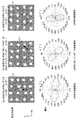
ベクトルに置き換え、ずれの大きさを表す因子d sin(±G'↑・r↑+ψ0)中のθを30°、φを0°、ψ0を0°とした場合の例を示す。空孔111のずれの方向は、図5(a)ではy方向、(b)ではx方向に対して+45°の方向、(c)ではx方向とした。これらの例はいずれも、特許文献2に記載の例と同じである。その結果、空孔111のずれの方向に対して、(a)ではx方向、(b)ではy方向に対して+45°の方向、(c)ではy方向の直線偏光を有するレーザビームが得られ、いずれの例においても空孔111のずれの方向に対して+90°の方向となる(図5の下段図)。
まず、本実施形態とは異なり、全ての格子点において空孔111を同じ方向にずらした場合について検討する。図5の上段図には、全ての格子点において、空孔111のずれの方向を表すベクトル(cos(L(φ+φ0)), sin(L(φ+φ0)))を格子点毎の方位角φに依存しない
ベクトルに置き換え、ずれの大きさを表す因子d sin(±G'↑・r↑+ψ0)中のθを30°、φを0°、ψ0を0°とした場合の例を示す。空孔111のずれの方向は、図5(a)ではy方向、(b)ではx方向に対して+45°の方向、(c)ではx方向とした。これらの例はいずれも、特許文献2に記載の例と同じである。その結果、空孔111のずれの方向に対して、(a)ではx方向、(b)ではy方向に対して+45°の方向、(c)ではy方向の直線偏光を有するレーザビームが得られ、いずれの例においても空孔111のずれの方向に対して+90°の方向となる(図5の下段図)。
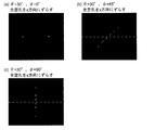
次に、本実施形態及び上記図5の例とは異なり、格子点から空孔111をずらす方向を全ての格子点において同じ(ここではx方向とする)としたうえで、ずれの大きさを表す因子d sin(±G'↑・r↑+ψ0)中の角度φが異なる(角度θは同じ)場合について、得られたレーザビームを2次元フォトニック結晶層に平行な断面で撮影した結果を図6に示す。因子d sin(±G'↑・r↑+ψ0)中の方位角φが(a)0°、(b)45°、(c)90°の場合のいずれにおいても、2次元フォトニック結晶層の法線に対する傾斜角が角度θ、方位角がφであるレーザビームが出射していることがわかる。
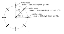
これら図5及び図6の結果を組み合わせると、以下のことがいえる。方位角φが0°(図6(a))であって空孔111のずれの方向がy方向(90°、図5(a))であれば、図7に示すように、2次元フォトニック結晶層に平行な断面におけるレーザビームのスポット201は、方位角φが0°である方向に現れ、その偏光はx方向(0°)になる。同様に、方位角φが45°(図6(b))であって空孔111のずれの方向がx方向に対して135°の方向(図5(b))である場合には、前記断面におけるレーザビームのスポット202は、方位角φが45°である方向に現れ、その偏光はx方向に対して45°の方向になる。また、方位角φが90°(図6(c))であって空孔111のずれの方向がx方向(180°、図5(c))である場合には、前記断面におけるレーザビームのスポット203は、方位角φが90°である方向に現れ、その偏光はy方向(90°)になる。いずれスポットにおいても、偏光は原点とスポットを結ぶ方向と同じ方向となる。
従って、これらのレーザビームのスポットを、方位角φが0°から360°の範囲内で集めると、断面が環状のレーザビームが形成される(図7の破線)。また、空孔111が格子点からずれる方向を、原点とスポットを結ぶ方向に対して90°の方向とすることにより、各スポットにおける偏光の方向は、原点とスポットを結ぶ方向と同じ方向、すなわち径方向となる。つまり、これらの条件を組み合わせることにより、径偏光環状レーザビームが得られる。本実施形態のフォトニック結晶レーザ10は、格子点毎に(1)式及び(2)式における方位角φの値を0°から360°の範囲内で変化させ、且つ、位置ずれベクトルΔr↑の方向を規定するベクトル(cos(φ+π/2), sin(φ+π/2))により原点とスポットを結ぶ方向に対して90°の方向に格子点から空孔111をずらすことにより、上記の条件を満たし、径偏光環状レーザビームを得ることができる。
同様に、図8に示すように、方位角φが0°(図6(a))であって空孔111のずれの方向がx方向(図5(c))であれば、レーザビームのスポット201Aは、方位角φが0°の方向に現れ、偏光がy偏光(90°)になり、方位角φが45°(図6(b))であって空孔111のずれの方向がx方向に対して45°の方向(図5(b))であれば、レーザビームのスポット202Aは、方位角φが45°の方向に現れ、偏光がx方向に対して135°となり、方位角φが90°(図6(c))であって空孔111のずれの方向がy方向(図5(a))であれば、レーザビームのスポット203Aは、方位角φが90°の方向に現れ、x偏光(180°)になる。従って、0°から360°の範囲内で方位角φが異なるレーザビームのスポットを集めると、断面が環状のレーザビームが形成される(図8の破線)。また、偏光の方向は環の周方向となる。従って、この例で得られるレーザビームは、方位偏光環状レーザビームである。ここで挙げた条件は、(1)式においてL=+1、φ0=0°とした場合に対応する。
また、Lの値を+1(上記実施形態)及び0(本発明の範囲外)以外の整数とした場合にも、Lの値に対応した偏光を有する環状レーザビームが得られる。図9に、L=+2、φ0=90°の場合について、偏光の方向を矢印で示す。φ=0°であって空孔111のずれの方向がy方向(90°)である場合、得られるスポット201Bでは、偏光は図7と同様にx方向であり、この方向は径方向である。それに対して、φの値が増加するに従って、偏光の方向は2φ回転する。例えば、φ=30°であって空孔111のずれの方向がx方向に対して120°である場合、得られるスポット202Bでは、偏光はx方向に対して2φ、すなわち60°回転している。従って、φが180°増加する毎に、偏光の方向は360°回転してφ=0°のときと同じ方向となる。そして、φが360°増加するまでに、偏光は2回、回転することとなる。同様に、Lが+3以上である場合には、φが(360/L)°増加する毎に、偏光の方向は360°回転してφ=0°のときと同じ方向となり、φが360°増加するまでに、偏光はL回、回転する。一方、Lが負の値を有する場合には、φが増加するに従って、偏光の方向は、Lが正の値を有する場合とは逆方向に回転する。
図10に、(a)L=+1、φ0=90°(すなわち、径偏光環状レーザビームを得る条件)、及び(b)L=-1、φ0=90°として作製したフォトニック結晶レーザ10で得られたレーザビームの断面の写真を示す。拡がり角θはいずれも=1°とした。いずれの場合にも、環状の断面を有するレーザビームが得られている。なお、(a)の条件では、断面の環の外側にも発光(サイドローブ)が出現したため、図10(a)ではサイドローブを遮蔽した写真を示している。(b)ではサイドローブは出現しなかった。
図10(a)及び(b)に示したL=+1、φ0=90°及びL=-1、φ0=90°の場合のレーザビームについてそれぞれ、偏光素子を通過させ、偏光素子の向きを変えながら撮影を行った。その結果を、L=+1、φ0=90°の場合については図11に、L=-1、φ0=90°の場合については図12に、それぞれ示す。図11及び図12にはそれぞれ、左側に、偏光素子の向きが異なる4つの写真を示した。各図の右側には、4つの写真のそれぞれに対応して、偏光素子を通過することが可能な偏光の方向を白抜きの矢印で示し、レーザビームの環状の断面の各位置において設計(L及びφ0の値)から想定される偏光の方向を黒矢印で示した。また、偏光素子を通過することが可能な偏光の方向と、想定される偏光の方向が一致している部分を破線で囲んで示した。図11及び図12のいずれの場合にも、左側の写真で光が現れている部分の位置と、右側の図で破線で囲んだ部分の位置が一致している。この結果から、設計通りの偏光を有する環状レーザビームが得られているといえる。
図13(a)及び(b)に、L=-1、φ0=90°の場合について、拡がり角θが異なる2つのフォトニック結晶レーザ10で得られたレーザビームの断面の写真を示す。拡がり角θは、(a)では1°、(b)では8°となるように設定した。フィリングファクター(FF)は、(a)では12.0%、(b)では14.0%とした。その他のパラメータは(a)と(b)で共通であり、格子定数aは206nmとし、下部電極151の直径や各層の厚みも両者共通とした。図13の(a)と(b)は同じ縮尺で表しており、拡がり角θが小さい(a)の方が輪の径も小さいことがわかる。
図14に、本実施形態のフォトニック結晶レーザ10につき、作製した2次元フォトニック結晶層11の一例をSEM写真で示す。この例では、L=+1、φ0=90°とした。各空孔111は、正方格子の格子点からずれた位置に配置されており、ずれの方向及び大きさが空孔111毎に異なっている。
本発明は上記実施形態には限定されない。例えば、上記実施形態では空孔(異屈折率領域)111の形状を円形としたが、正三角形その他の三角形、あるいは三角形を含む多角形、楕円形等の種々の形状とすることができる。また、異屈折率領域には、空孔111の代わりに、母材112とは屈折率が異なる部材(異屈折率部材)を用いてもよい。空孔は容易に加工することができるという点において優れているのに対して、異屈折率部材は加工時の加熱などにより母材が変形するおそれがある場合に有利である。さらには、基本2次元格子は正方格子には限定されず、三角格子や長方格子等を用いてもよい。三角格子や長方格子を用いる場合には、(3)~(5)式のいずれかに示された逆格子ベクトルG'↑を(1)式に代入して求めた位置ずれベクトルΔr↑を用いて異屈折率領域の位置を設定すればよい。
本発明に係るフォトニック結晶レーザは、所望の偏光分布を有する環状レーザビームが得られるうえに、大面積での共振が可能であること及びTEモードと呼ばれる発振モードを有することから大出力化が可能である。これらの優れた特長により、本発明に係るフォトニック結晶レーザは、高解像度顕微鏡、各種測定器・分析器、レーザ加工機、OCT診断装置等の多くの機器に好適に用いることができる。
10…フォトニック結晶レーザ
11…2次元フォトニック結晶層
111、111V…空孔(異屈折率領域)
111G…重心
112…母材
1131…原点
1132…基準線
1133…基準線に直交する線
1134…基準線と角度45°で交差する線
12…活性層(発光層)
131…下部クラッド層
132…上部クラッド層
141…下部基板
142…上部基板
151…下部電極
152…上部電極
1521…上部電極の窓
201、201A、201B、202、202A、202B、203、203A…レーザビームのスポット
81…径偏光環状レーザビームの断面
83…レンズ
90…基本2次元格子
91、911、912…格子点
11…2次元フォトニック結晶層
111、111V…空孔(異屈折率領域)
111G…重心
112…母材
1131…原点
1132…基準線
1133…基準線に直交する線
1134…基準線と角度45°で交差する線
12…活性層(発光層)
131…下部クラッド層
132…上部クラッド層
141…下部基板
142…上部基板
151…下部電極
152…上部電極
1521…上部電極の窓
201、201A、201B、202、202A、202B、203、203A…レーザビームのスポット
81…径偏光環状レーザビームの断面
83…レンズ
90…基本2次元格子
91、911、912…格子点
Claims (5)
- 波長λLの光を含む光を生じさせる発光層と、板状の母材に、該母材とは屈折率が異なる異屈折率領域が2次元的に配置されることにより屈折率分布が形成されて成る2次元フォトニック結晶層とが積層された構成を有するレーザであって、
該2次元フォトニック結晶層において各異屈折率領域が、2次元定在波を形成することによって前記波長λLの光の共振状態を形成し且つ該波長λLの光を外部に出射させないように定められる周期性を持つ基本2次元格子の各格子点からずれた位置に配置されており、
前記各格子点における異屈折率領域の位置の、該格子点からのずれの大きさが、前記基本2次元格子の所定の原点から径方向及び周方向に向かってそれぞれ所定の周期で変化する変調を有し、該格子点からのずれの方向が、該原点と該格子点を結ぶ直線の方向によって異なる
ことを特徴とするフォトニック結晶レーザ。 - 波長λLの光を含む光を生じさせる発光層と、板状の母材に、該母材とは屈折率が異なる異屈折率領域が2次元的に配置されることにより屈折率分布が形成されて成る2次元フォトニック結晶層とが積層された構成を有するレーザであって、
該2次元フォトニック結晶層において各異屈折率領域が、2次元定在波を形成することによって前記波長λLの光の共振状態を形成し且つ該波長λLの光を外部に出射させないように定められる周期性を持つ基本2次元格子の各格子点からずれた位置に配置されており、
前記各格子点における異屈折率領域の位置の、該格子点からのずれを表す位置ずれベクトルΔr↑が、前記2次元フォトニック結晶層内における前記波長λLの光の波数ベクトルk↑=(kx, ky)、前記2次元フォトニック結晶層の有効屈折率neff、前記基本2次元格子の所定の原点から所定の方向に延びる所定の基準線からの方位角φ、任意の定数φ0、及びレーザビームの拡がり角θを用いて表される逆格子ベクトルG'↑=±(kx±|k↑|(sinθcosφ)/neff, ky±|k↑|(sinθsinφ)/neff)、前記各格子点の位置ベクトルr↑、任意の定数d及びψ0、並びに0を除く整数Lを用いて、
Δr↑=d・sin(±G'↑・r↑+ψ0)・(cos(L(φ+φ0)), sin(L(φ+φ0)))
で表されることを特徴とするフォトニック結晶レーザ。 - 前記Lの値が+1、前記φ0の値が90°であることを特徴とする請求項2に記載のフォトニック結晶レーザ。
- 前記異屈折率領域の平面形状が円形、楕円形又は三角形以上の多角形であることを特徴とする請求項1~3のいずれかに記載のフォトニック結晶レーザ。
- 前記異屈折率領域の平面形状が円形又は六角形以上の多角形であることを特徴とする請求項4に記載のフォトニック結晶レーザ。
Priority Applications (2)
| Application Number | Priority Date | Filing Date | Title |
|---|---|---|---|
| JP2019503018A JP7057949B2 (ja) | 2017-02-28 | 2018-02-27 | フォトニック結晶レーザ |
| US16/488,998 US10879669B2 (en) | 2017-02-28 | 2018-02-27 | Photonic crystal laser |
Applications Claiming Priority (2)
| Application Number | Priority Date | Filing Date | Title |
|---|---|---|---|
| JP2017-035887 | 2017-02-28 | ||
| JP2017035887 | 2017-02-28 |
Publications (1)
| Publication Number | Publication Date |
|---|---|
| WO2018159606A1 true WO2018159606A1 (ja) | 2018-09-07 |
Family
ID=63370959
Family Applications (1)
| Application Number | Title | Priority Date | Filing Date |
|---|---|---|---|
| PCT/JP2018/007246 Ceased WO2018159606A1 (ja) | 2017-02-28 | 2018-02-27 | フォトニック結晶レーザ |
Country Status (3)
| Country | Link |
|---|---|
| US (1) | US10879669B2 (ja) |
| JP (1) | JP7057949B2 (ja) |
| WO (1) | WO2018159606A1 (ja) |
Cited By (2)
| Publication number | Priority date | Publication date | Assignee | Title |
|---|---|---|---|---|
| US20210226420A1 (en) * | 2018-06-08 | 2021-07-22 | Hamamatsu Photonics K.K. | Light-emitting element |
| JP2023092164A (ja) * | 2021-12-21 | 2023-07-03 | 株式会社東芝 | 量子カスケード素子 |
Families Citing this family (3)
| Publication number | Priority date | Publication date | Assignee | Title |
|---|---|---|---|---|
| US12181273B2 (en) * | 2020-02-21 | 2024-12-31 | Hamamatsu Photonics K.K. | Three-dimensional measurement device |
| US20240128717A1 (en) * | 2021-02-25 | 2024-04-18 | Kyoto University | Two-dimensional photonic crystal laser |
| GB2625726B (en) * | 2022-12-21 | 2025-09-24 | Vector Photonics Ltd | Surface Emitting Laser Devices and Methods for Manufacturing Same |
Citations (10)
| Publication number | Priority date | Publication date | Assignee | Title |
|---|---|---|---|---|
| US20070030873A1 (en) * | 2005-08-03 | 2007-02-08 | Finisar Corporation | Polarization control in VCSELs using photonics crystals |
| WO2007108218A1 (ja) * | 2006-03-20 | 2007-09-27 | Rohm Co., Ltd. | 2次元フォトニック結晶面発光レーザ |
| JP2007258261A (ja) * | 2006-03-20 | 2007-10-04 | Kyoto Univ | 2次元フォトニック結晶面発光レーザ |
| WO2007119273A1 (ja) * | 2006-03-20 | 2007-10-25 | Kyoto University | 2次元フォトニック結晶面発光レーザ光源 |
| JP2013211542A (ja) * | 2012-02-28 | 2013-10-10 | Kyoto Univ | 2次元フォトニック結晶面発光レーザ |
| WO2014136955A1 (ja) * | 2013-03-07 | 2014-09-12 | 浜松ホトニクス株式会社 | レーザ素子及びレーザ装置 |
| WO2014136607A1 (ja) * | 2013-03-08 | 2014-09-12 | 国立大学法人京都大学 | 2次元フォトニック結晶面発光レーザ |
| WO2014136962A1 (ja) * | 2013-03-07 | 2014-09-12 | 浜松ホトニクス株式会社 | レーザ素子及びレーザ装置 |
| JP2014197665A (ja) * | 2013-01-08 | 2014-10-16 | ローム株式会社 | 2次元フォトニック結晶面発光レーザ |
| WO2016148075A1 (ja) * | 2015-03-13 | 2016-09-22 | 浜松ホトニクス株式会社 | 半導体発光素子 |
Family Cites Families (5)
| Publication number | Priority date | Publication date | Assignee | Title |
|---|---|---|---|---|
| US6704343B2 (en) | 2002-07-18 | 2004-03-09 | Finisar Corporation | High power single mode vertical cavity surface emitting laser |
| CN101258652B (zh) | 2005-09-02 | 2010-11-17 | 国立大学法人京都大学 | 二维光子晶体面发光激光光源 |
| US9048623B2 (en) | 2010-03-01 | 2015-06-02 | Kyoto University | Photonic crystal laser |
| US8902946B2 (en) | 2012-06-18 | 2014-12-02 | Massachusetts Institute Of Technology | Photonic crystal surface-emitting lasers enabled by an accidental Dirac point |
| JP2014236127A (ja) | 2013-06-03 | 2014-12-15 | ローム株式会社 | 2次元フォトニック結晶面発光レーザ |
-
2018
- 2018-02-27 JP JP2019503018A patent/JP7057949B2/ja active Active
- 2018-02-27 WO PCT/JP2018/007246 patent/WO2018159606A1/ja not_active Ceased
- 2018-02-27 US US16/488,998 patent/US10879669B2/en active Active
Patent Citations (10)
| Publication number | Priority date | Publication date | Assignee | Title |
|---|---|---|---|---|
| US20070030873A1 (en) * | 2005-08-03 | 2007-02-08 | Finisar Corporation | Polarization control in VCSELs using photonics crystals |
| WO2007108218A1 (ja) * | 2006-03-20 | 2007-09-27 | Rohm Co., Ltd. | 2次元フォトニック結晶面発光レーザ |
| JP2007258261A (ja) * | 2006-03-20 | 2007-10-04 | Kyoto Univ | 2次元フォトニック結晶面発光レーザ |
| WO2007119273A1 (ja) * | 2006-03-20 | 2007-10-25 | Kyoto University | 2次元フォトニック結晶面発光レーザ光源 |
| JP2013211542A (ja) * | 2012-02-28 | 2013-10-10 | Kyoto Univ | 2次元フォトニック結晶面発光レーザ |
| JP2014197665A (ja) * | 2013-01-08 | 2014-10-16 | ローム株式会社 | 2次元フォトニック結晶面発光レーザ |
| WO2014136955A1 (ja) * | 2013-03-07 | 2014-09-12 | 浜松ホトニクス株式会社 | レーザ素子及びレーザ装置 |
| WO2014136962A1 (ja) * | 2013-03-07 | 2014-09-12 | 浜松ホトニクス株式会社 | レーザ素子及びレーザ装置 |
| WO2014136607A1 (ja) * | 2013-03-08 | 2014-09-12 | 国立大学法人京都大学 | 2次元フォトニック結晶面発光レーザ |
| WO2016148075A1 (ja) * | 2015-03-13 | 2016-09-22 | 浜松ホトニクス株式会社 | 半導体発光素子 |
Cited By (4)
| Publication number | Priority date | Publication date | Assignee | Title |
|---|---|---|---|---|
| US20210226420A1 (en) * | 2018-06-08 | 2021-07-22 | Hamamatsu Photonics K.K. | Light-emitting element |
| US12126140B2 (en) * | 2018-06-08 | 2024-10-22 | Hamamatsu Photonics K.K. | Light-emitting element |
| JP2023092164A (ja) * | 2021-12-21 | 2023-07-03 | 株式会社東芝 | 量子カスケード素子 |
| JP7783738B2 (ja) | 2021-12-21 | 2025-12-10 | 株式会社東芝 | 量子カスケード素子 |
Also Published As
| Publication number | Publication date |
|---|---|
| US20200028322A1 (en) | 2020-01-23 |
| JPWO2018159606A1 (ja) | 2019-12-19 |
| US10879669B2 (en) | 2020-12-29 |
| JP7057949B2 (ja) | 2022-04-21 |
Similar Documents
| Publication | Publication Date | Title |
|---|---|---|
| JP7057949B2 (ja) | フォトニック結晶レーザ | |
| CN105191029B (zh) | 二维光子晶体面发光激光器 | |
| US20220278505A1 (en) | Semiconductor light-emitting element and method for manufacturing semiconductor light-emitting element | |
| JP6401701B2 (ja) | 半導体レーザ装置 | |
| JP6305056B2 (ja) | 2次元フォトニック結晶面発光レーザ | |
| US9088133B2 (en) | Two-dimensional photonic crystal surface emitting laser | |
| US11525898B2 (en) | Optical device comprising an optical waveguide element having a first and a second grating arranged in a radial direction of a virtual circle | |
| JP4941127B2 (ja) | 光共振器 | |
| WO2014136962A1 (ja) | レーザ素子及びレーザ装置 | |
| JP2004296538A (ja) | 2次元フォトニック結晶面発光レーザ | |
| JP5709178B2 (ja) | フォトニック結晶レーザ | |
| JP4241905B2 (ja) | 2次元フォトニック結晶面発光レーザ | |
| Hakkarainen et al. | Demonstration of extrinsic chirality of photoluminescence with semiconductor-metal hybrid nanowires | |
| WO2019077997A1 (ja) | 半導体発光素子 | |
| JP5104070B2 (ja) | 2次元フォトニック結晶面発光レーザ | |
| JP4310297B2 (ja) | 2次元フォトニック結晶面発光レーザ光源 | |
| US20070109639A1 (en) | Electromagnetic polarizing structure and polarized electromagnetic device | |
| JP2012049282A (ja) | 光学素子、該光学素子を備えた面発光レーザ、該面発光レーザを露光用光源として備えた電子写真装置 | |
| US10775702B2 (en) | Optical lithography process adapted for a sample comprising at least one fragile light emitter | |
| EP4131675A1 (en) | Two-dimensional photonic crystal laser | |
| US20260095023A1 (en) | Semiconductor light emitting element | |
| Andres-Penares et al. | Out-of-plane emission of trions in monolayer WSe2 revealed by whispering gallery modes of dielectric microresonators | |
| JP2019106396A (ja) | 位相変調層設計方法 |
Legal Events
| Date | Code | Title | Description |
|---|---|---|---|
| 121 | Ep: the epo has been informed by wipo that ep was designated in this application |
Ref document number: 18761118 Country of ref document: EP Kind code of ref document: A1 |
|
| ENP | Entry into the national phase |
Ref document number: 2019503018 Country of ref document: JP Kind code of ref document: A |
|
| NENP | Non-entry into the national phase |
Ref country code: DE |
|
| 122 | Ep: pct application non-entry in european phase |
Ref document number: 18761118 Country of ref document: EP Kind code of ref document: A1 |