WO2018155216A1 - 評価方法、推定方法、評価装置、および複合評価装置 - Google Patents
評価方法、推定方法、評価装置、および複合評価装置 Download PDFInfo
- Publication number
- WO2018155216A1 WO2018155216A1 PCT/JP2018/004486 JP2018004486W WO2018155216A1 WO 2018155216 A1 WO2018155216 A1 WO 2018155216A1 JP 2018004486 W JP2018004486 W JP 2018004486W WO 2018155216 A1 WO2018155216 A1 WO 2018155216A1
- Authority
- WO
- WIPO (PCT)
- Prior art keywords
- evaluation
- semiconductor device
- unit
- evaluation index
- radiation noise
- Prior art date
- Legal status (The legal status is an assumption and is not a legal conclusion. Google has not performed a legal analysis and makes no representation as to the accuracy of the status listed.)
- Ceased
Links
Images











Classifications
-
- G—PHYSICS
- G01—MEASURING; TESTING
- G01R—MEASURING ELECTRIC VARIABLES; MEASURING MAGNETIC VARIABLES
- G01R29/00—Arrangements for measuring or indicating electric quantities not covered by groups G01R19/00 - G01R27/00
- G01R29/26—Measuring noise figure; Measuring signal-to-noise ratio
-
- G—PHYSICS
- G01—MEASURING; TESTING
- G01R—MEASURING ELECTRIC VARIABLES; MEASURING MAGNETIC VARIABLES
- G01R31/00—Arrangements for testing electric properties; Arrangements for locating electric faults; Arrangements for electrical testing characterised by what is being tested not provided for elsewhere
- G01R31/26—Testing of individual semiconductor devices
- G01R31/2607—Circuits therefor
- G01R31/2621—Circuits therefor for testing field effect transistors, i.e. FET's
- G01R31/2626—Circuits therefor for testing field effect transistors, i.e. FET's for measuring noise
-
- G—PHYSICS
- G01—MEASURING; TESTING
- G01R—MEASURING ELECTRIC VARIABLES; MEASURING MAGNETIC VARIABLES
- G01R29/00—Arrangements for measuring or indicating electric quantities not covered by groups G01R19/00 - G01R27/00
- G01R29/08—Measuring electromagnetic field characteristics
-
- G—PHYSICS
- G01—MEASURING; TESTING
- G01R—MEASURING ELECTRIC VARIABLES; MEASURING MAGNETIC VARIABLES
- G01R31/00—Arrangements for testing electric properties; Arrangements for locating electric faults; Arrangements for electrical testing characterised by what is being tested not provided for elsewhere
- G01R31/001—Measuring interference from external sources to, or emission from, the device under test, e.g. EMC, EMI, EMP or ESD testing
- G01R31/002—Measuring interference from external sources to, or emission from, the device under test, e.g. EMC, EMI, EMP or ESD testing where the device under test is an electronic circuit
-
- G—PHYSICS
- G01—MEASURING; TESTING
- G01R—MEASURING ELECTRIC VARIABLES; MEASURING MAGNETIC VARIABLES
- G01R31/00—Arrangements for testing electric properties; Arrangements for locating electric faults; Arrangements for electrical testing characterised by what is being tested not provided for elsewhere
- G01R31/26—Testing of individual semiconductor devices
-
- G—PHYSICS
- G01—MEASURING; TESTING
- G01R—MEASURING ELECTRIC VARIABLES; MEASURING MAGNETIC VARIABLES
- G01R31/00—Arrangements for testing electric properties; Arrangements for locating electric faults; Arrangements for electrical testing characterised by what is being tested not provided for elsewhere
- G01R31/26—Testing of individual semiconductor devices
- G01R31/2607—Circuits therefor
- G01R31/2621—Circuits therefor for testing field effect transistors, i.e. FET's
Definitions
- the present invention relates to an evaluation method, an estimation method, an evaluation device, and a composite evaluation device.
- Patent Document 1 Japanese Patent Laid-Open No. 6-309420
- Patent Document 2 Japanese Patent Application Laid-Open No. 2014-135095 Japanese Patent Application Laid-Open No. 2005-233833
- Such simulation uses an analysis model.
- the analysis model can be created only after the details of the circuit board and the housing structure of the power converter are determined.
- the electromagnetic noise evaluation by simple measurement can be evaluated only after the power converter is completed. Therefore, the electromagnetic noise evaluation result may become “nonconformity” after the power converter is completed. In this case, EMC filter design, component selection, board artwork, and structural examination must be performed again. There wasn't.
- the evaluation method may include a step of causing the semiconductor device to perform a switching operation.
- the evaluation method may comprise a step of measuring a voltage change occurring between main terminals of the semiconductor device during the switching operation.
- the evaluation method may include a step of outputting an evaluation index of radiation noise of the semiconductor device based on the voltage change.
- the voltage change of the semiconductor device may be calculated for each frequency component as the evaluation index.
- the switching operation may include at least two operations of a semiconductor device turn-on operation, turn-off operation, reverse recovery operation, and forward recovery operation.
- the semiconductor device may include a first device and a second device connected in series.
- the measuring step may measure a voltage change between the first device and the second device.
- the semiconductor device may include a first device and a second device connected in series.
- the measuring step may measure a voltage change of the first device and the second device.
- a voltage change between the semiconductor device and the semiconductor device may be measured using a potential of the conductive member to which the semiconductor device is attached via an insulating material as a reference potential.
- the evaluation method may include a step of comparing an evaluation index output to the semiconductor device and an evaluation index output to a reference device different from the semiconductor device.
- the evaluation method may include a step of evaluating the intensity of the radiation noise of the semiconductor device with respect to the reference device according to the comparison result.
- the estimation method may estimate radiation noise of an apparatus including a semiconductor device.
- the estimation method may include a step of acquiring a plurality of evaluation indexes of the semiconductor device output corresponding to the switching operation under a plurality of conditions by the evaluation method according to any one of items 1 to 7.
- the estimation method may include a step of estimating the radiation noise of the device by combining a plurality of evaluation indexes.
- the combination of the evaluation indexes may be the maximum value or the sum of the plurality of evaluation indexes of the semiconductor device.
- the combination of evaluation indexes may be an average value of a plurality of evaluation indexes of the semiconductor device.
- the combination of the evaluation indices may be an average value calculated after multiplying the corresponding evaluation indices among the plurality of evaluation indices of the semiconductor device by the respective weights for the plurality of conditions.
- the evaluation apparatus may include a signal supply unit that supplies a predetermined switching signal to the semiconductor device to be evaluated.
- the evaluation apparatus may include a detection unit that detects a voltage change of the semiconductor device.
- the evaluation apparatus may include an evaluation index output unit that outputs an evaluation index of radiation noise of the semiconductor device based on the detection result of the detection unit.
- the evaluation index output unit may calculate the electric field strength corresponding to the radiation noise of the semiconductor device based on the frequency component of the voltage change.
- the signal supply unit may supply a switching signal for executing at least two operations among a turn-on operation, a turn-off operation, a reverse recovery operation, and a forward recovery operation of the semiconductor device.
- the semiconductor device may include a first device and a second device connected in series.
- the detection unit may measure a voltage change between the first device and the second device.
- the semiconductor device may include a first device and a second device connected in series.
- the detection unit may measure a voltage change that occurs between the main terminals of the first device and the second device.
- the evaluation apparatus may include a storage unit that stores the evaluation index output by the evaluation index output unit.
- the evaluation apparatus may include a comparison unit that compares the evaluation index output by the evaluation index output unit with an evaluation index for a reference device different from the semiconductor device stored in the storage unit.
- the evaluation apparatus may include an evaluation unit that evaluates a relative intensity change of the evaluation index of the radiation noise of the semiconductor device according to the comparison result.
- the detection unit may measure a voltage change with the semiconductor device using the potential of the conductive member to which the semiconductor device is attached via an insulating material as a reference potential.
- the composite evaluation apparatus may include an acquisition unit configured to acquire a plurality of evaluation indexes of the semiconductor device output corresponding to the switching signal under a plurality of conditions by the evaluation apparatus according to any one of items 12 to 18. .
- the composite evaluation apparatus may include a composite evaluation unit that estimates radiation noise of an apparatus including a semiconductor device by combining a plurality of evaluation indexes.
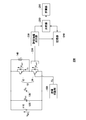
- FIG. 1 shows a configuration example of an evaluation circuit 100 that evaluates switching characteristics of a semiconductor device 10.
- An example of the result of measuring the switching characteristics of the semiconductor device 10 using the evaluation circuit 100 is shown.
- the structural example of the evaluation apparatus 200 in this embodiment is shown with the semiconductor device 10 to be evaluated.
- movement flow of the evaluation apparatus 200 which concerns on this embodiment is shown.
- An example of the evaluation index output by the evaluation index output unit 230 according to the present embodiment is shown.
- An example of the evaluation index output by the evaluation index output unit 230 according to the present embodiment is shown.
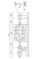
- the structural example which measures radiation noise of the motor drive device 600 carrying the semiconductor device 10 which concerns on this embodiment is shown.
- An example of the radiation noise measured by the measurement system shown in FIG. 6 is shown.
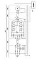
- FIG. 6 The structural example of the measurement system which measures the electric signal which drives the motor of the motor drive device 600 carrying the semiconductor device 10 which concerns on this embodiment is shown.
- An example of the voltage waveform measured by the measurement system shown in FIG. 8 is shown.
- An example of the voltage waveform measured by the measurement system shown in FIG. 8 is shown.
- the modification of the evaluation apparatus 200 which concerns on this embodiment is shown.
- An example in which the evaluation index output unit 230 according to the present embodiment outputs the turn-on characteristics of the semiconductor device 10 as an evaluation index is shown.
- An example in which the evaluation index output unit 230 according to the present embodiment outputs the turn-on characteristics of the semiconductor device 10 as an evaluation index is shown.
- the structural example of the composite evaluation apparatus 300 in this embodiment is shown with the database 410.
- movement flow of the composite evaluation apparatus 300 which concerns on this embodiment is shown.
- the composite evaluation apparatus 300 according to the present embodiment shows an example of a result of composite evaluation of radiation noise by combining a plurality of evaluation indexes shown in FIGS. 11A and 11B.
- the composite evaluation apparatus 300 according to the present embodiment shows an example of a result of composite evaluation of radiation noise by combining a plurality of evaluation indexes shown in FIGS. 11A and 11B.
- An example of a current waveform output from the semiconductor device 10 to be evaluated according to the present embodiment is shown.
- FIG. 1 shows a configuration example of an evaluation circuit 100 that evaluates the switching characteristics of the semiconductor device 10.
- the semiconductor device 10 to be evaluated shows an example including a first device 12 and a second device 14 connected in series.
- FIG. 1 shows an example in which the first device 12 is a diode and the second device 14 is a combination of diodes connected in reverse parallel to the IGBT.
- the evaluation circuit 100 includes a power source 110, a first capacitor unit 120, a second capacitor unit 130, a load reactor 140, and a signal supply unit 150.
- the power source 110 is a DC power source that outputs a DC voltage VDC .
- the power source 110 is connected to both ends of the semiconductor device 10.
- the power source 110 is connected to one end (cathode terminal) of the first device 12 and the other end (emitter terminal) of the second device 14, and supplies a DC voltage to the first device 12 and the second device 14.
- the other end (anode terminal) of the first device 12 is connected to one end (collector terminal) of the second device 14.
- the first capacitor unit 120 is connected in parallel with the semiconductor device 10 and smoothes the DC voltage VDC output from the power supply 110.
- the first capacitor 120 is, for example, a capacitor having a capacitance CDC .
- capacitance part 120 is an electrolytic capacitor as an example.
- the second capacitor unit 130 is connected in parallel with the semiconductor device 10 and suppresses a surge voltage.
- the second capacitive portion 130 is, for example, a capacitor of capacitance C S.
- the first capacitor unit 120 and the second capacitor unit 130 are desirably capacitors having different capacities. For example, the capacitor C DC is larger than the capacitor C S.
- the load reactor 140 is connected to both ends of the first device 12.
- the load reactor 140 has an inductance L as an example.
- the signal supply unit 150 supplies a predetermined switching signal to the semiconductor device 10.
- the signal supply unit 150 includes, for example, a pulse generator, an amplifier circuit, and the like, and supplies a pulsed switching signal V S to the gate terminal of the second device 14.
- the second device 14 switches the electrical connection state (ON state) and disconnection state (OFF state) between the collector terminal and the emitter terminal by supplying the switching signal V S to the gate terminal.
- the evaluation circuit 100 described above can switch the semiconductor device 10 by supplying a switching signal to the second device 14. Therefore, for example, the switching characteristics of the second device 14 can be acquired by measuring the collector current ic flowing through the collector terminal during the switching operation with an external measuring device or the like.
- the switching characteristic of the first device 12 can be evaluated by measuring the forward current if flowing in the first device 12 with an external measuring device or the like.
- the voltage between the collector and emitter terminals of the second device 14 is V ce2
- the voltage across the first device 12 is V r .
- FIG. 2 shows an example of the result of measuring the switching characteristics of the semiconductor device 10 using the evaluation circuit 100.
- the horizontal axis represents time
- the vertical axis represents voltage value or current value.
- FIG. 2 shows an example in which the evaluation circuit 100 switches the on state and the off state of the second device 14 by the switching signal V S so that the second device 14 is turned on and turned off.
- the switching signal V S becomes a high voltage at time t 1 and turns on the second device 14.
- a current flows from the power source 110 to the second device 14 via the load reactor 140.
- Current flowing to the second device 14 is observed as a collector current i c, increases substantially constant rate of change di / dt from the time t 1.
- the switching signal V S becomes a low voltage at time t 2 and turns off the second device 14.
- the evaluation circuit 100 when the collector current i c to a predetermined flow, to switch the second device 14 in an off state, may be set the time from time t 1 to time t 2. Thereby, the evaluation circuit 100 can execute the turn-off operation of the second device 14 under the condition of the collector current ic determined in advance. That is, it is possible to measure a transient response when the second device 14 is turned off under a predetermined collector current ic condition.
- the collector-emitter terminal voltage V ce2 is substantially the same voltage as the direct-current voltage V DC until the time t 1 when the second device 14 is in the off state.
- the voltage between the terminals V ce2 becomes substantially 0V.
- the first device 12 since the time until t 2 no current, forward current i f becomes substantially 0A.
- the voltage across V r of the first device 12 until the time t 1 is substantially 0V, the period from time t 1 to time t 2, the a DC voltage V DC and substantially the same voltage.
- the load reactor 140 works so as to continue the current that has been flowing, so that the current circulates from the load reactor 140 to the path of the first device 12. . Accordingly, forward current i f of the first device 12 rises at time t 2, the current value decreases gradually with time. Incidentally, the rise of the forward current i f at time t 2 of the first device 12, a forward recovery operation. Then, by turning on the second device 14 while the forward current if flows in the first device 12, the reverse recovery operation of the first device 12 and the turn-on operation of the second device 14 are performed. Can be executed.
- the evaluation circuit 100 when the predetermined forward current i f flows, to switch the second device 14 to the ON state may set the time from time t 2 to time t 3 . Thereby, the evaluation circuit 100 can execute the reverse recovery operation of the first device 12 and the turn-on operation of the second device 14 under the condition of a predetermined forward current if . That is, it is possible to measure the transient response of the second device 14 and the first device 12 when the second device 14 is turned on under a predetermined forward current if condition.
- the switching signal V S becomes the high voltage again at the time t 3 and turns on the second device 14.
- the inter-terminal voltage V ce2 of the second device 14 becomes substantially the same voltage as the direct-current voltage V DC during the time from the time t 2 to the time t 3 when the second device 14 is in the off state, and again becomes approximately 0 V from the time t 3. It becomes.
- the voltage V r across the first device 12 is substantially 0 V from time t 2 to time t 3 , and again becomes substantially the same voltage as the direct-current voltage V DC from time t 3 .
- the forward recovery operation of the first device 12 and the turn-off operation of the second device 14 can be observed at least partially in the same time domain with the same switching signal V S.
- the reverse recovery operation of the first device 12 and the turn-on operation of the second device 14 can be observed at least partially in the same time domain with the same switching signal V S.
- the signal supply unit 150 supplies a switching signal V S for turning on the second device 14 to the gate terminal of the second device 14.
- V S switching signal
- V ce2 of the second device 14 the turn-on characteristic of the second device 14 can be observed.
- the forward recovery characteristic of the first device 12 can be observed.
- the signal supply unit 150 supplies a switching signal V S for turning off the second device 14 to the gate terminal of the second device 14.
- V S switching signal
- the switching characteristics of the semiconductor device 10 are measured using the evaluation circuit 100, and for example, the semiconductor device 10 evaluated as a non-defective product that satisfies a predetermined standard is shipped to the market or the like.
- electromagnetic noise generated by the power conversion device may exceed a reference value defined by the EMC standard.
- EMC filter design, reselection of parts including the semiconductor device 10, substrate artwork, structural examination, etc. must be performed again, resulting in enormous labor and cost. End up.
- the evaluation apparatus 200 evaluates the switching characteristics of the semiconductor device 10 and evaluates the radiation noise of the semiconductor device 10 and outputs an evaluation index. Thereby, the radiation noise generated by the power conversion device or the like on which the semiconductor device 10 is mounted can be estimated before the power conversion device is completed, thereby reducing labor and cost in the manufacturing process. Such an evaluation apparatus 200 will be described next.
- FIG. 3 shows a configuration example of the evaluation apparatus 200 in the present embodiment, together with the semiconductor device 10 to be evaluated.
- a part of the evaluation device 200 has the same configuration as the evaluation circuit 100 shown in FIG. Therefore, by using the evaluation apparatus 200, the switching characteristics of the semiconductor device 10 described with reference to FIGS. 1 and 2 can be evaluated.
- the evaluation apparatus 200 includes a power source 110, a first capacitor unit 120, a second capacitor unit 130, a load reactor 140, a signal supply unit 150, a detection unit 220, an evaluation index output unit 230, and a storage unit 240.
- the comparison unit 250 and the evaluation unit 260 are provided.
- the power source 110, the first capacitor unit 120, the second capacitor unit 130, the load reactor 140, and the signal supply unit 150 illustrated in FIG. 3 are the same as the power source 110, the first capacitor unit 120, the second capacitor unit 130, which are described in FIG. Since the operations of the load reactor 140 and the signal supply unit 150 are substantially the same, the same reference numerals are given. Therefore, these descriptions are omitted here.
- FIG. 3 shows an example in which the semiconductor device 10 to be evaluated includes a first device 12 and a second device 14 connected in series.
- the first device 12 and the second device 14 are, for example, semiconductor switches such as MOSFETs or IGBTs.
- FIG. 3 shows an example in which the first device 12 and the second device 14 are IGBTs, and diodes are connected in antiparallel to each. That is, the load reactor 140 is connected between one end and the other end of the first device 12, and one end of the first device 12 is a collector terminal and the other end is an emitter terminal.
- the detection unit 220 detects a voltage change of the semiconductor device 10.
- the detection unit 220 detects, for example, voltage fluctuation of the semiconductor device 10 that changes according to the switching operation.
- the detection unit 220 observes a voltage change between the first device 12 and the second device 14.
- the detection unit 220 may include a collector-emitter terminal voltage V ce1 between one end and the other end of the first device 12 and a collector-emitter terminal voltage between the one end and the other end of the second device 14. It is good also as detecting the voltage between any one terminals of Vce2 .
- the detection unit 220 includes a voltage probe, and electrically connects the voltage probe to one end and the other end of the first device 12 and the second device 14.
- Evaluation index output unit 230 outputs an evaluation index of radiation noise of semiconductor device 10 based on the detection result of detection unit 220.
- the evaluation index output unit 230 outputs the frequency component of the voltage change detected by the detection unit 220 as the radiation noise evaluation index.
- the evaluation index output unit 230 includes a measuring device such as a spectrum analyzer that performs measurement in the frequency domain, and outputs a measurement result in the frequency domain as an evaluation index.
- the evaluation index output unit 230 includes a time domain measuring device such as an oscilloscope, performs Fourier transform on the time domain measurement result, converts it to frequency domain data, and outputs it as an evaluation index.
- the evaluation index output unit 230 supplies the evaluation index to the storage unit 240 and the comparison unit 250.
- the storage unit 240 stores the evaluation index output by the evaluation index output unit 230.
- the storage unit 240 stores an evaluation index in association with the evaluation target semiconductor device 10 evaluated by the evaluation apparatus 200.
- the storage unit 240 may store a past evaluation index that is evaluated and output by the evaluation apparatus 200, and may function as an evaluation index database.
- the storage unit 240 may be provided either inside or outside the evaluation apparatus 200.
- the storage unit 240 can also be a database connected to the main body of the evaluation apparatus 200 via a network or the like.
- the comparison unit 250 compares the evaluation index output this time by the evaluation index output unit 230 and a past evaluation index for a reference device different from the semiconductor device 10 stored in the storage unit 240.
- the comparison unit 250 compares the evaluation index of the reference device before improvement with the evaluation index of the semiconductor device 10 after improvement.
- the evaluation unit 260 evaluates the relative intensity change of the radiation noise of the semiconductor device 10 according to the comparison result of the comparison unit 250.
- the evaluation unit 260 outputs the evaluation result.
- the evaluation unit 260 may output the evaluation result to a display device or the like and further output the evaluation result to an external database or the like.
- the evaluation unit 260 may output the evaluation result in a predetermined format such as a data sheet.
- the evaluation apparatus 200 executes the switching operation of the semiconductor device 10 described with reference to FIGS. 1 and 2 and evaluates the radiation noise of the semiconductor device 10. Next, the evaluation operation of the semiconductor device 10 by the evaluation apparatus 200 will be described.
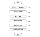
- FIG. 4 shows an operation flow of the evaluation apparatus 200 according to the present embodiment.
- the evaluation apparatus 200 performs the operations from S410 to S460 shown in FIG. 4 to evaluate the radiation noise of the semiconductor device 10 to be evaluated.
- the semiconductor device 10 to which the voltage probe of the detection unit 220 is electrically connected is caused to perform a switching operation (S410).
- a switching operation S410
- the signal supply section 150, a switching signal V S shown in Fig. 2 is supplied to the gate terminal of the second device 14, forward recovery operation and reverse recovery operation of the first device 12, and the turn-on operation of the second device 14 And switching operation such as turn-off operation.
- the detection unit 220 observes the voltage change of the semiconductor device 10 (S420).
- the detection unit 220 detects a voltage change between the collector terminal and the emitter terminal of the first device 12 and the second device 14 or a voltage change of one of the first device 12 and the second device 14.
- the frequency component of the voltage change is calculated (S430).
- the evaluation index output unit 230 frequency-converts the voltage change of the semiconductor device 10 detected by the detection unit 220, that is, the voltage waveform, and calculates the frequency component.
- the evaluation index output unit 230 may have a frequency domain measurement device such as a spectrum analyzer and observe a frequency component of a voltage change.
- a radiation noise evaluation index is output based on the voltage change (S440).
- the evaluation index output unit 230 outputs the calculated frequency characteristic of the voltage change as an evaluation index of radiation noise.
- the evaluation index is, for example, a calculation result of frequency characteristics in a predetermined frequency band such as 30 MHz to 1 GHz.
- the evaluation index output unit 230 outputs and stores the evaluation index in the storage unit 240. Further, the evaluation index output unit 230 supplies the evaluation index to the comparison unit 250. Further, the evaluation index output unit 230 may output the evaluation index as a part of the data sheet of the semiconductor device 10.
- the evaluation index output to the semiconductor device 10 is compared with the evaluation index output in the past to a reference device different from the semiconductor device 10 (S450).
- the comparison unit 250 reads a past evaluation index from the storage unit 240 and compares the evaluation index output by the evaluation index output unit 230 with the past evaluation index.
- the comparison unit 250 calculates a difference spectrum of the evaluation index in a predetermined frequency band.
- the evaluation unit 260 may use the difference spectrum as a relative intensity change. Further, the evaluation unit 260 may use a value corresponding to a predetermined frequency in the difference spectrum as a relative intensity change. Further, the evaluation unit 260 may use an average value of values corresponding to a plurality of predetermined frequencies as a relative intensity change in the difference spectrum.
- the evaluation unit 260 outputs a relative intensity change as an evaluation result.
- the evaluation unit 260 may output an evaluation result for each type of switching operation of the semiconductor device 10.
- the relative intensity change is an index of the relative radiation electric field intensity that is changed by mounting the semiconductor device 10 on the apparatus or the like.
- the relative intensity change is an indicator of device manufacturing variation or change over time, a difference in structure in which the device is mounted, and the like.
- the evaluation apparatus 200 can evaluate and output the radiation noise of the semiconductor device 10 by the above operation flow.
- the above evaluation apparatus 200 demonstrated the example which outputs the relative intensity
- the evaluation apparatus 200 may output an evaluation index indicating an absolute frequency spectrum calculated by the evaluation index output unit 230. Further, when the evaluation apparatus 200 is an apparatus that outputs an evaluation index, the comparison unit 250 and the evaluation unit 260 may be omitted.
- 5A and 5B show an example of an evaluation index output by the evaluation index output unit 230 according to the present embodiment.
- 5A and 5B show an example in which the evaluation index output unit 230 outputs the evaluation index of the semiconductor device 10 in the frequency band from 10 MHz to 500 MHz.
- the evaluation index output unit 230 includes the “forward recovery voltage” and the “reverse recovery voltage” of the first device 12 and the “turn-on voltage” of the second device 14 that are observed according to the predetermined switching signal V S. , And “turn-off voltage” frequency characteristics.
- FIG. 6 shows a configuration example of a measurement system for measuring radiation noise of the motor driving apparatus 600 equipped with the semiconductor device 10 according to the present embodiment.
- the motor drive device 600 is an example of a device on which the semiconductor device 10 is mounted.
- the motor drive device 600 includes a power supply unit 610, an input cable 620, a drive circuit 630, an output cable 640, and a motor 650.
- the power supply unit 610 is an AC power supply.
- the power supply unit 610 may include a power supply impedance stabilization circuit (LISN).
- the input cable 620 transmits the AC voltage output from the power supply unit 610 to the drive circuit 630.
- the drive circuit 630 generates an electrical signal that drives the motor 650.
- the drive circuit 630 rectifies the AC voltage of the power supply unit 610 by a rectifier circuit, and supplies the rectified signal to the inverter circuit to generate the electrical signal.
- the output cable 640 transmits an electrical signal output from the drive circuit 630 to the motor 650.
- the motor 650 rotates according to the electric signal.
- the semiconductor device 10 is mounted on the drive circuit 630 of such a motor drive device 600.
- the device S 1 in FIG. 6 is the first device 12, and the device S 4 is the second device 14.
- the device S 2 may be the first device 12 and the device S 5 may be the second device 14.
- the device S 3 may be the first device 12 and the device S 6 may be the second device 14.
- the semiconductor device 10 may be mounted as a part of the inverter circuit of the drive circuit 630. Since such a semiconductor device 10 performs a switching operation according to an electric signal, it generates radiation noise according to the operation.
- the antenna 660 and the measuring device 670 measure such radiation noise.
- the antenna 660 receives radiation noise that has propagated through space.
- the antenna 660 is disposed at a position separated from the motor driving device 600 by a predetermined distance.
- the measuring device 670 receives the received signal received by the antenna 660, converts the received signal into the frequency domain, and outputs the frequency domain.
- the measuring device 670 may measure a frequency region that is higher than the rotational frequency of the motor 650.
- the measuring device 670 may be a spectrum analyzer or the like.
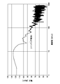
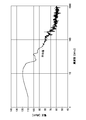
- FIG. 7A and 7B show an example of radiation noise measured by the measurement system shown in FIG. 7A and 7B show the radiation noise observed when the semiconductor device 10 is driven under two different conditions.
- the radiation electric field intensity in the frequency region from 30 MHz to 100 MHz is reduced by about 2 dB to 6 dB.
- FIG. 8 shows a configuration example of a measurement system for measuring an electric signal for driving a motor of the motor driving apparatus 600 equipped with the semiconductor device 10 according to the present embodiment.
- the same reference numerals are given to the substantially same operations as those of the measurement system shown in FIG.
- the motor drive device 600 is substantially the same device as that on which the semiconductor device 10 shown in FIG. 6 is mounted.
- the measuring device 670 measures an electrical signal that drives the motor 650 output from the drive circuit 630.
- the measuring device 670 measures the switching voltage waveform of the semiconductor device 10 while the motor 650 is being driven by the motor driving device 600.
- FIG. 9A and FIG. 9B show examples of voltage waveforms measured by the measurement system shown in FIG. FIG. 9A and FIG. 9B show the results of frequency analysis of the voltage waveform at the time of radiation noise measurement of FIG. 7A and FIG. 7B.
- the radiation electric field intensity in the frequency region from 30 MHz to 100 MHz tends to decrease by about 2 dB to 6 dB.
- the relative change values before and after the change of the driving condition A and the driving condition B show the same tendency in the frequency region from 30 MHz to 500 MHz, for example. Can be confirmed. That is, it can be seen that there is a correlation between the frequency component converted from the switching waveform of the semiconductor device 10 and the radiation noise, and the relative value of the radiation noise can be grasped based on the switching waveform of the semiconductor device 10. It can also be seen that by measuring such a correlation in advance, the radiation electric field strength of the radiation noise can be grasped based on the switching waveform of the semiconductor device 10.
- the evaluation apparatus 200 performs the turn-on operation, the turn-off operation, the reverse recovery operation, and the forward recovery operation of the semiconductor device 10 and evaluates the radiation noise based on the frequency characteristics of the obtained switching voltage waveform.
- the frequency characteristics of the switching voltage waveform obtained corresponding to the turn-on operation, turn-off operation, reverse recovery operation, and forward recovery operation are the turn-on characteristic, turn-off characteristic, reverse recovery characteristic, and forward recovery characteristic, respectively.
- the frequency characteristics of the switching voltage waveform obtained by the evaluation apparatus 200 can be obtained with different voltages depending on the switching operation.
- the reverse recovery characteristic may be a higher voltage than others. Therefore, it is desirable that the evaluation apparatus 200 executes a switching operation including at least the reverse recovery operation of the semiconductor device 10 and outputs an evaluation index.
- the evaluation apparatus 200 performs a switching operation including at least two operations among a turn-on operation, a turn-off operation, a reverse recovery operation, and a forward recovery operation of the semiconductor device, and outputs an evaluation index. In this case, it is more desirable that one of at least two operations is a reverse recovery operation.
- the turn-on characteristic may be the next higher voltage than the reverse recovery characteristic compared to the others. Therefore, it is more desirable that the evaluation apparatus 200 executes at least a switching operation including a reverse recovery operation and a turn-on operation of the semiconductor device 10 and outputs an evaluation index.
- the signal supply unit 150 may supply a switching signal for executing one or at least two operations among the turn-on operation, the turn-off operation, the reverse recovery operation, and the forward recovery operation of the semiconductor device 10. As a result, the evaluation apparatus 200 can shorten the evaluation time and can save time and effort for evaluation.
- the evaluation apparatus 200 has described an example in which a voltage change between the first device 12 and the second device 14 connected in series is observed.
- the evaluation apparatus 200 may observe voltage changes of the first device 12 and the second device 14. That is, the detection unit 220 is electrically connected to one end of the first device 12 and the other end of the second device 14, and detects a voltage change of the both-ends voltage of the first device 12 and the second device 14.
- Such a voltage across the first device 12 and the second device 14 has a waveform in which the high-frequency fluctuation component ⁇ V DC corresponding to the switching operation is superimposed on the DC voltage VDC supplied by the power supply 110.
- the evaluation apparatus 200 may evaluate the radiation noise of the semiconductor device 10 by observing the high-frequency fluctuation component ⁇ V DC .
- the semiconductor device 10 by the turn-on operation if the observed high-frequency fluctuation component [Delta] V DC, the voltage change turn-on characteristics of the reverse recovery characteristic and the second device 14 is superimposed in the first device 12 is observed. That is, in this case, the high-frequency fluctuation component ⁇ V DC has a correlation with the higher voltage among the reverse recovery characteristic of the first device 12 and the turn-on characteristic of the second device 14.
- the semiconductor device 10 by the turn-off operation if the observed high-frequency fluctuation component [Delta] V DC, the voltage change turn off characteristics of the forward recovery characteristic and the second device 14 is superimposed in the first device 12 is observed. That is, in this case, the high-frequency fluctuation component ⁇ V DC is correlated with the higher voltage characteristic of the forward recovery characteristic of the first device 12 and the turn-off characteristic of the second device 14.
- the evaluation apparatus 200 turns on and off the semiconductor device 10 and observes the high-frequency fluctuation component ⁇ V DC once, so that two of the four switching characteristics have a higher voltage. It can be observed. Further, since the measurement of the high frequency fluctuation component ⁇ V DC is an observation of the frequency characteristics excluding the DC component, it is easy to measure by AC coupling or insert a high pass filter between the detection unit 220 and the evaluation index output unit 230. ⁇ V DC component can be extracted. Therefore, the evaluation apparatus 200 can measure the high frequency fluctuation component ⁇ V DC by increasing the S / N and dynamic range.
- the evaluation apparatus 200 observes a voltage change of the semiconductor device 10 during the switching operation.
- the current flowing through the stray capacitance of the semiconductor device 10 may become a radiation noise source.
- a stray capacitance is formed between a part of the conductive member of the cooling fin and the semiconductor device 10, and a current flowing through the stray capacitance generates radiation noise.
- the evaluation apparatus 200 can execute the evaluation of relative radiation noise more accurately by acquiring the observation result in consideration of the noise generated by the stray capacitance. Such an evaluation apparatus 200 will be described next.
- FIG. 10 shows a modification of the evaluation apparatus 200 according to the present embodiment.
- the same reference numerals are given to substantially the same operations as those of the evaluation apparatus 200 according to the present embodiment shown in FIG. 3, and description thereof is omitted.
- the evaluation apparatus 200 according to the present modification further includes a conductive member 320 and a third capacitance unit 330.
- the conductive member 320 is a part of a temperature adjustment unit that adjusts the temperature of the semiconductor device 10.
- the conductive member 320 is a part of at least one of a heater, a cooling device, and a heat radiating fin.
- the conductive member 320 has a function of keeping the environmental temperature of the semiconductor device 10 stable. Therefore, it is desirable that the conductive member 320 is directly fixed to the semiconductor device 10. Thereby, the stray capacitance and the contact resistance between the semiconductor device 10 and the conductive member 320 can be maintained at a substantially constant and stable value.
- the evaluation apparatus 200 observes a voltage change with the semiconductor device 10 using the potential of the conductive member 320 fixed to the substrate on which the semiconductor device 10 is disposed as a reference potential.
- one of the voltage probes of the detection unit 220 is electrically connected to the conductive member 320 and the other is connected between the first device 12 and the second device 14, and the collector and emitter terminals of the second device 14 are connected.
- a change in the inter-voltage V ce2 is detected.
- the voltage probe of the detection unit 220 is electrically connected to one end on the collector terminal side of the first device 12 on one side and to the both ends of the first device 12 and the second device 14 on the other side. You may detect the voltage change of a voltage.
- the evaluation apparatus 200 of the present modification stabilizes the stray capacitance between the semiconductor device 10 and the conductive member 320.
- the conductive member 320 is used for temperature stabilization, it is desirable to increase the surface area and to make it larger than the stray capacitance of other paths. Further, such stray capacitance becomes a path through which a common mode current that causes radiation noise flows. Therefore, the evaluation apparatus 200 can output the evaluation index with higher reproducibility by stabilizing the noise generated by the stray capacitance and the common mode current.
- the evaluation apparatus 200 of the present modification includes a plurality of capacitor units connected in parallel to the semiconductor device, and at least one capacitor unit among the plurality of capacitor units is a plurality of capacitor elements connected in series. May be included.
- the evaluation apparatus 200 illustrated in FIG. 6 illustrates an example in which the third capacitor unit 330 includes a first capacitor element 332 and a second capacitor element 334.
- the first capacitor 332 and the second capacitor 334 are connected to the reference potential 340.
- the third capacitor unit 330 is a known circuit used as an EMC filter that reduces radiation noise. By providing such a circuit, the evaluation apparatus 200 can be brought closer to a circuit configuration in which the semiconductor device 10 is actually mounted, and output an evaluation result with higher accuracy.
- the evaluation device 200 may further include the same type and / or different types of EMC filters in addition to the third capacitance unit 330.
- the evaluation apparatus 200 can evaluate the radiation noise of the semiconductor device 10 by switching the semiconductor device 10.
- the switching current of the semiconductor device 10 may change from moment to moment. Since the radiation noise changes according to such a switching current, the result may be different from the evaluation index output by the evaluation apparatus 200.
- FIG. 11A and 11B show an example in which the evaluation index output unit 230 according to the present embodiment outputs the turn-on characteristics of the semiconductor device 10 as an evaluation index.
- the evaluation index is a turn-on characteristic when the switching current flowing through the semiconductor device 10 is changed according to the plurality of switching signals V S.
- FIG. 11A and FIG. 11B show the comparison target turn-on characteristics when the switching current is 0 A and three current switching currents corresponding to the predetermined current values I 1 , 2I 1 , and 3I 1. Two turn-on characteristics.
- the voltage changes nonlinearly depending on the switching current value.
- the current conditions for the maximum value are different at different frequencies.
- the current condition with a switching current of 3I 1 has a maximum value
- the current condition with a switching current of I 1 has a maximum value. Therefore, when the switching current of the semiconductor device 10 changes, the radiation noise generated according to the switching current can be estimated by combining a plurality of evaluation objects according to the change of the driving current.
- a composite evaluation apparatus 300 will be described next.
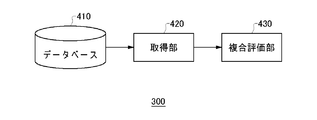
- FIG. 12 shows a configuration example of the composite evaluation apparatus 300 in the present embodiment, together with the database 410.
- the database 410 stores evaluation indexes output from the evaluation apparatus 200. It is desirable that the database 410 stores evaluation indexes that are output under a plurality of different switching signal conditions in a plurality of different switching operations of the semiconductor device 10. Note that the database 410 may be the storage unit 240 of the evaluation apparatus 200.
- the composite evaluation apparatus 300 performs composite evaluation of radiation noise emitted by the apparatus including the semiconductor device 10 using such an evaluation index.
- the apparatus on which the semiconductor device 10 as shown in FIG. 6 is mounted is called a mounting apparatus.
- the composite evaluation device 300 includes an acquisition unit 420 and a composite evaluation unit 430.
- the acquisition unit 420 acquires a plurality of evaluation indexes of the semiconductor device 10 output by the evaluation apparatus 200 in response to switching signals under a plurality of different conditions.
- the acquisition unit 420 acquires an evaluation index from the database 410 via, for example, a network. Further, the acquisition unit 420 may be directly connected to the database 410 and acquire an evaluation index.
- the acquisition unit 420 may also acquire information on drive signals that drive the semiconductor device 10.
- the composite evaluation unit 430 performs composite evaluation of the radiation noise of the mounting apparatus by combining a plurality of evaluation indexes according to the drive signal that drives the semiconductor device 10. For example, the composite evaluation unit 430 adds the voltages corresponding to the frequencies of the plurality of evaluation indexes for each predetermined frequency, and calculates the evaluation result of the radiation noise. Further, the composite evaluation unit 430 may calculate the average value or the maximum value of the voltage corresponding to the frequency of the plurality of evaluation indexes for each predetermined frequency, and calculate the evaluation result of the radiation noise. The composite evaluation unit 430 outputs the calculated evaluation result.
- FIG. 13 shows an operation flow of the composite evaluation apparatus 300 according to the present embodiment.
- the composite evaluation apparatus 300 performs the operations from S510 to S530 shown in FIG. 13 to compositely evaluate the radiation noise emitted from the semiconductor device 10 in the mounting apparatus.
- a drive signal for driving the semiconductor device 10 is acquired (S510).
- the acquisition unit 420 acquires information on a drive signal for driving the semiconductor device 10 by the mounting apparatus from the database 410 or the like. Instead of this, the acquisition unit 420 may be connected to the mounting apparatus and acquire information on the drive signal from the mounting apparatus. Instead, the information of the drive signal may be input to the acquisition unit 420 by a user of the composite evaluation apparatus 300 such as a designer or user of the mounting apparatus.
- the evaluation apparatus 200 acquires a plurality of evaluation indexes of the semiconductor device 10 output corresponding to the switching operations under a plurality of different conditions (S520).
- the acquisition unit 420 acquires a combination of a plurality of evaluation indexes corresponding to the drive signal of the semiconductor device 10.
- the acquisition unit 420 acquires a corresponding evaluation index according to, for example, the polarity and magnitude of the drive signal. Further, the acquisition unit 420 may acquire a corresponding evaluation index according to a temporal change in the drive signal.
- the acquisition unit 420 may calculate a plurality of evaluation indexes by multiplying the evaluation index by a weight corresponding to a temporal change in the drive signal.
- the composite evaluation unit 430 performs composite evaluation of the radiation noise of the mounting device by combining the plurality of evaluation indexes acquired by the acquisition unit 420 according to the drive signal for driving the semiconductor device 10 (S530).
- the combination of evaluation indexes used by the composite evaluation unit 430 is, for example, the maximum value or the sum of the plurality of evaluation indexes of the semiconductor device 10.
- the combination of evaluation indexes used by the composite evaluation unit 430 may be an average value of a plurality of evaluation indexes of the semiconductor device 10.
- the combination of evaluation indexes used by the composite evaluation unit 430 may be a maximum value or a sum of a plurality of evaluation indexes and an average value.
- the standard of radiation noise of electronic equipment by the International Committee on Radio Interference (CISPR) etc. is defined by quasi-peak value and average value. Therefore, in order to correspond to such a standard value, the composite evaluation unit 430 may perform composite evaluation of radiation noise using the maximum value and the average value of a plurality of evaluation indexes and output the result.
- the quasi-peak value can be predicted to some extent from the magnitude relationship of the difference between the output maximum value and average value.
- the combination of evaluation indexes used by the composite evaluation unit 430 is calculated after multiplying a plurality of weights corresponding to the current output from the semiconductor device 10 by the corresponding evaluation indexes among the plurality of evaluation indexes of the semiconductor device 10. It may be an average value.
- the composite evaluation apparatus 300 calculates an estimated value of radiation noise by combining evaluation indexes evaluated in advance with high accuracy in accordance with a drive signal for driving the semiconductor device 10, and thus performs composite evaluation of radiation noise. be able to.
- the composite evaluation apparatus 300 according to the present embodiment has an output current when the semiconductor device 10 is incorporated into the apparatus among a plurality of evaluation indexes evaluated by observing voltage changes of the semiconductor device 10 due to switching operations under various conditions. And obtain evaluation indices corresponding to switching current and combine them.
- the composite evaluation apparatus 300 can estimate more accurate radiation noise.
- FIG. 14A and FIG. 14B show an example of a result of the composite evaluation apparatus 300 according to the present embodiment performing composite evaluation of radiation noise by combining a plurality of evaluation indexes shown in FIG. 11A and FIG. 11B.
- FIG. 14A and FIG. 14B are examples of results obtained by the composite evaluation unit 430 adopting and outputting the maximum value and average value of a plurality of evaluation indexes as combinations. That is, in FIG. 14A, the waveform indicated as “maximum value” indicates the maximum value for each frequency of the four turn-on characteristics shown in FIGS. 11A and 11B. In FIG. 14B, a waveform indicated as “average value” indicates an average value for each frequency of the four turn-on characteristics shown in FIGS. 11A and 11B.
- the tendency of the quasi-peak value can be further predicted. For example, in the frequency region from 30 MHz to 60 MHz, it can be seen that the difference in voltage for each frequency of the two waveforms indicated by the average value and the maximum value is 6 dB or less. In this way, since the peak value and average value of radiation noise in the frequency domain are approximately the same level of intensity, the quasi-peak value of the frequency domain is at a high intensity level comparable to the peak value. Can be expected.
- the voltage difference between the frequencies of the two waveforms indicated by the average value and the maximum value is about 6 dB to 10 dB.
- the difference between the peak value and the average value of the radiation noise in the frequency domain is large, it can be expected that the quasi-peak value in the frequency domain has a low intensity level equivalent to the average value.
- the composite evaluation apparatus 300 can combine the plurality of evaluation indexes to perform composite evaluation of radiation noise, and thus can predict the radiation noise level of the regulated device based on the composite evaluation result.
- the composite evaluation apparatus 300 can also perform composite evaluation of radiation noise corresponding to more complicated drive signals.
- FIG. 15 shows an example in which the output current waveform in a half cycle for one phase is normalized when the device is, for example, a three-phase inverter device.
- the horizontal axis represents a normalized time axis
- the vertical axis represents the normalized amplitude value of the drive signal. Since the output current is a part of the sine wave signal, the horizontal axis, which is the time axis in FIG.
- the acquisition unit 420 acquires, as an example, an evaluation index that is output according to the turn-on operation of the semiconductor device 10.
- the acquisition unit 420 may acquire the evaluation index output by the evaluation device 200 under conditions corresponding to the peak value of the amplitude of the sine wave.
- the acquisition unit 420 may acquire the evaluation index output by the evaluation device 200 under a condition closest to the peak value of the amplitude value of the sine wave. For example, the acquisition unit 420 multiplies the evaluation index acquired by the weight according to the output current to acquire a plurality of evaluation indexes.
- the acquisition unit 420 divides the output current into a plurality of regions according to the amplitude value.
- FIG. 15 shows four regions of 0 to 0.25, 0, 25 to 0.5, 0, 5 to 0.75, and 0.75 to 1 when the amplitude of the output current is set to 1. Shows an example of equal division.
- the acquisition unit 420 calculates the time axis occupancy of the drive signal in each region. For example, in the region where the amplitude intensity is 0 to 0.25, the output current is occupied at the first rising edge and the last falling edge of the time axis. That is, the region having the amplitude intensity from 0 to 0.25 occupies 16% of the phase region with respect to the entire phase region where the output current is 100%, so the occupation ratio is set to 16%.
- the acquisition unit 420 has an occupancy rate of 17% for an area with an amplitude intensity of 0.25 to 0.5, an occupancy ratio of 21% for an area with an amplitude intensity of 0.5 to 0.75, and an amplitude intensity of 0.
- the occupation ratio of the region from 75 to 1 is assumed to be 46%. Since the distribution of the occupancy rate can be directly replaced with the occurrence frequency of the switching current in the three-phase inverter operation, the acquisition unit 420 can calculate a plurality of evaluation indexes according to the occupancy rate.
- the acquisition unit 420 multiplies the voltage for each frequency of the reference evaluation index acquired in accordance with the peak value of the amplitude value of the output current by 0.16, so that the amplitude intensity ranges from 0 to 0.25.
- the first evaluation index is calculated.
- the acquisition unit 420 calculates the second evaluation index in the region where the amplitude intensity is 0.25 to 0.5 by multiplying the reference evaluation index by 0.17.
- the acquisition unit 420 multiplies the reference evaluation index by 0.21 and 0.46, respectively, so that the third evaluation index and the amplitude intensity in the region where the amplitude intensity is 0.5 to 0.75 are 0.
- the composite evaluation unit 430 calculates an average value for each frequency of the four evaluation indices from the first evaluation index to the fourth evaluation index as a composite evaluation value of radiation noise.
- the composite evaluation unit 430 outputs the calculated composite evaluation value.
- the composite evaluation apparatus 300 uses a plurality of evaluation indexes that consider the frequency of occurrence of the switching current according to the output current, and therefore radiates more accurately in response to various output currents. Noise can be evaluated in combination.
- the example in which the amplitude of the output current is equally divided into four regions has been described.
- the present invention is not limited to this.
- the number of divisions of the amplitude of the drive signal may be set to various division numbers.
- the weight or the like multiplied by the evaluation index may be adjustable according to the drive signal.
- the evaluation apparatus 200 and the composite evaluation apparatus 300 can evaluate the radiation noise when the semiconductor device 10 is mounted on the apparatus before the semiconductor device 10 is mounted on the apparatus or the like. it can. Even if the drive signal for driving the semiconductor device 10 is complicated, the composite evaluation apparatus 300 can perform composite evaluation of radiation noise by combining evaluation indexes output from the evaluation apparatus 200.
- the evaluation apparatus 200 by outputting the evaluation index output from the evaluation apparatus 200 as the data sheet of the semiconductor device 10, it is possible to provide meaningful information that facilitates the apparatus design. In this case, it is desirable that the evaluation apparatus 200 outputs an evaluation index together with an evaluation result for a past device. Thereby, for example, it is possible to easily grasp how much the radiation noise is reduced or increased from the devices used in the past, and the apparatus design can be executed smoothly.
- the driving condition includes a relationship between a gate voltage value input to the gate terminal of the semiconductor device and time.
- the drive circuit constant includes a gate resistance value, an inductance value of the gate wiring, a capacity, a specification of a power source to be used, and the like. Further, for example, when the radiation noise generated when the semiconductor device is turned on in the lower arm of the half bridge circuit is dominant, the driving condition or driving circuit constant of the semiconductor device in the lower arm is adjusted.
- a shield plate is provided between the printed circuit board and the semiconductor device where radiation noise is dominant. Or grounding to the ground.
- the internal resistance value of the device may be adjusted.
- the shape of the housing (case) used for the module such as adjustment of thickness / material, shape / size / material of wiring (wire, lead frame, etc.) bonded on the surface electrode formed on the semiconductor device, etc. Material adjustment and the like may be performed.
- the evaluation apparatus 200 and the composite evaluation apparatus 300 have been described as separate independent apparatuses, but the present invention is not limited to such a configuration.
- the evaluation apparatus 200 and the composite evaluation apparatus 300 may be configured as one apparatus, for example.
- at least a part of the evaluation apparatus 200 and / or the composite evaluation apparatus 300 may be configured by a computer or the like.
- the dedicated circuit may include a digital and / or analog hardware circuit, and may include an integrated circuit (IC) and / or a discrete circuit.
- Programmable circuits include logical sums, exclusive logical sums, negative logical products, negative logical sums, and other logical operations such as field programmable gate arrays (FPGAs) and programmable logic arrays (PLA), flip-flops, etc. , Registers, and memory elements, including reconfigurable hardware circuitry.
- a computer-readable storage medium may include any tangible device capable of storing instructions to be executed by a suitable device.
- a computer readable storage medium having instructions stored on the tangible device comprises a product including instructions that can be executed to create a means for performing the operations specified in the flowchart or block diagram. become.
- Examples of computer readable storage media may include electronic storage media, magnetic storage media, optical storage media, electromagnetic storage media, semiconductor storage media, and the like.
- Computer-readable storage media include floppy disks, diskettes, hard disks, random access memory (RAM), read only memory (ROM), erasable programmable read only memory (EPROM or flash memory). Electrically erasable programmable read only memory (EEPROM), static random access memory (SRAM), compact disc read only memory (CD-ROM), digital versatile disc (DVD), Blu-ray (registered trademark) disc, memory stick Integrated circuit cards and the like may be included.
- RAM random access memory
- ROM read only memory
- EPROM or flash memory erasable programmable read only memory
- EEPROM Electrically erasable programmable read only memory
- SRAM static random access memory
- CD-ROM compact disc read only memory
- DVD digital versatile disc
- Blu-ray registered trademark
- Computer readable instructions may include assembler instructions, instruction set architecture (ISA) instructions, machine instructions, machine dependent instructions, microcode, firmware instructions, state setting data, and the like.
- Computer-readable instructions also include object-oriented programming languages such as Smalltalk, JAVA, C ++, etc., and conventional procedural programming languages such as the “C” programming language or similar programming languages, or It may include source code or object code written in any combination of multiple programming languages.
- the computer readable instructions may be a general purpose computer, special purpose computer, or processor of other programmable data processing device, locally or via a wide area network (WAN) such as a local area network (LAN), the Internet, etc. Or it may be provided in a programmable circuit.
- WAN wide area network
- LAN local area network
- Computer readable instructions can be executed.
- the processor include a computer processor, a processing unit, a microprocessor, a digital signal processor, a controller, a microcontroller, and the like.
Landscapes
- Physics & Mathematics (AREA)
- General Physics & Mathematics (AREA)
- Electromagnetism (AREA)
- Engineering & Computer Science (AREA)
- Microelectronics & Electronic Packaging (AREA)
- Testing Of Individual Semiconductor Devices (AREA)
Abstract
半導体デバイスの放射ノイズを簡便に評価し、半導体デバイスが搭載された装置の放射ノイズを推定する。 半導体デバイスにスイッチング動作させる段階と、スイッチング動作中の半導体デバイスの主端子間に生じる電圧変化を測定する段階と、電圧変化に基づき、半導体デバイスの放射ノイズの評価指標を出力する段階とを備える、評価方法および評価装置を提供する。評価指標を出力する段階は、評価指標として、半導体デバイスの電圧変化を周波数成分ごとに算出してよい。
Description
本発明は、評価方法、推定方法、評価装置、および複合評価装置に関する。
従来、インバータおよびPWM整流器等の電力変換装置をはじめとする電気電子機器が発生する電磁ノイズ(伝導・放射)には、EMC(Electro-Magnetic Compatibility)規格によって限度値が定められており、十分に電磁ノイズを低減することが求められている。このような電力変換装置の動作時に発生する電磁ノイズを、シミュレーションまたは簡易的な測定によって評価する方法が提案されていた(例えば、特許文献1から3参照)。
特許文献1 特開平6-309420号
特許文献2 特開2014-135095号
特許文献3 特開2005-233833号
特許文献1 特開平6-309420号
特許文献2 特開2014-135095号
特許文献3 特開2005-233833号
このようなシミュレーションは、解析モデルを用いる。しかしながら、当該解析モデルは、電力変換装置の回路基板や筐体構造の詳細が決まった後でなければ作成できない。また、簡易な測定による電磁ノイズ評価も、電力変換装置が完成した後でなければ評価することができない。したがって、電力変換装置が完成した後に電磁ノイズの評価結果が「規格不適合」となることもあり、この場合、EMCフィルタ設計、部品選定、基板アートワーク、および構造検討等を再度実施しなければならなかった。
(項目1)
評価方法は、半導体デバイスにスイッチング動作させる段階を備えてよい。
評価方法は、スイッチング動作中の半導体デバイスの主端子間に生じる電圧変化を測定する段階を備えてよい。
評価方法は、電圧変化に基づき、半導体デバイスの放射ノイズの評価指標を出力する段階を備えてよい。
(項目2)
評価指標を出力する段階は、評価指標として、半導体デバイスの電圧変化を周波数成分ごとに算出してよい。
(項目3)
スイッチング動作は、半導体デバイスのターンオン動作、ターンオフ動作、逆回復動作、および順回復動作のうち、少なくとも2つの動作を含んでよい。
(項目4)
半導体デバイスは、直列に接続された第1デバイスおよび第2デバイスを含んでよい。
測定する段階は、第1デバイスおよび第2デバイスの間の電圧変化を測定してよい。
(項目5)
半導体デバイスは、直列に接続された第1デバイスおよび第2デバイスを含んでよい。
測定する段階は、第1デバイスおよび第2デバイスの電圧変化を測定してよい。
(項目6)
測定する段階は、半導体デバイスが絶縁材を介して取り付けられた導電性部材の電位を基準電位として、半導体デバイスとの間の電圧変化を測定してよい。
(項目7)
評価方法は、半導体デバイスに対して出力した評価指標と、半導体デバイスとは異なる基準デバイスに対して出力した評価指標と、を比較する段階を備えてよい。
評価方法は、比較結果に応じて、基準デバイスに対する半導体デバイスの放射ノイズの強度を評価する段階を備えてよい。
(項目8)
推定方法は、半導体デバイスを備える装置の放射ノイズを推定してよい。
推定方法は、項目1から7のいずれか一項に記載の評価方法によって、複数の条件におけるスイッチング動作に対応して出力された半導体デバイスの複数の評価指標を取得する段階を備えてよい。
推定方法は、複数の評価指標を組み合わせて装置の放射ノイズを推定する段階を備えてよい。
(項目9)
評価指標の組み合わせは、半導体デバイスの複数の評価指標の最大値または和でよい。
(項目10)
評価指標の組み合わせは、半導体デバイスの複数の評価指標の平均値でよい。
(項目11)
評価指標の組み合わせは、複数の条件に対するそれぞれの重みを、半導体デバイスの複数の評価指標のうち対応する評価指標にそれぞれ乗じてから算出する平均値でよい。
評価方法は、半導体デバイスにスイッチング動作させる段階を備えてよい。
評価方法は、スイッチング動作中の半導体デバイスの主端子間に生じる電圧変化を測定する段階を備えてよい。
評価方法は、電圧変化に基づき、半導体デバイスの放射ノイズの評価指標を出力する段階を備えてよい。
(項目2)
評価指標を出力する段階は、評価指標として、半導体デバイスの電圧変化を周波数成分ごとに算出してよい。
(項目3)
スイッチング動作は、半導体デバイスのターンオン動作、ターンオフ動作、逆回復動作、および順回復動作のうち、少なくとも2つの動作を含んでよい。
(項目4)
半導体デバイスは、直列に接続された第1デバイスおよび第2デバイスを含んでよい。
測定する段階は、第1デバイスおよび第2デバイスの間の電圧変化を測定してよい。
(項目5)
半導体デバイスは、直列に接続された第1デバイスおよび第2デバイスを含んでよい。
測定する段階は、第1デバイスおよび第2デバイスの電圧変化を測定してよい。
(項目6)
測定する段階は、半導体デバイスが絶縁材を介して取り付けられた導電性部材の電位を基準電位として、半導体デバイスとの間の電圧変化を測定してよい。
(項目7)
評価方法は、半導体デバイスに対して出力した評価指標と、半導体デバイスとは異なる基準デバイスに対して出力した評価指標と、を比較する段階を備えてよい。
評価方法は、比較結果に応じて、基準デバイスに対する半導体デバイスの放射ノイズの強度を評価する段階を備えてよい。
(項目8)
推定方法は、半導体デバイスを備える装置の放射ノイズを推定してよい。
推定方法は、項目1から7のいずれか一項に記載の評価方法によって、複数の条件におけるスイッチング動作に対応して出力された半導体デバイスの複数の評価指標を取得する段階を備えてよい。
推定方法は、複数の評価指標を組み合わせて装置の放射ノイズを推定する段階を備えてよい。
(項目9)
評価指標の組み合わせは、半導体デバイスの複数の評価指標の最大値または和でよい。
(項目10)
評価指標の組み合わせは、半導体デバイスの複数の評価指標の平均値でよい。
(項目11)
評価指標の組み合わせは、複数の条件に対するそれぞれの重みを、半導体デバイスの複数の評価指標のうち対応する評価指標にそれぞれ乗じてから算出する平均値でよい。
(項目12)
評価装置は、評価対象の半導体デバイスに予め定められたスイッチング信号を供給する信号供給部を備えてよい。
評価装置は、半導体デバイスの電圧変化を検出する検出部を備えてよい。
評価装置は、検出部の検出結果に基づき、半導体デバイスの放射ノイズの評価指標を出力する評価指標出力部を備えてよい。
(項目13)
評価指標出力部は、電圧変化の周波数成分に基づき、半導体デバイスの放射ノイズに対応する電界強度を算出してよい。
(項目14)
信号供給部は、半導体デバイスのターンオン動作、ターンオフ動作、逆回復動作、および順回復動作のうち、少なくとも2つの動作を実行させるスイッチング信号を供給してよい。
(項目15)
半導体デバイスは、直列に接続された第1デバイスおよび第2デバイスを含んでよい。
検出部は、第1デバイスおよび第2デバイスの間の電圧変化を測定してよい。
(項目16)
半導体デバイスは、直列に接続された第1デバイスおよび第2デバイスを含んでよい。
検出部は、第1デバイスおよび第2デバイスの主端子間に生じる電圧変化を測定してよい。
(項目17)
評価装置は、評価指標出力部が出力する評価指標を記憶する記憶部を備えてよい。
評価装置は、評価指標出力部が出力した評価指標と、記憶部に記憶された半導体デバイスとは異なる基準デバイスに対する評価指標と、を比較する比較部を備えてよい。
評価装置は、比較結果に応じて、半導体デバイスの放射ノイズの評価指標の相対的な強度変化を評価する評価部を備えてよい。
(項目18)
検出部は、半導体デバイスが絶縁材を介して取り付けられた導電性部材の電位を基準電位として、半導体デバイスとの間の電圧変化を測定してよい。
(項目19)
複合評価装置は、項目12から18のいずれか一項に記載の評価装置によって、複数の条件におけるスイッチング信号に対応して出力された半導体デバイスの複数の評価指標を取得する取得部を備えてよい。
複合評価装置は、複数の評価指標を組み合わせて半導体デバイスを備える装置の放射ノイズを推定する複合評価部を備えてよい。
評価装置は、評価対象の半導体デバイスに予め定められたスイッチング信号を供給する信号供給部を備えてよい。
評価装置は、半導体デバイスの電圧変化を検出する検出部を備えてよい。
評価装置は、検出部の検出結果に基づき、半導体デバイスの放射ノイズの評価指標を出力する評価指標出力部を備えてよい。
(項目13)
評価指標出力部は、電圧変化の周波数成分に基づき、半導体デバイスの放射ノイズに対応する電界強度を算出してよい。
(項目14)
信号供給部は、半導体デバイスのターンオン動作、ターンオフ動作、逆回復動作、および順回復動作のうち、少なくとも2つの動作を実行させるスイッチング信号を供給してよい。
(項目15)
半導体デバイスは、直列に接続された第1デバイスおよび第2デバイスを含んでよい。
検出部は、第1デバイスおよび第2デバイスの間の電圧変化を測定してよい。
(項目16)
半導体デバイスは、直列に接続された第1デバイスおよび第2デバイスを含んでよい。
検出部は、第1デバイスおよび第2デバイスの主端子間に生じる電圧変化を測定してよい。
(項目17)
評価装置は、評価指標出力部が出力する評価指標を記憶する記憶部を備えてよい。
評価装置は、評価指標出力部が出力した評価指標と、記憶部に記憶された半導体デバイスとは異なる基準デバイスに対する評価指標と、を比較する比較部を備えてよい。
評価装置は、比較結果に応じて、半導体デバイスの放射ノイズの評価指標の相対的な強度変化を評価する評価部を備えてよい。
(項目18)
検出部は、半導体デバイスが絶縁材を介して取り付けられた導電性部材の電位を基準電位として、半導体デバイスとの間の電圧変化を測定してよい。
(項目19)
複合評価装置は、項目12から18のいずれか一項に記載の評価装置によって、複数の条件におけるスイッチング信号に対応して出力された半導体デバイスの複数の評価指標を取得する取得部を備えてよい。
複合評価装置は、複数の評価指標を組み合わせて半導体デバイスを備える装置の放射ノイズを推定する複合評価部を備えてよい。
なお、上記の発明の概要は、本発明の必要な特徴の全てを列挙したものではない。また、これらの特徴群のサブコンビネーションもまた、発明となりうる。
以下、発明の実施の形態を通じて本発明を説明するが、以下の実施形態は請求の範囲にかかる発明を限定するものではない。また、実施形態の中で説明されている特徴の組み合わせの全てが発明の解決手段に必須であるとは限らない。
図1は、半導体デバイス10のスイッチング特性を評価する評価回路100の構成例を示す。評価対象の半導体デバイス10は、直列に接続された第1デバイス12および第2デバイス14を含む例を示す。図1は、第1デバイス12がダイオードであり、第2デバイス14がIGBTと逆並列接続されたダイオードの組み合わせである例を示す。図1に示す評価回路100を用いて、第2デバイス14のターンオン動作およびターンオフ動作等を実行することにより、半導体デバイス10のスイッチング損失およびサージ電圧等を評価することができる。評価回路100は、電源110と、第1容量部120と、第2容量部130と、負荷リアクトル140と、信号供給部150と、を備える。
電源110は、直流電圧VDCを出力する直流電源である。電源110は、半導体デバイス10の両端に接続される。電源110は、例えば、第1デバイス12の一端(カソード端子)と第2デバイス14の他端(エミッタ端子)に接続され、第1デバイス12および第2デバイス14に直流電圧を供給する。この場合、第1デバイス12の他端(アノード端子)が第2デバイス14の一端(コレクタ端子)に接続される。
第1容量部120は、半導体デバイス10と並列に接続され、電源110から出力される直流電圧VDCを平滑化する。第1容量部120は、例えば、容量CDCのコンデンサである。第1容量部120は、一例として、電解コンデンサである。第2容量部130は、半導体デバイス10と並列に接続され、サージ電圧を抑制する。第2容量部130は、例えば、容量CSのコンデンサである。第1容量部120および第2容量部130は、異なる容量のコンデンサであることが望ましく、例えば、容量CDCは、容量CSよりも大きい容量である。
負荷リアクトル140は、第1デバイス12の両端に接続される。負荷リアクトル140は、一例として、インダクタンスLを有している。
信号供給部150は、半導体デバイス10に予め定められたスイッチング信号を供給する。信号供給部150は、例えば、パルス発生装置および増幅回路等を有し、第2デバイス14のゲート端子にパルス状のスイッチング信号VSを供給する。第2デバイス14は、当該スイッチング信号VSがゲート端子に供給されることにより、コレクタ端子およびエミッタ端子間の電気的な接続状態(オン状態)および切断状態(オフ状態)を切り換える。
以上の評価回路100は、スイッチング信号を第2デバイス14に供給して、半導体デバイス10をスイッチング動作させることができる。したがって、例えば、スイッチング動作中のコレクタ端子に流れるコレクタ電流icを外部の測定装置等で測定することで、第2デバイス14のスイッチング特性を取得することができる。
また、スイッチング動作中において、第1デバイス12に流れる順方向電流ifを外部の測定装置等で測定することで、第1デバイス12のスイッチング特性を評価することができる。なお、第2デバイス14のコレクタおよびエミッタの端子間電圧をVce2とし、第1デバイス12の両端電圧をVrとする。評価回路100を用いたスイッチング特性の測定について次に説明する。
図2は、評価回路100を用いて半導体デバイス10のスイッチング特性を測定した結果の一例を示す。図2は、横軸を時間、縦軸を電圧値または電流値とする。図2は、評価回路100がスイッチング信号VSにより、第2デバイス14のオン状態およびオフ状態を切り換えて、第2デバイス14にターンオン動作およびターンオフ動作させた例を示す。
スイッチング信号VSは、時刻t1においてハイ電圧となり、第2デバイス14をオン状態にする。第2デバイス14のコレクタ端子およびエミッタ端子の間が導通になることにより、電源110から負荷リアクトル140を介して第2デバイス14へと電流が流れる。第2デバイス14へと流れる電流は、コレクタ電流icとして観測され、時刻t1から略一定の変化率di/dtで上昇する。ここで、変化率di/dtは、次式で示される。
(数1)
di/dt=VDC/L
(数1)
di/dt=VDC/L
また、スイッチング信号VSは、時刻t2においてロー電圧となり、第2デバイス14をオフ状態にする。ここで、評価回路100は、予め定められたコレクタ電流icが流れた時点で、第2デバイス14をオフ状態に切り換えるように、時刻t1から時刻t2までの時間を設定してよい。これにより、評価回路100は、予め定められたコレクタ電流icの条件における、第2デバイス14のターンオフ動作を実行することができる。即ち、予め定められたコレクタ電流icの条件で第2デバイス14をターンオフ動作させた場合の、過渡応答を測定することができる。
なお、コレクタおよびエミッタの端子間電圧Vce2は、第2デバイス14がオフ状態の時刻t1までの時間において、直流電圧VDCと略同一の電圧となる。そして、時刻t1から時刻t2までの時間において、第2デバイス14がオン状態となるので、端子間電圧Vce2は略0Vとなる。また、第1デバイス12は、時刻t2までの時間は電流を流さないので、順方向電流ifは略0Aとなる。また、第1デバイス12の両端電圧Vrは、時刻t1までは略0Vであり、時刻t1から時刻t2までの時間において、直流電圧VDCと略同一の電圧となる。
時刻t2において、第2デバイス14がオフ状態になると、負荷リアクトル140は、流れていた電流を継続させて流すように働くので、当該負荷リアクトル140から第1デバイス12の経路に電流が環流する。したがって、第1デバイス12の順方向電流ifは、時刻t2において立ち上がり、時間と共に電流値が徐々に減少する。なお、第1デバイス12の時刻t2における順方向電流ifの立ち上がりを、順回復動作とする。そして、第1デバイス12に順方向電流ifが流れているうちに、第2デバイス14をオン状態とすることで、当該第1デバイス12の逆回復動作と、第2デバイス14のターンオン動作を実行することができる。
ここで、評価回路100は、予め定められた順方向電流ifが流れた時点で、第2デバイス14をオン状態に切り換えるように、時刻t2から時刻t3までの時間を設定してよい。これにより、評価回路100は、予め定められた順方向電流ifの条件における、第1デバイス12の逆回復動作および第2デバイス14のターンオン動作を実行することができる。即ち、予め定められた順方向電流ifの条件で第2デバイス14をターンオン動作させた場合の、第2デバイス14および第1デバイス12の過渡応答を測定することができる。
このように、スイッチング信号VSは、時刻t3において再びハイ電圧となり、第2デバイス14をオン状態にする。第2デバイス14の端子間電圧Vce2は、第2デバイス14がオフ状態の時刻t2から時刻t3までの時間において、直流電圧VDCと略同一の電圧となり、時刻t3から再び略0Vとなる。また、第1デバイス12の両端電圧Vrは、時刻t2から時刻t3までの時間において、略0Vとなり、時刻t3から再び直流電圧VDCと略同一の電圧となる。
なお、第1デバイス12の順回復動作および第2デバイス14のターンオフ動作は、同一のスイッチング信号VSで、少なくとも一部が同一の時間領域で観測できる。同様に、第1デバイス12の逆回復動作および第2デバイス14のターンオン動作も、同一のスイッチング信号VSで、少なくとも一部が同一の時間領域で観測できる。
例えば、信号供給部150が、第2デバイス14をターンオン動作させるスイッチング信号VSを第2デバイス14のゲート端子に供給した場合を考える。この場合において、第2デバイス14のコレクタ・エミッタの端子間電圧Vce2の過渡応答を検出すると、第2デバイス14のターンオン特性を観測することができる。また、第1デバイス12に流れる電流ifを検出すると、第1デバイス12の順回復特性を観測することができる。
同様に、信号供給部150が、第2デバイス14をターンオフ動作させるスイッチング信号VSを第2デバイス14のゲート端子に供給した場合を考える。この場合において、第2デバイス14のコレクタ・エミッタの端子間電圧Vce2を検出すると、第2デバイス14のターンオフ特性を観測することができる。また、第1デバイス12に流れる電流ifを検出すると、第1デバイス12の逆回復特性を観測することができる。
このように、評価回路100を用いて半導体デバイス10のスイッチング特性を測定し、例えば、予め定められた基準を満たす良品と評価された半導体デバイス10が、市場等に出荷される。しかしながら、スイッチング特性が良好な半導体デバイス10を用いて電力変換装置等を製造しても、当該電力変換装置が発生する電磁ノイズがEMC規格で定められた基準値を超えてしまうことがある。この場合、電力変換装置が完成した後に、EMCフィルタ設計、半導体デバイス10を含む部品の再選定、基板アートワーク、および構造検討等を再度実施しなければならず、膨大な手間とコストが発生してしまう。
そこで、本実施形態に係る評価装置200は、半導体デバイス10のスイッチング特性を評価すると共に、当該半導体デバイス10の放射ノイズを評価して評価指標を出力する。これにより、当該半導体デバイス10を搭載した電力変換装置等が発生する放射ノイズを、当該電力変換装置が完成する前に推定することができ、製造過程における手間とコストを低減させる。このような評価装置200について、次に説明する。
図3は、本実施形態における評価装置200の構成例を、評価対象の半導体デバイス10と共に示す。評価装置200は、一部が図1に示す評価回路100と同様の構成である。したがって、評価装置200を用いることで、図1および図2で説明した半導体デバイス10のスイッチング特性を評価することができる。評価装置200は、電源110と、第1容量部120と、第2容量部130と、負荷リアクトル140と、信号供給部150と、検出部220と、評価指標出力部230と、記憶部240と、比較部250と、評価部260と、を備える。
図3に示す電源110、第1容量部120、第2容量部130、負荷リアクトル140、および信号供給部150は、図1で説明した電源110、第1容量部120、第2容量部130、負荷リアクトル140、および信号供給部150の動作と略同一なので、同一の符号を付している。したがって、ここではこれらの説明を省略する。
なお、図3において、評価対象の半導体デバイス10は、直列に接続された第1デバイス12および第2デバイス14を含む例を示す。ここで、第1デバイス12および第2デバイス14は、例としてMOSFETまたはIGBT等の半導体スイッチである。図3は、第1デバイス12および第2デバイス14がIGBTで、それぞれにダイオードが逆並列に接続されている例を示す。即ち、負荷リアクトル140は、第1デバイス12の一端および他端の間に接続され、第1デバイス12の一端はコレクタ端子であり、他端はエミッタ端子である。
検出部220は、半導体デバイス10の電圧変化を検出する。検出部220は、例えば、スイッチング動作に応じて変化する半導体デバイス10の電圧変動を検出する。検出部220は、例えば、第1デバイス12および第2デバイス14の間の電圧変化を観測する。または、検出部220は、第1デバイス12の一端および他端の間の、コレクタ・エミッタの端子間電圧Vce1、第2デバイス14の一端および他端の間の、コレクタ・エミッタの端子間電圧Vce2のいずれか一方の端子間電圧を検出することとしてもよい。検出部220は、電圧プローブを有し、当該電圧プローブを第1デバイス12および第2デバイス14の一端および他端に、電気的に接続する。
評価指標出力部230は、検出部220の検出結果に基づき、半導体デバイス10の放射ノイズの評価指標を出力する。評価指標出力部230は、検出部220が検出した電圧変化の周波数成分を放射ノイズの評価指標として出力する。一例として、評価指標出力部230は、スペクトラムアナライザ等の周波数ドメインの測定を実行する測定器を有し、周波数ドメインの測定結果を評価指標として出力する。また、評価指標出力部230は、オシロスコープ等の時間ドメインの測定器を有し、時間ドメインの測定結果をフーリエ変換して、周波数ドメインのデータに変換し、評価指標として出力する。評価指標出力部230は、評価指標を記憶部240および比較部250に供給する。
記憶部240は、評価指標出力部230が出力する評価指標を記憶する。記憶部240は、例えば、当該評価装置200が評価した評価対象の半導体デバイス10と対応付けて、評価指標を記憶する。記憶部240は、一例として、当該評価装置200が評価して出力した過去の評価指標を記憶して、評価指標のデータベースとして機能してよい。なお、記憶部240は、当該評価装置200の内部および外部のいずれかに設けてよい。また、記憶部240は、ネットワーク等を介して評価装置200の本体と接続されるデータベースとすることもできる。
比較部250は、評価指標出力部230が今回出力した評価指標と、記憶部240に記憶された半導体デバイス10とは異なる基準デバイスに対する過去の評価指標と、を比較する。ここで、半導体デバイス10が、基準デバイスを改良したデバイスである場合、比較部250は、改良前の基準デバイスの評価指標と、改良後の半導体デバイス10の評価指標とを比較する。
評価部260は、比較部250の比較結果に応じて、半導体デバイス10の放射ノイズの相対的な強度変化を評価する。評価部260は、評価結果を出力する。評価部260は、表示装置等に出力し、さらに外部のデータベース等に評価結果を出力することとしてもよい。また、評価部260は、評価結果をデータシート等の予め定められた形式の出力としてもよい。
以上の本実施形態に係る評価装置200は、図1および図2で説明した半導体デバイス10のスイッチング動作を実行して、当該半導体デバイス10の放射ノイズを評価する。評価装置200による半導体デバイス10の評価動作について、次に説明する。
図4は、本実施形態に係る評価装置200の動作フローを示す。評価装置200は、図4に示すS410からS460の動作を実行して、評価対象の半導体デバイス10の放射ノイズを評価する。
まず、検出部220の電圧プローブが電気的に接続された半導体デバイス10に、スイッチング動作を実行させる(S410)。例えば、信号供給部150は、図2に示すスイッチング信号VSを第2デバイス14のゲート端子に供給して、第1デバイス12の順回復動作と逆回復動作、および第2デバイス14のターンオン動作とターンオフ動作といったスイッチング動作を実行させる。
そして、半導体デバイス10のスイッチング動作中に、当該半導体デバイス10の電圧変化を検出部220が観測する(S420)。検出部220は、第1デバイス12および第2デバイス14のコレクタ端子とエミッタ端子間の電圧変化、または、第1デバイス12もしくは第2デバイス14のいずれか一方の電圧変化を検出する。
次に,電圧変化の周波数成分を算出する(S430)。評価指標出力部230は、例えば、検出部220が検出した半導体デバイス10の電圧変化、即ち電圧波形を周波数変換して、周波数成分を算出する。また、評価指標出力部230は、スペクトラムアナライザ等の周波数ドメインの計測装置を有し、電圧変化の周波数成分を観測してもよい。
次に、電圧変化に基づき、放射ノイズの評価指標を出力する(S440)。評価指標出力部230は、例えば、算出した電圧変化の周波数特性を、放射ノイズの評価指標として出力する。ここで、評価指標は、一例として、30MHzから1GHzといった、予め定められた周波数帯域における周波数特性の算出結果である。評価指標出力部230は、記憶部240に評価指標を出力して記憶させる。また、評価指標出力部230は、比較部250に当該評価指標を供給する。また、評価指標出力部230は、当該評価指標を半導体デバイス10のデータシートの一部として出力してもよい。
次に、半導体デバイス10に対して出力した評価指標と、半導体デバイス10とは異なる基準デバイスに対して過去に出力した評価指標と、を比較する(S450)。例えば、比較部250は、記憶部240から過去の評価指標を読み出し、評価指標出力部230が出力した評価指標と、過去の評価指標とを比較する。比較部250は、一例として、予め定められた周波数帯域における評価指標の差分スペクトルを算出する。
次に、比較結果に応じて、半導体デバイス10の放射ノイズの相対的な強度変化を評価する(S460)。評価部260は、例えば、差分スペクトルを相対的な強度変化としてよい。また、評価部260は、差分スペクトルにおける予め定められた周波数に対応する値を、相対的な強度変化としてよい。また、評価部260は、差分スペクトルにおいて、予め定められた複数の周波数に対応する値の平均値を、相対的な強度変化としてよい。
評価部260は、相対的な強度変化を、評価結果として出力する。評価部260は、半導体デバイス10のスイッチング動作の種類毎に、評価結果を出力してよい。一例として、基準デバイスが過去に装置等に搭載したデバイスの場合、相対的な強度変化は、半導体デバイス10を当該装置等に搭載することによって変化する相対的な放射電界強度の指標となる。また、基準デバイスが半導体デバイス10と略同一のデバイスの場合、相対的な強度変化は、デバイスの製造ばらつきまたは継時変化、デバイスが実装される構造の相違等の指標となる。
本実施形態に係る評価装置200は、以上の動作フローにより、半導体デバイス10の放射ノイズを評価して出力することができる。なお、以上の評価装置200は、過去の評価指標との差分である、相対的な強度変化を評価結果として出力する例を説明したが、これに限定されることはない。評価装置200は、評価指標出力部230が算出する、絶対的な周波数スペクトルを示す評価指標を出力してもよい。また、評価装置200が評価指標を出力する装置の場合、比較部250および評価部260は無くてもよい。
図5Aおよび図5Bは、本実施形態に係る評価指標出力部230が出力する評価指標の一例を示す。図5Aおよび図5Bは、10MHzから500MHzの周波数帯域において、評価指標出力部230が半導体デバイス10の評価指標を出力した例を示す。ここで、評価指標出力部230は、予め定められたスイッチング信号VSに応じて観測された第1デバイス12の「順回復電圧」、「逆回復電圧」、第2デバイス14の「ターンオン電圧」、および「ターンオフ電圧」の周波数特性である。
IGBT等の半導体デバイスは、ターンオン時に発生する放射電界強度が、図5Aおよび図5Bに示すようなターンオン特性および逆回復特性の電圧の最大値または和と相関があることが測定により判明した。また、当該デバイスは、ターンオフ時に発生する放射電界強度が、図5Aおよび図5Bに示すようなターンオフ特性および順回復特性の電圧の最大値または和と相関があることが測定により判明した。
したがって、ターンオン特性および逆回復特性の電圧の最大値または和と、ターンオフ特性および順回復特性の電圧の最大値または和とを比較することで、どちらのタイミングがより大きな放射ノイズを発生させるのかを把握することができる。また、放射ノイズの相対的な大きさに応じて、ゲート抵抗値を変更する等の対策を施すことができる。また、ターンオンとターンオフに発生する各特性の電圧をバランスさせてもよい。なお、評価指標および放射電界強度の相関について、次に述べる。
図6は、本実施形態に係る半導体デバイス10を搭載したモータ駆動装置600の、放射ノイズを測定する測定系の構成例を示す。モータ駆動装置600は、半導体デバイス10を搭載した装置の一例である。モータ駆動装置600は、電源部610と、入力ケーブル620と、駆動回路630と、出力ケーブル640と、モータ650とを備える。
電源部610は、交流電源である。電源部610は、電源インピーダンス安定回路(LISN)を有してよい。入力ケーブル620は、電源部610が出力する交流電圧を駆動回路630に伝達する。駆動回路630は、モータ650を駆動させる電気信号を生成する。駆動回路630は、例えば、電源部610の交流電圧を整流回路により整流し、整流した信号をインバータ回路に供給して当該電気信号を生成する。出力ケーブル640は、駆動回路630が出力する電気信号をモータ650に伝達する。モータ650は、当該電気信号に応じて回転する。
このようなモータ駆動装置600の駆動回路630に、本実施形態に係る半導体デバイス10が搭載される。例えば、図6のデバイスS1が第1デバイス12であり、デバイスS4が第2デバイス14である。また、デバイスS2が第1デバイス12であり、デバイスS5が第2デバイス14であってもよい。また、デバイスS3が第1デバイス12であり、デバイスS6が第2デバイス14であってもよい。半導体デバイス10は、駆動回路630のインバータ回路の一部として搭載されてよい。このような半導体デバイス10は、電気信号に応じてスイッチング動作するので、当該動作に応じて放射ノイズを発生させる。
アンテナ660および測定装置670は、このような放射ノイズを測定する。アンテナ660は、空間を伝搬した放射ノイズを受信する。アンテナ660は、モータ駆動装置600から予め定められた距離だけ離間した位置に配置される。測定装置670は、アンテナ660が受信した受信信号を受け取り、当該受信信号を周波数ドメインに変換して出力する。測定装置670は、モータ650の回転周波数よりも高い周波数領域を測定してよい。測定装置670は、スペクトラムアナライザ等でよい。
図7Aおよび図7Bは、図6に示す測定系によって測定された放射ノイズの一例を示す。図7Aおよび図7Bは、半導体デバイス10に対して異なる2つの条件で駆動した場合に観測された放射ノイズを示す。例えば、半導体デバイス10を駆動条件Aから駆動条件Bに変更すると、30MHzから100MHzの周波数領域の放射電界強度は、2dBから6dB程度低減することがわかる。
図8は、本実施形態に係る半導体デバイス10を搭載したモータ駆動装置600の、モータを駆動する電気信号を測定する測定系の構成例を示す。図8に示す測定系において、図6に示された測定系の動作と略同一のものには同一の符号を付け、説明を省略する。モータ駆動装置600は、図6に示す半導体デバイス10を搭載した装置と略同一の装置である。
図8において、測定装置670は、駆動回路630が出力するモータ650を駆動する電気信号を測定する。測定装置670は、モータ駆動装置600によるモータ650の駆動中の、半導体デバイス10のスイッチング電圧波形を測定する。
図9Aおよび図9Bは、図8に示す測定系によって測定された電圧波形の一例を示す。図9Aおよび図9Bは、図7Aおよび図7Bの放射ノイズ測定時の電圧波形を周波数解析した結果を示す。例えば、半導体デバイス10を駆動条件Aから駆動条件Bに変更すると、30MHzから100MHzの周波数領域の放射電界強度は、2dBから6dB程度低減する傾向があることがわかる。
このように、図6および図8の測定結果を比較すると、例えば、30MHzから500MHzの周波数領域において、駆動条件Aおよび駆動条件Bの変更前後における相対変化値は、同様な傾向を示していることが確認できる。即ち、半導体デバイス10のスイッチング波形から変換される周波数成分と、放射ノイズとは相関があり、当該半導体デバイス10のスイッチング波形に基づいて、放射ノイズの相対値を把握できることがわかる。また、このような相関を予め測定しておくことにより、半導体デバイス10のスイッチング波形に基づいて、放射ノイズの放射電界強度を把握できることがわかる。
また、図8の測定結果と、図5Aおよび図5Bに示す評価指標とを比較すると、両者の特性も同様の傾向を示していることがわかる。即ち、評価装置200が半導体デバイス10を評価して出力する評価指標は、当該半導体デバイス10を搭載した装置が発生する放射ノイズの放射電界強度と相関があることがわかった。したがって、当該評価指標の特定の周波数における電圧を解析することにより、スイッチング特性ごとのノイズ発生量を評価することができる。
以上の本実施形態に係る評価装置200は、半導体デバイス10のターンオン動作、ターンオフ動作、逆回復動作、および順回復動作を実行して、得られたスイッチング電圧波形の周波数特性により、放射ノイズを評価することを説明した。なお、ターンオン動作、ターンオフ動作、逆回復動作、および順回復動作に対応して得られるスイッチング電圧波形の周波数特性を、それぞれ、ターンオン特性、ターンオフ特性、逆回復特性、および順回復特性とする。
ここで、評価装置200によるスイッチング電圧波形の周波数特性は、図5Aおよび図5Bに示すように、スイッチング動作に応じて電圧が異なる結果が得られる。特に、放射ノイズの規制対象となる30MHz以上の周波数において、逆回復特性は、他と比較してより大きい電圧となることがある。そこで、評価装置200は、少なくとも半導体デバイス10の逆回復動作を含むスイッチング動作を実行して、評価指標を出力することが望ましい。
また、4つの特性のうち、少なくとも2つの特性がわかれば、他の特性について類推できる場合がある。したがって、評価装置200は、半導体デバイスのターンオン動作、ターンオフ動作、逆回復動作、および順回復動作のうち、少なくとも2つの動作を含むスイッチング動作を実行して、評価指標を出力することが望ましい。なお、この場合、少なくとも2つの動作のうちの1つの動作が、逆回復動作であることがより望ましい。
また、4つの特性のうち、ターンオン特性が、他と比較して逆回復特性の次に大きい電圧となることがある。そこで、評価装置200は、少なくとも半導体デバイス10の逆回復動作およびターンオン動作を含むスイッチング動作を実行して、評価指標を出力することがより望ましい。以上のように、信号供給部150は、半導体デバイス10のターンオン動作、ターンオフ動作、逆回復動作、および順回復動作のうち、1または少なくとも2つの動作を実行させるスイッチング信号を供給してよい。これらにより、評価装置200は、評価時間を短縮することができ、また、評価の手間等を省くことができる。
以上の本実施形態に係る評価装置200は、直列に接続された第1デバイス12および第2デバイス14の間の電圧変化を観測する例を説明した。これに加えて、または、これに代えて、評価装置200は、第1デバイス12および第2デバイス14の電圧変化を観測してもよい。即ち、検出部220は、第1デバイス12の一端と、第2デバイス14の他端とに、電気的に接続され、第1デバイス12および第2デバイス14の両端電圧の電圧変化を検出する。
このような、第1デバイス12および第2デバイス14の両端電圧は、電源110が供給する直流電圧VDCに、スイッチング動作に応じた高周波変動成分ΔVDCが重畳された波形となる。評価装置200は、当該高周波変動成分ΔVDCを観測して、半導体デバイス10の放射ノイズを評価してもよい。
なお、半導体デバイス10をターンオン動作させて高周波変動成分ΔVDCを観測した場合、第1デバイス12の逆回復特性および第2デバイス14のターンオン特性が重畳された電圧変化が観測される。即ち、この場合、高周波変動成分ΔVDCは、第1デバイス12の逆回復特性および第2デバイス14のターンオン特性のうち、より電圧が大きい方の特性と相関があることになる。
同様に、半導体デバイス10をターンオフ動作させて高周波変動成分ΔVDCを観測した場合、第1デバイス12の順回復特性および第2デバイス14のターンオフ特性が重畳された電圧変化が観測される。即ち、この場合、高周波変動成分ΔVDCは、第1デバイス12の順回復特性および第2デバイス14のターンオフ特性のうち、より電圧が大きい方の特性と相関があることになる。
したがって、評価装置200は、例えば、半導体デバイス10をターンオン動作およびターンオフ動作させて高周波変動成分ΔVDCを1回ずつ観測することで、4つのスイッチング特性のうち、より電圧が大きい2つのスイッチング特性を観測することができる。また、当該高周波変動成分ΔVDCの測定は、DC成分を除く周波数特性の観測なので、ACカップリングによる計測または、検出部220および評価指標出力部230の間にハイパスフィルタを挿入することで、容易にΔVDCの成分を抽出できる。したがって、評価装置200は、S/Nおよびダイナミックレンジを大きくして、高周波変動成分ΔVDCを測定できる。
以上の本実施形態に係る評価装置200は、スイッチング動作中の半導体デバイス10の電圧変化を観測することを説明した。ここで、半導体デバイス10の浮遊容量に流れる電流が放射ノイズ源となることがある。例えば、半導体デバイス10に冷却フィンが取り付けられた場合、当該冷却フィンの一部の導電性部材と、半導体デバイス10との間に浮遊容量が形成され、この浮遊容量を流れる電流が放射ノイズを発生させる。
このような場合、評価装置200は、浮遊容量によって発生するノイズを加味した観測結果を取得することで、より正確に相対的な放射ノイズの評価を実行できる。このような評価装置200について、次に説明する。
図10は、本実施形態に係る評価装置200の変形例を示す。本変形例の評価装置200において、図3に示された本実施形態に係る評価装置200の動作と略同一のものには同一の符号を付け、説明を省略する。本変形例の評価装置200は、導電性部材320と、第3容量部330と、を更に備える。
導電性部材320は、半導体デバイス10の温度を調節する温度調節部の一部である。例えば、導電性部材320は、ヒータ、冷却装置、および放熱フィンのうちの少なくとも1つの一部である。
また、導電性部材320は、半導体デバイス10の環境温度を安定に保つ機能を有する。したがって、導電性部材320は、直接的に半導体デバイス10に固定されることが望ましい。これにより、半導体デバイス10および導電性部材320の間の浮遊容量および接触抵抗を略一定の安定な値に保つことができる。
そして、評価装置200は、半導体デバイス10が配置される基板に固定された導電性部材320の電位を基準電位として、半導体デバイス10との間の電圧変化を観測する。例えば、検出部220の電圧プローブは、一方が導電性部材320に、他方が第1デバイス12および第2デバイス14の間に、それぞれ電気的に接続され、第2デバイス14のコレクタおよびエミッタの端子間電圧Vce2の変化を検出する。また、検出部220の電圧プローブは、一方が導電性部材320に、他方が第1デバイス12のコレクタ端子側の一端に、それぞれ電気的に接続され、第1デバイス12および第2デバイス14の両端電圧の電圧変化を検出してもよい。
以上のように、本変形例の評価装置200は、半導体デバイス10および導電性部材320の間の浮遊容量を安定化させる。また、導電性部材320は、温度の安定化に用いるので、表面積を大きくすることが望ましく、他の経路の浮遊容量よりも大きくすることができる。また、このような浮遊容量は、放射ノイズの原因となるコモンモード電流が流れる経路となる。したがって、評価装置200は、浮遊容量によって発生するノイズと、コモンモード電流とを安定化させて、より再現性の高い評価指標を出力することができる。
また、本変形例の評価装置200は、半導体デバイスにそれぞれ並列に接続される複数の容量部を備え、複数の容量部のうち、少なくとも1つの容量部は、直列に接続された複数の容量素子を有してよい。図6に示す評価装置200は、第3容量部330が第1容量素子332および第2容量素子334を有する例を示す。ここで、第1容量素子332および第2容量素子334の間は、基準電位340に接続される。
第3容量部330は、放射ノイズを低減させるEMCフィルタとして用いられる既知の回路である。評価装置200は、このような回路を設けることにより、半導体デバイス10が実際に搭載される回路構成に近づけ、より精度の高い評価結果を出力することができる。評価装置200は、第3容量部330に加えて、同種および/または異なる種類のEMCフィルタ等を更に設けてもよい。
以上の本実施形態に係る評価装置200は、半導体デバイス10をスイッチング動作させて、半導体デバイス10の放射ノイズを評価できることを説明した。しかしながら、半導体デバイス10を実際に装置等に搭載した場合、当該半導体デバイス10をスイッチング電流は時々刻々と変化することがある。放射ノイズは、このようなスイッチング電流に応じて変化するので、評価装置200が出力する評価指標と比較して異なる結果となることがある。
図11Aおよび図11Bは、本実施形態に係る評価指標出力部230が半導体デバイス10のターンオン特性を評価指標として出力した例を示す。ここで、評価指標は、複数のスイッチング信号VSに応じて半導体デバイス10に流れるスイッチング電流を変化させた場合の、ターンオン特性である。図11Aおよび図11Bは、スイッチング電流が0Aの場合の比較対象のターンオン特性と、予め定められた電流値I1、2I1、および3I1の場合の3通りの電流スイッチング電流に対応する、3つのターンオン特性と、を示す。
4つの波形を比較すると、スイッチング電流値によって電圧が非線形に変化することがわかる。例えば、異なる周波数において、最大値となる電流条件が異なる場合が生じる。一例として、10MHzにおいては、スイッチング電流が3I1の電流条件が最大値となる一方で、20MHzにおいては、スイッチング電流がI1の電流条件が最大値となる。したがって、半導体デバイス10のスイッチング電流が変化する場合、当該駆動電流の変化に応じて、複数の評価対象を組み合わせることで、当該スイッチング電流に応じて発生する放射ノイズを推定することができる。このような複合評価装置300について、次に説明する。
図12は、本実施形態における複合評価装置300の構成例を、データベース410と共に示す。データベース410は、評価装置200が出力する評価指標を記憶する。データベース410は、半導体デバイス10の複数の異なるスイッチング動作において、それぞれ異なる複数のスイッチング信号の条件において出力された評価指標を記憶することが望ましい。なお、データベース410は、評価装置200の記憶部240であってもよい。
複合評価装置300は、このような評価指標を用いて半導体デバイス10を備える装置が放出する放射ノイズを複合評価する。ここで、図6に示したような半導体デバイス10が搭載された装置を、搭載装置と呼ぶ。複合評価装置300は、取得部420と、複合評価部430と、を備える。
取得部420は、評価装置200によって、異なる複数の条件におけるスイッチング信号に対応して出力された半導体デバイス10の複数の評価指標を取得する。取得部420は、例えば、ネットワーク等を介して、データベース410から評価指標を取得する。また、取得部420は、データベース410に直接接続され、評価指標を取得してよい。また、取得部420は、半導体デバイス10を駆動する駆動信号の情報も取得してよい。
複合評価部430は、半導体デバイス10を駆動する駆動信号に応じて、複数の評価指標を組み合わせて搭載装置の放射ノイズを複合評価する。複合評価部430は、例えば、予め定められた周波数毎に、複数の評価指標の当該周波数に対応する電圧を加算して、放射ノイズの評価結果を算出する。また、複合評価部430は、予め定められた周波数毎に、複数の評価指標の当該周波数に対応する電圧の平均値または最大値を算出して、放射ノイズの評価結果を算出してもよい。複合評価部430は、算出した評価結果を出力する。
図13は、本実施形態に係る複合評価装置300の動作フローを示す。複合評価装置300は、図13に示すS510からS530の動作を実行して、搭載装置において半導体デバイス10が放出する放射ノイズを複合評価する。
まず、半導体デバイス10を駆動する駆動信号を取得する(S510)。取得部420は、データベース410等から、搭載装置が半導体デバイス10を駆動する駆動信号の情報を取得する。これに代えて、取得部420は、搭載装置に接続され、搭載装置から駆動信号の情報を取得してもよい。これに代えて、取得部420は、搭載装置の設計者または使用者等の複合評価装置300のユーザにより、駆動信号の情報が入力されてもよい。
次に、評価装置200によって、異なる複数の条件におけるスイッチング動作に対応して出力された半導体デバイス10の複数の評価指標を取得する(S520)。取得部420は、半導体デバイス10の駆動信号に対応して、複数の評価指標の組み合わせを取得する。取得部420は、例えば、駆動信号の極性および大きさ等に応じて、対応する評価指標を取得する。また、取得部420は、駆動信号の時間的な変化に応じて、対応する評価指標を取得してよい。また、取得部420は、駆動信号の時間的な変化に対応する重みを評価指標に乗じて、複数の評価指標を算出してよい。
次に、複合評価部430は、半導体デバイス10を駆動する駆動信号に応じて、取得部420が取得した複数の評価指標を組み合わせて搭載装置の放射ノイズを複合評価する(S530)。複合評価部430が用いる評価指標の組み合わせは、例えば、半導体デバイス10の複数の評価指標の最大値または和である。また、複合評価部430が用いる評価指標の組み合わせは、半導体デバイス10の複数の評価指標の平均値であってもよい。複合評価部430が用いる評価指標の組み合わせは、複数の評価指標の最大値または和と、平均値であってもよい。
例えば、国際無線障害特別委員会(CISPR)等による電子機器の放射ノイズの規格は、準尖頭値および平均値等で定義されている。したがって、このような規格値に対応すべく、複合評価部430は、複数の評価指標の最大値および平均値を用いて放射ノイズを複合評価し、出力してよい。この場合、例えば、出力された当該最大値および平均値の差分の大小関係等から、準尖頭値をある程度予測することができる。
また、複合評価部430が用いる評価指標の組み合わせは、半導体デバイス10が出力する電流に対応する複数の重みを、半導体デバイス10の複数の評価指標のうち対応する評価指標にそれぞれ乗じてから算出する平均値でもよい。
以上のように、複合評価装置300は、半導体デバイス10を駆動する駆動信号に応じて、予め精度良く評価された評価指標を組み合わせて放射ノイズの推定値を算出するので、放射ノイズを複合評価することができる。本実施形態に係る複合評価装置300は、種々の条件のスイッチング動作による半導体デバイス10の電圧変化を観測して評価した複数の評価指標のうち、半導体デバイス10が装置に組み込まれた際の出力電流やスイッチング電流に対応する評価指標を取得して組み合わせる。このように、半導体デバイス10の電圧変化に対応する放射ノイズをそれぞれ評価した評価指標を用いることができるので、複合評価装置300は、より正確な放射ノイズを推定することができる。
図14Aおよび図14Bは、本実施形態に係る複合評価装置300が、図11Aおよび図11Bに示す複数の評価指標を組み合わせて放射ノイズを複合評価した結果の一例を示す。図14Aおよび図14Bは、複合評価部430が、複数の評価指標の最大値と、平均値とを、組み合わせとして採用し、出力した結果の例である。即ち、図14Aにおいて、「最大値」と示す波形は、図11Aおよび図11Bに示す4つのターンオン特性の周波数毎の最大値を示す。また、図14Bにおいて、「平均値」と示す波形は、図11Aおよび図11Bに示す4つのターンオン特性の周波数毎の平均値を示す。
放射ノイズのこのような推定結果に基づき、更に準尖頭値の傾向を予測することができる。例えば、30MHzから60MHzまでの周波数領域において、平均値および最大値で示される2つの波形の周波数毎の電圧の差分は、6dB以下であることがわかる。このように、当該周波数領域における放射ノイズのピーク値と平均値がほぼ同程度の強度レベルであることから、当該周波数領域の準尖頭値は、ピーク値と同等程度の高い強度レベルになることが予想できる。
また、100MHzから140MHzまでの周波数領域において、平均値および最大値で示される2つの波形の周波数毎の電圧の差分は、6dBから10dB程度となることがわかる。このように、当該周波数領域における放射ノイズのピーク値と平均値の差が大きいことから、当該周波数領域の準尖頭値は、平均値と同等程度の低い強度レベルになることが予想できる。
以上のように、複合評価装置300は、複数の評価指標を組み合わせて、放射ノイズを複合評価することができるので、複合評価結果に基づき、規制対象機器の放射ノイズレベルを予想することができる。また、複合評価装置300は、より複雑な駆動信号に対応する放射ノイズを複合評価することもできる。
図15は、装置として、例えば、三相インバータ装置とした場合、一相分の半周期における出力電流波形を規格化した例を示す。図15は、横軸が規格化した時間軸であり、縦軸が駆動信号の規格化した振幅値を示す。出力電流が正弦波信号の一部なので、図15の時間軸である横軸は、位相が180°の時刻を100%とした規格化した位相で示す。
図15に示すように、出力電流の極性がプラスの場合、取得部420は、一例として、半導体デバイス10のターンオン動作に応じて出力された評価指標を取得する。また、取得部420は、正弦波の振幅のピーク値に対応する条件において、評価装置200が出力した評価指標を取得してよい。また、取得部420は、正弦波の振幅値のピーク値に最も近い条件において、評価装置200が出力した評価指標を取得してよい。取得部420は、例えば、出力電流に応じた重みを取得した評価指標に乗じて、複数の評価指標を取得する。
取得部420は、一例として、出力電流を振幅値に応じて複数の領域に分割する。図15は、出力電流の振幅を、ピーク値を1とした場合の0から0.25、0,25から0.5、0,5から0.75、0.75から1の、4つの領域に等分割した例を示す。そして、取得部420は、各領域における駆動信号の時間軸の占有率を算出する。例えば、振幅強度が0から0.25の領域は、出力電流が時間軸の最初の立ち上がりと最後の立ち下がりにおいて占有する。即ち、振幅強度が0から0.25の領域は、出力電流が100%の全体の位相領域に対して16%の位相領域を占有するので、占有率を16%とする。
同様に、取得部420は、振幅強度が0.25から0.5の領域の占有率を17%、振幅強度が0.5から0.75の領域の占有率を21%、振幅強度が0.75から1の領域の占有率を46%とする。このような占有率の分布は、三相インバータ動作におけるスイッチング電流の発生頻度にそのまま置き換えることができるので、取得部420は、占有率に応じた複数の評価指標を算出できる。
即ち、取得部420は、出力電流の振幅値のピーク値に応じて取得した、基準となる評価指標の周波数毎の電圧に0.16を乗じることで、振幅強度が0から0.25の領域の第1評価指標を算出する。また、取得部420は、当該基準となる評価指標に0.17を乗じることで、振幅強度が0.25から0.5の領域の第2評価指標を算出する。同様に、取得部420は、当該基準となる評価指標に0.21および0.46をそれぞれ乗じることで、振幅強度が0.5から0.75の領域の第3評価指標および振幅強度が0.75から1の領域の第4評価指標を算出する。複合評価部430は、第1評価指標から第4評価指標の4つの評価指標の周波数毎の平均値を、放射ノイズの複合評価値として算出する。複合評価部430は、算出した複合評価値を出力する。
以上のように、本実施形態に係る複合評価装置300は、出力電流に応じて、スイッチング電流の発生頻度を考慮した複数の評価指標を用いるので、様々な出力電流に対応してより正確に放射ノイズを複合評価することができる。なお、本実施形態において、出力電流の振幅を4つの領域に等分割した例を説明したが、これに限定されることはない。駆動信号の振幅の分割数は、種々の分割数に設定可能でよい。また、評価指標に乗じる重み等も、駆動信号に応じて調整可能でよい。
以上のように、本実施形態に係る評価装置200および複合評価装置300は、半導体デバイス10が装置等に搭載される前の段階において、当該装置に搭載された場合の放射ノイズを評価することができる。また、半導体デバイス10を駆動する駆動信号が複雑であっても、複合評価装置300は、評価装置200が出力する評価指標を組み合わせることで、放射ノイズを複合評価することができる。
また、評価装置200が出力する評価指標を当該半導体デバイス10のデータシートとして出力することにより、装置設計を容易にする有意義な情報を提供できる。なお、この場合、評価装置200は、過去のデバイスに対する評価結果と共に評価指標を出力することが望ましい。これにより、例えば、過去に用いたデバイスからどの程度放射ノイズが低減または増加するかの指標を容易に把握することができ、装置設計をスムーズに実行することができる。
装置設計の例としては、予め国際標準規格を満足するように半導体デバイスの駆動条件を決定し、または駆動回路定数の決定を行う。具体的には、駆動条件としては、半導体デバイスのゲート端子に入力するゲート電圧値と時間の関係等である。また、駆動回路定数としては、ゲート抵抗値、ゲート配線のインダクタンス値、容量、使用される電源の仕様等である。さらに、例えばハーフブリッジ回路の下アームにおける半導体デバイスのターンオン時に発生する放射ノイズが支配的であるときは、下アームにおける半導体デバイスの駆動条件または駆動回路定数等を調整する。装置の構造としては、放射ノイズが支配的な半導体デバイスとプリント基板との間にシールド板を設ける、放射ノイズの強弱に応じて装置内の配置を決定する、装置筐体へのシールド板の設置や、グランドへの接地等が上げられる。
半導体デバイスの設計においては、デバイスの内部抵抗値等を調整してもよい。また、半導体デバイスが搭載されるモジュール設計においては、絶縁基板、樹脂絶縁基板等の枚数、形成されている回路パターン形状・厚み・電流経路等の調整、さらに絶縁基板等に使用される絶縁板の厚み・材料の調整、半導体デバイスに形成される表面電極上に接合される配線(ワイヤー、リードフレーム等)の形状・寸法・材料の調整等、モジュールに使用される筐体(ケース)の形状・材料の調整等を行ってもよい。
なお、本実施形態において、評価装置200および複合評価装置300を別個独立の装置として説明したが、このような構成に限定されることはない。評価装置200および複合評価装置300は、例えば、一つの装置として構成されてもよい。また、評価装置200および/または複合評価装置300は、少なくとも一部が計算機等で構成されてよい。
以上の本発明の様々な実施形態は、フローチャートおよびブロック図を参照して記載されてよい。フローチャートおよびブロック図におけるブロックは、(1)オペレーションが実行されるプロセスの段階または(2)オペレーションを実行する役割を持つ装置の「部」として表現されてよい。特定の段階および「部」が、専用回路、コンピュータ可読記憶媒体上に格納されるコンピュータ可読命令と共に供給されるプログラマブル回路、および/またはコンピュータ可読記憶媒体上に格納されるコンピュータ可読命令と共に供給されるプロセッサによって実装されてよい。
なお、専用回路は、デジタルおよび/またはアナログハードウェア回路を含んでよく、また、集積回路(IC)および/またはディスクリート回路を含んでよい。プログラマブル回路は、例えば、フィールドプログラマブルゲートアレイ(FPGA)、およびプログラマブルロジックアレイ(PLA)等のような、論理和、排他的論理和、否定論理積、否定論理和、および他の論理演算、フリップフロップ、レジスタ、並びにメモリエレメントを含む、再構成可能なハードウェア回路を含んでよい。
コンピュータ可読記憶媒体は、適切なデバイスによって実行される命令を格納可能な任意の有形なデバイスを含んでよい。これにより、当該有形なデバイスに格納される命令を有するコンピュータ可読記憶媒体は、フローチャートまたはブロック図で指定されたオペレーションを実行するための手段を作成すべく実行され得る命令を含む、製品を備えることになる。コンピュータ可読記憶媒体の例としては、電子記憶媒体、磁気記憶媒体、光記憶媒体、電磁記憶媒体、半導体記憶媒体等が含まれてよい。
コンピュータ可読記憶媒体のより具体的な例としては、フロッピー(登録商標)ディスク、ディスケット、ハードディスク、ランダムアクセスメモリ(RAM)、リードオンリメモリ(ROM)、消去可能プログラマブルリードオンリメモリ(EPROMまたはフラッシュメモリ)、電気的消去可能プログラマブルリードオンリメモリ(EEPROM)、静的ランダムアクセスメモリ(SRAM)、コンパクトディスクリードオンリメモリ(CD-ROM)、デジタル多用途ディスク(DVD)、ブルーレイ(登録商標)ディスク、メモリスティック、集積回路カード等が含まれてよい。
コンピュータ可読命令は、アセンブラ命令、命令セットアーキテクチャ(ISA)命令、マシン命令、マシン依存命令、マイクロコード、ファームウェア命令、状態設定データ等を含んでよい。また、コンピュータ可読命令は、Smalltalk、JAVA(登録商標)、C++等のようなオブジェクト指向プログラミング言語、および「C」プログラミング言語または同様のプログラミング言語のような従来の手続型プログラミング言語を含む、1または複数のプログラミング言語の任意の組み合わせで記述されたソースコードまたはオブジェクトコードを含んでよい。
コンピュータ可読命令は、ローカルにまたはローカルエリアネットワーク(LAN)、インターネット等のようなワイドエリアネットワーク(WAN)を介して、汎用コンピュータ、特殊目的のコンピュータ、もしくは他のプログラム可能なデータ処理装置のプロセッサ、またはプログラマブル回路に提供されてよい。これにより、汎用コンピュータ、特殊目的のコンピュータ、もしくは他のプログラム可能なデータ処理装置のプロセッサ、またはプログラマブル回路は、フローチャートまたはブロック図で指定されたオペレーションを実行するための手段を作成するために、当該コンピュータ可読命令を実行できる。なお、プロセッサの例としては、コンピュータプロセッサ、処理ユニット、マイクロプロセッサ、デジタル信号プロセッサ、コントローラ、マイクロコントローラ等を含む。
請求の範囲、明細書、および図面中において示した装置、システム、プログラム、および方法における動作、手順、ステップ、および段階等の各処理の実行順序は、特段「より前に」、「先立って」等と明示しておらず、また、前の処理の出力を後の処理で用いるのでない限り、任意の順序で実現しうることに留意すべきである。請求の範囲、明細書、および図面中の動作フローに関して、便宜上「まず、」、「次に、」等を用いて説明したとしても、この順で実施することが必須であることを意味するものではない。
10 半導体デバイス、12 第1デバイス、14 第2デバイス、100 評価回路、110 電源、120 第1容量部、130 第2容量部、140 負荷リアクトル、150 信号供給部、200 評価装置、220 検出部、230 評価指標出力部、240 記憶部、250 比較部、260 評価部、300 複合評価装置、320 導電性部材、330 第3容量部、332 第1容量素子、334 第2容量素子、340 基準電位、410 データベース、420 取得部、430 複合評価部、600 モータ駆動装置、610 電源部、620 入力ケーブル、630 駆動回路、640 出力ケーブル、650 モータ、660 アンテナ、670 測定装置
Claims (19)
- 半導体デバイスにスイッチング動作させる段階と、
前記スイッチング動作中の前記半導体デバイスに生じる電圧変化を測定する段階と、
前記電圧変化に基づき、前記半導体デバイスの放射ノイズの評価指標を出力する段階と
を備える評価方法。 - 前記評価指標を出力する段階は、前記評価指標として、前記半導体デバイスの前記電圧変化を周波数成分ごとに算出する、請求項1に記載の評価方法。
- 前記スイッチング動作は、前記半導体デバイスのターンオン動作、ターンオフ動作、逆回復動作、および順回復動作のうち、少なくとも2つの動作を含む、請求項1または2に記載の評価方法。
- 前記半導体デバイスは、直列に接続された第1デバイスおよび第2デバイスを含み、
前記測定する段階は、前記第1デバイスおよび前記第2デバイスの間の電圧変化を測定する、請求項1から3のいずれか一項に記載の評価方法。 - 前記半導体デバイスは、直列に接続された第1デバイスおよび第2デバイスを含み、
前記測定する段階は、前記第1デバイスおよび前記第2デバイスの電圧変化を測定する、請求項1から3のいずれか一項に記載の評価方法。 - 前記測定する段階は、前記半導体デバイスが絶縁材を介して取り付けられた導電性部材の電位を基準電位として、前記半導体デバイスとの間の電圧変化を測定する、請求項4または5に記載の評価方法。
- 前記半導体デバイスに対して出力した前記評価指標と、前記半導体デバイスとは異なる基準デバイスに対して出力した前記評価指標と、を比較する段階と、
前記比較結果に応じて、前記基準デバイスに対する前記半導体デバイスの前記放射ノイズの強度を評価する段階と、
を更に備える請求項1から6のいずれか一項に記載の評価方法。 - 前記半導体デバイスを備える装置の放射ノイズを推定する推定方法であって、
請求項1から7のいずれか一項に記載の評価方法によって、複数の条件における前記スイッチング動作に対応して出力された前記半導体デバイスの複数の評価指標を取得する段階と、
前記複数の評価指標を組み合わせて前記装置の放射ノイズを推定する段階と
を備える推定方法。 - 前記評価指標の組み合わせは、前記半導体デバイスの前記複数の評価指標の最大値または和である、請求項8に記載の推定方法。
- 前記評価指標の組み合わせは、前記半導体デバイスの前記複数の評価指標の平均値である、請求項8に記載の推定方法。
- 前記評価指標の組み合わせは、前記複数の条件に対するそれぞれの重みを、前記半導体デバイスの前記複数の評価指標のうち対応する評価指標にそれぞれ乗じてから算出する平均値である、請求項8に記載の推定方法。
- 評価対象の半導体デバイスに予め定められたスイッチング信号を供給する信号供給部と、
前記半導体デバイスの電圧変化を検出する検出部と、
前記検出部の検出結果に基づき、前記半導体デバイスの放射ノイズの評価指標を出力する評価指標出力部と、
を備える評価装置。 - 前記評価指標出力部は、前記電圧変化の周波数成分に基づき、前記半導体デバイスの放射ノイズに対応する電界強度を算出する、請求項12に記載の評価装置。
- 前記信号供給部は、前記半導体デバイスのターンオン動作、ターンオフ動作、逆回復動作、および順回復動作のうち、少なくとも2つの動作を実行させるスイッチング信号を供給する、請求項12または13に記載の評価装置。
- 前記半導体デバイスは、直列に接続された第1デバイスおよび第2デバイスを含み、
前記検出部は、前記第1デバイスおよび前記第2デバイスの間の電圧変化を測定する、請求項12から14のいずれか一項に記載の評価装置。 - 前記半導体デバイスは、直列に接続された第1デバイスおよび第2デバイスを含み、
前記検出部は、前記第1デバイスおよび前記第2デバイスの主端子間に生じる電圧変化を測定する、請求項12から14のいずれか一項に記載の評価装置。 - 前記評価指標出力部が出力する前記評価指標を記憶する記憶部と、
前記評価指標出力部が出力した前記評価指標と、前記記憶部に記憶された前記半導体デバイスとは異なる基準デバイスに対する前記評価指標と、を比較する比較部と、
前記比較結果に応じて、前記半導体デバイスの前記放射ノイズの評価指標の相対的な強度変化を評価する評価部と、
を更に備える請求項12から16のいずれか一項に記載の評価装置。 - 前記検出部は、前記半導体デバイスが絶縁材を介して取り付けられた導電性部材の電位を基準電位として、前記半導体デバイスとの間の電圧変化を測定する、請求項12に記載の評価装置。
- 請求項12から18のいずれか一項に記載の評価装置によって、複数の条件における前記スイッチング信号に対応して出力された前記半導体デバイスの複数の評価指標を取得する取得部と、
前記複数の評価指標を組み合わせて前記半導体デバイスを備える装置の放射ノイズを推定する複合評価部と、
を備える複合評価装置。
Priority Applications (3)
| Application Number | Priority Date | Filing Date | Title |
|---|---|---|---|
| DE112018000067.2T DE112018000067T5 (de) | 2017-02-24 | 2018-02-08 | Bewertungsverfahren, 5chätzvekfahren, bewertungsvorrichtung und kombinierte bewertungsvorrichtung |
| CN201880003031.9A CN109564259B (zh) | 2017-02-24 | 2018-02-08 | 评价方法、推定方法、评价装置及综合评价装置 |
| US16/260,130 US11143691B2 (en) | 2017-02-24 | 2019-01-29 | Evaluation method, estimation method, evaluation apparatus, and combined evaluation apparatus |
Applications Claiming Priority (2)
| Application Number | Priority Date | Filing Date | Title |
|---|---|---|---|
| JP2017034168A JP6191797B1 (ja) | 2017-02-24 | 2017-02-24 | 評価方法、推定方法、評価装置、および複合評価装置 |
| JP2017-034168 | 2017-02-24 |
Related Child Applications (1)
| Application Number | Title | Priority Date | Filing Date |
|---|---|---|---|
| US16/260,130 Continuation US11143691B2 (en) | 2017-02-24 | 2019-01-29 | Evaluation method, estimation method, evaluation apparatus, and combined evaluation apparatus |
Publications (1)
| Publication Number | Publication Date |
|---|---|
| WO2018155216A1 true WO2018155216A1 (ja) | 2018-08-30 |
Family
ID=59798877
Family Applications (1)
| Application Number | Title | Priority Date | Filing Date |
|---|---|---|---|
| PCT/JP2018/004486 Ceased WO2018155216A1 (ja) | 2017-02-24 | 2018-02-08 | 評価方法、推定方法、評価装置、および複合評価装置 |
Country Status (5)
| Country | Link |
|---|---|
| US (1) | US11143691B2 (ja) |
| JP (1) | JP6191797B1 (ja) |
| CN (1) | CN109564259B (ja) |
| DE (1) | DE112018000067T5 (ja) |
| WO (1) | WO2018155216A1 (ja) |
Families Citing this family (7)
| Publication number | Priority date | Publication date | Assignee | Title |
|---|---|---|---|---|
| JP7067125B2 (ja) * | 2018-03-05 | 2022-05-16 | 富士電機株式会社 | 評価方法、評価装置、およびプログラム |
| JP6979939B2 (ja) * | 2018-12-14 | 2021-12-15 | 三菱電機株式会社 | 半導体装置の試験装置 |
| JP7331363B2 (ja) * | 2019-01-07 | 2023-08-23 | 富士電機株式会社 | 評価方法、推定方法、評価装置、および複合評価装置 |
| WO2023223684A1 (ja) * | 2022-05-17 | 2023-11-23 | 三菱電機株式会社 | ノイズ解析装置、ノイズ解析方法、及び、プログラム |
| JP7781718B2 (ja) * | 2022-08-08 | 2025-12-08 | 株式会社東芝 | 演算方法、及び演算装置 |
| CN119199462B (zh) * | 2024-11-29 | 2025-03-14 | 青岛中微创芯电子有限公司 | 一种rc-igbt的电气特性测试方法 |
| CN120825016B (zh) * | 2025-09-03 | 2025-12-02 | 浙江安川时代电子有限公司 | 变频器共模电压主动抑制电路、控制方法及变频器 |
Citations (5)
| Publication number | Priority date | Publication date | Assignee | Title |
|---|---|---|---|---|
| JP2000184695A (ja) * | 1998-12-18 | 2000-06-30 | Fuji Xerox Co Ltd | 電源装置 |
| JP2007221876A (ja) * | 2006-02-15 | 2007-08-30 | Fuji Electric Device Technology Co Ltd | 電力変換装置 |
| JP2009290938A (ja) * | 2008-05-27 | 2009-12-10 | Fuji Electric Holdings Co Ltd | インバータ装置及びそのノイズ測定方法 |
| JP2011253434A (ja) * | 2010-06-03 | 2011-12-15 | Hitachi Ltd | ゲート駆動回路の設計支援装置および設計支援方法 |
| WO2014174854A1 (ja) * | 2013-04-25 | 2014-10-30 | 富士電機株式会社 | 半導体装置 |
Family Cites Families (20)
| Publication number | Priority date | Publication date | Assignee | Title |
|---|---|---|---|---|
| US4147934A (en) * | 1975-12-16 | 1979-04-03 | Agency Of Industrial Science & Technology | Device for measuring high-level ionizing radiation dose |
| JP3047950B2 (ja) | 1993-04-27 | 2000-06-05 | 三菱電機株式会社 | 放射ノイズのシミュレーション方法 |
| JPH0723562A (ja) * | 1993-06-30 | 1995-01-24 | Hitachi Metals Ltd | スイッチング電源 |
| JPH10209832A (ja) * | 1997-01-27 | 1998-08-07 | Fuji Electric Co Ltd | 半導体スイッチ回路 |
| JP3279955B2 (ja) * | 1997-05-20 | 2002-04-30 | 富士通株式会社 | 半導体回路 |
| JP2002095255A (ja) * | 2000-09-11 | 2002-03-29 | Fuji Electric Co Ltd | 自動車用dc−dcコンバータ |
| JP2005233833A (ja) | 2004-02-20 | 2005-09-02 | Sony Corp | 電磁波測定システム |
| CN1818690A (zh) * | 2006-02-06 | 2006-08-16 | 中国矿业大学 | 电磁兼容中传导性噪声的控制设备与方法 |
| JP4967568B2 (ja) * | 2006-09-26 | 2012-07-04 | 日産自動車株式会社 | 電圧駆動型素子のゲート駆動回路 |
| JP2008103598A (ja) * | 2006-10-20 | 2008-05-01 | Shin Etsu Handotai Co Ltd | 半導体ウエーハの評価方法 |
| JP5063124B2 (ja) * | 2007-01-25 | 2012-10-31 | 三菱電機株式会社 | 半導体装置 |
| KR20100047314A (ko) * | 2007-09-21 | 2010-05-07 | 미쓰비시덴키 가부시키가이샤 | 전기차용 전력 변환 장치 |
| JP2012147557A (ja) * | 2011-01-11 | 2012-08-02 | Fuji Electric Co Ltd | 半導体モジュールおよび電力変換装置ならびにアクティブノイズキャンセル方法 |
| JP5460653B2 (ja) * | 2011-07-14 | 2014-04-02 | 本田技研工業株式会社 | 半導体装置 |
| JP2013149755A (ja) * | 2012-01-18 | 2013-08-01 | Toyota Motor Corp | スイッチング素子装置 |
| JP5881477B2 (ja) * | 2012-03-06 | 2016-03-09 | 三菱電機株式会社 | スイッチング素子駆動回路 |
| JP5527353B2 (ja) * | 2012-05-09 | 2014-06-18 | 三菱電機株式会社 | ゲート駆動回路 |
| US9231463B2 (en) * | 2012-08-06 | 2016-01-05 | Peter Oaklander | Noise resistant regulator including an encoded control signal |
| CN102981086B (zh) * | 2012-12-10 | 2015-05-20 | 江苏省产品质量监督检验研究院 | 一种电压驱动型辐射源电磁辐射分析测量方法 |
| JP5705349B2 (ja) | 2014-04-25 | 2015-04-22 | 株式会社日立製作所 | ノイズ解析設計方法およびノイズ解析設計装置 |
-
2017
- 2017-02-24 JP JP2017034168A patent/JP6191797B1/ja active Active
-
2018
- 2018-02-08 DE DE112018000067.2T patent/DE112018000067T5/de active Pending
- 2018-02-08 CN CN201880003031.9A patent/CN109564259B/zh active Active
- 2018-02-08 WO PCT/JP2018/004486 patent/WO2018155216A1/ja not_active Ceased
-
2019
- 2019-01-29 US US16/260,130 patent/US11143691B2/en active Active
Patent Citations (5)
| Publication number | Priority date | Publication date | Assignee | Title |
|---|---|---|---|---|
| JP2000184695A (ja) * | 1998-12-18 | 2000-06-30 | Fuji Xerox Co Ltd | 電源装置 |
| JP2007221876A (ja) * | 2006-02-15 | 2007-08-30 | Fuji Electric Device Technology Co Ltd | 電力変換装置 |
| JP2009290938A (ja) * | 2008-05-27 | 2009-12-10 | Fuji Electric Holdings Co Ltd | インバータ装置及びそのノイズ測定方法 |
| JP2011253434A (ja) * | 2010-06-03 | 2011-12-15 | Hitachi Ltd | ゲート駆動回路の設計支援装置および設計支援方法 |
| WO2014174854A1 (ja) * | 2013-04-25 | 2014-10-30 | 富士電機株式会社 | 半導体装置 |
Also Published As
| Publication number | Publication date |
|---|---|
| JP6191797B1 (ja) | 2017-09-06 |
| CN109564259A (zh) | 2019-04-02 |
| JP2018141633A (ja) | 2018-09-13 |
| US20190170807A1 (en) | 2019-06-06 |
| CN109564259B (zh) | 2023-01-06 |
| DE112018000067T5 (de) | 2019-03-21 |
| US11143691B2 (en) | 2021-10-12 |
Similar Documents
| Publication | Publication Date | Title |
|---|---|---|
| JP6191797B1 (ja) | 評価方法、推定方法、評価装置、および複合評価装置 | |
| Gubia et al. | Frequency domain model of conducted EMI in electrical drives | |
| JP6187717B1 (ja) | 評価方法、複合評価方法、評価装置、および複合評価装置 | |
| Xiang et al. | Online ESR monitoring of DC-link capacitor in voltage-source-converter using damping characteristic of switching ringings | |
| Coday et al. | High accuracy calorimetric measurements and modeling of ceramic capacitor losses under large ripple operation | |
| CN111413555B (zh) | 评价方法、推定方法、评价装置及综合评价装置 | |
| JP5223659B2 (ja) | 電力変換装置の試験装置 | |
| Pei et al. | Analytical estimation of common mode conducted EMI in PWM inverter | |
| Feng et al. | SPICE models for predicting EMC performance of a MOSFET based half-bridge configuration | |
| Nassireddine et al. | Conducted EMI prediction in DC/DC converter using frequency domain approach | |
| New et al. | Comparison of methods for switching loss estimation in WBG systems | |
| Amaral et al. | An automatic technique to obtain the equivalent circuit of aluminum electrolytic capacitors | |
| JP7067125B2 (ja) | 評価方法、評価装置、およびプログラム | |
| Kam et al. | Quantification of self-damping of power MOSFET in a synchronous buck converter | |
| US20240272215A1 (en) | Electromagnetic wave calculation system and method of obtaining previous data | |
| Pei et al. | Prediction of common mode conducted EMI in single phase PWM inverter | |
| Deng et al. | Power loss evaluation for active and magnetic components in a SiC MOSFET-based power electronic system | |
| Robutel et al. | Integrated common mode capacitors for SiC JFET inverters | |
| Emami et al. | Precise prediction of conducted EMI in PWM flyback converters | |
| Kroics et al. | Radiated emission from DC bus loop of AC induction motor inverter FEM based and experimental evaluation | |
| Dobusch et al. | Emc focused half-bridge characterization and modeling | |
| Amaral et al. | Using a simple charge-discharge circuit to estimate capacitors equivalent circuit at their operating conditions | |
| JP2026049762A (ja) | 電磁ノイズ解析装置、電磁ノイズ解析方法 | |
| Musznicki et al. | EMI estimation for DC/AC hard switching converter using Wiener filter | |
| Loudière et al. | Impact of the temperature of a power module on conducted EMI emitted by a buck converter |
Legal Events
| Date | Code | Title | Description |
|---|---|---|---|
| 121 | Ep: the epo has been informed by wipo that ep was designated in this application |
Ref document number: 18756665 Country of ref document: EP Kind code of ref document: A1 |
|
| 122 | Ep: pct application non-entry in european phase |
Ref document number: 18756665 Country of ref document: EP Kind code of ref document: A1 |