WO2018147264A1 - 磁気センサを用いた磁性体の漏洩磁束検出装置及び漏洩磁束検出方法 - Google Patents
磁気センサを用いた磁性体の漏洩磁束検出装置及び漏洩磁束検出方法 Download PDFInfo
- Publication number
- WO2018147264A1 WO2018147264A1 PCT/JP2018/003984 JP2018003984W WO2018147264A1 WO 2018147264 A1 WO2018147264 A1 WO 2018147264A1 JP 2018003984 W JP2018003984 W JP 2018003984W WO 2018147264 A1 WO2018147264 A1 WO 2018147264A1
- Authority
- WO
- WIPO (PCT)
- Prior art keywords
- magnetic
- tmr
- sensor
- magnetic sensor
- leakage
- Prior art date
- Legal status (The legal status is an assumption and is not a legal conclusion. Google has not performed a legal analysis and makes no representation as to the accuracy of the status listed.)
- Ceased
Links
Images






Classifications
-
- G—PHYSICS
- G01—MEASURING; TESTING
- G01N—INVESTIGATING OR ANALYSING MATERIALS BY DETERMINING THEIR CHEMICAL OR PHYSICAL PROPERTIES
- G01N27/00—Investigating or analysing materials by the use of electric, electrochemical, or magnetic means
- G01N27/72—Investigating or analysing materials by the use of electric, electrochemical, or magnetic means by investigating magnetic variables
- G01N27/82—Investigating or analysing materials by the use of electric, electrochemical, or magnetic means by investigating magnetic variables for investigating the presence of flaws
- G01N27/83—Investigating or analysing materials by the use of electric, electrochemical, or magnetic means by investigating magnetic variables for investigating the presence of flaws by investigating stray magnetic fields
Definitions
- the present invention relates to an apparatus and a method for detecting leakage magnetic flux caused by internal inclusions, scratches, air gaps, etc. of a magnetic body using a magnetic sensor.
- an inspection apparatus using a magnetic sensor detects magnetic characteristics such as leakage magnetic flux, but the inspection target includes a magnetic material or a non-magnetic material having magnetism.
- magnetic sensors there are known magnetic sensors using Hall elements, TMR (Tunneling Magneto Resistance) elements, and other elements.
- Patent Document 1 describes detecting a magnetic pattern printed with magnetic ink on paper sheets such as banknotes and securities, which are nonmagnetic materials, using a magnetic line sensor.
- the magnetic line sensor has a configuration in which a large number of magnetic sensor elements whose longitudinal direction is a magnetic sensing direction with respect to a magnetic material are arranged on a surface side of a circuit board at a narrow pitch perpendicular to the longitudinal direction of the sensor element.
- a permanent magnet for applying a bias magnetic field to each magnetic sensor element is disposed on the back side of the circuit board.
- Patent Document 1 provides a magnetic line sensor that can be applied not only to detect the presence of a magnetic pattern but also to detect a magnetic pattern by increasing the resolution.
- the sensor is formed by arranging a large number of magnetic sensors using magnetic sensor elements in which the magnetic sensing direction of the magnetic material is the longitudinal direction at a narrow pitch substantially perpendicular to the longitudinal direction of the magnetic sensor elements.
- This magnetic line sensor is used by being arranged so that the conveyance direction of the detected medium provided with the magnetic pattern coincides with the longitudinal direction of the magnetic sensor element.
- Patent Document 2 discloses an invention relating to a leakage magnetic flux flaw detection method in which a magnetic field is detected using a magnetic sensor in detecting defects on the surface and inside of a thin steel plate that is a magnetic material.
- the present invention includes a magnetizer for magnetizing a specimen, a magnetic detection unit that detects a magnetic field generated due to a defect, and a probe for magnetic testing including a light emitting element corresponding to the magnetic detection unit,
- the present invention provides a magnetic field visualization sensor having a function of determining lighting of the light emitting element based on a calculation result of an output signal from a magnetic detection unit, and a magnetic flaw detection probe including the magnetic field visualization sensor.
- the present invention has a function of discriminating between a magnetic flux leaking from a magnetizer to a magnetic sensor and a magnetic flux leaking out of a specimen due to a defect in the specimen, and further allowing the defect to be visually recognized on the spot.
- the magnetic line sensor of Patent Document 1 is intended to detect a magnetic pattern printed with magnetic ink on a paper sheet that is a non-magnetic material. None is described about the inspection for the foreign substances inherent in the production of the (steel plate).
- the magnetic line sensor of Patent Document 1 is applied to inspection of internal inclusions, scratches, air gaps, etc. of magnetic bodies, the positional relationship between the magnetic body and the sensor and the elements so as to be accurately adapted to such inspections It is necessary to ingenuate the configuration and magnetic field application means. Further, in order to apply the leakage magnetic flux flaw detection method described in Patent Document 2 to inspection of internal inclusions, scratches, air gaps, etc. of magnetic materials, further ingenuity is required in substrate design, element configuration, magnetic field application means, etc. is necessary.
- the invention is described using a TMR magnetic sensor.
- the magnetic sensor used is not limited to this (see Paragraph 0028 of Patent Document 1).
- the invention is described using a Hall element.
- the magnetic sensor is not limited to a Hall element (see Paragraph 0014 of Patent Document 2).
- the Hall element has a good linearity sensitivity as a magnetic sensor, but has a disadvantage that the sensitivity is low and it is easily influenced by the ambient temperature.
- the TMR magnetic sensor has high sensitivity and excellent temperature characteristics.
- the present invention has been made under such circumstances, and a magnetic leakage flux detecting device having improved characteristics by using a TMR magnetic sensor as a magnetic sensor with high sensitivity, and leakage magnetic flux detection using the detecting device.
- a method is provided.
- One aspect of the magnetic flux leakage detection device of the present invention is a magnetizer for exciting a magnetic material, and a magnetic flux leaking due to internal inclusions, scratches, air gaps, etc. of the magnetic material disposed opposite to the magnetic material.
- a magnetic sensor module having a TMR magnetic sensor to be detected, and bias applying means for applying a bias magnetic field in the magnetic sensing direction of the TMR magnetic sensor are provided.
- the bias applying unit preferably serves as the magnetizer, but may include a bias applying auxiliary unit such as a permanent magnet in addition to the magnetizer.
- the magnetic sensor module includes a wiring board on which the plurality of TMR magnetic sensors are mounted. In order to reduce the distance between the magnetic body and a sensor chip constituting the TMR magnetic sensor, the sensor chip is attached to the magnetic body.
- a plurality of them may be arranged along the end portion of the wiring board facing the surface of the wiring board.
- the TMR adjacent to the low-sensitivity region in the vicinity of 0 Oe (hereinafter sometimes referred to as “Oersted”) is applied to the TMR magnetic sensor by the bias applying unit so that the magnetic sensor module can be used with high sensitivity.
- the magnetic sensor may be applied so that the sensitivity of the magnetic sensor is in a high sensitivity region that is a linear region.
- the plurality of TMR magnetic sensors may be arranged in a direction perpendicular to the moving direction of the magnetic body and excited in the moving direction. .
- the magnetic sensor module may be disposed at a position appropriately separated from the center position between the N pole and the S pole of the magnetizer. good.
- One aspect of the magnetic flux leakage detection method of the present invention is a method for detecting a leakage flux of the magnetic material using the leakage magnetic flux detection device configured as described above, wherein the magnetic material is magnetized by the magnetizer.
- the bias applying means applies a bias magnetic field so that the sensitivity of the TMR magnetic sensor exceeds the low sensitivity region near 0 Oersted in the magnetic sensing direction of the TMR magnetic sensor and becomes a high sensitivity region in which the sensitivity of the TMR magnetic sensor is a linear region. It is characterized by applying.
- the magnetic leakage flux detecting device of the present invention can improve the characteristics by using the TMR magnetic sensor as a magnetic sensor in a highly sensitive state, and can reliably detect the leakage flux of the magnetic material. According to the leakage flux detection method, the leakage flux of the magnetic material can be detected with high sensitivity using this leakage flux detection device.
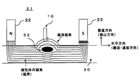
- FIG. 1 is a cross-sectional view of a magnetic flux leakage detecting device according to a first embodiment. Sectional drawing explaining the excitation to a magnetic body and leakage flux detection by the leakage flux detection apparatus of FIG.
- the top view of the magnetic sensor module which comprises the magnetic flux leakage detection apparatus shown in FIG.
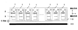
- the top view which expands and shows the TMR magnetic sensor and magnetic line sensor which are the sensor chips which comprise the magnetic sensor module shown in FIG.
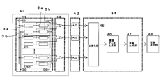
- FIG. 4 is a circuit diagram of the magnetic sensor module shown in FIG. 3 and an image device connected to the magnetic sensor module.
- FIG. 6 is a circuit diagram of a magnetic sensor module according to a second embodiment and an image device connected to the magnetic sensor module.
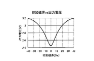
- FIG. 3 is an output characteristic diagram of the magnetic sensor module according to Example 1 (applied magnetic field ⁇ 40 Oe to 40 Oe).
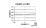
- FIG. 3 is an output characteristic diagram of the magnetic sensor module according to Example 1 (applied magnetic field—0.5 Oe to 0.5 Oe).
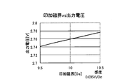
- FIG. 3 is an output characteristic diagram of the magnetic sensor module according to Example 1 (applied magnetic field: 9.5 Oe to 10.5 Oe).
- FIG. 6 is a characteristic diagram illustrating an output voltage at the time of air gap detection in each sensitivity region of the magnetic sensor module according to the first embodiment.
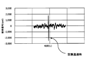
- FIG. 6 is a waveform diagram of a detection signal when the magnetic line sensor that constitutes the magnetic sensor module according to the first embodiment detects a gap in the magnetic body.
- FIG. 6 is a distribution diagram of a bias magnetic field applied to a magnetic line sensor by a bias applying unit and a relationship diagram between an excitation yoke position and a magnetic flux density.
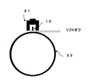
- Sectional drawing of the leakage magnetic flux detection apparatus which shows another Example of a magnetic body.
- the top view of the magnetic sensor module which shows a magnetic body as a cross section similarly to FIG.
- the present invention uses a TMR magnetic sensor (referred to as a “magnetic line sensor”) arranged in a line to detect leakage magnetic flux caused by internal inclusions, scratches, air gaps, etc. of a magnetic material such as a thin steel plate.
- a magnetic line sensor arranged in a line to detect leakage magnetic flux caused by internal inclusions, scratches, air gaps, etc. of a magnetic material such as a thin steel plate.
- the present invention relates to a method of detecting leakage magnetic flux of a magnetic material with high sensitivity by effectively utilizing the characteristics of the TMR magnetic sensor.
- the leakage magnetic flux detection device in this embodiment uses a magnetizer 21 that excites a thin steel plate 30 that is a magnetic material, and leakage magnetic flux caused by internal inclusions, scratches, air gaps, and the like of the thin steel plate 30.
- a magnetic sensor module 20 (see FIG. 3) in which a magnetic line sensor 10 in which a plurality of TMR magnetic sensors 1 to be detected (see FIG. 4) are arranged in a line is mounted on the wiring board 5 and the magnetic sensing direction of the TMR magnetic sensor 1 are arranged.
- Bias applying means for applying a bias magnetic field The magnetizer 21 also serves as the bias applying means.
- the magnetic sensor module 20 is shown in FIG. Formed on one side of the wiring board 5 is a magnetic line sensor 10 composed of a number of TMR magnetic sensors 1 arranged close to the edge. Since each TMR magnetic sensor 1 is configured as a sensor chip, it may be referred to as a sensor chip 1 below.
- the thin steel plate 30 as an object is arranged close to one side where the magnetic line sensor 10 including the plurality of TMR magnetic sensors 1 of the wiring board 5 is formed.
- the wiring substrate 5 is formed with an amplifying unit 11 made of an amplifier IC or an amplifier chip.
- the position of the amplifying unit 11 is not particularly limited, but is preferably close to the magnetic line sensor 10.
- a terminal portion 7 is provided on the other side of the wiring board 5.
- the side on which the terminal portion 7 is provided is not limited, but in this embodiment, the magnetic line sensor 10 is provided on the opposite side of the side formed in proximity.
- a lead 18 extends from the terminal portion 7 to the outside of the magnetic sensor module 20, and a signal obtained by the magnetic line sensor 10 is transferred from the terminal portion 7 to the lead 18 via wiring inside the wiring board 5. Reportedly. FIG.
- FIG. 4 shows an enlarged plan view of a part of the wiring board 5 on which the magnetic line sensor 10 composed of the arranged TMR magnetic sensors 1 is formed.
- the leakage magnetic flux detection device needs to be brought close to the thin steel plate 30 to be conveyed, which is an object, at the time of measurement.
- the end of each TMR magnetic sensor 1 is located on the edge of the wiring board 5, which is a component of the magnetic sensor module 20. Need to be close.
- the distance from the edge to the end is set to 0.05 mm.
- the magnetic line sensor 10 is formed by arranging a large number of TMR magnetic sensors 1 having the same configuration on the main surface of the wiring board 5 on a straight line at a narrow pitch.
- Each TMR magnetic sensor 1 is composed of a fixed resistor or a low-sensitivity TMR element 2 and a high-sensitivity TMR element 3 having the same configuration, and between both elements 2 and 3 in which output terminals OUT common to both elements 2 and 3 are connected in series.
- the power supply terminal VDD is connected to the high-sensitivity TMR element 3 and disposed at the one end side in the longitudinal direction
- the ground terminal GND is disposed at the low-sensitivity TMR element 2 is connected to the one end side (see FIG. 5).
- the number of TMR magnetic sensors 1 in the magnetic line sensor 10 is 154
- the pitch in the width direction of the TMR magnetic sensor elements 2 and 3 in the magnetic line sensor 10 is 0.5 mm.
- the other end side opposite to the one end in the longitudinal direction of the TMR magnetic sensor 1 coincides with the side where the wiring board 5 faces the thin steel plate 30.
- Each TMR magnetic sensor 1 is arranged in a line along a side facing the thin steel plate 30 of the wiring board 5 to constitute the magnetic line sensor 10.
- the leakage magnetic flux detection device in the present embodiment amplifies the leakage magnetic flux information of the thin steel plate 30 obtained by the TMR magnetic sensor 1 and sends it from the terminal section 7 to the image processing device, and the leakage magnetic flux information sent by this image processing device. Can be imaged.
- each TMR magnetic sensor 1 in the magnetic line sensor 10 is referred to as a channel (hereinafter sometimes referred to as “ch”), and is arranged from the channel 1 to the channel 154 from the top to the bottom in FIG. Then, this is expressed as 1ch, 2ch, 3ch, ..., 154ch.
- an analog signal from the magnetic line sensor 10 is input from the output terminal OUT (see FIG. 4) of each TMR magnetic sensor 1 to each amplifier constituting the amplifying unit 11.
- the output of each amplifier is input to each A / D converter of the A / D converter 12 of the image processing apparatus and is digitally converted.
- the digital signal digitally converted by the A / D conversion unit 12 is input to the image processing unit 13 to generate an image, and the generated image is displayed on the image display unit 17.
- the image processing unit 13 normalizes the digitized TMR magnetic sensor output so as to eliminate variations among the channels 1 to 154, and quantizes the normalized digital signal between the maximum value and the minimum value.
- a gradation data generation unit 15 that generates gradation data by converting the image data
- an image generation unit 16 that generates an image based on the gradation data in each of the channels 1 to 154.
- FIG. 1 a thin steel plate 30 as an object travels on a roll 31.
- the magnetizer 21 is disposed close to the thin steel plate 30 on the roll 31.
- the magnetic line sensor 10 is disposed between the excitation yoke N pole 22 and S pole 23 of the magnetizer 21.
- a magnetic body magnetic flux that is, a magnetic field is formed inside the thin steel plate 30 by the excitation yokes 22 and 23.
- FIG. 2 if there is a non-magnetic inclusion 32 inside the thin steel plate 30, leakage magnetic flux is generated from that portion and is detected by the magnetic line sensor 10.
- the magnetizer 21 also serves as a bias applying means for applying a bias magnetic field in the magnetic sensing direction of the TMR magnetic sensor 1 as shown in FIGS.
- the bias applying means may use another magnetizing device instead of the magnetizer 21, or a permanent magnet may be added as a bias applying auxiliary means in addition to the magnetizer 21.
- the thin steel plate 30 is magnetized by the magnetizer 21, and the low sensitivity region near 0 Oersted in the magnetic sensing direction of the TMR magnetic sensor 1 by the magnetizer 21 also serving as the bias applying means.
- the bias magnetic field (spatial magnetic flux) is applied so that the sensitivity of the TMR magnetic sensor 1 is in a high sensitivity region that is a linear region.
- FIG. 7 shows output characteristics of the magnetic sensor module 20 on which the TMR magnetic sensor 1 is mounted.
- the horizontal axis represents the magnetic field (Oe) applied to the TMR magnetic sensor 1 of the magnetic sensor module 20, and the vertical axis represents the output voltage (V) from the output terminal OUT (see FIG. 4) that reacts to the applied magnetic field.
- the power supply voltage is 5 V, and the value obtained by multiplying the output of the TMR magnetic sensor 10 times by the amplifying unit 11 is described as the output voltage.
- FIG. 7 shows the sensitivity characteristics in the region of the applied magnetic field ⁇ 40 to 40 Oe.
- a region of ⁇ 2 to 2 Oe is a low sensitivity region, and the characteristic diagram of FIG. 8 is included in the region.
- the region of 2 to 13 Oe is the high sensitivity region, and the characteristic diagram of FIG. 9 is included in the region.
- the TMR magnetic sensor 1 is used in this high sensitivity region.
- FIG. 10 shows the relationship between the output (vertical axis: output voltage) and the magnetomotive force (horizontal axis) at the time of air gap detection in each sensitivity region of the TMR magnetic sensor 1 of the magnetic sensor module 20.
- a region showing high sensitivity is a region indicated by ⁇ , and the TMR magnetic sensor 1 is used in this high sensitivity region as described above.
- FIG. 11 illustrates the state of the detection signal.
- FIG. 12A is a distribution diagram of a bias magnetic field applied to the magnetic line sensor 10 in which the magnetizer 21 has the sensor chip 1 arranged
- FIG. 12B is a relationship diagram between the positions of the excitation yokes 22 and 23 and the magnetic flux density. is there.
- the magnetic field sensor 10 of the magnetic sensor module 20 has a high sensitivity where the sensitivity of the TMR magnetic sensor 1 adjacent to the low sensitivity region near 0 Oersted is in the linear region so that the magnetic line sensor 10 can be used with high sensitivity. It is applied so as to be a sensitivity region.
- the plurality of TMR magnetic sensors 1 constituting the magnetic line sensor 10 are perpendicular to the width direction of the thin steel plate 30, in other words, the moving direction of the thin steel plate 30. Is excited in the direction perpendicular to the width direction, in other words, the moving direction.
- the magnetic sensor module 20 is located at a position slightly away from the center position between the N pole 22 and the S pole 23 of the magnetizer 21 (near the bias magnetic field 7Oe).
- the magnetic line sensor 10 is preferably arranged.
- the thin steel plate 30 in the method of detecting the leakage magnetic flux of the thin steel plate 30, the thin steel plate 30 is magnetized by the magnetizer 21, and the magnetism 21 near the 0 Oersted in the magnetic sensitive direction of the TMR magnetic sensor 1.
- a bias magnetic field is applied beyond the low sensitivity region so that the sensitivity of the TMR magnetic sensor 1 is a high sensitivity region that is a linear region. Thereby, the maximum sensitivity of the magnetic line sensor 10 can be extracted.
- the magnetic body in a present Example is not limited to the above-mentioned thin steel plate 30,
- the processed goods of the thin steel plate 30 are also included.
- a steel plate processed product 33 such as a can or a case formed from the thin steel plate 30 into a cylindrical shape or a bottomed cylindrical shape is also a target.
- the steel plate processed product 33 is supported on the rotary head 35 of the rotating device 34 so that the cylindrical axis coincides with the rotation axis, and the outer periphery of the magnetic line sensor 10 and the magnetizer 21 and the steel plate processed product 33 facing the magnetic line sensor 10.
- the planes are set so as to have the same arrangement relationship as in FIG. As shown in FIG.
- the magnetic line sensor 10 arranged in the rotation axis direction that is a direction perpendicular to the moving direction causes the surface of the steel plate processed product 33 to Scan to detect leakage flux. Similar to FIGS. 1 and 2, if there is a non-magnetic inclusion 32 in the steel plate processed product 33, this inclusion 32 can be detected. Similarly to FIGS. 10 and 11, the steel plate If there is a gap inside the processed product 33, this gap can be detected. Furthermore, it goes without saying that the present invention can be applied to magnetic bodies other than steel plates.
- Embodiment 2 will be described with reference to FIG.
- the magnetic line sensor 10 two different types of TMR elements constitute one channel (indicated as ch in FIG. 6), and two output terminals OUT (see FIG. 4) are respectively connected to the same amplifier of the amplifier 42. Connected to two input terminals.
- each of the channels 1 to 154 has a bridge structure, and the number of TMR magnetic sensors 1 in this embodiment is 154 ch ⁇ 2, that is, twice as many as 308 in comparison with the first embodiment.
- the analog signal from the magnetic line sensor 10 is input from the output terminal OUT (see FIG. 4) of each TMR magnetic sensor 1 to each amplifier constituting the amplifying unit 42.
- the output of each amplifier is input to each A / D converter of the A / D converter 43 of the image processing apparatus and is digitally converted.
- the digital signal digitally converted by the A / D conversion unit 43 is input to the image processing unit 44 to generate an image, and the generated image is displayed on the image display unit 48.
- the image processing unit 44 normalizes the digitized TMR magnetic sensor output so as to eliminate variations among the channels 1 to 154, and quantizes the normalized digital signal between the maximum value and the minimum value.
- a gradation data generation unit 46 that generates gradation data by converting the image data into a grayscale data, and an image generation unit 47 that generates an image based on the gradation data in each of the channels 1 to 154.
- a full-bridge structure has been described, but this structure can be operated differentially.
- the detection of the leakage magnetic flux due to inclusions, scratches, air gaps and the like inherent in the magnetic material such as the thin steel plate is reliably and efficiently performed. Can be done.
Landscapes
- Chemical & Material Sciences (AREA)
- Chemical Kinetics & Catalysis (AREA)
- Electrochemistry (AREA)
- Physics & Mathematics (AREA)
- Health & Medical Sciences (AREA)
- Life Sciences & Earth Sciences (AREA)
- Analytical Chemistry (AREA)
- Biochemistry (AREA)
- General Health & Medical Sciences (AREA)
- General Physics & Mathematics (AREA)
- Immunology (AREA)
- Pathology (AREA)
- Investigating Or Analyzing Materials By The Use Of Magnetic Means (AREA)
Abstract
【課題】 TMR磁気センサを磁気センサとして高感度で用いることによって特性を向上させた磁性体の漏洩磁束検出装置及び漏洩磁束検出方法を提供する。 【解決手段】 漏洩磁束検出装置は、磁性体30を励磁する磁化器21、磁性体30の内部介在物・キズ・空隙等に起因した漏洩磁束を検出する複数のTMR磁気センサをライン状に配列してなる磁気ラインセンサ10を有する磁気センサモジュール20と、前記磁気ラインセンサ10の感磁方向にバイアス磁界を印加するバイアス付与手段とを有し、バイアス付与手段によってTMR磁気センサの感磁方向に0エルステッド付近の低感度領域を超えて、TMR磁気センサの感度が線形領域の範囲である高感度領域となるようにバイアス磁界を印加する。
Description
本発明は、磁気センサを用いた磁性体の内部介在物・キズ・空隙などに起因した漏洩磁束を検出する装置及び方法に関するものである。
従来、磁気センサを用いる検査装置は、漏洩磁束などの磁気特性を検出するものであるが、検査の対象としては磁性を有する磁性体或いは非磁性体がある。また、磁気センサとしては、ホール素子やTMR(Tunneling Magneto Resistance)素子、その他の素子を用いた磁気センサが知られている。特許文献1には、磁気ラインセンサを用いて、非磁性体である紙幣や有価証券等の紙葉類に磁気インクで印刷された磁気パターンを検出することが記載されている。前記磁気ラインセンサは、回路基板の表面側に、磁性体に対する感磁方向が長手方向である磁気センサ素子が、センサ素子長手方向に対して垂直に狭ピッチで多数配置されて構成される。また、前記回路基板の裏面側には、各磁気センサ素子にバイアス磁界を加える永久磁石が配置されている。
特許文献1に記載された発明は、分解能を高めて、磁気パターンをその存在を検出するだけではなく、磁気画像としての検出にも適用できる磁気ラインセンサを提供するものであって、当該磁気ラインセンサは、磁性体の感磁方向が長手方向である磁気センサ素子を用いた磁気センサを磁気センサ素子の長手方向に対してほぼ垂直に狭ピッチで多数配置してなるものである。この磁気ラインセンサは、磁気パターンを設けた被検出媒体の搬送方向と磁気センサ素子の長手方向が一致するように配置して使用する。
また、特許文献2には、磁性体である薄鋼板の表面や内部の欠陥検出において、磁気センサを用いて磁場を検出する漏洩磁束探傷法に係る発明が開示されている。この発明は、試験体を磁化する磁化器と、欠陥に起因して発生した磁場を検出する磁気検出部と、前記磁気検出部に対応した発光素子を備えた磁気探傷用プローブを有し、前記磁気検出部からの出力信号の演算結果により、前記発光素子の点灯を判定する機能を備えた磁場可視化センサ及び当該磁場可視化センサを備えた磁気探傷用プローブを提供するものである。この発明は、磁化器から磁気センサに漏洩する磁束と試験体内の欠陥に起因して試験体外に漏洩する磁束を識別し、さらに欠陥をその場で視認できる機能を有する。
特許文献1の磁気ラインセンサは、非磁性体である紙葉類に磁気インクで印刷された磁気パターンを検出することを目的とするものであって、特許文献1には、磁性体(例えば薄鋼板)の製造時に内在する異物に対する検査については何も記載されていない。特許文献1の磁気ラインセンサを磁性体の内部介在物・キズ・空隙などの検査に適用した場合には、このような検査に精度よく適合するように、磁性体とセンサとの位置関係、素子構成、磁界印加手段などについて創意工夫をする必要がある。また、特許文献2に記載された漏洩磁束探傷法を磁性体の内部介在物・キズ・空隙などの検査に適用するためには、基板デザイン、素子構成、磁界印加手段等において更なる創意工夫が必要である。
また、特許文献1に開示された発明では、TMR磁気センサを用いて発明を説明しているが、使用される磁気センサは、これに限るものではないとしている(特許文献1の段落0028参照)。また、特許文献2に開示された発明では、ホール素子を用いて発明を説明しているが、磁気センサは、ホール素子に限るものではないとしている(特許文献2の段落0014参照)。ホール素子は、磁気センサとして、良好な直線性感度を有しているが、感度が低く、周辺温度の影響を受け易いという短所がある。これに対して、前記TMR磁気センサは、高感度であり、温度特性に優れている。
本発明は、このような事情によりなされたものであり、TMR磁気センサを磁気センサとして高感度で用いることによって特性を向上させた磁性体の漏洩磁束検出装置及びこの検出装置を使用した漏洩磁束検出方法を提供するものである。
本発明は、このような事情によりなされたものであり、TMR磁気センサを磁気センサとして高感度で用いることによって特性を向上させた磁性体の漏洩磁束検出装置及びこの検出装置を使用した漏洩磁束検出方法を提供するものである。
本発明の磁性体の漏洩磁束検出装置の一態様は、磁性体を励磁する磁化器と、前記磁性体に対向配置されて前記磁性体の内部介在物・キズ・空隙などに起因した漏洩磁束を検出するTMR磁気センサを有する磁気センサモジュールと、前記TMR磁気センサの感磁方向にバイアス磁界を印加するバイアス付与手段とを備えたことを特徴としている。前記バイアス付与手段は、前記磁化器が兼ねると好適であるが、磁化器に加えて永久磁石などのバイアス付与補助手段を有するようにしても良い。前記磁気センサモジュールは、前記複数のTMR磁気センサを搭載する配線基板を有し、前記磁性体と前記TMR磁気センサを構成するセンサチップとの距離を小さくするために、当該センサチップを前記磁性体の表面に対向する前記配線基板の端部に沿って複数配置するようにしても良い。前記磁気センサモジュールを高感度で使用できるように、前記バイアス付与手段によってTMR磁気センサに印加されるバイアス磁界が0Oe(以下「エルステッド」という場合もある。)付近の低感度領域に隣接する前記TMR磁気センサの感度が線形領域の範囲である高感度領域となるように印加されるようにしても良い。前記磁性体からの垂直方向の漏洩磁束を検出するために、前記複数のTMR磁気センサは、前記磁性体の動く方向と直角の方向に配置され、前記動く方向に励磁されるようにしても良い。前記磁気センサモジュールの感度が最も高い付近にバイアス磁界を与えるために、前記磁化器のN極とS極の間の中心位置から適正に離れた位置に当該磁気センサモジュールを配置するようにしても良い。
本発明の磁性体の漏洩磁束検出方法の一態様は、上述のように構成した漏洩磁束検出装置を用いて前記磁性体の漏洩磁束を検出する方法において、前記磁化器により前記磁性体を磁化すると共に、前記バイアス付与手段によって前記TMR磁気センサの感磁方向に0エルステッド付近の低感度領域を超えて、前記TMR磁気センサの感度が線形領域の範囲である高感度領域となるようにバイアス磁界を印加することを特徴としている。
本発明の磁性体の漏洩磁束検出装置は、TMR磁気センサを磁気センサとして高感度状態で用いることによって特性を向上させ、磁性体の漏洩磁束を確実に検出することができ、また、本発明の漏洩磁束検出方法によれば、この漏洩磁束検出装置を使用して磁性体の漏洩磁束を高感度に検出することができる。
本発明は、ライン状に配列されたTMR磁気センサ(「磁気ラインセンサ」という。)を用いて薄鋼板などの磁性体の内部介在物・キズ・空隙などに起因した漏洩磁束を検出する漏洩磁束検出装置に関するとともに、前記TMR磁気センサの特性を有効に利用して磁性体の漏洩磁束を高感度に検出する方法に関するものである。
以下、図1-図5、図7-図12を参照して実施例1を説明する。
この実施例における漏洩磁束検出装置は、図1に示すように、磁性体である薄鋼板30を励磁する磁化器21と、薄鋼板30の内部介在物・キズ・空隙などに起因した漏洩磁束を検出する複数のTMR磁気センサ1(図4参照)をライン状に配列した磁気ラインセンサ10を配線基板5に搭載した磁気センサモジュール20(図3参照)と、TMR磁気センサ1の感磁方向にバイアス磁界を印加するバイアス付与手段とを備えている。このバイアス付与手段は、前記磁化器21が兼ねている。また、31は図1上時計方向に回転可能なロールであり、このロール31にガイドされて、前記薄鋼板30は前記ロール31を含む図示していない搬送装置により図1上右方向に搬送される。
磁気センサモジュール20は、図3に示されている。配線基板5の一辺には、その縁に近接して配列された多数のTMR磁気センサ1からなる磁気ラインセンサ10が形成されている。各TMR磁気センサ1は、センサチップとして構成されているので、以下にはセンサチップ1という場合もある。この漏洩磁束検出装置による測定時には対象物の薄鋼板30が配線基板5の複数のTMR磁気センサ1からなる磁気ラインセンサ10が形成された1辺に近接して配置される。また、配線基板5にはアンプICもしくはアンプチップからなる増幅部11が形成されている。増幅部11の位置は、特に限定されないが、磁気ラインセンサ10に近接していることが望ましい。配線基板5の他の辺には端子部7が設けられている。端子部7が設けられる辺は限定されないが、本実施例では、磁気ラインセンサ10が近接して形成されている辺の対向辺に設けられている。端子部7からは、リード18が前記磁気センサモジュール20の外部に延びており、磁気ラインセンサ10によって得られた信号は、配線基板5内部の配線を介して前記端子部7から前記リード18に伝えられる。
配列されたTMR磁気センサ1からなる磁気ラインセンサ10が形成された配線基板5の一部を拡大した平面図が図4に示されている。
図4において、漏洩磁束検出装置は、測定時、対象物である搬送される薄鋼板30に近接させる必要がある。薄鋼板30の磁気特性、漏洩磁束を効率良く有効に検出するには、磁気センサモジュール20の構成要素である配線基板5の薄鋼板30に近接対向する辺縁に各TMR磁気センサ1の端部を近づける必要がある。図4では前記辺縁から前記端部までの距離を0.05mmにしている。
この実施例における漏洩磁束検出装置は、図1に示すように、磁性体である薄鋼板30を励磁する磁化器21と、薄鋼板30の内部介在物・キズ・空隙などに起因した漏洩磁束を検出する複数のTMR磁気センサ1(図4参照)をライン状に配列した磁気ラインセンサ10を配線基板5に搭載した磁気センサモジュール20(図3参照)と、TMR磁気センサ1の感磁方向にバイアス磁界を印加するバイアス付与手段とを備えている。このバイアス付与手段は、前記磁化器21が兼ねている。また、31は図1上時計方向に回転可能なロールであり、このロール31にガイドされて、前記薄鋼板30は前記ロール31を含む図示していない搬送装置により図1上右方向に搬送される。
磁気センサモジュール20は、図3に示されている。配線基板5の一辺には、その縁に近接して配列された多数のTMR磁気センサ1からなる磁気ラインセンサ10が形成されている。各TMR磁気センサ1は、センサチップとして構成されているので、以下にはセンサチップ1という場合もある。この漏洩磁束検出装置による測定時には対象物の薄鋼板30が配線基板5の複数のTMR磁気センサ1からなる磁気ラインセンサ10が形成された1辺に近接して配置される。また、配線基板5にはアンプICもしくはアンプチップからなる増幅部11が形成されている。増幅部11の位置は、特に限定されないが、磁気ラインセンサ10に近接していることが望ましい。配線基板5の他の辺には端子部7が設けられている。端子部7が設けられる辺は限定されないが、本実施例では、磁気ラインセンサ10が近接して形成されている辺の対向辺に設けられている。端子部7からは、リード18が前記磁気センサモジュール20の外部に延びており、磁気ラインセンサ10によって得られた信号は、配線基板5内部の配線を介して前記端子部7から前記リード18に伝えられる。
配列されたTMR磁気センサ1からなる磁気ラインセンサ10が形成された配線基板5の一部を拡大した平面図が図4に示されている。
図4において、漏洩磁束検出装置は、測定時、対象物である搬送される薄鋼板30に近接させる必要がある。薄鋼板30の磁気特性、漏洩磁束を効率良く有効に検出するには、磁気センサモジュール20の構成要素である配線基板5の薄鋼板30に近接対向する辺縁に各TMR磁気センサ1の端部を近づける必要がある。図4では前記辺縁から前記端部までの距離を0.05mmにしている。
図4に示すように、磁気ラインセンサ10は、配線基板5の主面に同一構成のTMR磁気センサ1を多数、狭ピッチで一直線上に配置してなるものである。各TMR磁気センサ1は、同一構成の固定抵抗又は低感度TMR素子2と高感度TMR素子3から構成され、両素子2,3共通の出力端子OUTが直列接続された両素子2,3間に形成されてTMR磁気センサ1の長手方向の一端に位置し、電源端子VDDが高感度TMR素子3に接続され前記長手方向の前記一端側に位置して配置され、接地端子GNDが低感度TMR素子2に接続されて前記一端側に接続されている(図5参照)。
ここで、例えば、磁気ラインセンサ10のTMR磁気センサ1数は154個で、磁気ラインセンサ10における各TMR磁気センサ素子2,3の幅方向のピッチは0.5mmである。
TMR磁気センサ1の長手方向の前記一端とは反対側である他端側は、配線基板5が薄鋼板30に対向した辺と一致している。各TMR磁気センサ1は、配線基板5の薄鋼板30と対向する辺に沿って一列に配置されて磁気ラインセンサ10を構成する。
本実施例における漏洩磁束検出装置は、TMR磁気センサ1により得られた薄鋼板30の漏洩磁束情報を増幅して端子部7から画像処理装置に送り、この画像処理装置で送られた漏洩磁束情報を画像化することができる。
ここで、例えば、磁気ラインセンサ10のTMR磁気センサ1数は154個で、磁気ラインセンサ10における各TMR磁気センサ素子2,3の幅方向のピッチは0.5mmである。
TMR磁気センサ1の長手方向の前記一端とは反対側である他端側は、配線基板5が薄鋼板30に対向した辺と一致している。各TMR磁気センサ1は、配線基板5の薄鋼板30と対向する辺に沿って一列に配置されて磁気ラインセンサ10を構成する。
本実施例における漏洩磁束検出装置は、TMR磁気センサ1により得られた薄鋼板30の漏洩磁束情報を増幅して端子部7から画像処理装置に送り、この画像処理装置で送られた漏洩磁束情報を画像化することができる。
次に、図5の磁気センサモジュール20の回路配線接続図及び画像処理部と画像表示部から構成された画像処理装置のブロック図を参照して、前記磁気センサモジュール20をさらに説明する。
磁気ラインセンサ10において、電源端子VDDから各高感度TMR素子3に電源電圧が供給され、各低感度TMR素子2には接地端子GNDが接続されている。
磁気ラインセンサ10における各TMR磁気センサ1をチャンネル(以下「ch」という場合もある。)と称し、図5上、上から下に向けて、チャンネル1からチャンネル154まで並んでいるが、図5ではこれを1ch、2ch、3ch、・・・、154chと表記している。
磁気ラインセンサ10において、電源端子VDDから各高感度TMR素子3に電源電圧が供給され、各低感度TMR素子2には接地端子GNDが接続されている。
磁気ラインセンサ10における各TMR磁気センサ1をチャンネル(以下「ch」という場合もある。)と称し、図5上、上から下に向けて、チャンネル1からチャンネル154まで並んでいるが、図5ではこれを1ch、2ch、3ch、・・・、154chと表記している。
図5において、磁気ラインセンサ10からのアナログ信号は、各TMR磁気センサ1の出力端子OUT(図4参照)から増幅部11を構成する各増幅器に入力する。
各増幅器の出力は、画像処理装置のA/D変換部12の各A/D変換器に入力されてデジタル変換される。A/D変換部12でデジタル変換されたデジタル信号は、画像処理部13に入力して画像が生成され、生成された画像は画像表示部17に表示される。
画像処理部13は、デジタル化されたTMR磁気センサ出力の各チャンネル1~154間のばらつきをなくすべく正規化する正規化部14と、正規化したデジタル信号を最大値から最小値の間で量子化して階調データを生成する階調データ生成部15と、各チャンネル1~154での階調データに基づいて画像を生成する画像生成部16とからなる。
各増幅器の出力は、画像処理装置のA/D変換部12の各A/D変換器に入力されてデジタル変換される。A/D変換部12でデジタル変換されたデジタル信号は、画像処理部13に入力して画像が生成され、生成された画像は画像表示部17に表示される。
画像処理部13は、デジタル化されたTMR磁気センサ出力の各チャンネル1~154間のばらつきをなくすべく正規化する正規化部14と、正規化したデジタル信号を最大値から最小値の間で量子化して階調データを生成する階調データ生成部15と、各チャンネル1~154での階調データに基づいて画像を生成する画像生成部16とからなる。
次に、図1及び図2を参照して、上述した漏洩磁束検出装置を用いた磁性体の漏洩磁束の検出方法を説明する。
図1に示すように、対象物となる薄鋼板30は、ロール31上を走行している。磁化器21は、ロール31上の薄鋼板30に近接して配置される。そして、磁化器21の励磁ヨークN極22とS極23との間には、磁気ラインセンサ10が配置されている。励磁ヨーク22,23によって、薄鋼板30内部には磁性体内磁束、即ち、磁界が形成される。このとき、図2に示すように、薄鋼板30の内部に非磁性体の介在物32があれば、その部分から漏洩磁束が生じ、磁気ラインセンサ10で検出される。
図1に示すように、対象物となる薄鋼板30は、ロール31上を走行している。磁化器21は、ロール31上の薄鋼板30に近接して配置される。そして、磁化器21の励磁ヨークN極22とS極23との間には、磁気ラインセンサ10が配置されている。励磁ヨーク22,23によって、薄鋼板30内部には磁性体内磁束、即ち、磁界が形成される。このとき、図2に示すように、薄鋼板30の内部に非磁性体の介在物32があれば、その部分から漏洩磁束が生じ、磁気ラインセンサ10で検出される。
次に、TMR磁気センサ1の感磁方向にバイアス磁界を印加するバイアス付与手段は、図2,図12に示すように、この実施例では磁化器21が兼ねている。しかしながら、バイアス付与手段は、磁化器21に換えて他の磁化装置を使用しても良いし、磁化器21に加えてバイアス付与補助手段として永久磁石を付加しても良い。
薄鋼板30の漏洩磁束を検出する方法において、磁化器21により薄鋼板30を磁化すると共に、前記バイアス付与手段を兼ねる磁化器21によってTMR磁気センサ1の感磁方向に0エルステッド付近の低感度領域を超えて、TMR磁気センサ1の感度が線形領域の範囲である高感度領域となるようにバイアス磁界(空間磁束)を印加することを特徴とするものである。
薄鋼板30の漏洩磁束を検出する方法において、磁化器21により薄鋼板30を磁化すると共に、前記バイアス付与手段を兼ねる磁化器21によってTMR磁気センサ1の感磁方向に0エルステッド付近の低感度領域を超えて、TMR磁気センサ1の感度が線形領域の範囲である高感度領域となるようにバイアス磁界(空間磁束)を印加することを特徴とするものである。
以下、図7乃至9を参照して、漏洩磁束検出に用いる磁気センサモジュール20の特性を説明する。
TMR磁気センサ1は、印加磁界(Oe)によって出力電圧が大きく変化する。図7は、TMR磁気センサ1を搭載した磁気センサモジュール20の出力特性を示している。横軸は、磁気センサモジュール20のTMR磁気センサ1に印加された磁界(Oe)、縦軸は、印加された磁界に反応する出力端子OUT(図4参照)からの出力電圧(V)を表わしている。なお、図7、図8、図9は共に、電源電圧が5Vであり、TMR磁気センサ出力を増幅部11で10倍した数値を出力電圧に記載している。
図7では、印加磁界-40~40Oeの領域の感度特性を示している。この感度特性の中で、-2~2Oeの領域が低感度域であり、図8の特性図がその領域に含まれる。また、2~13Oeの領域が高感度域であり、図9の特性図がその領域に含まれる。この実施例ではこの高感度域でTMR磁気センサ1を用いる。
TMR磁気センサ1は、印加磁界(Oe)によって出力電圧が大きく変化する。図7は、TMR磁気センサ1を搭載した磁気センサモジュール20の出力特性を示している。横軸は、磁気センサモジュール20のTMR磁気センサ1に印加された磁界(Oe)、縦軸は、印加された磁界に反応する出力端子OUT(図4参照)からの出力電圧(V)を表わしている。なお、図7、図8、図9は共に、電源電圧が5Vであり、TMR磁気センサ出力を増幅部11で10倍した数値を出力電圧に記載している。
図7では、印加磁界-40~40Oeの領域の感度特性を示している。この感度特性の中で、-2~2Oeの領域が低感度域であり、図8の特性図がその領域に含まれる。また、2~13Oeの領域が高感度域であり、図9の特性図がその領域に含まれる。この実施例ではこの高感度域でTMR磁気センサ1を用いる。
次に、薄鋼板30内の空隙(図示せず)を検出した場合の磁気センサモジュール20の動作を説明する。図10は、磁気センサモジュール20のTMR磁気センサ1の各感度領域における空隙検出時の出力(縦軸:出力電圧)とその起磁力(横軸)との関係を表わしている。ここで、高い感度を示す領域は●で示す領域であり、上述したように、この高感度領域でTMR磁気センサ1を用いる。図11は、検出信号の状態を説明するものであり、漏洩磁束検出装置を動作させ、ロール31でガイドして薄鋼板30を所定方向に搬送する(図1参照)と、空隙通過時に漏洩磁束が生じることで、磁気ラインセンサ10の出力電圧が大きく変化し、空隙が検出される。
図12(a)は磁化器21がセンサチップ1を配列してなる磁気ラインセンサ10に与えるバイアス磁界の分布図で、図12(b)は励磁ヨーク22,23位置と磁束密度の関係図である。図12において、磁気センサモジュール20の磁気ラインセンサ10を高感度で使用できるように、バイアス磁界が、0エルステッド付近の低感度領域に隣接するTMR磁気センサ1の感度が線形領域の範囲である高感度領域となるように印加される。
薄鋼板30からの垂直方向の漏洩磁束を検出するために、磁気ラインセンサ10を構成する複数のTMR磁気センサ1は前記薄鋼板30の幅方向、換言すると薄鋼板30の動く方向とは直角の方向に配置され、前記幅方向とは直角の方向、換言すると前記動く方向に励磁される。
磁気ラインセンサ10の感度が最も高い付近にバイアス磁界を与えるために、磁化器21のN極22とS極23の間の中心位置から少し離れた位置(バイアス磁界7Oe付近)に磁気センサモジュール20、とりわけ磁気ラインセンサ10を配置すると良い。
以上、総合するとこの実施例では、薄鋼板30の漏洩磁束を検出する方法において、磁化器21により薄鋼板30を磁化すると共に、磁化器21によってTMR磁気センサ1の感磁方向に0エルステッド付近の低感度領域を超えて、TMR磁気センサ1の感度が線形領域の範囲である高感度領域となるようにバイアス磁界を印加する。これにより、磁気ラインセンサ10の最大感度が引き出せる。
薄鋼板30からの垂直方向の漏洩磁束を検出するために、磁気ラインセンサ10を構成する複数のTMR磁気センサ1は前記薄鋼板30の幅方向、換言すると薄鋼板30の動く方向とは直角の方向に配置され、前記幅方向とは直角の方向、換言すると前記動く方向に励磁される。
磁気ラインセンサ10の感度が最も高い付近にバイアス磁界を与えるために、磁化器21のN極22とS極23の間の中心位置から少し離れた位置(バイアス磁界7Oe付近)に磁気センサモジュール20、とりわけ磁気ラインセンサ10を配置すると良い。
以上、総合するとこの実施例では、薄鋼板30の漏洩磁束を検出する方法において、磁化器21により薄鋼板30を磁化すると共に、磁化器21によってTMR磁気センサ1の感磁方向に0エルステッド付近の低感度領域を超えて、TMR磁気センサ1の感度が線形領域の範囲である高感度領域となるようにバイアス磁界を印加する。これにより、磁気ラインセンサ10の最大感度が引き出せる。
なお、本実施例における磁性体は、上述の薄鋼板30に限定されず、薄鋼板30の加工品も含まれる。具体的には、例えば、図13及び図14に示すように、薄鋼板30から円筒状や有底円筒状に成型加工された、缶やケース等の鋼板加工品33も対象となる。鋼板加工品33は回転装置34の回転ヘッド35に、円筒軸が回転軸と一致するように支持され、磁気ラインセンサ10及び磁化器21と鋼板加工品33の前記磁気ラインセンサ10に対向する外周面が、図1と同様の配置関係となるように設定されている。図14に示すように、回転装置34によって鋼板加工品33が回転されることによって、動く方向と直角の方向である回転軸方向に配置された磁気ラインセンサ10が、鋼板加工品33の表面を走査して漏洩磁束を検出する。図1及び図2と同様に、鋼板加工品33の内部に非磁性体の介在物32があれば、この介在物32を検出することができ、また、図10及び図11と同様に、鋼板加工品33の内部に空隙があれば、この空隙を検出することができる。
さらに、鋼板以外の磁性体にも本発明を適用可能なことはもちろんである。
さらに、鋼板以外の磁性体にも本発明を適用可能なことはもちろんである。
次に、図6を参照して実施例2を説明する。
実施例1を説明する図5と同様に、磁気センサモジュール40の回路配線接続図及び画像処理部44と画像表示部48から構成された画像処理装置のブロック図を参照してこの実施例の磁気センサモジュール40を説明する。
磁気ラインセンサ10において、種類の異なる2対のTMR素子が1つのチャンネル(図6ではchと表示)を構成し、2つの出力端子OUT(図4参照)は、それぞれ増幅部42の同じ増幅器の2つの入力端子に接続される。一対のTMR素子は、電源端子VDDから高感度TMR素子3aに電源電圧が供給され、低感度TMR素子2aには接地端子GNDが接続されている。もう一方のTMR素子の対は、電源端子VDDから低感度TMR素子2bに電源電圧が供給され、高感度TMR素子3bには接地端子GNDが接続されている。つまり、各チャンネル1~154はブリッジ構造であり、本実施例におけるTMR磁気センサ1の数は、実施例1と比較して、154ch×2個、すなわち2倍の308個必要になる。
実施例1を説明する図5と同様に、磁気センサモジュール40の回路配線接続図及び画像処理部44と画像表示部48から構成された画像処理装置のブロック図を参照してこの実施例の磁気センサモジュール40を説明する。
磁気ラインセンサ10において、種類の異なる2対のTMR素子が1つのチャンネル(図6ではchと表示)を構成し、2つの出力端子OUT(図4参照)は、それぞれ増幅部42の同じ増幅器の2つの入力端子に接続される。一対のTMR素子は、電源端子VDDから高感度TMR素子3aに電源電圧が供給され、低感度TMR素子2aには接地端子GNDが接続されている。もう一方のTMR素子の対は、電源端子VDDから低感度TMR素子2bに電源電圧が供給され、高感度TMR素子3bには接地端子GNDが接続されている。つまり、各チャンネル1~154はブリッジ構造であり、本実施例におけるTMR磁気センサ1の数は、実施例1と比較して、154ch×2個、すなわち2倍の308個必要になる。
磁気ラインセンサ10からのアナログ信号は、各TMR磁気センサ1の出力端子OUT(図4参照)から増幅部42を構成する各増幅器に入力する。
各増幅器の出力は、画像処理装置のA/D変換部43の各A/D変換器に入力されてデジタル変換される。A/D変換部43でデジタル変換されたデジタル信号は、画像処理部44に入力して画像が生成され、生成された画像は、画像表示部48に表示される。画像処理部44は、デジタル化されたTMR磁気センサ出力の各チャンネル1~154間のばらつきをなくすべく正規化する正規化部45と、正規化したデジタル信号を最大値から最小値の間で量子化して階調データを生成する階調データ生成部46と、各チャンネル1~154での階調データに基づいて画像を生成する画像生成部47とからなる。
この実施例ではフルブリッジ構造を説明したが、この構造は、差動動作させることが出来る。
各増幅器の出力は、画像処理装置のA/D変換部43の各A/D変換器に入力されてデジタル変換される。A/D変換部43でデジタル変換されたデジタル信号は、画像処理部44に入力して画像が生成され、生成された画像は、画像表示部48に表示される。画像処理部44は、デジタル化されたTMR磁気センサ出力の各チャンネル1~154間のばらつきをなくすべく正規化する正規化部45と、正規化したデジタル信号を最大値から最小値の間で量子化して階調データを生成する階調データ生成部46と、各チャンネル1~154での階調データに基づいて画像を生成する画像生成部47とからなる。
この実施例ではフルブリッジ構造を説明したが、この構造は、差動動作させることが出来る。
以上、これらの実施例で説明したとおり、TMR磁気センサで構成される磁気ラインセンサにおいて、薄鋼板などの磁性体に内在する介在物・キズ・空隙などによる漏洩磁束の検出を、確実かつ効率的に行うことができる。
1・・・TMR磁気センサ
2,2a,2b・・・低感度TMR素子
3,3a,3b・・・高感度TMR素子
5・・・配線基板
7・・・端子部
10・・・磁気ラインセンサ
11,42・・・増幅部
12,43・・・A/D変換部
13,44・・・画像処理部
14,45・・・正規化部
15,46・・・階調データ生成部
16,47・・・画像生成部
17,48・・・画像表示部
20,40・・・磁気センサモジュール
21・・・磁化器
22・・・励磁ヨーク(N極)
23・・・励磁ヨーク(S極)
30・・・薄鋼板
31・・・ロール
32・・・介在物
33・・・鋼板加工物
34・・・回転装置
35・・・回転ヘッド
2,2a,2b・・・低感度TMR素子
3,3a,3b・・・高感度TMR素子
5・・・配線基板
7・・・端子部
10・・・磁気ラインセンサ
11,42・・・増幅部
12,43・・・A/D変換部
13,44・・・画像処理部
14,45・・・正規化部
15,46・・・階調データ生成部
16,47・・・画像生成部
17,48・・・画像表示部
20,40・・・磁気センサモジュール
21・・・磁化器
22・・・励磁ヨーク(N極)
23・・・励磁ヨーク(S極)
30・・・薄鋼板
31・・・ロール
32・・・介在物
33・・・鋼板加工物
34・・・回転装置
35・・・回転ヘッド
Claims (7)
- 磁性体を励磁する磁化器と、前記磁性体に対向配置されて前記磁性体の内部介在物・キズ・空隙などに起因した漏洩磁束を検出するTMR磁気センサを有する磁気センサモジュールと、前記TMR磁気センサの感磁方向にバイアス磁界を印加するバイアス付与手段とを備えたことを特徴とする磁気センサを用いた磁性体の漏洩磁束検出装置。
- 前記バイアス付与手段は、前記磁化器が兼ねるか、または前記磁化器に加えてバイアス付与補助手段を有してなることを特徴とする請求項1に記載の磁気センサを用いた磁性体の漏洩磁束検出装置。
- 前記磁気センサモジュールは、前記複数のTMR磁気センサを搭載する配線基板を有し、前記磁性体と前記TMR磁気センサを構成するセンサチップとの距離を小さくするために、当該センサチップを前記磁性体の表面に対向する前記配線基板の端部に沿って複数配置したことを特徴とする請求項1もしくは請求項2に記載の磁気センサを用いた磁性体の漏洩磁束検出装置。
- 前記磁気センサモジュールを高感度で使用できるように、前記バイアス付与手段によって前記TMR磁気センサに印加されるバイアス磁界が0エルステッド付近の低感度領域に隣接する前記TMR磁気センサの感度が線形領域の範囲である高感度領域となるように印加されることを特徴とする請求項1乃至請求項3のいずれか1項に記載の磁気センサを用いた磁性体の漏洩磁束検出装置。
- 前記磁性体を所定方向に動かして漏洩磁束を検出する装置であり、前記磁性体からの垂直方向の漏洩磁束を検出するために、前記複数のTMR磁気センサは、前記磁性体の動く方向と直角の方向に配置され、前記動く方向に励磁されることを特徴とする請求項1乃至請求項4のいずれか1項に記載の磁気センサを用いた磁性体の漏洩磁束検出装置。
- 前記磁気センサモジュールの感度が最も高い付近にバイアス磁界を与えるために、前記磁化器のN極とS極の間の中心位置から適正に離れた位置に当該磁気センサモジュールを配置することを特徴とする請求項1乃至請求項5のいずれか1項に記載の磁気センサを用いた磁性体の漏洩磁束検出装置。
- 請求項1乃至請求項6のいずれか1項に記載の漏洩磁束検出装置を用いて前記磁性体の漏洩磁束を検出する方法において、前記磁化器により前記磁性体を磁化すると共に、前記バイアス付与手段によって前記TMR磁気センサの感磁方向に0エルステッド付近の低感度領域を超えて、前記TMR磁気センサの感度が線形領域の範囲である高感度領域となるようにバイアス磁界を印加することを特徴とする磁気センサを用いた磁性体の漏洩磁束検出方法。
Applications Claiming Priority (4)
| Application Number | Priority Date | Filing Date | Title |
|---|---|---|---|
| JP2017023678 | 2017-02-10 | ||
| JP2017-023678 | 2017-10-25 | ||
| JP2018-010256 | 2018-01-25 | ||
| JP2018010256A JP7084733B2 (ja) | 2017-02-10 | 2018-01-25 | 磁気センサを用いた磁性体の漏洩磁束検出装置及び漏洩磁束検出方法 |
Publications (1)
| Publication Number | Publication Date |
|---|---|
| WO2018147264A1 true WO2018147264A1 (ja) | 2018-08-16 |
Family
ID=63108214
Family Applications (1)
| Application Number | Title | Priority Date | Filing Date |
|---|---|---|---|
| PCT/JP2018/003984 Ceased WO2018147264A1 (ja) | 2017-02-10 | 2018-02-06 | 磁気センサを用いた磁性体の漏洩磁束検出装置及び漏洩磁束検出方法 |
Country Status (1)
| Country | Link |
|---|---|
| WO (1) | WO2018147264A1 (ja) |
Cited By (1)
| Publication number | Priority date | Publication date | Assignee | Title |
|---|---|---|---|---|
| CN115791954A (zh) * | 2022-11-21 | 2023-03-14 | 合肥中大检测技术有限公司 | 一种具有屏蔽功能的钢管漏磁检测的传感器阵列装置 |
Citations (9)
| Publication number | Priority date | Publication date | Assignee | Title |
|---|---|---|---|---|
| JPH0572180A (ja) * | 1991-09-12 | 1993-03-23 | Nkk Corp | 磁気探傷方法およびその装置 |
| JPH06281625A (ja) * | 1993-03-26 | 1994-10-07 | Nippon Steel Corp | 漏洩磁気探傷装置における感度校正装置 |
| JPH06294853A (ja) * | 1993-04-12 | 1994-10-21 | Nippon Steel Corp | 磁気検出装置 |
| JP2002022705A (ja) * | 2000-07-12 | 2002-01-23 | Uchihashi Estec Co Ltd | 磁気センサ及び磁界検出方法並びに装置 |
| JP2010014701A (ja) * | 2008-06-04 | 2010-01-21 | Toshiba Corp | アレイ型磁気センサ基板 |
| JP2011013087A (ja) * | 2009-07-01 | 2011-01-20 | Okayama Univ | 漏洩磁束探傷方法及び装置 |
| WO2015197239A1 (de) * | 2014-06-27 | 2015-12-30 | Institut Dr. Foerster Gmbh & Co. Kg | Verfahren und vorrichtung zur streuflussprüfung |
| JP2016061709A (ja) * | 2014-09-19 | 2016-04-25 | 株式会社東芝 | アレイ型磁気探傷装置、及びその校正方法 |
| JP2016170059A (ja) * | 2015-03-13 | 2016-09-23 | 三井造船株式会社 | 線状部材の診断装置及び診断方法 |
-
2018
- 2018-02-06 WO PCT/JP2018/003984 patent/WO2018147264A1/ja not_active Ceased
Patent Citations (9)
| Publication number | Priority date | Publication date | Assignee | Title |
|---|---|---|---|---|
| JPH0572180A (ja) * | 1991-09-12 | 1993-03-23 | Nkk Corp | 磁気探傷方法およびその装置 |
| JPH06281625A (ja) * | 1993-03-26 | 1994-10-07 | Nippon Steel Corp | 漏洩磁気探傷装置における感度校正装置 |
| JPH06294853A (ja) * | 1993-04-12 | 1994-10-21 | Nippon Steel Corp | 磁気検出装置 |
| JP2002022705A (ja) * | 2000-07-12 | 2002-01-23 | Uchihashi Estec Co Ltd | 磁気センサ及び磁界検出方法並びに装置 |
| JP2010014701A (ja) * | 2008-06-04 | 2010-01-21 | Toshiba Corp | アレイ型磁気センサ基板 |
| JP2011013087A (ja) * | 2009-07-01 | 2011-01-20 | Okayama Univ | 漏洩磁束探傷方法及び装置 |
| WO2015197239A1 (de) * | 2014-06-27 | 2015-12-30 | Institut Dr. Foerster Gmbh & Co. Kg | Verfahren und vorrichtung zur streuflussprüfung |
| JP2016061709A (ja) * | 2014-09-19 | 2016-04-25 | 株式会社東芝 | アレイ型磁気探傷装置、及びその校正方法 |
| JP2016170059A (ja) * | 2015-03-13 | 2016-09-23 | 三井造船株式会社 | 線状部材の診断装置及び診断方法 |
Cited By (1)
| Publication number | Priority date | Publication date | Assignee | Title |
|---|---|---|---|---|
| CN115791954A (zh) * | 2022-11-21 | 2023-03-14 | 合肥中大检测技术有限公司 | 一种具有屏蔽功能的钢管漏磁检测的传感器阵列装置 |
Similar Documents
| Publication | Publication Date | Title |
|---|---|---|
| KR102004224B1 (ko) | 측정 장치의 주위 환경들의 자기 특성들을 측정하기 위한 측정 장치 | |
| US8063631B2 (en) | Method and device for non destructive evaluation of defects in a metallic object | |
| US9170234B2 (en) | Magnetic sensor array and apparatus for detecting defect using the magnetic sensor array | |
| JPS5877653A (ja) | 非破壊検査装置 | |
| JP2005351890A (ja) | 全方向性渦電流プローブ及び検査システム | |
| JP5889697B2 (ja) | 紙葉類磁性評価装置及び紙葉類磁性評価方法 | |
| CN103336251A (zh) | 磁电阻成像传感器阵列 | |
| US6693425B2 (en) | Sensor having an electric coil and giant magnetoresistor for detecting defects in a component | |
| JP2017150904A (ja) | 探傷装置および探傷方法 | |
| JP6149542B2 (ja) | 磁気検査装置および磁気検査方法 | |
| RU2442151C2 (ru) | Способ выявления подповерхностных дефектов в ферромагнитных объектах | |
| KR102842618B1 (ko) | 통합 자력계 및 자기장을 검출하는 방법 | |
| JP2008209305A (ja) | 磁気探傷装置 | |
| JP7084733B2 (ja) | 磁気センサを用いた磁性体の漏洩磁束検出装置及び漏洩磁束検出方法 | |
| WO2018147264A1 (ja) | 磁気センサを用いた磁性体の漏洩磁束検出装置及び漏洩磁束検出方法 | |
| Kataoka et al. | Application of GMR line sensor to detect the magnetic flux distribution for nondestructive testing | |
| CN111108370A (zh) | 非破坏检查方法 | |
| JP2019020273A (ja) | 表面きず検査装置 | |
| JPH04221757A (ja) | 欠陥検出装置及び方法 | |
| JP2003149313A (ja) | 磁性体検出装置およびホール素子 | |
| JP2006322860A (ja) | 渦電流探傷プローブ | |
| KR101480827B1 (ko) | 이종 자기 센서를 이용하는 결함 탐상 장치 | |
| JP2019020272A (ja) | 表面きず検査装置 | |
| JPH09507294A (ja) | 金属製品を磁気的に試験する方法および装置 | |
| KR20140084607A (ko) | 강판의 표면 결함 검출 장치 및 방법 |
Legal Events
| Date | Code | Title | Description |
|---|---|---|---|
| 121 | Ep: the epo has been informed by wipo that ep was designated in this application |
Ref document number: 18751788 Country of ref document: EP Kind code of ref document: A1 |
|
| NENP | Non-entry into the national phase |
Ref country code: DE |
|
| 122 | Ep: pct application non-entry in european phase |
Ref document number: 18751788 Country of ref document: EP Kind code of ref document: A1 |