WO2018147141A1 - 撮像装置及び撮像システム - Google Patents
撮像装置及び撮像システム Download PDFInfo
- Publication number
- WO2018147141A1 WO2018147141A1 PCT/JP2018/003189 JP2018003189W WO2018147141A1 WO 2018147141 A1 WO2018147141 A1 WO 2018147141A1 JP 2018003189 W JP2018003189 W JP 2018003189W WO 2018147141 A1 WO2018147141 A1 WO 2018147141A1
- Authority
- WO
- WIPO (PCT)
- Prior art keywords
- light
- substrate
- compound semiconductor
- light emitting
- pixel
- Prior art date
- Legal status (The legal status is an assumption and is not a legal conclusion. Google has not performed a legal analysis and makes no representation as to the accuracy of the status listed.)
- Ceased
Links
Images






Classifications
-
- H—ELECTRICITY
- H10—SEMICONDUCTOR DEVICES; ELECTRIC SOLID-STATE DEVICES NOT OTHERWISE PROVIDED FOR
- H10F—INORGANIC SEMICONDUCTOR DEVICES SENSITIVE TO INFRARED RADIATION, LIGHT, ELECTROMAGNETIC RADIATION OF SHORTER WAVELENGTH OR CORPUSCULAR RADIATION
- H10F39/00—Integrated devices, or assemblies of multiple devices, comprising at least one element covered by group H10F30/00, e.g. radiation detectors comprising photodiode arrays
- H10F39/10—Integrated devices
- H10F39/12—Image sensors
- H10F39/18—Complementary metal-oxide-semiconductor [CMOS] image sensors; Photodiode array image sensors
-
- H—ELECTRICITY
- H04—ELECTRIC COMMUNICATION TECHNIQUE
- H04N—PICTORIAL COMMUNICATION, e.g. TELEVISION
- H04N25/00—Circuitry of solid-state image sensors [SSIS]; Control thereof
- H04N25/70—SSIS architectures; Circuits associated therewith
- H04N25/76—Addressed sensors, e.g. MOS or CMOS sensors
-
- H—ELECTRICITY
- H10—SEMICONDUCTOR DEVICES; ELECTRIC SOLID-STATE DEVICES NOT OTHERWISE PROVIDED FOR
- H10F—INORGANIC SEMICONDUCTOR DEVICES SENSITIVE TO INFRARED RADIATION, LIGHT, ELECTROMAGNETIC RADIATION OF SHORTER WAVELENGTH OR CORPUSCULAR RADIATION
- H10F39/00—Integrated devices, or assemblies of multiple devices, comprising at least one element covered by group H10F30/00, e.g. radiation detectors comprising photodiode arrays
- H10F39/10—Integrated devices
- H10F39/12—Image sensors
- H10F39/15—Charge-coupled device [CCD] image sensors
- H10F39/151—Geometry or disposition of pixel elements, address lines or gate electrodes
-
- H—ELECTRICITY
- H10—SEMICONDUCTOR DEVICES; ELECTRIC SOLID-STATE DEVICES NOT OTHERWISE PROVIDED FOR
- H10W—GENERIC PACKAGES, INTERCONNECTIONS, CONNECTORS OR OTHER CONSTRUCTIONAL DETAILS OF DEVICES COVERED BY CLASS H10
- H10W90/00—Package configurations
-
- H—ELECTRICITY
- H10—SEMICONDUCTOR DEVICES; ELECTRIC SOLID-STATE DEVICES NOT OTHERWISE PROVIDED FOR
- H10F—INORGANIC SEMICONDUCTOR DEVICES SENSITIVE TO INFRARED RADIATION, LIGHT, ELECTROMAGNETIC RADIATION OF SHORTER WAVELENGTH OR CORPUSCULAR RADIATION
- H10F55/00—Radiation-sensitive semiconductor devices covered by groups H10F10/00, H10F19/00 or H10F30/00 being structurally associated with electric light sources and electrically or optically coupled thereto
-
- H—ELECTRICITY
- H10—SEMICONDUCTOR DEVICES; ELECTRIC SOLID-STATE DEVICES NOT OTHERWISE PROVIDED FOR
- H10H—INORGANIC LIGHT-EMITTING SEMICONDUCTOR DEVICES HAVING POTENTIAL BARRIERS
- H10H29/00—Integrated devices, or assemblies of multiple devices, comprising at least one light-emitting semiconductor element covered by group H10H20/00
- H10H29/10—Integrated devices comprising at least one light-emitting semiconductor component covered by group H10H20/00
- H10H29/14—Integrated devices comprising at least one light-emitting semiconductor component covered by group H10H20/00 comprising multiple light-emitting semiconductor components
- H10H29/142—Two-dimensional arrangements, e.g. asymmetric LED layout
Definitions
- the present invention relates to an imaging apparatus and an imaging system.
- Patent Document 1 discloses a first substrate provided with a photodiode array and a second substrate provided with a functional element for performing signal processing.
- An imaging apparatus having a configuration in which the two are connected by metal bumps is disclosed.
- the first substrate and the second substrate are electrically and mechanically connected by a metal bump such as In. Manufactured by.
- the first substrate outputs the same number of signals as the photodiodes constituting the photodiode array.
- the second substrate has a function of converting an output signal from the first substrate into an image signal and performing electrical output with the number of electrode pins that can be handled by a general package. For this reason, if one module is configured with only the first substrate, the number of electrode pins from which signals are extracted becomes enormous, which is practically difficult to use as an imaging apparatus. From such a point of view, not only the first substrate provided with the photodiode array but also the second substrate provided with the functional elements are modularized to constitute an imaging device.
- An object of the present invention is to provide a high-performance and highly reliable image pickup apparatus and image pickup system including a substrate provided with a light receiving portion and a substrate provided with a readout circuit.
- a plurality of first pixels each including a first light receiving unit and a light emitting unit that emits light with a light amount corresponding to the light amount detected by the first light receiving unit are provided.
- a plurality of second substrates each including a first substrate and a second light receiving unit provided opposite to the first substrate and detecting light emitted from the light emitting unit of the first pixel.
- an imaging apparatus including a pixel and a second substrate provided with a readout circuit that outputs an image signal based on information detected by the plurality of second pixels.
- the present invention it is possible to realize a high-performance and highly reliable imaging device and imaging system including a substrate provided with a light receiving unit and a substrate provided with a readout circuit.
- FIG. 1 is a schematic perspective view showing a structure of an imaging apparatus according to a first embodiment of the present invention. It is a figure which shows an example of the plane layout of the read-out circuit board which comprises the imaging device by 1st Embodiment of this invention. It is a figure which shows an example of the plane layout of the sensor board
- the sensor area may be limited due to the difference between the thermal expansion coefficient of the first substrate and the thermal expansion coefficient of the second substrate.
- a compound semiconductor substrate is typically used as the first substrate, and a silicon substrate is typically used as the second substrate.
- the width of the substrate is about 30 mm, the difference in length change due to thermal expansion is about 20 ⁇ m depending on the heating conditions. . Since this difference is as large as a general size of one pixel, it is difficult to realize bump connection under this condition.
- the pixel size there was a restriction on the pixel size. If the first substrate and the second substrate are in an ideal state without warping, there is no problem in joining even if the height of the metal bumps is low. Exists. When such substrates are bonded, an in-plane distribution corresponding to the warpage of the substrate may occur in the gap between the substrates. Therefore, the height of the metal bump that electrically connects the first substrate and the second substrate must have an allowable width corresponding to the gap difference. As a result, the metal bump has a certain amount of width. Height is required. On the other hand, the aspect ratio (ratio of width to height) of the metal bump has a limit, and the width of the metal bump cannot be reduced beyond the limit value of the aspect ratio. As a result, the size of the pixel is restricted by the size of the metal bump, and cannot be reduced below a certain size.
- the yield of the bonding process between the substrates using metal bumps is generally not as high as that of the silicon wafer process. Therefore, the yield of the imaging device in which the first substrate and the second substrate are connected by metal bumps is influenced by the yield of the bonding process, and imaging that acquires an image in the visible light band composed only of silicon. It was often lower than the device yield.
- the present invention is not limited to only the embodiments described below.
- a modified example in which a part of the configuration of the embodiment described below is changed without departing from the gist of the present invention is also an embodiment of the present invention.
- FIG. 1 is a perspective view illustrating the structure of the imaging apparatus according to the present embodiment.
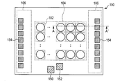
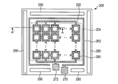
- 2A and 2B are views showing an example of a planar layout of the readout circuit board and the sensor board constituting the imaging apparatus according to the present embodiment.
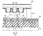
- FIG. 3 is a schematic cross-sectional view showing the structure of the imaging apparatus according to the present embodiment.
- FIG. 4 is a schematic cross-sectional view showing the structure of the sensor substrate constituting the imaging apparatus according to the present embodiment.
- FIG. 5 is a view for explaining the optical connection between the readout circuit board and the sensor board constituting the imaging apparatus according to the present embodiment.
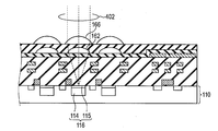
- FIG. 6 is a diagram for explaining a locus of light passing through an optical system of a general CMOS image sensor used in a visible light band camera or the like.
- FIG. 7 is an equivalent circuit diagram for explaining the operation of the sensor substrate constituting the imaging apparatus according to the present embodiment.
- the image pickup apparatus 300 has a structure in which a readout circuit board 100 and a sensor board 200 are bonded together as shown in FIG.
- the sensor substrate 200 is a substrate including an optical sensor for imaging.
- the readout circuit board 100 is a board including a readout integrated circuit (RoIC: Readout Integrated Circuit) for outputting information detected by the optical sensor of the sensor substrate 200 as a readout image signal.
- the readout circuit board 100 and the sensor board 200 are bonded together with a spacer 290 so as to face each other with a predetermined gap.
- Bumps 170 are provided between the readout circuit board 100 and the sensor board 200 and serve to electrically connect them.
- a silicon substrate accumulated in wafer process technology and integration technology is preferably used from the viewpoint of providing readout integrated circuits.
- the main reason for mounting the optical sensor on the sensor substrate 200 different from the readout circuit substrate 100 is to use a substrate having a light absorption characteristic different from that of the constituent material of the readout circuit substrate 100.
- a substrate made of a material different from silicon such as a compound semiconductor substrate, is preferably used as the base material of the sensor substrate 200.
- the compound semiconductor substrate include an InP substrate and a GaAs substrate.
- the absorption wavelength band of materials such as InGaAs, GaAsSb, and AlGaInAsP that can grow crystals on InP and GaAs substrates is longer than the absorption wavelength band of single crystal silicon.
- the sensor substrate 200 may be a substrate in which a compound semiconductor layer such as an InP layer is provided on another substrate such as a sapphire substrate.
- a silicon substrate is used as the base material of the readout circuit substrate 100 and an InP substrate is used as the base material of the sensor substrate 200 will be described.
- the materials of the readout circuit substrate 100 and the sensor substrate 200 are as necessary. It can be selected appropriately.
- FIG. 2A is a diagram illustrating an example of a planar layout of the read circuit board 100.
- the readout circuit substrate 100 includes a pixel region 104 in which a plurality of pixels 102 are arranged in a matrix, and a peripheral circuit for executing driving of the pixels 102 and processing of output signals of the pixels 102.
- a peripheral circuit region 106 is provided.
- the readout circuit board 100 also includes pad electrodes 150 and 152 for electrical connection with the sensor substrate 200 via the bumps 170 and a plurality of pad electrodes 154 for electrical connection with the outside. Is provided.
- the pad electrodes 150 and 152 are provided outside the pixel region 104.
- the pad electrodes 150 and 152 are connected to a peripheral circuit via an internal wiring (not shown) so that power can be supplied to the sensor substrate 200 via the pad electrodes 150 and 152 and the bump 170.
- FIG. 2B is a diagram illustrating an example of a planar layout of the sensor substrate 200.
- the sensor substrate 200 is provided with a pixel region 204 in which a plurality of pixels 202 are arranged in a matrix and a spacer 290 that is arranged so as to surround the pixel region 204.
- the sensor substrate 200 also includes a pad electrode 270 electrically connected to a common electrode 262 disposed so as to surround the pixel region 204, and a pad electrode 272 electrically connected to the ring electrode 260 of each pixel 202. And are provided.
- the pad electrodes 270 and 272 are provided outside the pixel region 204.
- the plurality of pixels 202 are arranged so as to face the plurality of pixels 102 arranged in the pixel region 104 of the readout circuit substrate 100 when the readout circuit substrate 100 and the sensor substrate 200 are bonded to each other.
- the pad electrodes 270 and 272 are disposed so as to face the pad electrodes 150 and 152 disposed on the read circuit board 100 when the read circuit board 100 and the sensor substrate 200 are bonded to each other.
- FIG. 3 is a schematic cross-sectional view taken along the line AA ′ in FIGS. 2A and 2B after the read circuit board 100 and the sensor board 200 are bonded together.
- the read circuit board 100 includes a silicon substrate 110 as a base material.
- the pixel region 104 and the peripheral circuit region 106 described above are provided on the silicon substrate 110.
- FIG. 3 shows three pixels 102 arranged in the pixel region 104 and one peripheral transistor MP arranged in the peripheral circuit region 106. Actually, a plurality of pixels 102 are arranged in a matrix in the pixel region 104.
- the peripheral circuit region 106 is provided with a plurality of peripheral transistors MP including those of the reverse conductivity type.
- the signal charge is an electron will be described as an example, but the signal charge may be a hole.
- the conductivity type of each semiconductor region is a reverse conductivity type.
- Each pixel 102 includes a light receiving unit 116, a floating diffusion (hereinafter referred to as “FD”), a transfer transistor M 1, a first lens 162, and a second lens 166.
- FD floating diffusion
- the pixel 102 may have an in-pixel readout circuit including an amplification transistor, a reset transistor, a selection transistor, and the like, as in a general CMOS image sensor.
- the light receiving unit 116 is a photodiode including an n-type semiconductor region 114 and a p-type semiconductor region 115 provided in the silicon substrate 110. Signal charges generated by photoelectric conversion in the silicon substrate 110 are collected in the n-type semiconductor region 114. The p-type semiconductor region 115 is arranged so as to contact the main surface 112 of the silicon substrate 110.
- the photodiode constituting the light receiving unit 116 is a so-called embedded photodiode.
- the FD is configured by an n-type semiconductor region 118 provided in the silicon substrate 110.
- the transfer transistor M1 includes a gate electrode 128 provided on the silicon substrate 110 between the n-type semiconductor region 114 and the n-type semiconductor region 118 with a gate insulating film 124 interposed therebetween.
- the transfer transistor M1 has a function of transferring the signal charge generated by the light receiving unit 116 and accumulated in the n-type semiconductor region 114 to the FD.
- the signal charge transferred to the FD is converted into a voltage corresponding to the amount of the signal charge transferred from the light receiving unit 116 by the capacitance component of the FD.
- the FD is electrically connected to an input node of an amplifying unit (not shown).
- the amplifying unit may be disposed in each pixel.
- the FD is electrically connected to a signal output line (not shown).
- the peripheral transistor MP includes n-type semiconductor regions 120 and 122 as source / drain regions provided in the silicon substrate 110, and a silicon substrate 110 between the n-type semiconductor regions 120 and 122 via a gate insulating film 126. And a provided gate electrode 130.
- An insulating layer 140 is provided on the silicon substrate 110.
- the insulating layer 140 can be made of, for example, silicon oxide.
- a first wiring layer 142 and a second wiring layer 144 are provided in the insulating layer 140.
- a third wiring layer 146 is provided on the insulating layer 140.
- the first wiring layer 142, the second wiring layer 144, and the third wiring layer 146 are arranged at different heights with the main surface 112 of the silicon substrate 110 as a reference.
- the first wiring layer 142 and the second wiring layer 144 are made of a conductive member mainly composed of copper, for example.
- the third wiring layer 146 is made of a conductive member mainly composed of aluminum, for example.
- the pad electrodes 150, 152, and 154 are configured by the third wiring layer 146.
- a part of the conductive members of the first wiring layer 142 and a part of the conductive members of the second wiring layer 144 are electrically connected by a via plug (not shown).
- a part of the conductive member of the second wiring layer 144 and a part of the conductive member of the third wiring layer 146 are electrically connected by a via plug (not shown).
- the via plug can be made of a conductive material such as tungsten.
- the conductive member of the first wiring layer 142, the conductive member of the second wiring layer 144, and the conductive member of the third wiring layer 146 are insulated from each other by the insulating layer 140 except for a portion that is electrically connected by a via plug. .
- the third wiring layer 146 among the plurality of wiring layers is assumed to be the wiring layer arranged farthest from the silicon substrate 110.
- the insulating layer 140 does not necessarily need to be made of one type of insulating material, and may be made of a laminate of a plurality of insulating layers containing different materials.
- the insulating layer 140 may include an antireflection film that prevents reflection on the surface of the silicon substrate 110, a diffusion prevention film that prevents diffusion of the conductive member, an etching stopper film, and the like.
- the number of wiring layers is not limited to three.
- the conductive members constituting the first wiring layer 142, the second wiring layer 144, and the third wiring layer 146 are not limited to the above example.
- the first wiring layer 142 and the second wiring layer 144 are not included.
- the conductive member may be mainly composed of aluminum.
- An insulating layer 160 is provided on the insulating layer 140 provided with the third wiring layer 146.
- the insulating layer 160 can function as a protective film.
- a first lens 162 is disposed on the insulating layer 160 corresponding to each pixel 102.
- the insulating layer 160 and the first lens 162 can be made of, for example, silicon nitride.
- the refractive index of the constituent member of the insulating layer 160 and the constituent member of the first lens 162 are both higher than the refractive index of the constituent member of the insulating layer 140.
- the refractive index of the constituent member of the insulating layer 160 may be different from the refractive index of the constituent member of the insulating layer 140.
- the insulating layer 160 and the first lens 162 are not necessarily provided.
- a planarization film 164 and a second lens 166 may be further provided on the first lens 162.
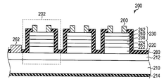
- the sensor substrate 200 includes an InP substrate 210 as a base material.
- the aforementioned pixel region 204 is provided on the InP substrate 210.
- a common layer 212 made of, for example, p-type InP is provided on the InP substrate 210.
- a plurality of pixels 202 made of a mesa structure including a light receiving unit 220, a light emitting unit 230, and a ring electrode 260 are provided.
- the common layer 212 may be a part of a semiconductor layer constituting the light receiving unit 220.
- a protective film 280 is provided on the side wall of the mesa structure.
- An antireflection film 214 is provided on the back surface of the InP substrate 210.
- the ring electrode 260 and the pad electrode 272 of the plurality of pixels 202 constituting the pixel region 204 are electrically connected to each other as shown in FIG. 2B.
- the light receiving portions 220 of the plurality of pixels 202 constituting the pixel region 204 are connected to the common layer 212.
- it is electrically connected to the pad electrode 270 via a common electrode 262 for making electrical contact with the common layer 212.
- the mesa structure of the plurality of pixels 202 is designed to be applied with substantially the same voltage through the ring electrode 260 and the common electrode 262.
- the layer configuration shown in FIG. 4 can be applied. Note that FIG. 4 is upside down from FIG. 3 because each layer is described in the order of crystal growth on the InP substrate 210.
- a common layer 212 connected to the light receiving unit 220 of each pixel 202 is provided on the main surface of the InP substrate 210 having a thickness of about 500 ⁇ m.
- the common layer 212 is made of p-type InP having a thickness of 3 ⁇ m, for example.
- an undoped InGaAs layer 222 having a thickness of 4 ⁇ m and an n-type InP layer 224 having a thickness of 1 ⁇ m are stacked in this order.
- the common layer 212, the undoped InGaAs layer 222, and the n-type InP layer 224 constitute the light receiving unit 220 described above, and the undoped InGaAs layer 222 functions as a light receiving layer.
- the light receiving layer made of InGaAs has an absorption wavelength band in the infrared wavelength band.
- an n-type InP layer 232 having a thickness of 4 ⁇ m, an undoped InP layer 234, and a p-type InP layer 236 are stacked in this order.
- the n-type InP layer 232, the undoped InP layer 234, and the p-type InP layer 236 constitute the light emitting unit 230 described above, and the undoped InP layer 234 functions as a light emitting layer.
- the emission center wavelength of the light emitting unit 230 having the light emitting layer made of InP is about 920 nm.
- a ring electrode 260 is provided on the p-type InP layer 236 via an InGaAs contact layer (not shown). As described above, the ring electrodes 260 provided on the light emitting units 230 of the respective pixels 202 are electrically connected to each other, and substantially eliminate the voltage drop due to the electrical resistance of the wiring connecting them. Are at the same potential.
- the readout circuit board 100 and the sensor board 200 are arranged so that their main surfaces are opposed and parallel to each other.
- the plurality of pixels 102 of the readout circuit substrate 100 and the plurality of pixels 202 of the sensor substrate 200 are arranged at the same pitch so as to be paired with each other.
- the light receiving unit 116 of the pixel 102 and the light emitting unit 230 of the pixel 202 are optically connected via the first lens 162 and the second lens 166.
- the imaging apparatus includes the light emitting unit 230 on the sensor substrate 200 provided with the imaging sensor element (the light receiving unit 220), and the light receiving unit 116 on the readout circuit board 100 provided with the RoIC. have. Then, the light emitted from the light emitting unit 230 provided on the sensor substrate 200 is detected by the light receiving unit 116 provided on the reading circuit substrate 100. For this reason, the light emitting unit 230 emits light according to the amount of light received by the light receiving unit 220 and is detected by the light receiving unit 116, whereby the information detected by the light receiving unit 220 can be read and sent to the circuit board 100. . That is, in the imaging apparatus according to the present embodiment, the pixel 102 provided on the readout circuit substrate 100 and the pixel 202 provided on the sensor substrate 200 are not electrically connected via metal bumps.
- FIG. 5 is a diagram for explaining optical connection between the readout circuit board 100 and the sensor board 200.
- the first lens 162 and the second lens 166 constitute one lens group, and the light 400 emitted from the light emitting unit 230 of the sensor substrate 200 is read out by the lens group. 100 images are formed on the light receiving unit 116.
- an optical system is designed based on the relationship of the following formula (1) based on a so-called lens formula.
- 1 / f 1 / d 1 + 1 / d 2
- d 1 is an optical distance from the interface between the second lens 166 and air to the light receiving unit 116.
- d 2 is an optical distance from the interface between the second lens 166 and air to the light emitting unit 230.
- f is an effective focal length of the lens group.
- the optical distance is represented as the product of the refractive index of a substance through which light propagates and the physical distance through which light propagates.
- FIG. 6 shows an example of a trajectory of light 402 that passes through an optical system of a general CMOS image sensor used in a camera having sensitivity in the visible light band.
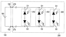
- FIG. 7 is an equivalent circuit diagram for explaining the operation of the sensor substrate 200.
- the photodiode D1 corresponds to the light receiving unit 220 in FIG. 3
- the light emitting diode D2 corresponds to the light emitting unit 230 in FIG. Note that in FIG. 7, wirings that connect the ring electrodes 260 of each pixel 202, and the electrical resistances of the common electrode 262 and the common layer 212 are omitted.
- the photodiode D1 and the light emitting diode D2 constituting each pixel 202 are connected in series so that the directions of the pn junctions are opposite to each other.
- the DC power supply 180 supplied from the readout circuit board 100 to the sensor board 200 via the pad electrodes 150, 152, 270, and 272 applies a reverse bias to the photodiode D1 and applies a forward bias to the light emitting diode D2.
- the voltage of the DC power supply 180 is, for example, 5.0V.
- the DC power supply 180 When the DC power supply 180 is connected to the series connection body of the photodiode D1 and the light emitting diode D2 in this way, most of the voltage supplied from the DC power supply 180 is applied to the photodiode D1. As a result, the photodiode D1 is in a state where a sufficient reverse bias is applied, and the current flowing through the photodiode D1 changes depending on the amount of light incident on the photodiode D1. Since the photodiode D1 and the light emitting diode D2 are connected in series, the current flowing through the light emitting diode D2 is the same as the current flowing through the photodiode D1.
- the amount of light emitted from the light emitting diode D2 is proportional to the value of the current flowing through the light emitting diode D2, not the voltage applied to the light emitting diode D2, as in a general LED. As a result, the light emitting diode D2 emits light with a light amount proportional to the amount of light incident on the photodiode D1.
- a certain amount of light is fed back from the light emitting unit 230 to the light receiving unit 220 due to its structure.
- the feedback amount exceeds 1 and becomes positive feedback
- the light emitting unit 230 exceeds the threshold value
- the light emitting unit 230 emits light regardless of the amount of light incident on the light receiving unit 220, and the information of the light receiving unit 220 is read out. Cannot send to 100. Therefore, the amount of feedback from the light emitting unit 230 to the light receiving unit 220, more specifically, the amount of current flowing into the light emitting unit 230 is generated by the light receiving unit 220 by the light emitted from the light emitting unit 230 by the current. A small amount of current is required. Therefore, for example, a configuration as described in Patent Document 2 that has two stable states due to positive feedback and has an effect as a memory is unsuitable as a configuration of the sensor substrate 200 of the imaging apparatus according to the present embodiment.
- the laminated body from the common layer 212 to the p-type InP layer 236 has a pnp structure as a whole although an i layer is inserted in the middle. Therefore, when the total film thickness of the n-type InP layers 224 and 232 is equal to or less than the thickness at which holes which are minority carriers can be diffused, an operation like a bipolar transistor is exhibited. When the operation like a bipolar transistor becomes remarkable and the amplification effect exceeds a certain level, positive feedback occurs from the light emitting unit 230 to the light receiving unit 220, and the amount of light emitted by the light emitting unit 230 corresponds to the amount of light received by the light receiving unit 220. It will not become.
- the total film thickness of the n-type InP layers 224 and 232 corresponding to the base layer corresponds to the diffusion length of minority carriers. It is made thicker than the thickness.
- the hole diffusion length in the n-type InP layers 224 and 232 of this embodiment is about 4 ⁇ m. Therefore, in this embodiment, the total film thickness of the n-type InP layers 224 and 232 is set to 5 ⁇ m, which is thicker than the hole diffusion length.
- the hole diffusion length is about 4 ⁇ m, but the hole diffusion length varies depending on the material and the like, and the amplification factor of the bipolar transistor is the doping of each layer constituting the pn junction. Varies with concentration. Therefore, it is desirable that the total film thickness of the n-type layer is appropriately adjusted according to the constituent materials of the light receiving unit 220 and the light emitting unit 230 and the doping concentration of each layer.
- minority carrier diffusion is blocked by inserting a layer having a larger energy band gap than the surroundings, such as AlInP, into the stacked body constituting the light receiving unit 220 and the light emitting unit 230 and providing a barrier on the valence band side. You may do it. Further, in order to confine minority carriers, a layer having a smaller energy band gap than InP may be inserted to promote carrier accumulation and recombination.
- a layer having a larger energy band gap than the surroundings such as AlInP
- the thickness of the InP substrate 210 is about 500 ⁇ m, and the thickness is not greatly reduced from the initial thickness of the InP substrate 210 used for crystal growth of each layer. In addition to facilitating handling during the manufacture of the sensor substrate 200, this has the purpose of absorbing visible light.
- an InP substrate 210 with a thickness of about 230 ⁇ m is required to absorb 99% of light with a wavelength of 950 nm. Since the absorption coefficient of light on the shorter wavelength side than the wavelength of 950 nm is even greater, visible light can be reliably absorbed with a thickness of about 230 ⁇ m or more.
- the read circuit board 100 and the sensor board 200 are respectively formed by a semiconductor wafer process. Thereafter, metal bumps made of a metal material such as gold or copper are formed on the pad electrodes 150 and 152 of the readout circuit substrate 100 and the pad electrodes 270 and 272 of the sensor substrate 200, respectively.
- the sensor board 200 is positioned and installed on the readout circuit board 100, and the sensor board 200 is pressed against the readout circuit board 100 at an elevated temperature.
- the metal bumps placed on the pad electrodes 150 and 152 and the metal bumps placed on the pad electrodes 270 and 272 are thermocompression bonded, respectively, and electrical connection between the readout circuit board 100 and the sensor board 200 is established.
- the distance between the readout circuit board 100 and the sensor board 200 is defined by the height of the spacer 290.
- the electrical connection between the readout circuit board 100 and the sensor board 200 is only the bump 170 that connects between the pad electrode 150 and the pad electrode 270 and between the pad electrode 152 and the pad electrode 272. is there. Therefore, the influence of the bonding process between the readout circuit board 100 and the sensor board 200 on the manufacturing yield can be reduced, and the connection reliability between the readout circuit board 100 and the sensor board 200 can be improved.
- an adhesive is applied to the outer periphery of the sensor substrate 200 using a dispenser or the like, and the sensor substrate 200 is fixed to the readout circuit substrate 100.
- the number and arrangement of pad electrodes for electrically connecting the readout circuit substrate 100 and the sensor substrate 200, the outer peripheral shape of the pixel regions 104 and 204, the arrangement of the peripheral circuit region 106, and the like are changed as necessary. can do.
- the electrical connection method between the readout circuit board 100 and the sensor board 200 is not limited to the metal bumps as long as it can supply power, and for example, a conductive paste or the like may be used.
- the method for fixing the sensor substrate 200 to the readout circuit substrate 100 is not limited to the adhesive, and other fixing methods may be used.
- image information captured by the sensor substrate 200 can be transmitted to the readout circuit board 100 and electrically read out without using electrical connection for each pixel. This makes it easy to reduce the pixel size and increase the area of the sensor unit, and to realize a high-performance and highly reliable imaging apparatus that can acquire an image in a long wavelength band exceeding 1.0 ⁇ m. it can.
- FIG. 8 is a schematic cross-sectional view showing the structure of the sensor substrate constituting the imaging apparatus according to the present embodiment.
- the imaging device according to the present embodiment is the same as the imaging device according to the first embodiment, except that the configuration of the light emitting unit 230 provided on the sensor substrate 200 is different. That is, in the pixel 202 of the imaging apparatus according to the present embodiment, as shown in FIG. 8, the n-type AlInAs layer 238, the undoped AlGaInAs layer 240, and the p-type AlInAs layer 242 are arranged in this order on the light receiving unit 220.
- the light emitting unit 230 is stacked.
- the undoped AlGaInAs layer 240 functions as a light emitting layer.
- AlGaInAs constituting the undoped AlGaInAs layer 240 is a mixed crystal of AlAs, GaAs, and InAs, and the energy band gap, that is, the emission center wavelength can be controlled in accordance with the composition ratio. Accordingly, a composition having a larger energy band gap than InP used in the light emitting layer of the light emitting unit 230 in the imaging device of the first embodiment can be realized.
- the emission center wavelength can be set to about 820 nm.
- the sensitivity of the photodiode made of silicon (the light receiving unit 116) is higher for light having a wavelength of 820 nm than light having a wavelength of 920 nm, which is the emission center wavelength of InP, and thus the light emission of the light emitting unit 230 is higher. It becomes possible to detect with sensitivity.
- the light emitting layer of the light emitting unit 230 is made of AlGaInAs, but any material that has a desired emission center wavelength and can be epitaxially grown on the base material (InP substrate 210) is particularly suitable. It is not limited. For example, AlInAs excluding Ga may be used instead of AlGaInAs.
- the light emitting layer may be composed of a plurality of layers or may have a quantum well structure.
- a structure used in a general LED can be introduced.
- FIG. 9 is a schematic cross-sectional view showing the structure of the sensor substrate constituting the imaging apparatus according to the present embodiment.
- the imaging device according to the present embodiment is the same as the imaging device according to the first and second embodiments, except that the configuration of the light emitting unit 230 provided on the sensor substrate 200 is different. That is, the pixel 202 of the imaging apparatus according to the present embodiment includes an n-type AlInAs layer 238, an undoped AlGaInAs layer 240, and an undoped AlInAs layer 244 stacked in this order on the light receiving unit 220, as shown in FIG.
- the light emitting unit 230 is formed.
- the undoped AlInAs layer 244 is provided with p-type regions 250 and 252.
- the p-type region 250 is provided on the surface portion of the undoped AlInAs layer 244 so as to be in contact with the ring electrode 260.
- the p-type region 252 is provided in the undoped AlInAs layer 244 inside the ring electrode 260 from the surface portion of the undoped AlInAs layer 244 to a depth greater than the depth of the p-type region 250. In this way, an in-plane distribution is provided for the p-type impurity added to the undoped AlInAs layer 244.
- the current flowing through the light emitting unit 230 is concentrated on the path passing through the p-type region 252 where the width in the depth direction of the undoped AlInAs layer 244 is the narrowest, and the region emits strong light locally.
- the ratio of light emission in the light extraction window region inside the ring electrode 260 can be increased, and the light extraction efficiency can be improved.
- the p-type regions 250 and 252 are not particularly limited.
- the p-type regions 250 and 252 can be formed by adding Zn to the undoped AlGaInAs layer 240 by an ion implantation method.
- the p-type regions 250 and 252 having different depths can be formed by changing the acceleration energy of the implanted ions.
- the application example to the imaging apparatus according to the second embodiment has been described.
- the same configuration may be applied to the imaging apparatus according to the first embodiment.
- the p-type InP layer 236 may be an undoped InP layer, and a p-type region similar to the p-type regions 250 and 252 may be provided in the undoped InP layer.
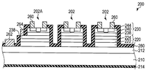
- FIG. 10 is a schematic cross-sectional view showing the structure of the sensor substrate constituting the imaging apparatus according to the present embodiment.
- the imaging apparatus according to the present embodiment is the first in that a part of the plurality of pixels 202 provided on the sensor substrate 200 further includes an individual electrode connected to the n-side terminal of the light emitting unit 230.
- the imaging device according to the third embodiment is different.
- FIG. 10 shows an example in which the above configuration of the present embodiment is applied to the sensor substrate 200 of the imaging apparatus according to the third embodiment. That is, some of the pixels 202A among the plurality of pixels 202 provided on the sensor substrate 200 have the individual electrodes 264 provided on the n-type AlInAs layer 238 which is the n-side terminal of the light emitting unit 230. Yes. Similar to the ring electrode 260 and the common electrode 262, the individual electrode 264 is electrically connected to a peripheral circuit provided on the readout circuit board 100 through wiring and bumps (not shown).
- the light emitting unit 230 of the pixel 202A applies a voltage between the individual electrode 264 as the n-side electrode and the ring electrode 260 as the p-side electrode, so that the light is not incident on the light receiving unit 220.
- the light can be emitted independently.
- the light emitting unit 230 provided in the pixel 202A can be used not only to transmit information to the pixel 102 but also to confirm alignment between the readout circuit board 100 and the sensor board 200. For example, after the readout circuit substrate 100 and the sensor substrate 200 are joined, a voltage is applied between the individual electrode 264 and the ring electrode 260 to cause the light emitting unit 230 of the pixel 202A to emit light, and the pixel 102 that makes a pair with the pixel 202A. The amount of light received by the light receiving unit 116 is confirmed. By doing in this way, it can be checked whether the position shift of the joining in the direction parallel to the main surface of the substrate is within an allowable range. As a result, it is possible to prevent defective products whose positional deviation between the readout circuit board 100 and the sensor board 200 is outside the allowable range from being sent to the mounting process on the ceramic package.
- the arrangement location and the number of the pixels 202A in the pixel area 204 are not particularly limited. From the viewpoint of detecting a two-dimensional misalignment between the readout circuit board 100 and the sensor board 200, at least two pixels 202A arranged at remote locations are necessary. For example, when the pixel region 204 has a rectangular shape as shown in FIG. 2B, two to four pixels 202 positioned in the vicinity of the four corners of the pixel region 204 can be used as the pixel 202A.
- the confirmation of the amount of misalignment between the readout circuit board 100 and the sensor board 200 may be performed when the readout circuit board 100 and the sensor board 200 are joined.
- the light emitting portion 230 of the pixel 202A emits light, and an optimal location is monitored while monitoring the amount of light received by the light receiving portion 116 of the pixel 102 paired with the pixel 202A. Align to.
- ⁇ An effect in this case is that alignment can be performed with higher accuracy than the mechanical alignment accuracy of the mounting device.
- the lens is used for optical connection between the light emitting unit 230 of the sensor substrate 200 and the light receiving unit 116 of the readout circuit substrate 100, or when the pixel pitch is 10 micrometers or less.
- Great effect when small is very when the lens is loaded is that the amount of fluctuation in the amount of light when there is a shift between the region and the light receiving unit 116 because the light is focused on a small region by the lens is not present. It is because it becomes large compared with.
- a pattern on the readout circuit board 100 and a pattern on the sensor board 200 are recognized by image recognition, and a positional deviation amount in a direction parallel to the main surface is grasped. Thereafter, the readout circuit board 100 and the sensor board 200 are brought close to each other and heated to bond the bumps.
- misalignment occurs not a little, such as misalignment from the ideal position.
- the pixel pitch is relatively large, the problem due to the shift is small, but when the pixel pitch approaches a normal visible light band image sensor made of silicon, the influence of the alignment shift cannot be ignored.
- the reading circuit board 100 and the sensor board 200 are brought close to a few micrometers before contact, and the light emitting unit 230 of the pixel 202A is caused to emit light in that state, and the light receiving unit 116 monitors the received light amount to maximize the amount of received light. Find a location. By doing so, the alignment can be performed in a state where the readout circuit board 100 and the sensor board 200 are as close as possible without using image recognition, so that the displacement due to the movement after the alignment or the like can be greatly reduced.
- the application example to the imaging apparatus according to the third embodiment has been described.
- the same configuration may be applied to the imaging apparatus according to the first or second embodiment.
- the alignment accuracy between the readout circuit board 100 and the sensor board 200 can be improved. Thereby, an improvement in manufacturing yield and further enhancement of sensitivity can be realized.
- FIG. 11 is a schematic cross-sectional view illustrating the structure of the imaging apparatus according to the present embodiment.
- the imaging device according to the present embodiment is different from the imaging devices according to the first to fourth embodiments in that it further includes a lens 282 provided on the light emitting unit 230 of the sensor substrate 200. Yes.
- the lens 282 has a function of shaping light emitted from the light emitting unit 230 into substantially parallel light.
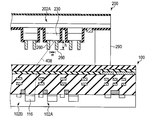
- the first lens 162 and the second lens 166 provided on the readout circuit board 100 are configured to collect the parallel light 404 emitted from the lens 282 on the light receiving unit 116. Yes.
- the imaging apparatus since the lens 282 is also provided on the sensor substrate 200 side, the number of manufacturing steps increases. However, the imaging apparatus according to the present embodiment has a unique effect that fluctuations in optical coupling efficiency due to variations in the distance between the readout circuit board 100 and the sensor board 200 can be suppressed.
- In-plane distribution or variation may occur in the interval between the readout circuit substrate 100 and the sensor substrate 200 due to warpage of the readout circuit substrate 100 and the sensor substrate 200 or variations in the bonding process.
- the distance between the readout circuit board 100 and the sensor board 200 changes, the distance between the lens group constituted by the first lens 162 and the second lens 166 and the light emitting unit 230 changes.
- a shift occurs between the position where the light beam is collected by the lens group and the position of the surface of the light receiving unit 116, and the optical coupling between the readout circuit board 100 and the sensor board 200. The efficiency will be affected.
- the light emitted from the light emitting unit 230 is shaped into the parallel light 404 by the lens 282, so that the light is collected in the readout circuit board 100 even if the distance between the boards changes.
- the position where the light shines hardly changes.
- the variation in the optical coupling efficiency due to the in-plane distribution and the variation in the distance between the readout circuit substrate 100 and the sensor substrate 200 can be reduced. Can be suppressed.
- FIG. 12 is a schematic cross-sectional view showing the structure of the imaging apparatus according to the present embodiment.
- FIG. 13 is a graph showing the relationship between the distance between the readout circuit board and the sensor board and the optical coupling efficiency.
- the imaging apparatus according to the present embodiment is the same as the imaging apparatus according to the first to fourth embodiments, except that the lens group (the first lens 162 and the second lens 166) is not provided on the readout circuit board 100.
- the lens group the first lens 162 and the second lens 166
- a lens group is not necessarily provided in the optical connection between the light emitting unit 230 of the pixel 202 provided on the sensor substrate 200 and the light receiving unit 116 of the pixel 102 provided on the readout circuit substrate 100, as shown in this embodiment.
- a lens group is not necessarily provided. There is no need to use.
- the imaging apparatus according to the present embodiment has an advantage that the manufacturing cost can be reduced by omitting the step of forming the first lens 162 and the second lens 166.
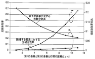
- FIG. 13 is a graph showing the results of calculating the inter-substrate distance dependency of the optical coupling efficiency between the readout circuit substrate 100 and the sensor substrate 200 in the configuration of the imaging apparatus according to the present embodiment.
- the horizontal axis represents the optical distance L (see FIG. 12) between the surface position of the light emitting unit 230 and the surface position of the light receiving unit 116.
- the left vertical axis represents the optical coupling efficiency between the pixel 202 and the pixel 102.
- the right vertical axis represents the ratio between the optical coupling efficiency to the pixel 102 immediately below and the optical coupling efficiency to the pixel 102 adjacent to the pixel 102 immediately below.
- the plots marked with ⁇ indicate the optical coupling efficiency between the pixel 202 and the pixel 102 immediately below the pixel 202.
- the plot with (2) indicates the optical coupling efficiency between the pixel 202 and the pixel 102 adjacent to the pixel 102 immediately below the pixel 202.
- the plots with ⁇ indicate the ratio between the optical coupling efficiency to the pixel 102 immediately below and the optical coupling efficiency to the adjacent pixel 102.
- the optical coupling efficiency between the pixel 202 and the pixel 102 increases as the distance between the readout circuit substrate 100 and the sensor substrate 200 is reduced. Therefore, by appropriately setting the interval between the readout circuit board 100 and the sensor board 200 according to the required optical coupling efficiency, desired characteristics can be realized even in a configuration in which no lens group is provided on the readout circuit board 100. It is possible to do.
- the amount of light incident on the light receiving unit 116 of the pixel 102 directly below the light receiving unit 116 of the adjacent pixel 102 can be suppressed to about 3.5% or less.
- an imaging device that detects light in a wavelength band exceeding 1.0 ⁇ m is a so-called monochrome imaging device that does not have filters with different transmission wavelength bands depending on pixels. is there. Therefore, depending on the application, it may be usable even if the crosstalk to adjacent pixels is about 3.5%.
- an imaging apparatus can be realized at a lower cost by a configuration in which a lens is not provided as in the present embodiment. Further, if the crosstalk to the adjacent pixels can be allowed to about 10%, the distance L between the readout circuit board 100 and the sensor board 200 can be increased to about 7 ⁇ m.
- the application example to the imaging device according to the first to fourth embodiments has been described, but the same configuration as that of this embodiment may be applied to the imaging device according to the fifth embodiment.
- the manufacturing cost can be reduced.
- FIG. 14 is a schematic cross-sectional view illustrating the structure of the imaging apparatus according to the present embodiment.
- a light shielding wall for example, a ring electrode 260 can be used.
- the ring electrode 260 is used as a light shielding wall in the imaging apparatus according to the sixth embodiment.
- the area inside the ring electrode 260 of the light emitting unit 230 is an opening through which light is emitted.
- a ring electrode 260 having a height higher than that in the first to sixth embodiments is assumed, and a case where light emitted from the light emitting unit 230 can be transmitted through the ring electrode 260 is considered.
- the light rays that pass through the highest portion of the ring electrode 260 are dotted lines in FIG.
- the ring electrode 260 when the ring electrode 260 is used as a light shielding wall, when the height h of the ring electrode 260 (light shielding wall) satisfies the relationship of the following expression (3), the light receiving unit 116 of the pixel 102B adjacent to the pixel 102A immediately below. It is possible to effectively block light incident on the. h> w ⁇ tan ⁇ 1 (3)
- ⁇ 1 is an angle formed by the light beam 408 with respect to the surface of the light emitting unit 230
- w is the width of the opening of the light emitting unit 230 (see FIG. 14).
- the width w of the opening of the light emitting unit 230 is 5 ⁇ m
- the width of the opening of the light receiving unit 116 is 5 ⁇ m
- the optical distance between the surface of the light emitting unit 230 and the surface of the light receiving unit 116 is 5 ⁇ m
- the pixel pitch is 19 ⁇ m.
- the height h of the oblique light wall satisfying the above relationship is 1.3 ⁇ m.
- the difference between the height of the oblique light wall and the height from the light emission surface of the light emitting unit 230 is important. Therefore, it is not always necessary to provide a member as an oblique light wall up to its height.
- an oblique light wall having the same effect can be realized by etching a portion of the light emitting portion 230 that emits light by 0.5 ⁇ m and arranging a ring electrode 260 having a height of 0.8 ⁇ m around the etched portion. it can.
- the light shielding wall satisfying the expression (3) is not necessarily the ring electrode 260, and may be formed using another member. Further, a light shielding wall having a similar function may be provided on the readout circuit board 100 side.
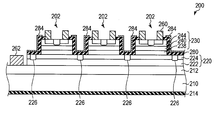
- FIG. 15 is a schematic cross-sectional view showing the structure of the sensor substrate that constitutes the imaging apparatus according to the present embodiment.
- each pixel 202 provided on the sensor substrate 200 is formed of a mesa structure including a light receiving unit 220 and a light emitting unit 230.
- the light emitting unit 230 has an independent mesa structure for each pixel 202, but the undoped InGaAs layer 222 and n that constitute the light receiving unit 220.
- the type InP layer 224 is not patterned for each pixel 202.
- a p-type region 226 is provided in a region between the pixels 202 of the n-type InP layer 224.
- the p-type region 226 is formed so as to surround the periphery of each pixel 202 in plan view.
- the p-type region 226 is not particularly limited.
- the p-type region 226 can be formed by adding Zn to the n-type InP layer 224 by an ion implantation method.
- a pn junction can be formed at the interface between the n-type InP layer 224 and the p-type region 226. Due to the reverse characteristics of the pn junction, the light receiving portions 220 of the adjacent pixels 202 can be electrically separated.
- the etching depth when forming the mesa structure is smaller than in the case of the first to seventh embodiments in which the mesa structure including the light receiving unit 220 and the light emitting unit 230 is formed. Therefore, the machining process can be facilitated. Further, since the light receiving unit 220 does not have a mesa structure, no surface current flows through the mesa side wall.
- the imaging apparatus further includes a light shielding film 284 between the light emitting units 230 of the adjacent pixels 202.
- the light-shielding film 284 is not particularly limited, but can be constituted by a laminated film of a Cr film having a thickness of 10 nm and an Au film having a thickness of 100 nm, for example.
- the reason why the light shielding film 284 is provided in the imaging apparatus according to the present embodiment is to prevent light generated by the light emitting unit 230 of a certain pixel 202 from entering the light receiving unit 220 (undoped InGaAs layer 222) of the adjacent pixel 202. It is. Thereby, crosstalk of light between the pixels 202 can be suppressed.
- the light shielding film 284 is also applicable to the imaging devices according to the first to seventh embodiments. However, in the imaging device according to the first to seventh embodiments, as described above, since the depth of the groove necessary for separating the mesa structure of each pixel 202 is deeper than that in the present embodiment, the light shielding film The relative difficulty of forming 284 increases.
- the application example to the imaging apparatus according to the third embodiment has been described.
- the same configuration as that of the present embodiment may be applied to imaging apparatuses according to other embodiments.
- the manufacturing process can be facilitated and crosstalk to adjacent pixels can be reduced.
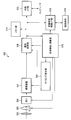
- FIG. 16 is a block diagram illustrating a schematic configuration of the imaging system according to the present embodiment.
- the imaging apparatus 300 described in the first to eighth embodiments can be applied to various imaging systems.
- Examples of applicable imaging systems include digital still cameras, digital camcorders, surveillance cameras, copiers, fax machines, mobile phones, in-vehicle cameras, observation satellites, and the like.
- a camera module including an optical system such as a lens and an imaging device is also included in the imaging system.
- FIG. 16 illustrates a block diagram of a digital still camera as an example of these.
- An imaging system 500 illustrated in FIG. 16 protects the imaging device 501, a lens 502 that forms an optical image of a subject on the imaging device 501, a diaphragm 504 that changes the amount of light passing through the lens 502, and the lens 502.
- the barrier 506 is provided.
- the lens 502 and the diaphragm 504 are an optical system that collects light on the imaging device 501.
- the imaging device 501 is the imaging device 300 described in the first to eighth embodiments.
- the imaging device 501 transmits an optical image formed on the pixel region 204 of the sensor substrate 200 by the lens 502 to the readout circuit substrate 100 via the light receiving unit 220 and the light emitting unit 230 of each pixel 202.
- the readout circuit board 100 receives the information transmitted from the sensor board 200 at each pixel 102 arranged in the pixel area 104 and converts it into an image signal.
- the imaging system 500 also includes a signal processing unit 508 that processes an image signal output from the imaging device 501.
- the signal processing unit 508 performs AD conversion that converts an analog signal output from the imaging device 501 into a digital signal.
- the signal processing unit 508 performs an operation of outputting image data after performing various corrections and compressions as necessary.
- the AD conversion unit which is a part of the signal processing unit 508 may be provided on a semiconductor substrate (read circuit board 100) provided with the imaging device 501 or provided on a semiconductor substrate different from the imaging device 501. It may be. Further, the imaging device 501 and the signal processing unit 508 may be provided on the same semiconductor substrate.
- the imaging system 500 further includes a memory unit 510 for temporarily storing image data, and an external interface unit (external I / F unit) 512 for communicating with an external computer or the like. Further, the imaging system 500 includes a recording medium 514 such as a semiconductor memory for recording or reading image data, and a recording medium control interface unit (recording medium control I / F unit) 516 for recording or reading to the recording medium 514.
- a recording medium 514 such as a semiconductor memory for recording or reading image data
- a recording medium control interface unit (recording medium control I / F unit) 516 for recording or reading to the recording medium 514.
- the recording medium 514 may be built in the imaging system 500 or may be detachable.
- the imaging system 500 further includes a general control / arithmetic unit 518 that controls various calculations and the entire digital still camera, and a timing generation unit 520 that outputs various timing signals to the imaging device 501 and the signal processing unit 508.
- a general control / arithmetic unit 518 that controls various calculations and the entire digital still camera
- a timing generation unit 520 that outputs various timing signals to the imaging device 501 and the signal processing unit 508.
- timing signals and the like may be input from the outside, and the imaging system 500 only needs to include at least the imaging device 501 and a signal processing unit 508 that processes an output signal output from the imaging device 501.
- the imaging device 501 outputs an image signal to the signal processing unit 508.
- the signal processing unit 508 performs predetermined signal processing on the image signal output from the imaging device 501 and outputs image data.
- the signal processing unit 508 generates an image using the image data.
- the imaging apparatus 300 By applying the imaging apparatus 300 according to the first to eighth embodiments, it is possible to realize an imaging system that can acquire a high-definition image of light in a long wavelength band exceeding 1.0 ⁇ m.
- the present invention is not limited to the above embodiment, and various modifications can be made.
- the materials, configurations, and the like shown in the above embodiments can be changed as appropriate within the scope of the effects of the present invention.
- the pixel region 104 of the readout circuit substrate 100 may have the same configuration as that of the backside illumination type CMOS image sensor.
- the light receiving portion 220 of the sensor substrate 200 is made of an InGaAsSb-based material capable of detecting light having a longer wavelength, an AlGaInN-based material capable of efficiently receiving light in the ultraviolet region, or II-VI. Group compound semiconductor materials may also be applied.
- the readout circuit board 100 and the sensor board 200 are separated from each other at a predetermined interval, and an air layer is interposed between the readout circuit board 100 and the sensor board 200. It is not necessarily an air layer.
- a material transparent to the light emitted from the light emitting unit 230 for example, a light transmissive resin, may be filled between the readout circuit board 100 and the sensor board 200.
- the read circuit board 100 and the sensor board 200 may be bonded so that the surface of the read circuit board 100 and the surface of the sensor board 200 are in contact with each other.
- a light shielding material is provided so that light from the outside does not enter the light receiving portions 220 of some of the pixels 202 provided on the sensor substrate 200, and the amount of change in dark current due to changes in ambient temperature, etc. It may be a so-called optical black pixel to be monitored.
- DESCRIPTION OF SYMBOLS 100 Read-out circuit board 102 ... Pixel 104 ... Pixel area 116 ... Light receiving part 200 ... Sensor substrate 202 ... Pixel 204 ... Pixel area 220 ... Light receiving part 230 ... Light emitting part 300 ... Imaging device
Landscapes
- Engineering & Computer Science (AREA)
- Multimedia (AREA)
- Signal Processing (AREA)
- Solid State Image Pick-Up Elements (AREA)
- Transforming Light Signals Into Electric Signals (AREA)
- Light Receiving Elements (AREA)
- Photo Coupler, Interrupter, Optical-To-Optical Conversion Devices (AREA)
Abstract
第1の受光部と、第1の受光部が検出した光量に応じた光量で発光する発光部と、をそれぞれが含む複数の第1の画素が設けられた第1の基板と、第1の基板に対向して設けられ、第1の画素の発光部から出射された光を検出する第2の受光部をそれぞれが含む複数の第2の画素と、複数の第2の画素が検出した情報に基づく画像信号を出力する読み出し回路と、が設けられた第2の基板とを有する。
Description
本発明は、撮像装置及び撮像システムに関する。
1.0μmを超える波長帯域の画像を取得する撮像装置として、特許文献1には、フォトダイオードアレイが設けられた第1の基板と信号処理を行うための機能素子が設けられた第2の基板とを金属バンプにより接続した構成の撮像装置が開示されている。この撮像装置は、第1の基板と第2の基板とをそれぞれウェハプロセスにより作成した後、第1の基板と第2の基板とをIn等の金属バンプにより電気的・機械的に接続することにより製造される。
第1の基板は、フォトダイオードアレイを構成するフォトダイオードと同じ数の信号を出力する。第2の基板は、第1の基板からの出力信号を画像信号に変換し、一般的なパッケージで対応可能な電極ピン数で電気的なアウトプットをするという機能を備える。そのため、第1の基板だけで1つのモジュールを構成すると、信号を取り出す電極ピン数が膨大になり、現実的には撮像装置としては使いにくい。このような観点から、フォトダイオードアレイが設けられた第1の基板だけではなく、機能素子が設けられた第2の基板をも含めてモジュール化し、撮像装置を構成している。
しかしながら、フォトダイオードアレイが設けられた第1の基板と機能素子が設けられた第2の基板とにより構成される撮像装置には、第1の基板と第2の基板との接続形態に起因して性能やコスト等の面から種々の制約があった。
本発明の目的は、受光部が設けられた基板と読み出し回路が設けられた基板とを含む高性能で信頼性の高い撮像装置及び撮像システムを提供することにある。
本発明の目的は、受光部が設けられた基板と読み出し回路が設けられた基板とを含む高性能で信頼性の高い撮像装置及び撮像システムを提供することにある。
本発明の一観点によれば、第1の受光部と、前記第1の受光部が検出した光量に応じた光量で発光する発光部と、をそれぞれが含む複数の第1の画素が設けられた第1の基板と、前記第1の基板に対向して設けられ、前記第1の画素の前記発光部から出射された光を検出する第2の受光部をそれぞれが含む複数の第2の画素と、前記複数の第2の画素が検出した情報に基づく画像信号を出力する読み出し回路と、が設けられた第2の基板とを有する撮像装置が提供される。
本発明によれば、受光部が設けられた基板と読み出し回路が設けられた基板とを含む高性能で信頼性の高い撮像装置及び撮像システムを実現することができる。
前述のように、フォトダイオードアレイが設けられた第1の基板と機能素子が設けられた第2の基板とを金属バンプにより接続した形態の撮像装置には、性能や製造コスト等の面から種々の制約があった。
例えば、金属バンプによる接続時に加熱をする場合、第1の基板の熱膨張係数と第2の基板の熱膨張係数との違いに起因して、センサ部の面積に制約が生じることがあった。第1の基板としては典型的には化合物半導体基板が用いられ、第2の基板としては典型的にはシリコン基板が用いられる。例えば、第1の基板としてInP基板を、第2の基板としてシリコン基板を用いる場合、基板の幅が30mm程度になると、加熱条件によっては熱膨張による長さの変化の差が20μm程度にもなる。この差は一般的な1画素のサイズに相当する程の大きさになるため、この条件の下でバンプ接続を実現することは困難であった。
また、画素のサイズに制約が生じることもあった。第1の基板及び第2の基板が反りのない理想的な状態であれば、金属バンプの高さが低くても接合上問題はないが、実際には両方の基板には多少なりとも反りが存在する。このような基板を接合した場合、基板間のギャップには基板の反りに応じた面内分布が生じることがある。そのため、第1の基板と第2の基板とを電気的に接続する金属バンプの高さにはギャップの差に応じた許容幅を持たせておく必要があり、結果として金属バンプにはある程度の高さが求められることとなる。一方、金属バンプのアスペクト比(横幅と高さとの比)には限界があり、アスペクト比の限界値を超えて金属バンプの横幅を狭くすることはできない。その結果、画素のサイズは金属バンプのサイズによる制約を受け、ある大きさ以下には縮小できなかった。
また、金属バンプを用いた基板同士の接合プロセスの歩留りは、一般にはシリコンウェハプロセスの歩留りほどは高くなかった。そのため、第1の基板と第2の基板とを金属バンプで接続してなる撮像装置の歩留りは、接合プロセスの歩留りの影響を受け、シリコンのみで構成された可視光帯域の画像を取得する撮像装置の歩留りよりも低くなる場合が多かった。
以下では、上記課題を解決しうる本発明の幾つかの実施形態を説明する。なお、本発明は以下に説明する実施形態のみに限定されるものではない。例えば、本発明の趣旨を超えない範囲で以下に説明される実施形態の一部の構成が変更された変形例も、本発明の実施形態である。また、以下のいずれかの実施形態の一部の構成を、他の実施形態に追加した形態、或いは他の実施形態の一部の構成と置換した形態も本発明の実施形態である。
[第1実施形態]
本発明の第1実施形態による撮像装置について、図1乃至図7を用いて説明する。図1は、本実施形態による撮像装置の構造を示す斜視図である。図2Aおよび図2Bは、本実施形態による撮像装置を構成する読み出し回路基板及びセンサ基板の平面レイアウトの一例を示す図である。図3は、本実施形態による撮像装置の構造を示す概略断面図である。図4は、本実施形態による撮像装置を構成するセンサ基板の構造を示す概略断面図である。図5は、本実施形態による撮像装置を構成する読み出し回路基板とセンサ基板との間の光学的な接続を説明する図である。図6は、可視光帯のカメラ等で使用されている一般的なCMOSイメージセンサの光学系を通過する光の軌跡を説明する図である。図7は、本実施形態による撮像装置を構成するセンサ基板の動作を説明する等価回路図である。
本発明の第1実施形態による撮像装置について、図1乃至図7を用いて説明する。図1は、本実施形態による撮像装置の構造を示す斜視図である。図2Aおよび図2Bは、本実施形態による撮像装置を構成する読み出し回路基板及びセンサ基板の平面レイアウトの一例を示す図である。図3は、本実施形態による撮像装置の構造を示す概略断面図である。図4は、本実施形態による撮像装置を構成するセンサ基板の構造を示す概略断面図である。図5は、本実施形態による撮像装置を構成する読み出し回路基板とセンサ基板との間の光学的な接続を説明する図である。図6は、可視光帯のカメラ等で使用されている一般的なCMOSイメージセンサの光学系を通過する光の軌跡を説明する図である。図7は、本実施形態による撮像装置を構成するセンサ基板の動作を説明する等価回路図である。
本実施形態による撮像装置300は、図1に示すように、読み出し回路基板100とセンサ基板200とが貼り合わされた構造を有している。センサ基板200は、撮像のための光センサを含む基板である。読み出し回路基板100は、センサ基板200の光センサで検出した情報を読み出し画像信号として出力するための読み出し集積回路(RoIC:Readout Integrated Circuit)を含む基板である。読み出し回路基板100とセンサ基板200とは、所定の間隔を空けて対向するように、スペーサ290を介して貼り合わされている。読み出し回路基板100とセンサ基板200との間には、これらを電気的に接続する役割を担うバンプ170が設けられている。
読み出し回路基板100の基材には、読み出し集積回路を設ける観点から、ウェハプロセス技術や集積化技術に蓄積のあるシリコン基板が好適に用いられる。また、読み出し回路基板100とは別のセンサ基板200に光センサを搭載している主たる理由は、読み出し回路基板100の構成材料とは光吸収特性の異なる材料の基板を用いることである。かかる観点から、センサ基板200の基材には、シリコンとは異なる材料の基板、例えば化合物半導体基板が好適に用いられる。化合物半導体基板としては、InP基板、GaAs基板等が挙げられる。なお、InPやGaAs基板上に結晶成長可能な、InGaAs,GaAsSb,AlGaInAsP系などの材料が持つ吸収波長帯域は、単結晶シリコンの吸収波長帯域よりも長波長側である。センサ基板200は、サファイア基板などの別の基板上にInP層等の化合物半導体層が設けられたものでもよい。本実施形態では、読み出し回路基板100の基材としてシリコン基板を、センサ基板200の基材としてInP基板を用いた例を説明するが、読み出し回路基板100及びセンサ基板200の材料は必要に応じて適宜選択することができる。
図2Aは、読み出し回路基板100の平面レイアウトの一例を示す図である。読み出し回路基板100には、図2Aに示すように、複数の画素102が行列状に配された画素領域104と、画素102の駆動や画素102の出力信号の処理を実行するための周辺回路が配された周辺回路領域106とが設けられている。読み出し回路基板100には、また、バンプ170を介してセンサ基板200と電気的に接続するためのパッド電極150,152と、外部との電気的な接続を行うための複数のパッド電極154とが設けられている。パッド電極150,152は、画素領域104の外側に設けられている。パッド電極150,152は、不図示の内部配線を介して周辺回路に接続されており、パッド電極150,152及びバンプ170を介してセンサ基板200に電力を供給できるようになっている。
図2Bは、センサ基板200の平面レイアウトの一例を示す図である。センサ基板200には、図2Bに示すように、複数の画素202が行列状に配された画素領域204と、画素領域204を囲うように配されたスペーサ290とが設けられている。センサ基板200には、また、画素領域204を囲うように配された共通電極262に電気的に接続されたパッド電極270と、各画素202のリング電極260に電気的に接続されたパッド電極272とが設けられている。パッド電極270,272は、画素領域204の外側に設けられている。複数の画素202は、読み出し回路基板100とセンサ基板200とを貼り合わせたときに読み出し回路基板100の画素領域104に配された複数の画素102にそれぞれ対向するように、配されている。また、パッド電極270,272は、読み出し回路基板100とセンサ基板200とを貼り合わせたときに読み出し回路基板100に配されたパッド電極150,152にそれぞれ対向するように、配されている。
図3は、読み出し回路基板100とセンサ基板200とを貼り合わせた後における、図2Aおよび図2BのA-A′線断面に沿った概略断面図である。
読み出し回路基板100は、基材としてのシリコン基板110を含む。前述の画素領域104及び周辺回路領域106は、シリコン基板110に設けられる。図3には、画素領域104に配された3つの画素102と、周辺回路領域106に配された1つの周辺トランジスタMPとを示している。実際には、画素領域104には複数の画素102が行列状に配される。また、周辺回路領域106には逆導電型のものも含め複数の周辺トランジスタMPが配される。なお、以下の説明では、信号電荷が電子である場合を例にして説明するが、信号電荷はホールであってもよい。信号電荷がホールの場合には、各半導体領域の導電型は逆導電型となる。
読み出し回路基板100は、基材としてのシリコン基板110を含む。前述の画素領域104及び周辺回路領域106は、シリコン基板110に設けられる。図3には、画素領域104に配された3つの画素102と、周辺回路領域106に配された1つの周辺トランジスタMPとを示している。実際には、画素領域104には複数の画素102が行列状に配される。また、周辺回路領域106には逆導電型のものも含め複数の周辺トランジスタMPが配される。なお、以下の説明では、信号電荷が電子である場合を例にして説明するが、信号電荷はホールであってもよい。信号電荷がホールの場合には、各半導体領域の導電型は逆導電型となる。
それぞれの画素102は、受光部116と、フローティングディフュージョン(以下、「FD」と表記する)と、転送トランジスタM1と、第1レンズ162と、第2レンズ166とを含む。なお、画素102は、一般的なCMOSイメージセンサと同様、増幅トランジスタ、リセットトランジスタ、選択トランジスタ等を含む画素内読み出し回路を有してもよい。
受光部116は、シリコン基板110内に設けられたn型半導体領域114とp型半導体領域115とを含むフォトダイオードである。シリコン基板110内で光電変換により生成された信号電荷は、n型半導体領域114に収集される。p型半導体領域115は、シリコン基板110の主面112に接するように配されている。受光部116を構成するフォトダイオードは、いわゆる埋め込みフォトダイオードである。
FDは、シリコン基板110内に設けられたn型半導体領域118により構成されている。転送トランジスタM1は、n型半導体領域114とn型半導体領域118との間のシリコン基板110上にゲート絶縁膜124を介して設けられたゲート電極128を含む。転送トランジスタM1は、受光部116で生成され、n型半導体領域114に蓄積された信号電荷をFDに転送する機能を備える。FDに転送された信号電荷は、FDが有する容量成分により、受光部116から転送された信号電荷の量に応じた電圧に変換される。FDは、不図示の増幅部の入力ノードに電気的に接続されている。増幅部は、各画素に配されてもよい。或いは、FDは、不図示の信号出力線に電気的に接続されている。
周辺トランジスタMPは、シリコン基板110内に設けられたソース/ドレイン領域としてのn型半導体領域120,122と、n型半導体領域120,122の間のシリコン基板110上にゲート絶縁膜126を介して設けられたゲート電極130とを含む。
シリコン基板110の上には、絶縁層140が設けられている。絶縁層140は、例えば酸化シリコンにより構成することができる。絶縁層140内には、第1配線層142及び第2配線層144が設けられている。絶縁層140の上には、第3配線層146が設けられている。第1配線層142、第2配線層144及び第3配線層146は、シリコン基板110の主面112を基準として異なる高さに配されている。第1配線層142及び第2配線層144は、例えば銅を主体とする導電部材により構成されている。第3配線層146は、例えばアルミニウムを主体とする導電部材により構成されている。パッド電極150,152,154は、第3配線層146により構成されている。
第1配線層142の一部の導電部材と第2配線層144の一部の導電部材とは、不図示のビアプラグによって電気的に接続されている。第2配線層144の一部の導電部材と第3配線層146の一部の導電部材とは、不図示のビアプラグによって電気的に接続されている。ビアプラグは、例えばタングステンなどの導電材料により構成することができる。第1配線層142の導電部材、第2配線層144の導電部材及び第3配線層146の導電部材は、ビアプラグによって電気的に接続されている部分を除き、絶縁層140によって互いに絶縁されている。ここでは、これら複数の配線層のうち第3配線層146が、シリコン基板110から最も離れて配された配線層であるものとする。
なお、絶縁層140は、必ずしも一種類の絶縁材料により構成されている必要はなく、異なる材料を含む複数の絶縁層の積層体により構成されていてもよい。例えば、絶縁層140は、シリコン基板110の表面における反射を防止する反射防止膜、導電部材の拡散を防止する拡散防止膜、エッチングストッパ膜等を含み得る。
また、配線層の層数は、3層に限定されるものではない。また、第1配線層142、第2配線層144及び第3配線層146を構成する導電部材も上記の例に限定されるものではなく、例えば、第1配線層142及び第2配線層144を、アルミニウムを主体とする導電部材で構成してもよい。
第3配線層146が設けられた絶縁層140の上には、絶縁層160が設けられている。絶縁層160は、保護膜として機能しうる。絶縁層160の上には、各画素102に対応して、第1レンズ162がそれぞれ配されている。絶縁層160及び第1レンズ162は、例えば窒化シリコンにより構成することができる。この場合、絶縁層160の構成部材及び第1レンズ162の構成部材の屈折率は、いずれも絶縁層140の構成部材の屈折率よりも高い。なお、絶縁層160の構成部材の屈折率は、絶縁層140の構成部材の屈折率と異なっていればよい。また、絶縁層160及び第1レンズ162は、必ずしも設ける必要はない。さらに、第1レンズ162の上に、平坦化膜164及び第2レンズ166を更に設けてもよい。
センサ基板200は、基材としてのInP基板210を含む。前述の画素領域204は、InP基板210に設けられる。InP基板210の上には、例えばp型InPよりなる共通層212が設けられている。共通層212の上には、受光部220、発光部230及びリング電極260を含むメサ構造体からなる複数の画素202が設けられている。共通層212は、受光部220を構成する半導体層の一部であってもよい。メサ構造体の側壁部には、保護膜280が設けられている。InP基板210の裏面には反射防止膜214が設けられている。
画素領域204を構成する複数の画素202のリング電極260とパッド電極272とは、図2Bに示すように、互いに電気的に接続されている。また、画素領域204を構成する複数の画素202の受光部220は、共通層212に接続されている。そして、共通層212へ電気的なコンタクトをとるための共通電極262を介して、パッド電極270に電気的に接続されている。つまり、共通電極262での電圧降下を除けば、複数の画素202のメサ構造体には、リング電極260と共通電極262とを通して実質的に同じ電圧が印加されるように設計されている。
センサ基板200のより具体的な構造としては、例えば図4に示す層構成を適用可能である。なお、図4では、InP基板210の上に結晶成長する順番で各層を説明する関係上、図3とは上下が逆になっている。
厚さ約500μmのInP基板210の主面の上には、各画素202の受光部220に接続される共通層212が設けられている。共通層212は、例えば厚さ3μmのp型InPにより構成される。共通層212の上には、厚さ4μmのアンドープInGaAs層222と、厚さ1μmのn型InP層224とが、この順番で積層されている。共通層212、アンドープInGaAs層222及びn型InP層224が上述の受光部220を構成し、アンドープInGaAs層222が受光層として機能する。InGaAsからなる受光層は、赤外線の波長帯域に吸収波長帯域をもつ。n型InP層224の上には、厚さ4μmのn型InP層232と、アンドープInP層234と、p型InP層236とが、この順番で積層されている。n型InP層232、アンドープInP層234及びp型InP層236が上述の発光部230を構成し、アンドープInP層234が発光層として機能する。発光層がInPで構成される発光部230の発光中心波長は、約920nmである。p型InP層236の上には、不図示のInGaAsコンタクト層を介して、リング電極260が設けられている。各画素202の発光部230上に設けられているリング電極260は、前述のように、互いに電気的に接続されており、これらを接続する配線の電気抵抗による電圧降下分を除けば、実質的に同電位となっている。
読み出し回路基板100とセンサ基板200とは、図3に示すように、これらの主面が対向し且つ平行になるように配置されている。読み出し回路基板100の複数の画素102とセンサ基板200の複数の画素202とは、それぞれが対になるように同じピッチで配置されている。対をなす画素102の受光部116と画素202の発光部230とは、第1レンズ162と第2レンズ166とを介して光学的に接続されている。
このように、本実施形態による撮像装置は、撮像用のセンサ素子(受光部220)が設けられたセンサ基板200に発光部230を有し、RoICが設けられた読み出し回路基板100に受光部116を有している。そして、センサ基板200に設けられた発光部230から出射された光を読み出し回路基板100に設けられた受光部116で検出する構成となっている。そのため、受光部220が受光した光量に応じて発光部230を発光し、それを受光部116により検出することで、受光部220が検出した情報を読み出し回路基板100へと送ることが可能である。すなわち、本実施形態による撮像装置では、読み出し回路基板100に設けられた画素102とセンサ基板200に設けられた画素202とが金属バンプを介して電気的に接続された構成とはなっていない。
図5は、読み出し回路基板100とセンサ基板200との間の光学的な接続を説明する図である。本実施形態の撮像装置では、第1レンズ162と第2レンズ166とにより1つのレンズ群を構成しており、センサ基板200の発光部230から出射した光400は、このレンズ群によって読み出し回路基板100の受光部116に結像される。
本実施形態の撮像装置では、いわゆるレンズの公式より、以下の式(1)の関係を基本として光学系が設計される。
1/f=1/d1+1/d2 …(1)
ここで、d1は、第2レンズ166と空気との界面から受光部116までの光学的距離である。d2は、第2レンズ166と空気との界面から発光部230までの光学的距離である。fは、レンズ群の実効的な焦点距離である。なお、光学的距離は、光が伝搬する物質の屈折率と、光がその物質を伝搬する物理的な距離との積として表される。
1/f=1/d1+1/d2 …(1)
ここで、d1は、第2レンズ166と空気との界面から受光部116までの光学的距離である。d2は、第2レンズ166と空気との界面から発光部230までの光学的距離である。fは、レンズ群の実効的な焦点距離である。なお、光学的距離は、光が伝搬する物質の屈折率と、光がその物質を伝搬する物理的な距離との積として表される。
比較のため、可視光帯域に感度があるカメラ等で使用されている一般的なCMOSイメージセンサの光学系を通過する光402の軌跡の一例を図6に示す。一般的なCMOSイメージセンサの光学系は、図6に示すように、本実施形態の光学系の場合と比較して、より平行光に近い光を受光部116に集光する構成となっている。すなわち、一般的なCMOSイメージセンサでは、本実施形態による撮像装置とは異なり、以下の式(2)の関係を基本として光学系が設計される。
f=d1 …(2)
次に、本実施形態による撮像装置において、センサ基板200の受光部220が検出したイメージを読み出し回路基板100に送る原理を説明する。
f=d1 …(2)
次に、本実施形態による撮像装置において、センサ基板200の受光部220が検出したイメージを読み出し回路基板100に送る原理を説明する。
図7は、センサ基板200の動作を説明するための等価回路図である。図7中、フォトダイオードD1は図3の受光部220に相当し、発光ダイオードD2は図3の発光部230に相当する。なお、図7では、各画素202のリング電極260間を接続する配線、共通電極262及び共通層212の電気抵抗は省略している。
図7に示すように、各画素202を構成するフォトダイオードD1と発光ダイオードD2とは、互いにpn接合の向きが逆向きになるように直列に接続されている。そして、読み出し回路基板100からパッド電極150,152,270,272を介してセンサ基板200へと供給されるDC電源180は、フォトダイオードD1に逆バイアスを印加し、発光ダイオードD2に順バイアスを印加するように接続されている。DC電源180の電圧は、例えば5.0Vである。
フォトダイオードD1と発光ダイオードD2との直列接続体にこのようにDC電源180を接続すると、DC電源180から供給される電圧の大部分はフォトダイオードD1に印加される。これによりフォトダイオードD1は十分な逆バイアスが印加された状態となり、フォトダイオードD1を流れる電流はフォトダイオードD1に入射する光の量に依存して変化することになる。フォトダイオードD1と発光ダイオードD2とは直列に接続されているため、発光ダイオードD2に流れる電流は、フォトダイオードD1に流れる電流と同じになる。そして、発光ダイオードD2の発光光量は、一般的なLEDと同じく、発光ダイオードD2に印加される電圧ではなく発光ダイオードD2を流れる電流値に比例する。その結果、発光ダイオードD2は、フォトダイオードD1に入射した光の量に比例した光量で発光することになる。
ただし、本実施形態による撮像装置では、その構造上、発光部230から受光部220へある程度の光がフィードバックされる。このフィードバック量が1を超えて正帰還になると、一旦発光部230が閾値を超えると受光部220への入射光量にかかわらず発光部230が発光してしまい、受光部220の情報を読み出し回路基板100へと送ることができなくなる。そのため、発光部230から受光部220への帰還量、より具体的には、発光部230に流れ込む電流の量に対して、その電流により発光部230で発光する光によって受光部220で生成される電流の量が小さいことが求められる。そのため、例えば特許文献2に記載のような、正帰還により2つの安定状態となりメモリとしての効果を有する構成は、本実施形態による撮像装置のセンサ基板200の構成としては不向きである。
図4に示す構造において、共通層212からp型InP層236までの積層体は、途中にi層が挿入されているものの、全体としてみればpnp構造となっている。そのため、n型InP層224,232の合計膜厚が、少数キャリアである正孔が拡散できる厚さ以下であると、バイポーラトランジスタのような動作を示す。バイポーラトランジスタのような動作が顕著となり増幅効果が一定以上になると、発光部230から受光部220へと正帰還が起こり、発光部230での発光量が受光部220での受光量に応じたものとならなくなる。
そこで、本実施形態では、正帰還を起こさずに安定して画素202を動作させるために、ベース層に相当するn型InP層224,232の合計膜厚を、少数キャリアの拡散長に相当する厚さよりも厚くなるようにしている。例えば、本実施形態のn型InP層224,232における正孔の拡散長は、約4μmである。そこで、本実施形態では、n型InP層224,232の合計膜厚を、正孔の拡散長よりも厚い5μmに設定している。
なお、ここでは正孔の拡散長が約4μmである場合を想定しているが、正孔の拡散長は材料などによって変化し、また、バイポーラトランジスタの増幅率はpn接合を構成する各層のドーピング濃度によって変化する。したがって、n型層の合計膜厚は、受光部220及び発光部230の構成材料や各層のドーピング濃度に応じて適宜調整することが望ましい。
また、受光部220及び発光部230を構成する積層体にAlInP等のような周囲よりもエネルギーバンドギャップの大きな層を挿入し、価電子帯側に障壁を設けることによって少数キャリアの拡散をブロックするようにしてもよい。また、少数キャリアを閉じ込めるためにInPよりもエネルギーバンドギャップの小さい層を挿入し、キャリアの蓄積及び再結合を促進するようにしてもよい。
本実施形態では、InP基板210の厚さを約500μmとしており、各層の結晶成長に用いるInP基板210の初期の厚さから大きく薄膜化はしていない。これには、センサ基板200の製造時における取扱いを容易にすることのほか、可視光を吸収するという目的がある。
例えば、波長950nmの光に対するInPの吸収係数は3×102cm-1であることから、波長950nmの光を99%吸収するためには約230μmの厚さのInP基板210が必要となる。波長950nmよりも短波長側の光の吸収係数は更に大きいため、約230μm以上の厚さがあれば可視光は確実に吸収することができる。
次に、本実施形態による撮像装置の製造方法(読み出し回路基板100とセンサ基板200とを貼り合わせる工程)の概略を説明する。
まず、半導体ウェハプロセスにより、読み出し回路基板100及びセンサ基板200をそれぞれ作成する。その後、読み出し回路基板100のパッド電極150,152上及びセンサ基板200のパッド電極270,272上に、金や銅などの金属材料からなる金属バンプをそれぞれ形成する。
まず、半導体ウェハプロセスにより、読み出し回路基板100及びセンサ基板200をそれぞれ作成する。その後、読み出し回路基板100のパッド電極150,152上及びセンサ基板200のパッド電極270,272上に、金や銅などの金属材料からなる金属バンプをそれぞれ形成する。
次いで、読み出し回路基板100の上にセンサ基板200を位置合わせして設置し、昇温下で読み出し回路基板100にセンサ基板200を押し付ける。これにより、パッド電極150,152上に設置した金属バンプとパッド電極270,272上に設置した金属バンプとをそれぞれ熱圧着し、読み出し回路基板100とセンサ基板200との間の電気的な接続を確立する。この際、読み出し回路基板100とセンサ基板200との間の間隔は、スペーサ290の高さによって規定される。
本実施形態において、読み出し回路基板100とセンサ基板200との電気的な接続部分は、パッド電極150とパッド電極270との間とパッド電極152とパッド電極272との間を接続するバンプ170だけである。したがって、読み出し回路基板100とセンサ基板200との接合プロセスが製造歩留りに与える影響を低減するとともに、読み出し回路基板100とセンサ基板200との間の接続信頼性を向上することができる。
次いで、常温に戻したのちに、ディスペンサー等を用いてセンサ基板200の外周部に接着剤を塗布し、センサ基板200を読み出し回路基板100に固定する。
なお、読み出し回路基板100とセンサ基板200とを電気的に接続するためのパッド電極の数や配置、画素領域104,204の外周形状や周辺回路領域106の配置等は、必要に応じて適宜変更することができる。また、読み出し回路基板100とセンサ基板200との電気的な接続方法は、電力を供給できる形態であれば金属バンプに限定されるものではなく、例えば導電性ペースト等を用いてもよい。また、読み出し回路基板100へのセンサ基板200の固定方法も、接着剤に限定されるものではなく、他の固定方法を用いてもよい。
なお、読み出し回路基板100とセンサ基板200とを電気的に接続するためのパッド電極の数や配置、画素領域104,204の外周形状や周辺回路領域106の配置等は、必要に応じて適宜変更することができる。また、読み出し回路基板100とセンサ基板200との電気的な接続方法は、電力を供給できる形態であれば金属バンプに限定されるものではなく、例えば導電性ペースト等を用いてもよい。また、読み出し回路基板100へのセンサ基板200の固定方法も、接着剤に限定されるものではなく、他の固定方法を用いてもよい。
このように、本実施形態によれば、画素ごとの電気的な接続を用いることなく、センサ基板200で捉えたイメージ情報を読み出し回路基板100へと伝達し、電気的に読み出すことができる。これにより、画素サイズの縮小やセンサ部の面積を拡大することが容易となり、1.0μmを超えるような長波長帯域の画像を取得しうる高性能で信頼性の高い撮像装置を実現することができる。
[第2実施形態]
本発明の第2実施形態による撮像装置について、図8を用いて説明する。第1実施形態による撮像装置と同様の構成要素には同一の符号を付し、説明を省略し或いは簡潔にする。図8は、本実施形態による撮像装置を構成するセンサ基板の構造を示す概略断面図である。
本発明の第2実施形態による撮像装置について、図8を用いて説明する。第1実施形態による撮像装置と同様の構成要素には同一の符号を付し、説明を省略し或いは簡潔にする。図8は、本実施形態による撮像装置を構成するセンサ基板の構造を示す概略断面図である。
本実施形態による撮像装置は、センサ基板200に設けられた発光部230の構成が異なるほかは、第1実施形態による撮像装置と同様である。すなわち、本実施形態による撮像装置の画素202は、図8に示すように、受光部220の上に、n型AlInAs層238と、アンドープAlGaInAs層240と、p型AlInAs層242とがこの順番で積層されてなる発光部230を有している。アンドープAlGaInAs層240が発光層として機能する。
アンドープAlGaInAs層240を構成するAlGaInAsは、AlAs,GaAs,InAsの混晶であり、これらの組成比に応じてエネルギーバンドギャップ、すなわち発光中心波長を制御することができる。これにより、第1実施形態の撮像装置において発光部230の発光層に用いているInPよりもエネルギーバンドギャップの大きい組成も実現可能であり、例えば発光中心波長を約820nmに設定することもできる。この場合、シリコンからなるフォトダイオード(受光部116)の感度は、InPの発光中心波長である波長920nmの光と比較して波長820nmの光の方が高いため、発光部230の発光をより高感度で検出することが可能となる。
なお、本実施形態では、発光部230の発光層をAlGaInAsにより構成しているが、所望の発光中心波長を有し、基材(InP基板210)の上にエピタキシャル成長可能な材料であれば、特に限定されるものではない。例えば、AlGaInAsの代わりに、Gaを除いたAlInAsを用いてもよい。また、発光層は、複数の層で構成してもよいし、量子井戸構造としてもよい。その他、発光部230として、一般的なLEDに使用されている構造を導入することも可能である。
このように、本実施形態によれば、第1実施形態と同様の効果に加え、撮像装置の高感度化を実現することができる。
このように、本実施形態によれば、第1実施形態と同様の効果に加え、撮像装置の高感度化を実現することができる。
[第3実施形態]
本発明の第3実施形態による撮像装置について、図9を用いて説明する。第1及び第2実施形態による撮像装置と同様の構成要素には同一の符号を付し、説明を省略し或いは簡潔にする。図9は、本実施形態による撮像装置を構成するセンサ基板の構造を示す概略断面図である。
本発明の第3実施形態による撮像装置について、図9を用いて説明する。第1及び第2実施形態による撮像装置と同様の構成要素には同一の符号を付し、説明を省略し或いは簡潔にする。図9は、本実施形態による撮像装置を構成するセンサ基板の構造を示す概略断面図である。
本実施形態による撮像装置は、センサ基板200に設けられた発光部230の構成が異なるほかは、第1及び第2実施形態による撮像装置と同様である。すなわち、本実施形態による撮像装置の画素202は、図9に示すように、受光部220の上に、n型AlInAs層238と、アンドープAlGaInAs層240と、アンドープAlInAs層244とがこの順番で積層されてなる発光部230を有している。アンドープAlInAs層244には、p型領域250,252が設けられている。p型領域250は、リング電極260に接するようにアンドープAlInAs層244の表面部に設けられている。p型領域252は、リング電極260よりも内側のアンドープAlInAs層244内に、アンドープAlInAs層244の表面部から、p型領域250の深さよりも深くに渡って設けられている。このようにして、アンドープAlInAs層244に添加されるp型不純物に面内分布を設けている。
このようにすることで、発光部230に流れる電流は、アンドープAlInAs層244の深さ方向の幅が最も狭いp型領域252を通る経路に集中し、その部分で局所的に強く発光する。結果として、リング電極260より内側の光取り出し窓領域で発光する割合を高めることができ、光取り出し効率を向上することができる。
p型領域250,252は、特に限定されるものではないが、例えば、イオン注入法によりアンドープAlGaInAs層240にZnを添加することにより形成することができる。その際、注入イオンの加速エネルギーを代えることで、深さの異なるp型領域250,252を形成することができる。
なお、本実施形態では、第2実施形態による撮像装置への適用例を示したが、第1実施形態による撮像装置において同様の構成を適用してもよい。この場合、p型InP層236をアンドープInP層とし、このアンドープInP層にp型領域250,252と同様のp型領域を設ければよい。
このように、本実施形態によれば、第1及び第2実施形態と同様の効果に加え、撮像装置の更なる高感度化を実現することができる。
このように、本実施形態によれば、第1及び第2実施形態と同様の効果に加え、撮像装置の更なる高感度化を実現することができる。
[第4実施形態]
本発明の第4実施形態による撮像装置について、図10を用いて説明する。第1乃至第3実施形態による撮像装置と同様の構成要素には同一の符号を付し、説明を省略し或いは簡潔にする。図10は、本実施形態による撮像装置を構成するセンサ基板の構造を示す概略断面図である。
本発明の第4実施形態による撮像装置について、図10を用いて説明する。第1乃至第3実施形態による撮像装置と同様の構成要素には同一の符号を付し、説明を省略し或いは簡潔にする。図10は、本実施形態による撮像装置を構成するセンサ基板の構造を示す概略断面図である。
本実施形態による撮像装置は、センサ基板200に設けられた複数の画素202のうちの一部が、発光部230のn側端子に接続された個別電極を更に有している点で、第1乃至第3実施形態による撮像装置とは異なっている。
図10は、本実施形態の上記構成を第3実施形態による撮像装置のセンサ基板200に適用した例を示している。すなわち、センサ基板200に設けられた複数の画素202のうちの一部の画素202Aは、発光部230のn側端子であるn型AlInAs層238の上に設けられた個別電極264を有している。個別電極264は、リング電極260や共通電極262と同様、図示しない配線やバンプを介して読み出し回路基板100に設けられた周辺回路に電気的に接続されている。これにより、画素202Aの発光部230は、n側電極としての個別電極264とp側電極としてのリング電極260との間に電圧を印加することによって、受光部220への光の入射によらず独立して発光させることができる。
画素202Aに設けられた発光部230は、画素102への情報の伝達のほか、読み出し回路基板100とセンサ基板200とのアライメントの確認に用いることができる。例えば、読み出し回路基板100とセンサ基板200とを接合後、個別電極264とリング電極260との間に電圧を印加して画素202Aの発光部230を発光させ、画素202Aと対をなす画素102の受光部116が受光する光量を確認する。このようにすることで、基板の主面に平行な方向の接合の位置ずれが許容範囲内であるか否かを確認することができる。これにより、読み出し回路基板100とセンサ基板200との間の位置ずれ量が許容範囲外である不良品が、セラミックパッケージへの実装工程へと送られるのを防ぐことができる。
画素領域204内における画素202Aの配置場所や配置数は、特に限定されるものではない。読み出し回路基板100とセンサ基板200との間の2次元的な位置ずれを検出する観点からは、離れた場所に配置された少なくとも2つの画素202Aが必要である。例えば、画素領域204が図2Bに示すような矩形形状を有する場合、画素領域204の4つの角部の近傍に位置する2~4の画素202を、画素202Aとすることができる。
読み出し回路基板100とセンサ基板200との間の位置ずれ量の確認は、読み出し回路基板100とセンサ基板200との接合時に行ってもよい。この場合、読み出し回路基板100とセンサ基板200とを接合する際に画素202Aの発光部230を発光させ、画素202Aと対をなす画素102の受光部116が受光する光量をモニターしながら最適な場所に位置合わせする。
この場合の効果として、実装装置の機械的な位置合わせ精度よりも高い精度で位置合わせできる点が挙げられる。特に、センサ基板200の発光部230と読み出し回路基板100の受光部116との間の光学的な接続にレンズを用いた構成でレンズにより光が絞られる場合や、画素ピッチが10マイクロメートル以下と小さい場合などに、大きな効果を奏する。なお、レンズが装荷されている状態で効果が大きい理由は、レンズにより光が小さな領域に絞られるためその領域と受光部116とのずれが生じた場合の光量の変動量が、レンズがない場合と比較して大きくなるためである。
実装装置による位置合わせでは、まず、画像認識によって読み出し回路基板100上のパターンとセンサ基板200上のパターンとを認識し、主面に平行な方向の位置ずれ量を把握する。その後、読み出し回路基板100とセンサ基板200とを近づけ、加熱してバンプを接合する。しかし、位置ずれ量の把握後に機械的な精度だけに頼って貼り合わせを行うと、理想位置からのずれが生じる等、少なからず位置ずれが生じる。画素ピッチが比較的大きい場合にはそのずれによる問題が小さいが、画素ピッチがシリコンで構成された通常の可視光帯域のイメージセンサに近づいていくと、上記アライメントずれによる影響が無視できなくなる。
そこで、読み出し回路基板100とセンサ基板200とが接触する数マイクロメートル手前まで近づけ、その状態で画素202Aの発光部230を発光させ、受光部116で受光量をモニターしながら受光量が最大になる位置を探す。このようにすることで、画像認識を使用せず、読み出し回路基板100とセンサ基板200とを極力近づけた状態でアライメントできるため、アライメント後の移動等による位置ずれを大幅に低減することができる。
なお、本実施形態では、第3実施形態による撮像装置への適用例を示したが、第1又は第2実施形態による撮像装置において同様の構成を適用してもよい。
このように、本実施形態によれば、第1乃至第3実施形態の効果に加え、読み出し回路基板100とセンサ基板200との位置合わせ精度を向上することができる。これにより、製造歩留りの向上と更なる高感度化を実現することができる。
このように、本実施形態によれば、第1乃至第3実施形態の効果に加え、読み出し回路基板100とセンサ基板200との位置合わせ精度を向上することができる。これにより、製造歩留りの向上と更なる高感度化を実現することができる。
[第5実施形態]
本発明の第5実施形態による撮像装置について、図11を用いて説明する。第1乃至第4実施形態による撮像装置と同様の構成要素には同一の符号を付し、説明を省略し或いは簡潔にする。図11は、本実施形態による撮像装置の構造を示す概略断面図である。
本発明の第5実施形態による撮像装置について、図11を用いて説明する。第1乃至第4実施形態による撮像装置と同様の構成要素には同一の符号を付し、説明を省略し或いは簡潔にする。図11は、本実施形態による撮像装置の構造を示す概略断面図である。
本実施形態による撮像装置は、図11に示すように、センサ基板200の発光部230の上に設けられたレンズ282を更に有する点で、第1乃至第4実施形態による撮像装置とは異なっている。レンズ282は、発光部230から出射した光を略平行光に成形する機能を備える。また、本実施形態による撮像装置では、読み出し回路基板100に設けられた第1レンズ162及び第2レンズ166は、レンズ282から出射した平行光404を受光部116に集光するように構成されている。
本実施形態による撮像装置では、センサ基板200側にもレンズ282を設けるため、製造工程数は増加する。しかしながら、本実施形態による撮像装置には、読み出し回路基板100とセンサ基板200との間の間隔のばらつきによる光結合効率の変動を抑制できるという特有の効果がある。
読み出し回路基板100及びセンサ基板200の反りや貼り合わせ工程におけるばらつき等により、読み出し回路基板100とセンサ基板200との間の間隔に面内分布やばらつきが生じることがある。読み出し回路基板100とセンサ基板200との間の距離が変化すると、第1レンズ162及び第2レンズ166により構成されるレンズ群と発光部230との間の距離が変化する。その結果、第1実施形態による撮像装置では、当該レンズ群によって光線が集光する位置と受光部116の表面の位置とにずれが生じ、読み出し回路基板100とセンサ基板200との間の光結合効率などに影響が生じることになる。
この点、本実施形態による撮像装置では、発光部230から出射した光はレンズ282によって平行光404に成形されるため、基板間の距離が変化しても、読み出し回路基板100内で光が集光する位置はほとんど変化しない。結果として、本実施形態による撮像装置によれば、読み出し回路基板100とセンサ基板200との間の間隔の面内分布やばらつきに伴う光結合効率の変動を抑制することができる。
このように、本実施形態によれば、第1乃至第4実施形態の効果に加え、読み出し回路基板100とセンサ基板200との間の間隔の面内分布やばらつきに伴う光結合効率の変動を抑制することができる。
[第6実施形態]
本発明の第6実施形態による撮像装置について、図12及び図13を用いて説明する。第1乃至第5実施形態による撮像装置と同様の構成要素には同一の符号を付し、説明を省略し或いは簡潔にする。図12は、本実施形態による撮像装置の構造を示す概略断面図である。図13は、読み出し回路基板とセンサ基板との間の距離と光結合効率との関係を示すグラフである。
本発明の第6実施形態による撮像装置について、図12及び図13を用いて説明する。第1乃至第5実施形態による撮像装置と同様の構成要素には同一の符号を付し、説明を省略し或いは簡潔にする。図12は、本実施形態による撮像装置の構造を示す概略断面図である。図13は、読み出し回路基板とセンサ基板との間の距離と光結合効率との関係を示すグラフである。
本実施形態による撮像装置は、読み出し回路基板100にレンズ群(第1レンズ162及び第2レンズ166)が設けられていないほかは、第1乃至第4実施形態による撮像装置と同様である。センサ基板200に設けられた画素202の発光部230と読み出し回路基板100に設けられた画素102の受光部116との間の光学的な接続には、本実施形態において示すように、必ずしもレンズ群を用いる必要はない。本実施形態による撮像装置には、第1レンズ162及び第2レンズ166を形成する工程を省略することにより製造コストを低廉化できるメリットがある。
図13は、本実施形態による撮像装置の構成において、読み出し回路基板100とセンサ基板200との間の光結合効率の基板間距離依存性を計算により求めた結果を示すグラフである。横軸は、発光部230の表面位置と、受光部116の表面位置との間の光学的距離L(図12を参照)を示している。左側の縦軸は、画素202と画素102との間の光結合効率を示している。右側の縦軸は、直下の画素102への光結合効率と直下の画素102に隣接する画素102への光結合効率との比率を示している。図13中、◆印のプロットは、画素202と、当該画素202の直下の画素102との間の光結合効率を示している。■印のプロットは、画素202と、当該画素202の直下の画素102に隣接する画素102との間の光結合効率を示している。▲印のプロットは、直下の画素102への光結合効率と隣接する画素102への光結合効率との比率を示している。
図13の計算では、画素102,202のピッチが19μmであり、発光部230及び受光部116の実効的な開口径が5μmである場合を想定している。ただし、計算に当たっては、発光部230の発光層よりも外側に設けられた部材(例えば、リング電極260など)による遮光の影響は無視している。
図13に示すように、画素202と画素102との間の光結合効率は、読み出し回路基板100とセンサ基板200との間の間隔を狭めるほどに増加する。したがって、必要とされる光結合効率に応じて読み出し回路基板100とセンサ基板200との間の間隔を適宜設定することにより、読み出し回路基板100にレンズ群を設けない構成においても所望の特性を実現することは可能である。
例えば、読み出し回路基板100とセンサ基板200との間の距離Lを5μm以下にすることで、直下の画素102の受光部116への光の入射量に対する、隣接する画素102の受光部116への光の入射量を、約3.5%以下に抑えることができる。1.0μmを超える波長帯域の光を検出する撮像装置は、可視光帯域の光を検出するカラーの撮像装置とは異なり、画素によって透過波長帯域の異なるフィルタを持たない、いわゆるモノクロの撮像装置である。そのため、用途によっては、隣接画素へのクロストークが3.5%程度であっても使用可能な場合がある。そのような場合には、本実施形態のようなレンズを設けない構成により、より低コストで撮像装置を実現することができる。さらに、隣接画素へのクロストークを10%程度まで許容できるのであれば、読み出し回路基板100とセンサ基板200との間の距離Lを7μm程度まで広げることができる。
なお、本実施形態では、第1乃至第4実施形態による撮像装置への適用例を示したが、第5実施形態による撮像装置において本実施形態と同様の構成を適用してもよい。
このように、本実施形態によれば、第1乃至第4実施形態の効果に加え、製造コストを低減することができる。
このように、本実施形態によれば、第1乃至第4実施形態の効果に加え、製造コストを低減することができる。
[第7実施形態]
本発明の第7実施形態による撮像装置について、図14を用いて説明する。第1乃至第6実施形態による撮像装置と同様の構成要素には同一の符号を付し、説明を省略し或いは簡潔にする。図14は、本実施形態による撮像装置の構造を示す概略断面図である。
本発明の第7実施形態による撮像装置について、図14を用いて説明する。第1乃至第6実施形態による撮像装置と同様の構成要素には同一の符号を付し、説明を省略し或いは簡潔にする。図14は、本実施形態による撮像装置の構造を示す概略断面図である。
第6実施形態で説明したような隣接画素へのクロストークを低減するために、遮光壁を設けることも有効である。このような遮光壁としては、例えばリング電極260を利用することが可能である。本実施形態では、第6実施形態による撮像装置において、リング電極260を遮光壁として用いる場合の例を説明する。
ここで、発光部230のリング電極260よりも内側の領域を、光が出射する開口部であるものと考える。また、図14に示すように、第1乃至第6実施形態の場合よりも高さの高いリング電極260を想定し、仮に発光部230から出射した光がリング電極260を透過できる場合を考える。このとき、画素202Aの発光部230から出射して直下の画素102Aに隣接する画素102Bの受光部116に入射する光線のうち、リング電極260の最も高い部分を通過する光線は、図14に点線で示す光線408となる。
したがって、リング電極260を遮光壁として用いる場合、リング電極260(遮光壁)の高さhが以下の(3)式の関係を満たすときに、直下の画素102Aに隣接する画素102Bの受光部116に入射する光線を効果的に遮ることができる。
h>w×tanθ1 …(3)
ここで、θ1は光線408が発光部230の表面に対してなす角度であり、wは発光部230の開口部の幅である(図14参照)。
h>w×tanθ1 …(3)
ここで、θ1は光線408が発光部230の表面に対してなす角度であり、wは発光部230の開口部の幅である(図14参照)。
例えば、発光部230の開口部の幅wを5μm、受光部116の開口部の幅を5μm、発光部230の表面と受光部116の表面との光学的な距離を5μm、画素ピッチを19μmとすると、上記関係を満たす斜光壁の高さhは1.3μmとなる。
斜光壁の高さは、発光部230の光の出射面からの高さとの差が重要となる。そのため、必ずしも斜光壁としての部材をその高さまで設ける必要はない。例えば、発光部230の光を出射する部分を0.5μmエッチングし、その周囲に高さ0.8μmのリング電極260を配置することによっても、同様の効果を備えた斜光壁を実現することができる。また、(3)式を満たす遮光壁は、必ずしもリング電極260である必要はなく、他の部材を用いて形成してもよい。また、読み出し回路基板100側に同様の機能を備えた遮光壁を設けるようにしてもよい。
このように、本実施形態によれば、第6実施形態の効果に加え、隣接画素へのクロストークを低減することができる。
このように、本実施形態によれば、第6実施形態の効果に加え、隣接画素へのクロストークを低減することができる。
[第8実施形態]
本発明の第8実施形態による撮像装置について、図15を用いて説明する。第1乃至第7実施形態による撮像装置と同様の構成要素には同一の符号を付し、説明を省略し或いは簡潔にする。図15は、本実施形態による撮像装置を構成するセンサ基板の構造を示す概略断面図である。
本発明の第8実施形態による撮像装置について、図15を用いて説明する。第1乃至第7実施形態による撮像装置と同様の構成要素には同一の符号を付し、説明を省略し或いは簡潔にする。図15は、本実施形態による撮像装置を構成するセンサ基板の構造を示す概略断面図である。
第1乃至第7実施形態による撮像装置では、センサ基板200に設けられた各画素202を、受光部220と発光部230とを含むメサ構造体により形成している。これに対し、本実施形態による撮像装置は、図15に示すように、発光部230は画素202毎に独立したメサ構造を有しているが、受光部220を構成するアンドープInGaAs層222とn型InP層224とは画素202毎にパターニングされてはいない。n型InP層224の画素202間の領域には、p型領域226が設けられている。p型領域226は、平面視において、各画素202の周囲を囲うように形成されている。p型領域226は、特に限定されるものではないが、例えば、イオン注入法によりn型InP層224にZnを添加することにより形成することができる。
n型InP層224にp型領域226を設けることで、n型InP層224とp型領域226との界面にpn接合を形成することができる。このpn接合の逆方向特性により、隣接する画素202の受光部220を電気的に分離することができる。
本実施形態の上記構成では、受光部220及び発光部230を含むメサ構造体を形成する第1乃至第7実施形態の場合と比較して、メサ構造体を形成する際のエッチング深さが少なくて済むため、加工プロセスを容易にすることができる。また、受光部220はメサ構造を有していないため、メサ側壁を介した表面電流が流れることはない。
また、本実施形態による撮像装置は、隣接する画素202の発光部230の間に、遮光膜284を更に有している。遮光膜284は、特に限定されるものではないが、例えば、厚さ10nmのCr膜と厚さ100nmのAu膜との積層膜により構成することができる。
本実施形態による撮像装置において遮光膜284を設けている理由は、ある画素202の発光部230で発生した光が隣接する画素202の受光部220(アンドープInGaAs層222)に入射しないようにするためである。これにより、画素202間の光のクロストークを抑制することができる。
遮光膜284は、第1乃至第7実施形態による撮像装置にも適用可能である。ただし、第1乃至第7実施形態による撮像装置では、前述のように、各画素202のメサ構造体を分離するために必要な溝の深さが本実施形態の場合よりも深いため、遮光膜284の形成の相対的な難易度は高くなる。
なお、本実施形態では、第3実施形態による撮像装置への適用例を示したが、その他の実施形態による撮像装置において本実施形態と同様の構成を適用してもよい。
このように、本実施形態によれば、第1乃至第7実施形態の効果に加え、製造プロセスを容易にするとともに、隣接画素へのクロストークを低減することができる。
このように、本実施形態によれば、第1乃至第7実施形態の効果に加え、製造プロセスを容易にするとともに、隣接画素へのクロストークを低減することができる。
[第9実施形態]
本発明の第9実施形態による撮像システムについて、図16を用いて説明する。第1乃至第8実施形態による撮像装置と同様の構成要素には同一の符号を付し説明を省略し或いは簡潔にする。図16は、本実施形態による撮像システムの概略構成を示すブロック図である。
本発明の第9実施形態による撮像システムについて、図16を用いて説明する。第1乃至第8実施形態による撮像装置と同様の構成要素には同一の符号を付し説明を省略し或いは簡潔にする。図16は、本実施形態による撮像システムの概略構成を示すブロック図である。
上記第1乃至第8実施形態で述べた撮像装置300は、種々の撮像システムに適用可能である。適用可能な撮像システムの例としては、デジタルスチルカメラ、デジタルカムコーダ、監視カメラ、複写機、ファックス、携帯電話、車載カメラ、観測衛星などが挙げられる。また、レンズなどの光学系と撮像装置とを備えるカメラモジュールも、撮像システムに含まれる。図16には、これらのうちの一例として、デジタルスチルカメラのブロック図を例示している。
図16に例示した撮像システム500は、撮像装置501、被写体の光学像を撮像装置501に結像させるレンズ502、レンズ502を通過する光量を可変にするための絞り504、レンズ502の保護のためのバリア506を有する。レンズ502及び絞り504は、撮像装置501に光を集光する光学系である。撮像装置501は、第1乃至第8実施形態で説明した撮像装置300である。撮像装置501は、レンズ502によってセンサ基板200の画素領域204に結像された光学像を、各画素202の受光部220及び発光部230を介して読み出し回路基板100へと送信する。読み出し回路基板100は、センサ基板200から送信された情報を画素領域104に配された各画素102で受信し、画像信号に変換する。
撮像システム500は、また、撮像装置501より出力される画像信号の処理を行う信号処理部508を有する。信号処理部508は、撮像装置501が出力するアナログ信号をデジタル信号に変換するAD変換を行う。また、信号処理部508はその他、必要に応じて各種の補正、圧縮を行って画像データを出力する動作を行う。信号処理部508の一部であるAD変換部は、撮像装置501が設けられた半導体基板(読み出し回路基板100)に設けられていてもよいし、撮像装置501とは別の半導体基板に設けられていてもよい。また、撮像装置501と信号処理部508とが同一の半導体基板に設けられていてもよい。
撮像システム500は、さらに、画像データを一時的に記憶するためのメモリ部510、外部コンピュータ等と通信するための外部インターフェース部(外部I/F部)512を有する。さらに撮像システム500は、画像データの記録又は読み出しを行うための半導体メモリ等の記録媒体514、記録媒体514に記録又は読み出しを行うための記録媒体制御インターフェース部(記録媒体制御I/F部)516を有する。なお、記録媒体514は、撮像システム500に内蔵されていてもよく、着脱可能であってもよい。
さらに撮像システム500は、各種演算とデジタルスチルカメラ全体を制御する全体制御・演算部518、撮像装置501と信号処理部508に各種タイミング信号を出力するタイミング発生部520を有する。ここで、タイミング信号などは外部から入力されてもよく、撮像システム500は少なくとも撮像装置501と、撮像装置501から出力された出力信号を処理する信号処理部508とを有すればよい。
撮像装置501は、画像信号を信号処理部508に出力する。信号処理部508は、撮像装置501から出力される画像信号に対して所定の信号処理を実施し、画像データを出力する。信号処理部508は、画像データを用いて、画像を生成する。
第1乃至第8実施形態による撮像装置300を適用することにより、1.0μmを超えるような長波長帯域の光の高精細な画像を取得しうる撮像システムを実現することができる。
[変形実施形態]
本発明は、上記実施形態に限らず種々の変形が可能である。
例えば、上記実施形態に示した材料や構成等は本発明の効果を奏する範囲で適宜変更することができる。例えば、上記実施形態において、読み出し回路基板100の画素領域104を、裏面照射型のCMOSイメージセンサと同様の構成としてもよい。また、上記実施形態において、センサ基板200の受光部220に、より長波長の光を検出できるInGaAsSb系の材料や、紫外線領域の光を効率的に受光可能なAlGaInN系の材料や、II-VI族化合物半導体材料を適用してもよい。
本発明は、上記実施形態に限らず種々の変形が可能である。
例えば、上記実施形態に示した材料や構成等は本発明の効果を奏する範囲で適宜変更することができる。例えば、上記実施形態において、読み出し回路基板100の画素領域104を、裏面照射型のCMOSイメージセンサと同様の構成としてもよい。また、上記実施形態において、センサ基板200の受光部220に、より長波長の光を検出できるInGaAsSb系の材料や、紫外線領域の光を効率的に受光可能なAlGaInN系の材料や、II-VI族化合物半導体材料を適用してもよい。
また、上記実施形態では、読み出し回路基板100とセンサ基板200とを所定の間隔で離間し、その間に空気層が介在する構成となっていたが、読み出し回路基板100とセンサ基板200との間は必ずしも空気層である必要はない。例えば、読み出し回路基板100とセンサ基板200との間に、発光部230から出射される光に対して透明な材料、例えば光透過性の樹脂を充填する構成としてもよい。また、読み出し回路基板100の表面とセンサ基板200の表面とが接するように読み出し回路基板100とセンサ基板200とを接合してもよい。
また、センサ基板200に設けられた一部の画素202の受光部220に外部からの光が入らないように遮光材を設け、その画素202を、周囲温度変化などによる暗電流の変化量などをモニターする、いわゆるオプティカルブラック画素としてもよい。
なお、上記実施形態は、何れも本発明を実施するにあたっての具体化の例を示したものに過ぎず、これらによって本発明の技術的範囲が限定的に解釈されてはならないものである。すなわち、本発明はその技術思想、又はその主要な特徴から逸脱することなく、様々な形で実施することができる。
本出願は、2017年2月7日に出願された日本国特許出願第2017-020334号を基礎とする優先権を主張し、その開示の総てをここに取り込む。
100…読み出し回路基板
102…画素
104…画素領域
116…受光部
200…センサ基板
202…画素
204…画素領域
220…受光部
230…発光部
300…撮像装置
102…画素
104…画素領域
116…受光部
200…センサ基板
202…画素
204…画素領域
220…受光部
230…発光部
300…撮像装置
Claims (16)
- 第1の受光部と、前記第1の受光部が検出した光量に応じた光量で発光する発光部と、をそれぞれが含む複数の第1の画素が設けられた第1の基板と、
前記第1の基板に対向して設けられ、前記第1の画素の前記発光部から出射された光を検出する第2の受光部をそれぞれが含む複数の第2の画素と、前記複数の第2の画素が検出した情報に基づく画像信号を出力する読み出し回路と、が設けられた第2の基板と
を有することを特徴とする撮像装置。 - 前記複数の第1の画素のそれぞれは、第1導電型の第1の化合物半導体層と、前記第1の化合物半導体層の上に設けられた第2導電型の第2の化合物半導体層と、前記第2の化合物半導体層の上に設けられた前記第1導電型の第3の化合物半導体層とを含む複数の化合物半導体層が積層されてなり、
前記第2の化合物半導体層の厚さは、前記第2の化合物半導体層における前記第1導電型のキャリアの拡散長に相当する厚さよりも厚い
ことを特徴とする請求項1記載の撮像装置。 - 前記複数の化合物半導体層は、前記第1の化合物半導体層と前記第2の化合物半導体層との間に設けられた前記第1の受光部の受光層と、前記第2の化合物半導体層と前記第3の化合物半導体層との間に設けられた前記発光部の発光層とを含み、
前記受光層を構成する第1の化合物半導体材料のエネルギーバンドギャップと、前記発光層を構成する第2の化合物半導体材料のエネルギーバンドギャップとが異なっている
ことを特徴とする請求項2記載の撮像装置。 - 前記第2の化合物半導体材料の前記エネルギーバンドギャップは、前記第1の化合物半導体材料の前記エネルギーバンドギャップよりも大きい
ことを特徴とする請求項3記載の撮像装置。 - 前記複数の化合物半導体層は、InP層を含む
ことを特徴とする請求項2乃至4のいずれか1項に記載の撮像装置。 - 前記第2の受光部を構成する半導体材料の吸収波長帯域は、前記第1の化合物半導体材料の吸収波長帯域よりも長波長である
ことを特徴とする請求項3又は4記載の撮像装置。 - 前記半導体材料は、シリコンである
ことを特徴とする請求項6記載の撮像装置。 - 前記複数の第1の画素の前記第1の化合物半導体層及び前記複数の第1の画素の前記第3の化合物半導体層のそれぞれは、互いに電気的に接続されている
ことを特徴とする請求項2乃至7のいずれか1項に記載の撮像装置。 - 前記複数の第1の画素の少なくとも一部は、前記第2の化合物半導体層に電気的に接続された個別電極を有する
ことを特徴とする請求項2乃至8のいずれか1項に記載の撮像装置。 - 前記第1の画素の前記第3の化合物半導体層は、前記発光部が局所的に強く発光するように、前記第1導電型の不純物に面内分布が設けられている
ことを特徴とする請求項2乃至9のいずれか1項に記載の撮像装置。 - 前記第1の画素は、前記第3の化合物半導体層に電気的に接続された電極を更に有し、
前記電極は、前記第1の画素の前記発光部から出射された光が、前記第1の画素に対応する第2の画素とは異なる他の第2の画素に入射するのを防止する遮光壁として機能する
ことを特徴とする請求項2乃至10のいずれか1項に記載の撮像装置。 - 前記第2の基板に設けられ、前記発光部から出射された光を前記第2の受光部に集光する第1のレンズを更に有する
ことを特徴とする請求項1乃至11のいずれか1項に記載の撮像装置。 - 前記第1の基板に設けられ、前記発光部から出射された光を前記第2の受光部に集光する第2のレンズを更に有する
ことを特徴とする請求項1乃至12のいずれか1項に記載の撮像装置。 - 前記複数の第1の画素のそれぞれは、少なくとも前記発光部が互いに独立したメサ構造体をなしており、前記メサ構造体の側壁に遮光膜を有する
ことを特徴とする請求項1乃至13のいずれか1項に記載の撮像装置。 - 前記第1の基板と前記第2の基板との間に、空気の層又は前記発光部から出射された光に対して透明な材料からなる層が設けられている
ことを特徴とする請求項1乃至14のいずれか1項に記載の撮像装置。 - 請求項1乃至15のいずれか1項に記載の撮像装置と、
前記撮像装置から出力される前記画像信号を処理する信号処理部と
を有することを特徴とする撮像システム。
Priority Applications (1)
| Application Number | Priority Date | Filing Date | Title |
|---|---|---|---|
| US16/526,168 US10861897B2 (en) | 2017-02-07 | 2019-07-30 | Imaging device and imaging system |
Applications Claiming Priority (2)
| Application Number | Priority Date | Filing Date | Title |
|---|---|---|---|
| JP2017-020334 | 2017-02-07 | ||
| JP2017020334A JP6817835B2 (ja) | 2017-02-07 | 2017-02-07 | 撮像装置及び撮像システム |
Related Child Applications (1)
| Application Number | Title | Priority Date | Filing Date |
|---|---|---|---|
| US16/526,168 Continuation US10861897B2 (en) | 2017-02-07 | 2019-07-30 | Imaging device and imaging system |
Publications (1)
| Publication Number | Publication Date |
|---|---|
| WO2018147141A1 true WO2018147141A1 (ja) | 2018-08-16 |
Family
ID=63107519
Family Applications (1)
| Application Number | Title | Priority Date | Filing Date |
|---|---|---|---|
| PCT/JP2018/003189 Ceased WO2018147141A1 (ja) | 2017-02-07 | 2018-01-31 | 撮像装置及び撮像システム |
Country Status (3)
| Country | Link |
|---|---|
| US (1) | US10861897B2 (ja) |
| JP (1) | JP6817835B2 (ja) |
| WO (1) | WO2018147141A1 (ja) |
Families Citing this family (2)
| Publication number | Priority date | Publication date | Assignee | Title |
|---|---|---|---|---|
| CN117352533B (zh) * | 2023-12-06 | 2024-02-09 | 深圳市正东明光电子有限公司 | 发光二极管及制备方法 |
| FR3159853B1 (fr) * | 2024-03-04 | 2026-01-16 | Commissariat Energie Atomique | Dispositif optoelectronique comportant une diode electroluminescente superposee a un photodetecteur |
Citations (6)
| Publication number | Priority date | Publication date | Assignee | Title |
|---|---|---|---|---|
| JPH0521837A (ja) * | 1991-07-17 | 1993-01-29 | Ricoh Co Ltd | 半導体機能素子 |
| JPH0540214A (ja) * | 1990-06-22 | 1993-02-19 | Internatl Business Mach Corp <Ibm> | 電気光学式コネクタ |
| JPH0697490A (ja) * | 1992-09-14 | 1994-04-08 | Toshiba Corp | 面型光半導体素子 |
| US5567955A (en) * | 1995-05-04 | 1996-10-22 | National Research Council Of Canada | Method for infrared thermal imaging using integrated gasa quantum well mid-infrared detector and near-infrared light emitter and SI charge coupled device |
| US20050083567A1 (en) * | 2003-10-15 | 2005-04-21 | National Research Council Of Canada | Wavelength conversion device with avalanche multiplier |
| JP2011077467A (ja) * | 2009-10-02 | 2011-04-14 | Mitsubishi Heavy Ind Ltd | 赤外線検出素子、赤外線検出装置及び赤外線検出素子の製造方法 |
Family Cites Families (12)
| Publication number | Priority date | Publication date | Assignee | Title |
|---|---|---|---|---|
| JPS5526615A (en) | 1978-08-11 | 1980-02-26 | Semiconductor Res Found | Method of and apparatus for receiving or emitting light |
| JP3217448B2 (ja) | 1992-05-29 | 2001-10-09 | 株式会社東芝 | インジウムバンプ接続方法 |
| JP4315020B2 (ja) | 2004-03-02 | 2009-08-19 | ソニー株式会社 | 半導体集積回路装置およびその製造方法 |
| JP2011142558A (ja) | 2010-01-08 | 2011-07-21 | Fujitsu Ltd | イメージセンサおよび撮像システム |
| JP6141024B2 (ja) | 2012-02-10 | 2017-06-07 | キヤノン株式会社 | 撮像装置および撮像システム |
| US9543282B2 (en) * | 2013-11-18 | 2017-01-10 | Stmicroelectronics Pte Ltd. | Optical sensor package |
| JP2016118417A (ja) | 2014-12-19 | 2016-06-30 | 株式会社リコー | 赤外線検出素子およびそれを用いた赤外線検出装置、赤外線撮像装置 |
| JP6518071B2 (ja) | 2015-01-26 | 2019-05-22 | キヤノン株式会社 | 固体撮像装置およびカメラ |
| JP2016152374A (ja) | 2015-02-19 | 2016-08-22 | キヤノン株式会社 | 光電変換装置 |
| JP2016218115A (ja) | 2015-05-14 | 2016-12-22 | キヤノン株式会社 | 光学素子の設計方法、光学素子アレイ、センサアレイおよび撮像装置 |
| JP2017069553A (ja) | 2015-09-30 | 2017-04-06 | キヤノン株式会社 | 固体撮像装置、その製造方法及びカメラ |
| JP6732468B2 (ja) | 2016-02-16 | 2020-07-29 | キヤノン株式会社 | 光電変換装置及びその駆動方法 |
-
2017
- 2017-02-07 JP JP2017020334A patent/JP6817835B2/ja active Active
-
2018
- 2018-01-31 WO PCT/JP2018/003189 patent/WO2018147141A1/ja not_active Ceased
-
2019
- 2019-07-30 US US16/526,168 patent/US10861897B2/en active Active
Patent Citations (6)
| Publication number | Priority date | Publication date | Assignee | Title |
|---|---|---|---|---|
| JPH0540214A (ja) * | 1990-06-22 | 1993-02-19 | Internatl Business Mach Corp <Ibm> | 電気光学式コネクタ |
| JPH0521837A (ja) * | 1991-07-17 | 1993-01-29 | Ricoh Co Ltd | 半導体機能素子 |
| JPH0697490A (ja) * | 1992-09-14 | 1994-04-08 | Toshiba Corp | 面型光半導体素子 |
| US5567955A (en) * | 1995-05-04 | 1996-10-22 | National Research Council Of Canada | Method for infrared thermal imaging using integrated gasa quantum well mid-infrared detector and near-infrared light emitter and SI charge coupled device |
| US20050083567A1 (en) * | 2003-10-15 | 2005-04-21 | National Research Council Of Canada | Wavelength conversion device with avalanche multiplier |
| JP2011077467A (ja) * | 2009-10-02 | 2011-04-14 | Mitsubishi Heavy Ind Ltd | 赤外線検出素子、赤外線検出装置及び赤外線検出素子の製造方法 |
Also Published As
| Publication number | Publication date |
|---|---|
| US20190355776A1 (en) | 2019-11-21 |
| US10861897B2 (en) | 2020-12-08 |
| JP2018129359A (ja) | 2018-08-16 |
| JP6817835B2 (ja) | 2021-01-20 |
Similar Documents
| Publication | Publication Date | Title |
|---|---|---|
| KR102500813B1 (ko) | 반도체 소자 및 이의 제조 방법 | |
| US11284028B2 (en) | Image sensors with multiple functions and image sensor modules including the same | |
| US20140191357A1 (en) | Multi-substrate image sensor having a dual detection function | |
| US10438989B2 (en) | Stack-type image sensor | |
| US20170092684A1 (en) | Image sensor device with sub-isolation in pixels | |
| CN104970756B (zh) | 自发光互补金属氧化物半导体影像传感器封装 | |
| CN112928152B (zh) | 半导体装置和设备 | |
| US20230283866A1 (en) | Imaging device | |
| US20230128236A1 (en) | Photodiode and electronic device including the same | |
| US10692915B2 (en) | Imaging device and method of manufacturing imaging device | |
| US8836065B2 (en) | Solid-state imaging device | |
| US10861897B2 (en) | Imaging device and imaging system | |
| US10418406B2 (en) | Hybrid sensor chip assembly and method for reducing radiative transfer between a detector and read-out integrated circuit | |
| JP2011192873A (ja) | 広波長帯域光検出器アレイ | |
| JP6127747B2 (ja) | 赤外線センサ、及び、赤外線センサの製造方法 | |
| JP5486541B2 (ja) | フォトダイオードアレイモジュール及びその製造方法 | |
| JP7391574B2 (ja) | 半導体装置の製造方法および半導体装置 | |
| JP2018129359A5 (ja) | ||
| KR20220125930A (ko) | 이미지 센싱 장치 | |
| US20240243159A1 (en) | Image sensor and manufacturing method thereof | |
| US20250228028A1 (en) | Image sensor and manufacturing method of the same | |
| US20080042080A1 (en) | Multi-channel photocoupling device and producing method thereof | |
| KR20220122001A (ko) | 이미지 센싱 장치 |
Legal Events
| Date | Code | Title | Description |
|---|---|---|---|
| 121 | Ep: the epo has been informed by wipo that ep was designated in this application |
Ref document number: 18752057 Country of ref document: EP Kind code of ref document: A1 |
|
| NENP | Non-entry into the national phase |
Ref country code: DE |
|
| 122 | Ep: pct application non-entry in european phase |
Ref document number: 18752057 Country of ref document: EP Kind code of ref document: A1 |