WO2018139277A1 - 半導体チップ - Google Patents
半導体チップ Download PDFInfo
- Publication number
- WO2018139277A1 WO2018139277A1 PCT/JP2018/001086 JP2018001086W WO2018139277A1 WO 2018139277 A1 WO2018139277 A1 WO 2018139277A1 JP 2018001086 W JP2018001086 W JP 2018001086W WO 2018139277 A1 WO2018139277 A1 WO 2018139277A1
- Authority
- WO
- WIPO (PCT)
- Prior art keywords
- semiconductor chip
- pad
- ground
- ring
- signal
- Prior art date
- Legal status (The legal status is an assumption and is not a legal conclusion. Google has not performed a legal analysis and makes no representation as to the accuracy of the status listed.)
- Ceased
Links
Images




Classifications
-
- H—ELECTRICITY
- H10—SEMICONDUCTOR DEVICES; ELECTRIC SOLID-STATE DEVICES NOT OTHERWISE PROVIDED FOR
- H10D—INORGANIC ELECTRIC SEMICONDUCTOR DEVICES
- H10D84/00—Integrated devices formed in or on semiconductor substrates that comprise only semiconducting layers, e.g. on Si wafers or on GaAs-on-Si wafers
-
- H—ELECTRICITY
- H10—SEMICONDUCTOR DEVICES; ELECTRIC SOLID-STATE DEVICES NOT OTHERWISE PROVIDED FOR
- H10D—INORGANIC ELECTRIC SEMICONDUCTOR DEVICES
- H10D84/00—Integrated devices formed in or on semiconductor substrates that comprise only semiconducting layers, e.g. on Si wafers or on GaAs-on-Si wafers
- H10D84/01—Manufacture or treatment
- H10D84/02—Manufacture or treatment characterised by using material-based technologies
- H10D84/03—Manufacture or treatment characterised by using material-based technologies using Group IV technology, e.g. silicon technology or silicon-carbide [SiC] technology
- H10D84/038—Manufacture or treatment characterised by using material-based technologies using Group IV technology, e.g. silicon technology or silicon-carbide [SiC] technology using silicon technology, e.g. SiGe
-
- H—ELECTRICITY
- H10—SEMICONDUCTOR DEVICES; ELECTRIC SOLID-STATE DEVICES NOT OTHERWISE PROVIDED FOR
- H10W—GENERIC PACKAGES, INTERCONNECTIONS, CONNECTORS OR OTHER CONSTRUCTIONAL DETAILS OF DEVICES COVERED BY CLASS H10
- H10W42/00—Arrangements for protection of devices
-
- H—ELECTRICITY
- H10—SEMICONDUCTOR DEVICES; ELECTRIC SOLID-STATE DEVICES NOT OTHERWISE PROVIDED FOR
- H10W—GENERIC PACKAGES, INTERCONNECTIONS, CONNECTORS OR OTHER CONSTRUCTIONAL DETAILS OF DEVICES COVERED BY CLASS H10
- H10W42/00—Arrangements for protection of devices
- H10W42/60—Arrangements for protection of devices protecting against electrostatic charges or discharges, e.g. Faraday shields
-
- H—ELECTRICITY
- H10—SEMICONDUCTOR DEVICES; ELECTRIC SOLID-STATE DEVICES NOT OTHERWISE PROVIDED FOR
- H10W—GENERIC PACKAGES, INTERCONNECTIONS, CONNECTORS OR OTHER CONSTRUCTIONAL DETAILS OF DEVICES COVERED BY CLASS H10
- H10W44/00—Electrical arrangements for controlling or matching impedance
- H10W44/20—Electrical arrangements for controlling or matching impedance at high-frequency [HF] or radio frequency [RF]
-
- H—ELECTRICITY
- H10—SEMICONDUCTOR DEVICES; ELECTRIC SOLID-STATE DEVICES NOT OTHERWISE PROVIDED FOR
- H10W—GENERIC PACKAGES, INTERCONNECTIONS, CONNECTORS OR OTHER CONSTRUCTIONAL DETAILS OF DEVICES COVERED BY CLASS H10
- H10W72/00—Interconnections or connectors in packages
- H10W72/90—Bond pads, in general
-
- H—ELECTRICITY
- H10—SEMICONDUCTOR DEVICES; ELECTRIC SOLID-STATE DEVICES NOT OTHERWISE PROVIDED FOR
- H10W—GENERIC PACKAGES, INTERCONNECTIONS, CONNECTORS OR OTHER CONSTRUCTIONAL DETAILS OF DEVICES COVERED BY CLASS H10
- H10W44/00—Electrical arrangements for controlling or matching impedance
- H10W44/20—Electrical arrangements for controlling or matching impedance at high-frequency [HF] or radio frequency [RF]
- H10W44/203—Electrical connections
- H10W44/216—Waveguides, e.g. strip lines
Definitions
- the present technology relates to a semiconductor chip, and more particularly to a semiconductor chip capable of ensuring a low-impedance current path in an I / O ring.
- I / F interface
- ESD Electro Static Discharge
- Such an I / O ring secures a low-impedance current path as an ESD current path so that elements included in the core circuit are not destroyed even when a high voltage is applied between the terminals.
- Patent Document 1 describes a semiconductor chip having a configuration in which a surge current is diverted from one processing circuit and discharged to ground through a ground pad of another processing circuit.
- the present technology has been made in view of such a situation, and makes it possible to secure a low-impedance current path in an I / O ring while suppressing attenuation of a high-frequency signal.
- the semiconductor chip of the present technology is electrically connected to the I / O ring surrounding the core circuit, the first and second pads serving as the input / output terminals of the high-frequency signal, the first and second pads, and the core circuit.
- a high-frequency signal transmission line connected to the I / O ring, and the high-frequency signal transmission line is formed above the I / O ring.
- the high-frequency signal transmission line includes a signal line electrically connected to the first pad and the core circuit, and a first ground plane electrically connected to the second pad and the core circuit. And a microstrip line.
- the first ground plane may be formed above the I / O ring and below the signal line.
- the high-frequency signal transmission line is at least a layer above the first ground plane, extends along the signal line on both sides or one side of the signal line, and is electrically connected to the first ground plane. It is possible to further have two ground planes.
- the first and second pads may constitute a GSG (Ground Signal Ground) pad.
- the first and second pads may constitute GSSG (Ground Signal Signal Signal) pads.
- the first and second pads may constitute a GS (Ground Signal) pad.
- the first ground plane may be formed so as to extend just below the first and second pads.
- the high-frequency signal transmission line includes a signal line electrically connected to the first pad and the core circuit, and a ground plane electrically connected to the second pad and the core circuit. It can be a coplanar waveguide.
- the signal line and the ground line can be formed on the same plane as the upper layer than the I / O ring.
- the first and second pads may constitute a GSG (Ground Signal Ground) pad.
- the core circuit may be provided with an ESD (Electro-Static Discharge) protection circuit connected to the first pad and the I / O ring.
- ESD Electro-Static Discharge
- the high-frequency signal transmission line is electrically connected to the first and second pads serving as input / output terminals for the high-frequency signal and the core circuit surrounded by the I / O ring, and the I / O It is formed in a layer above the O-ring.
- the present technology it is possible to secure a low-impedance current path in the I / O ring while suppressing attenuation of the high-frequency signal.
- the effects described here are not necessarily limited, and may be any of the effects described in the present disclosure.
- FIG. 1 shows a configuration example of a semiconductor chip having an I / O ring.
- the semiconductor chip 1 in FIG. 1 includes a core circuit 11 having various processing functions and an I / O ring 12.
- the I / O ring 12 includes a power supply wiring VDD and a ground wiring GND that surround the core circuit 11.
- a plurality of pads 21 as input / output terminals for exchanging signals between the core circuit 11 and the outside thereof are arranged on the outer periphery of the I / O ring 12.
- ESD protection circuit 22 is provided between each pad 21 and the core circuit 11.
- the ESD protection circuit 22 is connected to each of the power supply wiring VDD and the ground wiring GND of the I / O ring 12.
- a high frequency signal (RF signal) is applied to the pad 21-2. Entered.
- FIG. 3 shows a configuration in the vicinity of the RF I / O surrounded by a broken line in FIG.
- the upper part of FIG. 3 shows a plan view of the vicinity of the RF I / O
- the lower part of FIG. 3 shows a cross-sectional view taken along line XY in the plan view of the upper part of FIG.
- the pad 21-2 to which the RF signal is input and the core circuit 11 are electrically connected by a signal line SL.
- the semiconductor chip 1 has a cross-sectional structure including a thin film wiring layer 31, a thick film wiring layer 32, and a passivation layer 33.
- the ESD protection circuit 22 is formed below the I / O ring 12 formed in the thin film wiring layer 31. Further, the signal line SL is formed in the thick film wiring layer 32 above the thin film wiring layer 31. Although not shown, the signal line SL and the ESD protection circuit 22 are electrically connected.
- the RF signal when an RF signal is input to the pad 21-2, the RF signal is greatly attenuated by the parasitic capacitance of the ESD protection circuit 22.
- an ESD protection circuit 22 a corresponding to the pad 21-2 is provided in the core circuit 11.
- FIG. 5 shows a configuration in the vicinity of RF I / O surrounded by a broken line in FIG.
- the upper part of FIG. 5 shows a plan view in the vicinity of the RF I / O
- the lower part of FIG. 5 shows a cross-sectional view along line XY in the plan view of the upper part of FIG.
- the pad 21-2 to which the RF signal is input and the core circuit 11 are electrically connected by a signal line SL.
- a ground plane 41 is provided in the thin film wiring layer 31 below the thick film wiring layer 32 where the signal line SL is formed.
- the ground surface 41 is formed in a region where the wiring of the I / O ring 12 is cut in the thin film wiring layer 31.
- the ground surface 41 is electrically connected to the core circuit 11, and is electrically connected to the pads 21-1 and 21-3 through the ground surface 42 provided in the thick film wiring layer 32.
- the signal line SL and the ground plane 41 constitute a microstrip line as an RF signal transmission line.
- FIG. 6 shows a configuration example of the semiconductor chip of the first embodiment to which the present technology is applied.
- the 6 includes a core circuit 111 having various processing functions and an I / O ring 112 formed on a semiconductor substrate such as a Si substrate.
- the I / O ring 112 includes a power supply wiring VDD and a ground wiring GND that surround the core circuit 111.
- a plurality of pads 121 which are input / output terminals for exchanging signals between the core circuit 111 and the outside thereof are arranged on the outer periphery of the I / O ring 112.
- an ESD protection circuit 122 is provided between each pad 121 and the core circuit 111.
- the ESD protection circuit 122 is composed of, for example, a GGMOS (GateroundGrounded MOS) transistor and is connected to the power supply wiring VDD and the ground wiring GND of the I / O ring 112.
- GGMOS GateroundGrounded MOS
- an ESD protection circuit 122a corresponding to the pad 121-2 is provided in the core circuit 111.
- the ESD protection circuit 122a is composed of an inductor for a high frequency circuit or the like, and is connected to the pad 121-2 and the I / O ring 112.
- pads 121-1 to 121-3 are used as an RF I / O constituting the GSG pad, and an RF signal is input to the pad 121-2.
- FIG. 7 shows a configuration in the vicinity of the RF I / O surrounded by a broken line in FIG.
- the upper part of FIG. 7 shows a plan view of the vicinity of the RF I / O
- the lower part of FIG. 7 shows a sectional view taken along line XY in the plan view of the upper part of FIG.
- the pad 121-2 to which the RF signal is input and the core circuit 111 are electrically connected by a signal line SL.
- the semiconductor chip 101 has a cross-sectional structure including a thin film wiring layer 131, a thick film wiring layer 132, and a passivation layer 133.
- An I / O ring 112 is formed on the thin film wiring layer 131.
- the I / O ring 112 is composed of five wiring layers.
- a ground surface 141 made of a metal such as Cu is provided above the I / O ring 112.
- the ground plane 141 is formed on a part of the uppermost wiring layer among the five wiring layers constituting the I / O ring 112. ing.
- the ground plane 141 is formed in a layer above four of the five wiring layers constituting the I / O ring 112.
- the ground surface 141 is electrically connected to the core circuit 111, and is also electrically connected to the pads 121-1 and 121-3 via the ground surface 142 provided in the thick film wiring layer 132.
- the ground surface 142 is made of a metal such as Cu, has a two-layer structure, and is formed to extend on both sides of the signal line SL. As a result, return paths are formed between the pad 121-2 and the pad 121-1, and between the pad 121-2 and the pad 121-3, respectively.
- the signal line SL and the ground plane 141 constitute a microstrip line as an RF signal transmission line connected to the GSG pad and the core circuit 111.
- the RF I / O can be configured without cutting a part of the wiring of the I / O ring 112. Therefore, as shown in FIG.
- the ESD current can be discharged through the low-impedance current path P as a path, and low in the I / O ring while suppressing attenuation of the high-frequency signal. It becomes possible to secure an impedance current path.
- the characteristic impedance of the microstrip line configured as described above is appropriately designed to match the impedance of the external circuit connected to the pad 121-2.
- the wiring width w of the signal line SL can be increased as the distance d between the signal line SL and the ground plane 141 is increased.
- the signal line SL is decreased as the distance d between the signal line SL and the ground plane 141 is decreased.
- the wiring width w of SL needs to be reduced.
- the wiring layer of the I / O ring 112 since the wiring layer of the I / O ring 112 needs to be thin, the electrical resistance of the I / O ring 112 increases, but the transmission loss of the RF signal can be reduced.
- the transmission loss of the RF signal increases, but the wiring layer of the I / O ring 112 can be thickened, so that the electrical resistance of the I / O ring 112 can be reduced.
- the distance d between the signal line SL and the ground plane 141 and the wiring width w of the signal line SL are in a trade-off relationship.
- the ground surfaces 141 and 142 are separated from the ground wiring GND of the I / O ring 112. As a result, isolation from other power supply wirings can be ensured.
- FIG. 8 shows a configuration in the vicinity of the RF I / O in the semiconductor chip of the second embodiment.
- the ground surface 151 is electrically connected to the core circuit 111, while being electrically connected to the pads 121-1 and 121-3 via the ground surface 152 provided above the ground surface 151 in the thick film wiring layer 132. Connected.
- the ground surface 152 having a single layer structure is formed extending along both sides of the signal line SL.
- the signal line SL and the ground plane 151 constitute a microstrip line as an RF signal transmission line connected to the GSG pad and the core circuit 111.
- the ground plane of the microstrip line is simply set to I / I as in this embodiment. It can be formed on the thick wiring layer 32 above the O-ring 112.
- FIG. 9 shows the configuration in the vicinity of the RF I / O in the semiconductor chip of the third embodiment.
- the ground plane 141 of the thin film wiring layer 131 is formed so as to extend directly below the pad 121-2 to which the RF signal is input, and further directly below the pads 121-1, 121-3. .
- the Si layer is directly under the pad that becomes RF I / O, the accuracy of simulation such as electromagnetic field analysis at the design stage may be reduced. On the other hand, the accuracy of these analyzes can be improved by forming a metal layer directly under the pad that becomes RF I / O.
- FIG. 10 shows the configuration in the vicinity of the RF I / O in the semiconductor chip of the fourth embodiment.
- two pads 121-2a and 121-2b are provided as pads to which an RF signal is input.
- the pad 121-2a and the core circuit 111 are electrically connected by a signal line SLa, and the pad 121-2b and the core circuit 111 are electrically connected by a signal line SLb.
- the pads 121-1, 121-2a, 121-2b, and 121-3 are used as RF I / Os that constitute GSSG (Ground / Signal / Signal / Ground) pads.
- a differential RF signal can be input to the core circuit 111.
- FIG. 11 shows a configuration in the vicinity of the RF I / O in the semiconductor chip of the fifth embodiment.
- a ground surface 142 connected to the pad 121-3 is formed on the thick film wiring layer 132 so as to extend on one side thereof along the signal line SL.
- pads 121-2 and 121-3 are used as RF I / O constituting a GS (Ground Signal) pad, and a return path is formed only between the pads 121-2 and 121-3.
- FIG. 12 shows the configuration in the vicinity of the RF I / O in the semiconductor chip of the sixth embodiment.
- a ground plane 171 is provided in a part of the layer above the I / O ring 112 (the uppermost layer among the five wiring layers). .
- the thick film wiring layer 132 is not provided with a ground plane, and the ground plane 171 is directly connected to the core circuit 111 and the pads 121-1 and 121-3.
- the signal line SL and the ground plane 171 constitute a microstrip line as an RF signal transmission line.
- FIG. 13 shows a configuration near the RF I / O in the semiconductor chip of the seventh embodiment.
- a ground plane 181 is provided on the same plane as the signal line SL.
- the ground plane 181 has a two-layer structure and is formed to extend on both sides along the signal line SL.
- Each of the ground planes 181 is electrically connected to the core circuit 111 and the pads 121-1 and 121-3. It is connected.
- the signal line SL and the ground plane 181 constitute a coplanar waveguide as an RF signal transmission line connected to the GSG pad and the core circuit 111.
- the RF I / O can be configured without cutting a part of the wiring of the I / O ring 112, so that the I / O ring can be reduced while suppressing the attenuation of the high frequency signal. It becomes possible to secure an impedance current path.
- the ESD protection circuit 122a corresponding to the pad to which the RF signal is input is provided in the core circuit 111.
- an RF signal transmission line such as a microstrip line or a coplanar waveguide may be formed above the I / O ring 112. Therefore, the ESD protection circuit 122a may be formed below the I / O ring 112, similarly to the configuration shown in FIG.
- this technique can take the following structures.
- the high-frequency signal transmission line is A signal line electrically connected to the first pad and the core circuit;
- the semiconductor chip according to (1), wherein the semiconductor chip is a microstrip line having a first ground plane electrically connected to the second pad and the core circuit.
- the high-frequency signal transmission line is A second ground plane that extends at least on both sides or one side of the signal line along the signal line and is electrically connected to the first ground plane at least above the first ground plane;
- the semiconductor chip according to (2) or (3) (5) The semiconductor chip according to any one of (2) to (4), wherein the first and second pads constitute a GSG (Ground Signal Ground) pad. (6) The semiconductor chip according to any one of (2) to (4), wherein the first and second pads constitute a GSSG (Ground Signal Signal Ground) pad. (7) The semiconductor chip according to any one of (2) to (4), wherein the first and second pads constitute a GS (Ground Signal) pad.
- the high-frequency signal transmission line is A signal line electrically connected to the first pad and the core circuit;
- the semiconductor chip according to (9), wherein the signal line and the ground line are formed in the upper layer and on the same plane as the I / O ring.
- the core circuit includes an ESD (Electro-Static Discharge) protection circuit connected to the first pad and the I / O ring.
Landscapes
- Semiconductor Integrated Circuits (AREA)
- Engineering & Computer Science (AREA)
- Power Engineering (AREA)
- Design And Manufacture Of Integrated Circuits (AREA)
Abstract
本技術は、高周波信号の減衰を抑えつつ、I/Oリングにおいて低インピーダンスの電流経路を確保することができるようにする半導体チップに関する。 半導体チップは、コア回路を包囲するI/Oリングと、高周波信号の入出力端子となる第1および第2のパッドと、第1および第2のパッドとコア回路とに電気的に接続される高周波信号伝送線路とを備える。高周波信号伝送線路は、I/Oリングより上層に形成される。本技術は、RF信号の入出力を行う半導体チップに適用することができる。
Description
本技術は、半導体チップに関し、特に、I/Oリングにおいて低インピーダンスの電流経路を確保することができるようにする半導体チップに関する。
従来、チップの内部と外部との間で信号をやりとりするI/F(インターフェース)として、チップ外周に入出力端子をもつ半導体チップが知られている。入出力端子の内側には、静電気放電に対する保護を行うESD(Electro Static Discharge)保護回路を有するI/Oリングが構成される。I/Oリングの内側には、種々の処理機能を有するコア回路が配置される。
このようなI/Oリングにより、端子間に高電圧がかかった場合であっても、コア回路が備える素子が破壊されないように、ESD電流の経路として、低インピーダンスの電流経路が確保される。
例えば、特許文献1には、サージ電流を1つの処理回路から迂回させ、他の処理回路の接地パッドを介してグランドに放電させる構成を有する半導体チップが記載されている。
一方、ミリ波などの高周波信号の入出力端子(RF(Radio Frequency) I/O)においては、インピーダンスの不連続による高周波信号の減衰を抑える必要がある。高周波信号の減衰を抑えるためには、伝送線路として、マイクロストリップラインなどの伝送線路が広く用いられている。
しかしながら、I/Oリングを備える半導体チップにおいて、高周波信号の減衰を抑えるための伝送線路を形成する場合、I/Oリングの配線の一部をカットする必要があった。この場合、高電圧がかかる端子の配置によっては、ESD電流の経路のインピーダンスが高くなるおそれがあった。
本技術は、このような状況に鑑みてなされたものであり、高周波信号の減衰を抑えつつ、I/Oリングにおいて低インピーダンスの電流経路を確保することができるようにするものである。
本技術の半導体チップは、コア回路を包囲するI/Oリングと、高周波信号の入出力端子となる第1および第2のパッドと、前記第1および第2のパッドと前記コア回路とに電気的に接続される高周波信号伝送線路とを備え、前記高周波信号伝送線路は、前記I/Oリングより上層に形成される。
前記高周波信号伝送線路は、前記第1のパッドと前記コア回路とに電気的に接続される信号線と、前記第2のパッドと前記コア回路とに電気的に接続される第1のグランド面とを有するマイクロストリップラインであるようにすることができる。
前記第1のグランド面は、前記I/Oリングより上層で、かつ、前記信号線より下層に形成されるようにすることができる。
前記高周波信号伝送線路は、少なくとも前記第1のグランド面より上層で、前記信号線に沿って前記信号線の両側または片側で延在し、前記第1のグランド面と電気的に接続される第2のグランド面をさらに有するようにすることができる。
前記第1および第2のパッドは、GSG(Ground Signal Ground)パッドを構成するようにすることができる。
前記第1および第2のパッドは、GSSG(Ground Signal Signal Ground)パッドを構成するようにすることができる。
前記第1および第2のパッドは、GS(Ground Signal)パッドを構成するようにすることができる。
前記第1のグランド面は、前記第1および第2のパッドの直下にまで広がって形成されるようにすることができる。
前記高周波信号伝送線路は、前記第1のパッドと前記コア回路とに電気的に接続される信号線と、前記第2のパッドと前記コア回路とに電気的に接続されるグランド面とを有するコプレーナ導波路であるようにすることができる。
前記信号線および前記グランド線は、前記I/Oリングより上層で、かつ、同一面上に形成されるようにすることができる。
前記第1および第2のパッドは、GSG(Ground Signal Ground)パッドを構成するようにすることができる。
前記コア回路には、前記第1のパッドと前記I/Oリングとに接続されたESD(Electro-Static Discharge)保護回路を設けることができる。
本技術においては、高周波信号伝送線路が、高周波信号の入出力端子となる第1および第2のパッドと、I/Oリングに包囲された前記コア回路とに電気的に接続され、前記I/Oリングより上層に形成される。
本技術によれば、高周波信号の減衰を抑えつつ、I/Oリングにおいて低インピーダンスの電流経路を確保することが可能となる。なお、ここに記載された効果は必ずしも限定されるものではなく、本開示中に記載されたいずれかの効果であってもよい。
以下、図面を参照しながら、本技術の好適な実施の形態について詳細に説明する。なお、本明細書および図面において、実質的に同一の機能構成を有する構成要素については、同一の符号を付することにより重複する説明を省略する。
また、以下の順序で説明を行う。
1.従来技術とその課題
2.第1の実施形態
3.第2の実施形態
4.第3の実施形態
5.第4の実施形態
6.第5の実施形態
7.第6の実施形態
8.第7の実施形態
1.従来技術とその課題
2.第1の実施形態
3.第2の実施形態
4.第3の実施形態
5.第4の実施形態
6.第5の実施形態
7.第6の実施形態
8.第7の実施形態
<1.従来技術とその課題>
図1は、I/Oリングを備える半導体チップの構成例を示している。
図1は、I/Oリングを備える半導体チップの構成例を示している。
図1の半導体チップ1は、種々の処理機能を有するコア回路11と、I/Oリング12とを備えている。I/Oリング12は、コア回路11を包囲する電源配線VDDおよびグランド配線GNDからなる。
I/Oリング12の外周には、コア回路11とその外部との間で信号をやりとりするための入出力端子であるパッド21が複数配置される。
また、各パッド21とコア回路11との間には、ESD保護回路22が設けられる。ESD保護回路22は、I/Oリング12の電源配線VDDおよびグランド配線GNDそれぞれに接続されている。
このような半導体チップ1において、ある1つのパッド21と、他の1つのパッド21との間に高電圧がかかった場合、ESD電流は、ESD保護回路22を介して、I/Oリング12を経路として放電される。
例えば、図2に示されるように、パッド21-4とパッド21-1との間に高電圧がかかった場合、ESD電流は、低インピーダンスの電流経路P1を経路として放電される。
ここで、図2において、パッド21-1乃至21-3が、GSG(Ground Signal Ground)パッドを構成するRF I/Oとして用いられる場合、パッド21-2には、高周波信号(RF信号)が入力される。
図3は、図2中、破線で囲まれるRF I/O近傍の構成を示している。図3上段には、RF I/O近傍の平面図が示されており、図3下段には、図3上段の平面図における線分X-Yでの断面図が示されている。
図3上段に示されるように、RF信号が入力されるパッド21-2とコア回路11とは、信号線SLにより電気的に接続されている。
また、図3下段に示されるように、半導体チップ1は、薄膜配線層31、厚膜配線層32、およびパッシベーション層33からなる断面構造を有している。ESD保護回路22は、薄膜配線層31に形成されるI/Oリング12より下層に形成されている。また、信号線SLは、薄膜配線層31より上層の厚膜配線層32に形成されている。なお、図示はしないが、信号線SLとESD保護回路22とは電気的に接続されている。
このような構造の半導体チップ1において、パッド21-2にRF信号が入力された場合、RF信号は、ESD保護回路22の寄生容量により大きく減衰してしまう。
そこで、図4に示されるように、I/Oリングの配線の一部をカットし、RF信号の減衰を抑えるためのRF信号伝送線路を形成する。図4の例では、コア回路11内に、パッド21-2に対応するESD保護回路22aが設けられている。
図5は、図4中、破線で囲まれるRF I/O近傍の構成を示している。図5上段には、RF I/O近傍の平面図が示されており、図5下段には、図5上段の平面図における線分X-Yでの断面図が示されている。
図5上段に示されるように、RF信号が入力されるパッド21-2とコア回路11とは、信号線SLにより電気的に接続されている。
また、図5下段に示されるように、信号線SLが形成される厚膜配線層32より下層の薄膜配線層31には、グランド面41が設けられている。グランド面41は、薄膜配線層31において、I/Oリング12の配線がカットされた領域に形成される。グランド面41は、コア回路11と電気的に接続される一方、厚膜配線層32に設けられるグランド面42を介して、パッド21-1,21-3と電気的に接続されている。
すなわち、図5の例では、信号線SLとグランド面41とは、RF信号伝送線路として、マイクロストリップラインを構成している。
このような構造により、パッド21-2にRF信号が入力される場合であっても、RF信号の減衰を抑えることができる。
しかしながら、I/Oリング12の配線の一部がカットされているため、図4に示されるように、パッド21-4とパッド21-1との間に高電圧がかかった場合、ESD電流は、高インピーダンスの電流経路P2を経路として放電されることになる。
そこで、以下においては、RF信号の減衰を抑えつつ、I/Oリングにおいて低インピーダンスの電流経路を確保する構成について説明する。
<2.第1の実施形態>
図6は、本技術を適用した第1の実施形態の半導体チップの構成例を示している。
図6は、本技術を適用した第1の実施形態の半導体チップの構成例を示している。
図6の半導体チップ101は、Si基板などの半導体基板上に形成された、種々の処理機能を有するコア回路111と、I/Oリング112とを備えている。I/Oリング112は、コア回路111を包囲する電源配線VDDおよびグランド配線GNDからなる。
I/Oリング112の外周には、コア回路111とその外部との間で信号をやりとりするための入出力端子であるパッド121が複数配置される。
また、各パッド121とコア回路111との間には、ESD保護回路122が設けられる。ESD保護回路122は、例えば、GGMOS(Gate Grounded MOS)トランジスタなどで構成され、I/Oリング112の電源配線VDDおよびグランド配線GNDそれぞれに接続されている。なお、図6の例では、パッド121-2に対応するESD保護回路122aが、コア回路111内に設けられている。ESD保護回路122aは、高周波回路用のインダクタなどで構成され、パッド121-2およびI/Oリング112に接続される。
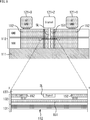
図6において、パッド121-1乃至121-3は、GSGパッドを構成するRF I/Oとして用いられ、パッド121-2にはRF信号が入力される。
図7は、図6中、破線で囲まれるRF I/O近傍の構成を示している。図7上段には、RF I/O近傍の平面図が示されており、図7下段には、図7上段の平面図における線分X-Yでの断面図が示されている。
図7上段に示されるように、RF信号が入力されるパッド121-2とコア回路111とは、信号線SLにより電気的に接続されている。
また、図7下段に示されるように、半導体チップ101は、薄膜配線層131、厚膜配線層132、およびパッシベーション層133からなる断面構造を有している。
薄膜配線層131には、I/Oリング112が形成されている。図7の例では、I/Oリング112は5層の配線層から構成されている。また、薄膜配線層131において、I/Oリング112より上層には、Cuなどの金属からなるグランド面141が設けられている。具体的には、信号線SLの下方の薄膜配線層131においては、I/Oリング112を構成する5層の配線層のうちの最上層の配線層の一部に、グランド面141が形成されている。言い換えると、グランド面141は、I/Oリング112を構成する5層の配線層のうちの4層より上層に形成されている。
また、グランド面141は、コア回路111と電気的に接続される一方、厚膜配線層132に設けられるグランド面142を介して、パッド121-1,121-3と電気的に接続されている。グランド面142は、Cuなどの金属からなり、2層構造を有し、信号線SLに沿ってその両側で延在して形成されている。これにより、パッド121-2とパッド121-1の間、パッド121-2とパッド121-3の間には、それぞれリターンパスが形成される。
このように、図7の例では、信号線SLとグランド面141とは、GSGパッドとコア回路111とに接続されるRF信号伝送線路として、マイクロストリップラインを構成している。
以上の構造によれば、I/Oリング112の配線の一部をカットすることなく、RF I/Oを構成することができるので、図6に示されるように、パッド121-4とパッド121-1との間に高電圧がかかった場合、ESD電流は、低インピーダンスの電流経路Pを経路として放電されるようにすることができ、高周波信号の減衰を抑えつつ、I/Oリングにおいて低インピーダンスの電流経路を確保することが可能となる。
以上のようにして構成されるマイクロストリップラインの特性インピーダンスは、パッド121-2と接続される外部回路のインピーダンスと整合がとれるよう適切に設計される。
このとき、信号線SLとグランド面141との距離dが大きいほど、信号線SLの配線幅wを太くすることができるが、信号線SLとグランド面141との距離dが小さいほど、信号線SLの配線幅wを細くする必要がある。前者の場合、I/Oリング112の配線層を薄くする必要があるので、I/Oリング112の電気抵抗は大きくなるが、RF信号の伝送損失を小さくすることができる。一方、後者の場合、RF信号の伝送損失が大きくなってしまうが、I/Oリング112の配線層を厚くすることができるので、I/Oリング112の電気抵抗を小さくすることができる。
このように、信号線SLとグランド面141との距離dと、信号線SLの配線幅wとはトレードオフの関係にある。
なお、本実施形態の構成においては、グランド面141,142は、I/Oリング112のグランド配線GNDとは分離されている。これにより、他の電源配線とのアイソレーションを確保することができる。
<3.第2の実施形態>
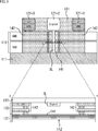
図8は、第2の実施形態の半導体チップにおけるRF I/O近傍の構成を示している。
図8は、第2の実施形態の半導体チップにおけるRF I/O近傍の構成を示している。
図8の例では、薄膜配線層131には、5層の配線層から構成されるI/Oリング112のみが形成され、厚膜配線層132には、グランド面151が設けられている。
また、グランド面151は、コア回路111と電気的に接続される一方、厚膜配線層132においてグランド面151より上層に設けられるグランド面152を介して、パッド121-1,121-3と電気的に接続されている。1層構造のグランド面152は、信号線SLに沿ってその両側で延在して形成されている。
このように、図8の例では、信号線SLとグランド面151とが、GSGパッドとコア回路111とに接続されるRF信号伝送線路として、マイクロストリップラインを構成している。
信号線SLとグランド面151との距離dと、信号線SLの配線幅wとが最適となるよう設計することができれば、本実施形態のように、マイクロストリップラインのグランド面を、単にI/Oリング112より上層の厚膜配線層32に形成することができる。
<4.第3の実施形態>
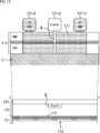
図9は、第3の実施形態の半導体チップにおけるRF I/O近傍の構成を示している。
図9は、第3の実施形態の半導体チップにおけるRF I/O近傍の構成を示している。
図9の例では、薄膜配線層131のグランド面141が、RF信号が入力されるパッド121-2の直下、さらには、パッド121-1,121-3の直下にまで広がって形成されている。
RF I/Oとなるパッドの直下がSi層になっている場合、設計の段階における電磁界解析などのシミュレーションの精度が低下する可能性がある。これに対して、RF I/Oとなるパッドの直下をメタル層にすることで、これらの解析の精度を改善することができる。
<5.第4の実施形態>
図10は、第4の実施形態の半導体チップにおけるRF I/O近傍の構成を示している。
図10は、第4の実施形態の半導体チップにおけるRF I/O近傍の構成を示している。
図10の例では、RF信号が入力されるパッドとして、2つのパッド121-2a,121-2bが設けられている。パッド121-2aとコア回路111とは、信号線SLaにより電気的に接続され、パッド121-2bとコア回路111とは、信号線SLbにより電気的に接続されている。
すなわち、図10において、パッド121-1,121-2a,121-2b,121-3は、GSSG(Ground Signal Signal Ground)パッドを構成するRF I/Oとして用いられる。
このような構成により、コア回路111に、差動RF信号を入力することが可能となる。
<6.第5の実施形態>
図11は、第5の実施形態の半導体チップにおけるRF I/O近傍の構成を示している。
図11は、第5の実施形態の半導体チップにおけるRF I/O近傍の構成を示している。
図11の例では、厚膜配線層132に、パッド121-3と接続されるグランド面142が、信号線SLに沿ってその片側で延在して形成されている。図11において、パッド121-2,121-3は、GS(Ground Signal)パッドを構成するRF I/Oとして用いられ、リターンパスは、パッド121-2とパッド121-3の間のみに形成される。
特性インピーダンスと外部回路のインピーダンスとの整合がとれれば、本実施形態のような構成を採ることも可能である。
<7.第6の実施形態>
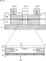
図12は、第6の実施形態の半導体チップにおけるRF I/O近傍の構成を示している。
図12は、第6の実施形態の半導体チップにおけるRF I/O近傍の構成を示している。
図12の例では、信号線SLの下方の薄膜配線層131において、I/Oリング112より上層(5層の配線層のうちの最上層)の一部に、グランド面171が設けられている。厚膜配線層132にはグランド面は設けられておらず、グランド面171は、直接、コア回路111とパッド121-1,121-3とに電気的に接続されている。
図12の例でも、信号線SLとグランド面171とは、RF信号伝送線路として、マイクロストリップラインを構成している。
特性インピーダンスを低くすることができれば、本実施形態のような構成を採ることも可能である。
<8.第7の実施形態>
図13は、第7の実施形態の半導体チップにおけるRF I/O近傍の構成を示している。
図13は、第7の実施形態の半導体チップにおけるRF I/O近傍の構成を示している。
図13の例では、薄膜配線層131に、I/Oリング112のみが形成されている。厚膜配線層132においては、信号線SLと同一面上にグランド面181が設けられている。グランド面181は、2層構造を有し、信号線SLに沿ってその両側で延在して形成されており、それぞれが、コア回路111とパッド121-1,121-3とに電気的に接続されている。
すなわち、図13の例では、信号線SLとグランド面181とが、GSGパッドとコア回路111とに接続されるRF信号伝送線路として、コプレーナ導波路を構成している。
本実施形態の構成においても、I/Oリング112の配線の一部をカットすることなく、RF I/Oを構成することができるので、高周波信号の減衰を抑えつつ、I/Oリングにおいて低インピーダンスの電流経路を確保することが可能となる。
なお、上述した実施形態においては、RF信号が入力されるパッドに対応するESD保護回路122aが、コア回路111内に設けられるものとした。しかしながら、本技術の実施形態においては、マイクロストリップラインやコプレーナ導波路といったRF信号伝送線路が、I/Oリング112より上層に形成されればよい。そこで、図3に示される構成と同様に、ESD保護回路122aがI/Oリング112より下層に形成されるようにしてもよい。
また、上述した実施形態の構成は、単独で適用することもできるし、組み合わせて適用することもできる。
さらに、本技術の実施の形態は、上述した実施の形態に限定されるものではなく、本技術の要旨を逸脱しない範囲において種々の変更が可能である。
また、本技術は以下のような構成をとることができる。
(1)
コア回路を包囲するI/Oリングと、
高周波信号の入出力端子となる第1および第2のパッドと、
前記第1および第2のパッドと前記コア回路とに電気的に接続される高周波信号伝送線路と
を備え、
前記高周波信号伝送線路は、前記I/Oリングより上層に形成される
半導体チップ。
(2)
前記高周波信号伝送線路は、
前記第1のパッドと前記コア回路とに電気的に接続される信号線と、
前記第2のパッドと前記コア回路とに電気的に接続される第1のグランド面と
を有するマイクロストリップラインである
(1)に記載の半導体チップ。
(3)
前記第1のグランド面は、前記I/Oリングより上層で、かつ、前記信号線より下層に形成される
(2)に記載の半導体チップ。
(4)
前記高周波信号伝送線路は、
少なくとも前記第1のグランド面より上層で、前記信号線に沿って前記信号線の両側または片側で延在し、前記第1のグランド面と電気的に接続される第2のグランド面をさらに有する
(2)または(3)に記載の半導体チップ。
(5)
前記第1および第2のパッドは、GSG(Ground Signal Ground)パッドを構成する
(2)乃至(4)のいずれかに記載の半導体チップ。
(6)
前記第1および第2のパッドは、GSSG(Ground Signal Signal Ground)パッドを構成する
(2)乃至(4)のいずれかに記載の半導体チップ。
(7)
前記第1および第2のパッドは、GS(Ground Signal)パッドを構成する
(2)乃至(4)のいずれかに記載の半導体チップ。
(8)
前記第1のグランド面は、前記第1および第2のパッドの直下にまで広がって形成される
(2)乃至(7)のいずれかに記載の半導体チップ。
(9)
前記高周波信号伝送線路は、
前記第1のパッドと前記コア回路とに電気的に接続される信号線と、
前記第2のパッドと前記コア回路とに電気的に接続されるグランド面と
を有するコプレーナ導波路である
(1)に記載の半導体チップ。
(10)
前記信号線および前記グランド線は、前記I/Oリングより上層で、かつ、同一面上に形成される
(9)に記載の半導体チップ。
(11)
前記第1および第2のパッドは、GSG(Ground Signal Ground)パッドを構成する
(9)または(10)に記載の半導体チップ。
(12)
前記コア回路は、前記第1のパッドと前記I/Oリングとに接続されたESD(Electro-Static Discharge)保護回路を有する
(1)乃至(11)のいずれかに記載の半導体チップ。
(1)
コア回路を包囲するI/Oリングと、
高周波信号の入出力端子となる第1および第2のパッドと、
前記第1および第2のパッドと前記コア回路とに電気的に接続される高周波信号伝送線路と
を備え、
前記高周波信号伝送線路は、前記I/Oリングより上層に形成される
半導体チップ。
(2)
前記高周波信号伝送線路は、
前記第1のパッドと前記コア回路とに電気的に接続される信号線と、
前記第2のパッドと前記コア回路とに電気的に接続される第1のグランド面と
を有するマイクロストリップラインである
(1)に記載の半導体チップ。
(3)
前記第1のグランド面は、前記I/Oリングより上層で、かつ、前記信号線より下層に形成される
(2)に記載の半導体チップ。
(4)
前記高周波信号伝送線路は、
少なくとも前記第1のグランド面より上層で、前記信号線に沿って前記信号線の両側または片側で延在し、前記第1のグランド面と電気的に接続される第2のグランド面をさらに有する
(2)または(3)に記載の半導体チップ。
(5)
前記第1および第2のパッドは、GSG(Ground Signal Ground)パッドを構成する
(2)乃至(4)のいずれかに記載の半導体チップ。
(6)
前記第1および第2のパッドは、GSSG(Ground Signal Signal Ground)パッドを構成する
(2)乃至(4)のいずれかに記載の半導体チップ。
(7)
前記第1および第2のパッドは、GS(Ground Signal)パッドを構成する
(2)乃至(4)のいずれかに記載の半導体チップ。
(8)
前記第1のグランド面は、前記第1および第2のパッドの直下にまで広がって形成される
(2)乃至(7)のいずれかに記載の半導体チップ。
(9)
前記高周波信号伝送線路は、
前記第1のパッドと前記コア回路とに電気的に接続される信号線と、
前記第2のパッドと前記コア回路とに電気的に接続されるグランド面と
を有するコプレーナ導波路である
(1)に記載の半導体チップ。
(10)
前記信号線および前記グランド線は、前記I/Oリングより上層で、かつ、同一面上に形成される
(9)に記載の半導体チップ。
(11)
前記第1および第2のパッドは、GSG(Ground Signal Ground)パッドを構成する
(9)または(10)に記載の半導体チップ。
(12)
前記コア回路は、前記第1のパッドと前記I/Oリングとに接続されたESD(Electro-Static Discharge)保護回路を有する
(1)乃至(11)のいずれかに記載の半導体チップ。
101 半導体チップ, 111 コア回路, 112 I/Oリング, GND グランド配線, VDD 電源配線, 121 パッド, 122 ESD保護回路, 131 薄膜配線層, 132 厚膜配線層, 133 パッシベーション層, 141,142 グランド面, SL 信号線
Claims (12)
- コア回路を包囲するI/Oリングと、
高周波信号の入出力端子となる第1および第2のパッドと、
前記第1および第2のパッドと前記コア回路とに電気的に接続される高周波信号伝送線路と
を備え、
前記高周波信号伝送線路は、前記I/Oリングより上層に形成される
半導体チップ。 - 前記高周波信号伝送線路は、
前記第1のパッドと前記コア回路とに電気的に接続される信号線と、
前記第2のパッドと前記コア回路とに電気的に接続される第1のグランド面と
を有するマイクロストリップラインである
請求項1に記載の半導体チップ。 - 前記第1のグランド面は、前記I/Oリングより上層で、かつ、前記信号線より下層に形成される
請求項2に記載の半導体チップ。 - 前記高周波信号伝送線路は、
少なくとも前記第1のグランド面より上層で、前記信号線に沿って前記信号線の両側または片側で延在し、前記第1のグランド面と電気的に接続される第2のグランド面をさらに有する
請求項3に記載の半導体チップ。 - 前記第1および第2のパッドは、GSG(Ground Signal Ground)パッドを構成する
請求項2に記載の半導体チップ。 - 前記第1および第2のパッドは、GSSG(Ground Signal Signal Ground)パッドを構成する
請求項2に記載の半導体チップ。 - 前記第1および第2のパッドは、GS(Ground Signal)パッドを構成する
請求項2に記載の半導体チップ。 - 前記第1のグランド面は、前記第1および第2のパッドの直下にまで広がって形成される
請求項2に記載の半導体チップ。 - 前記高周波信号伝送線路は、
前記第1のパッドと前記コア回路とに電気的に接続される信号線と、
前記第2のパッドと前記コア回路とに電気的に接続されるグランド面と
を有するコプレーナ導波路である
請求項1に記載の半導体チップ。 - 前記信号線および前記グランド線は、前記I/Oリングより上層で、かつ、同一面上に形成される
請求項9に記載の半導体チップ。 - 前記第1および第2のパッドは、GSG(Ground Signal Ground)パッドを構成する
請求項9に記載の半導体チップ。 - 前記コア回路は、前記第1のパッドと前記I/Oリングとに接続されたESD(Electro-Static Discharge)保護回路を有する
請求項1に記載の半導体チップ。
Priority Applications (2)
| Application Number | Priority Date | Filing Date | Title |
|---|---|---|---|
| CN201880008165.XA CN110214370A (zh) | 2017-01-30 | 2018-01-17 | 半导体芯片 |
| US16/477,320 US11373964B2 (en) | 2017-01-30 | 2018-01-17 | Semiconductor chip |
Applications Claiming Priority (2)
| Application Number | Priority Date | Filing Date | Title |
|---|---|---|---|
| JP2017-014301 | 2017-01-30 | ||
| JP2017014301A JP2018125336A (ja) | 2017-01-30 | 2017-01-30 | 半導体チップ |
Publications (1)
| Publication Number | Publication Date |
|---|---|
| WO2018139277A1 true WO2018139277A1 (ja) | 2018-08-02 |
Family
ID=62978348
Family Applications (1)
| Application Number | Title | Priority Date | Filing Date |
|---|---|---|---|
| PCT/JP2018/001086 Ceased WO2018139277A1 (ja) | 2017-01-30 | 2018-01-17 | 半導体チップ |
Country Status (4)
| Country | Link |
|---|---|
| US (1) | US11373964B2 (ja) |
| JP (1) | JP2018125336A (ja) |
| CN (1) | CN110214370A (ja) |
| WO (1) | WO2018139277A1 (ja) |
Citations (7)
| Publication number | Priority date | Publication date | Assignee | Title |
|---|---|---|---|---|
| JPH02226756A (ja) * | 1989-02-28 | 1990-09-10 | Toshiba Corp | 半導体装置 |
| JP2003258152A (ja) * | 2002-02-27 | 2003-09-12 | Apack Communications Inc | 熱バイアを有するモノリシックマイクロ波集積回路パッケージ |
| JP2003347407A (ja) * | 1997-03-14 | 2003-12-05 | Toshiba Corp | マイクロ波集積回路素子 |
| JP2005072607A (ja) * | 2003-08-27 | 2005-03-17 | Samsung Electronics Co Ltd | 静電気保護素子とパワークランプで構成された入出力静電気放電保護セルを具備する集積回路装置 |
| JP2009176535A (ja) * | 2008-01-23 | 2009-08-06 | Mitsubishi Electric Corp | フレキシブル基板用の接続装置及び接続方法 |
| JP2009295855A (ja) * | 2008-06-06 | 2009-12-17 | Renesas Technology Corp | 集積回路 |
| JP2014160750A (ja) * | 2013-02-20 | 2014-09-04 | Nippon Telegr & Teleph Corp <Ntt> | 高周波rf回路 |
Family Cites Families (11)
| Publication number | Priority date | Publication date | Assignee | Title |
|---|---|---|---|---|
| US5185650A (en) * | 1989-02-28 | 1993-02-09 | Kabushiki Kaisha Toshiba | High-speed signal transmission line path structure for semiconductor integrated circuit devices |
| JP3535376B2 (ja) | 1997-03-14 | 2004-06-07 | 株式会社東芝 | マイクロ波集積回路素子 |
| US6878964B1 (en) * | 2003-09-26 | 2005-04-12 | Taiwan Semiconductor Manufacturing Company, Ltd. | Ground-signal-ground pad layout for device tester structure |
| US7178126B2 (en) * | 2004-01-21 | 2007-02-13 | Oki Electric Industry Co., Ltd. | Method of protecting a semiconductor integrated circuit from plasma damage |
| JP2009081293A (ja) * | 2007-09-26 | 2009-04-16 | Oki Semiconductor Co Ltd | 半導体チップ、及び複数の半導体チップが搭載された半導体装置 |
| US20110242712A1 (en) * | 2010-04-01 | 2011-10-06 | Fwu-Juh Huang | Chip with esd protection function |
| US8873209B2 (en) * | 2011-12-19 | 2014-10-28 | Arm Limited | Integrated circuit and method of providing electrostatic discharge protection within such an integrated circuit |
| SG11201403720VA (en) * | 2011-12-30 | 2014-10-30 | Univ Nanyang Tech | Miniature passive structures, high frequency electrostatic discharge protection networks, and high frequency electrostatic discharge protection schemes |
| JP2014096521A (ja) | 2012-11-12 | 2014-05-22 | Renesas Mobile Corp | 半導体装置 |
| KR20140133250A (ko) * | 2013-05-10 | 2014-11-19 | 한국전자통신연구원 | 분포 궤환형 레이저 다이오드 및 그의 제조방법 |
| JP2016062996A (ja) * | 2014-09-16 | 2016-04-25 | 株式会社東芝 | 光検出器 |
-
2017
- 2017-01-30 JP JP2017014301A patent/JP2018125336A/ja active Pending
-
2018
- 2018-01-17 WO PCT/JP2018/001086 patent/WO2018139277A1/ja not_active Ceased
- 2018-01-17 CN CN201880008165.XA patent/CN110214370A/zh active Pending
- 2018-01-17 US US16/477,320 patent/US11373964B2/en active Active
Patent Citations (7)
| Publication number | Priority date | Publication date | Assignee | Title |
|---|---|---|---|---|
| JPH02226756A (ja) * | 1989-02-28 | 1990-09-10 | Toshiba Corp | 半導体装置 |
| JP2003347407A (ja) * | 1997-03-14 | 2003-12-05 | Toshiba Corp | マイクロ波集積回路素子 |
| JP2003258152A (ja) * | 2002-02-27 | 2003-09-12 | Apack Communications Inc | 熱バイアを有するモノリシックマイクロ波集積回路パッケージ |
| JP2005072607A (ja) * | 2003-08-27 | 2005-03-17 | Samsung Electronics Co Ltd | 静電気保護素子とパワークランプで構成された入出力静電気放電保護セルを具備する集積回路装置 |
| JP2009176535A (ja) * | 2008-01-23 | 2009-08-06 | Mitsubishi Electric Corp | フレキシブル基板用の接続装置及び接続方法 |
| JP2009295855A (ja) * | 2008-06-06 | 2009-12-17 | Renesas Technology Corp | 集積回路 |
| JP2014160750A (ja) * | 2013-02-20 | 2014-09-04 | Nippon Telegr & Teleph Corp <Ntt> | 高周波rf回路 |
Also Published As
| Publication number | Publication date |
|---|---|
| CN110214370A (zh) | 2019-09-06 |
| US11373964B2 (en) | 2022-06-28 |
| US20190371748A1 (en) | 2019-12-05 |
| JP2018125336A (ja) | 2018-08-09 |
Similar Documents
| Publication | Publication Date | Title |
|---|---|---|
| CN105051887B (zh) | 半导体装置 | |
| JP6222410B1 (ja) | Esd保護回路、差動伝送線路、コモンモードフィルタ回路、esd保護デバイスおよび複合デバイス | |
| CN205508776U (zh) | 半导体装置 | |
| US9230926B2 (en) | Functionalised redistribution layer | |
| JP5796692B2 (ja) | Esd保護デバイス | |
| JP2008288505A (ja) | コモンモードチョークコイル | |
| US10886730B2 (en) | Filter having an ESD protection device | |
| JP5167671B2 (ja) | 半導体素子 | |
| JP2011014719A (ja) | 半導体装置 | |
| EP2110852B1 (en) | Method and system for mitigating risk of electrostatic discharge for a system on chip (SoC) | |
| JP4770809B2 (ja) | コモンモードチョークコイル及びその製造方法 | |
| WO2018139277A1 (ja) | 半導体チップ | |
| US10804258B2 (en) | ESD protection device and signal transmission line | |
| US7015588B2 (en) | Semiconductor device | |
| CN205282447U (zh) | 半导体装置 | |
| JP6098230B2 (ja) | 半導体装置 | |
| CN112992868B (zh) | 具静电放电防护功能的半导体装置及静电放电的测试方法 | |
| JP7655391B2 (ja) | 過渡電圧吸収素子 | |
| JP2017163054A (ja) | 信号伝送基板 | |
| US20150371961A1 (en) | Semiconductor device |
Legal Events
| Date | Code | Title | Description |
|---|---|---|---|
| 121 | Ep: the epo has been informed by wipo that ep was designated in this application |
Ref document number: 18744730 Country of ref document: EP Kind code of ref document: A1 |
|
| NENP | Non-entry into the national phase |
Ref country code: DE |
|
| 122 | Ep: pct application non-entry in european phase |
Ref document number: 18744730 Country of ref document: EP Kind code of ref document: A1 |