WO2018128046A1 - シリコン単結晶の引き上げ条件演算プログラム、シリコン単結晶のホットゾーンの改良方法、およびシリコン単結晶の育成方法 - Google Patents
シリコン単結晶の引き上げ条件演算プログラム、シリコン単結晶のホットゾーンの改良方法、およびシリコン単結晶の育成方法 Download PDFInfo
- Publication number
- WO2018128046A1 WO2018128046A1 PCT/JP2017/044012 JP2017044012W WO2018128046A1 WO 2018128046 A1 WO2018128046 A1 WO 2018128046A1 JP 2017044012 W JP2017044012 W JP 2017044012W WO 2018128046 A1 WO2018128046 A1 WO 2018128046A1
- Authority
- WO
- WIPO (PCT)
- Prior art keywords
- single crystal
- silicon single
- pulling
- defect
- solid
- Prior art date
- Legal status (The legal status is an assumption and is not a legal conclusion. Google has not performed a legal analysis and makes no representation as to the accuracy of the status listed.)
- Ceased
Links
Images





Classifications
-
- C—CHEMISTRY; METALLURGY
- C30—CRYSTAL GROWTH
- C30B—SINGLE-CRYSTAL GROWTH; UNIDIRECTIONAL SOLIDIFICATION OF EUTECTIC MATERIAL OR UNIDIRECTIONAL DEMIXING OF EUTECTOID MATERIAL; REFINING BY ZONE-MELTING OF MATERIAL; PRODUCTION OF A HOMOGENEOUS POLYCRYSTALLINE MATERIAL WITH DEFINED STRUCTURE; SINGLE CRYSTALS OR HOMOGENEOUS POLYCRYSTALLINE MATERIAL WITH DEFINED STRUCTURE; AFTER-TREATMENT OF SINGLE CRYSTALS OR A HOMOGENEOUS POLYCRYSTALLINE MATERIAL WITH DEFINED STRUCTURE; APPARATUS THEREFOR
- C30B15/00—Single-crystal growth by pulling from a melt, e.g. Czochralski method
- C30B15/20—Controlling or regulating
-
- C—CHEMISTRY; METALLURGY
- C30—CRYSTAL GROWTH
- C30B—SINGLE-CRYSTAL GROWTH; UNIDIRECTIONAL SOLIDIFICATION OF EUTECTIC MATERIAL OR UNIDIRECTIONAL DEMIXING OF EUTECTOID MATERIAL; REFINING BY ZONE-MELTING OF MATERIAL; PRODUCTION OF A HOMOGENEOUS POLYCRYSTALLINE MATERIAL WITH DEFINED STRUCTURE; SINGLE CRYSTALS OR HOMOGENEOUS POLYCRYSTALLINE MATERIAL WITH DEFINED STRUCTURE; AFTER-TREATMENT OF SINGLE CRYSTALS OR A HOMOGENEOUS POLYCRYSTALLINE MATERIAL WITH DEFINED STRUCTURE; APPARATUS THEREFOR
- C30B15/00—Single-crystal growth by pulling from a melt, e.g. Czochralski method
- C30B15/20—Controlling or regulating
- C30B15/22—Stabilisation or shape controlling of the molten zone near the pulled crystal; Controlling the section of the crystal
-
- C—CHEMISTRY; METALLURGY
- C30—CRYSTAL GROWTH
- C30B—SINGLE-CRYSTAL GROWTH; UNIDIRECTIONAL SOLIDIFICATION OF EUTECTIC MATERIAL OR UNIDIRECTIONAL DEMIXING OF EUTECTOID MATERIAL; REFINING BY ZONE-MELTING OF MATERIAL; PRODUCTION OF A HOMOGENEOUS POLYCRYSTALLINE MATERIAL WITH DEFINED STRUCTURE; SINGLE CRYSTALS OR HOMOGENEOUS POLYCRYSTALLINE MATERIAL WITH DEFINED STRUCTURE; AFTER-TREATMENT OF SINGLE CRYSTALS OR A HOMOGENEOUS POLYCRYSTALLINE MATERIAL WITH DEFINED STRUCTURE; APPARATUS THEREFOR
- C30B15/00—Single-crystal growth by pulling from a melt, e.g. Czochralski method
- C30B15/20—Controlling or regulating
- C30B15/206—Controlling or regulating the thermal history of growing the ingot
-
- C—CHEMISTRY; METALLURGY
- C30—CRYSTAL GROWTH
- C30B—SINGLE-CRYSTAL GROWTH; UNIDIRECTIONAL SOLIDIFICATION OF EUTECTIC MATERIAL OR UNIDIRECTIONAL DEMIXING OF EUTECTOID MATERIAL; REFINING BY ZONE-MELTING OF MATERIAL; PRODUCTION OF A HOMOGENEOUS POLYCRYSTALLINE MATERIAL WITH DEFINED STRUCTURE; SINGLE CRYSTALS OR HOMOGENEOUS POLYCRYSTALLINE MATERIAL WITH DEFINED STRUCTURE; AFTER-TREATMENT OF SINGLE CRYSTALS OR A HOMOGENEOUS POLYCRYSTALLINE MATERIAL WITH DEFINED STRUCTURE; APPARATUS THEREFOR
- C30B29/00—Single crystals or homogeneous polycrystalline material with defined structure characterised by the material or by their shape
- C30B29/02—Elements
- C30B29/06—Silicon
Definitions
- the present invention relates to a silicon single crystal pulling condition calculation program, a silicon single crystal hot zone improvement method, and a silicon single crystal growth method.
- Patent Document 1 describes a method of controlling a V / G profile so as to guarantee the effect of a thermomechanical stress field in a single crystal in contact with an interface with respect to the generation of intrinsic point defects.
- V is the pulling rate
- G is the temperature gradient in the growth axis direction.
- Patent Document 1 describes a method for controlling the V / G profile, there is a problem that the hot zone shape and interface shape for doing so are unknown.
- the interface shape described in Patent Document 1 is obtained by numerical analysis and the actual solid-liquid interface shape does not always become such, in this method, the design of the hot zone and its hot There is a problem that the optimum pulling conditions cannot be set in the zone.
- An object of the present invention is to provide a silicon single crystal pulling condition calculation program capable of obtaining a condition in which a defect-free region in each hot zone shape has a maximum value, a method for improving a silicon single crystal hot zone, and a silicon single crystal It is to provide a training method.
- the present invention is characterized in that an optimum pulling condition is obtained by introducing a reference temperature and a solid-liquid interface shape given by the following formula (1) as boundary conditions.
- the silicon single crystal pulling condition calculation program of the present invention is: Silicon for obtaining an optimum value of the solid-liquid interface height h of the solid-liquid interface and the distance Gap between the heat shielding plate constituting the silicon single crystal pulling device and the liquid surface of the silicon melt when growing the silicon single crystal
- a single crystal pulling condition calculation program On the computer, Setting a plurality of pulling conditions based on a plurality of the solid-liquid interface heights h and a distance Gap between the plurality of heat shielding plates and the liquid surface of the silicon melt; For each lifting condition, A step of calculating a heat flux q (W / m 2 ) and a crystal surface temperature T (K) of the pulling device using a comprehensive heat transfer analysis; Based on the calculated heat flux q (W / m 2 ) and the crystal surface temperature T (K), the reference temperature Tref (K
- ⁇ rr, ⁇ and ⁇ zz are stress components perpendicular to the r-plane, ⁇ -plane and z-plane.
- the silicon single crystal hot zone improvement method of the present invention is calculated by computing the silicon single crystal pulling condition calculation program for a plurality of hot zone shapes using the aforementioned silicon single crystal pulling condition calculation program.
- the optimum hot zone is selected from the maximum value of the defect-free area in each hot zone.
- the temperature distribution in the silicon single crystal is calculated using the reference temperature, and the average stress in the silicon single crystal is calculated based on the calculated temperature distribution in the crystal. Is calculated.
- the point defect distribution can be calculated based on the accurate temperature distribution in the crystal and the average stress effect, the maximum value of the defect-free region can be grasped,
- the contour line of the defect-free region can be generated on the two-dimensional map of the distance Gap and the solid-liquid interface height h. Therefore, based on the contour lines on the generated two-dimensional map, the solid-liquid interface height h that gives the maximum defect-free region size and the distance Gap between the heat shielding plate and the liquid surface are selected, and the optimum The pulling conditions can be determined.
- the method for growing a silicon single crystal of the present invention includes: A method for growing a silicon single crystal for growing a silicon single crystal, Using the above-described silicon single crystal pulling condition calculation program, the computer calculates the silicon single crystal pulling condition; The silicon single crystal is pulled up based on the calculated optimum solid-liquid interface height h and the distance Gap between the heat shielding plate and the liquid surface of the silicon single crystal.
- the method for growing a silicon single crystal of the present invention includes: A method for growing a silicon single crystal for growing a silicon single crystal, Using the aforementioned method for improving the hot zone of a silicon single crystal, a step of calculating the pulling condition of the silicon single crystal for a plurality of hot zone shapes; The silicon single crystal is pulled up based on the calculated optimum solid-liquid interface height h and the distance Gap between the heat shielding plate and the liquid surface of the silicon single crystal.
- the optimum solid-liquid interface height h and the distance Gap between the heat shielding plate and the liquid surface are selected by using the silicon single crystal pulling condition calculation program and the hot zone improvement method described above.
- the silicon single crystal can be pulled, the influence of the pulling speed of the silicon single crystal can be reduced and a stable silicon single crystal can be grown.
- the schematic diagram which shows the structure of the pulling apparatus of the silicon single crystal which concerns on embodiment of this invention.
- the flowchart which shows the execution procedure of the raising condition calculation program in the said embodiment.
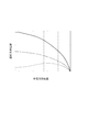
- the graph showing the temperature distribution in the crystal
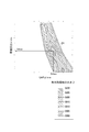
- the schematic diagram which shows distribution of the average stress in the silicon single crystal in the said embodiment.
- the graph which shows the excess amount (relative void
- FIG. 1 is a schematic diagram showing the structure of a silicon single crystal pulling device 1 to which the silicon single crystal growing method according to the embodiment of the present invention can be applied. Yes.
- the pulling device 1 includes a chamber 2 that forms an outer shell, and a crucible 3 that is disposed at the center of the chamber 2.
- the crucible 3 has a double structure composed of an inner quartz crucible 3A and an outer graphite crucible 3B, and is fixed to the upper end of a support shaft 4 that can rotate and move up and down.
- a heater 5 as a resistance heating type heating device surrounding the crucible 3 is provided outside the crucible 3, and a heat insulating material 6 is provided outside the crucible 3 along the inner surface of the chamber 2.
- a lifting shaft 7 such as a wire that rotates coaxially with the support shaft 4 in the reverse direction or in the same direction at a predetermined speed is provided above the crucible 3.
- a seed crystal 8 is attached to the lower end of the pulling shaft 7.
- a water cooling body 11 is disposed as a cylindrical cooling device surrounding the silicon single crystal 10 being grown above the silicon melt 9 in the crucible 3.
- the water-cooled body 11 is made of, for example, a metal having good thermal conductivity such as copper, and is forcibly cooled by cooling water that is circulated inside. This water-cooled body 11 plays a role of accelerating the cooling of the growing silicon single crystal 10 and controlling the temperature gradient in the direction of the pulling axis 7 at the center of the single crystal and the outer periphery of the single crystal.
- the cylindrical heat shielding board 12 is arrange
- the heat shielding plate 12 shields high temperature radiant heat from the silicon melt 9 in the crucible 3, the heater 5, and the side wall of the crucible 3 from the growing silicon single crystal 10, and is a solid liquid that is a crystal growth interface. In the vicinity of the interface, the heat diffusion to the low-temperature water-cooled body 11 is suppressed, and the temperature gradient in the pulling axis direction of the single crystal central portion and the single crystal outer peripheral portion is controlled together with the water-cooled body 11.
- a gas inlet 13 for introducing an inert gas such as Ar gas into the chamber 2 is provided at the upper portion of the chamber 2.
- an exhaust port 14 through which a gas in the chamber 2 is sucked and discharged by driving a vacuum pump (not shown).
- the inert gas introduced into the chamber 2 from the gas inlet 13 descends between the growing silicon single crystal 10 and the water-cooled body 11, and the lower end of the heat shielding plate 12 and the liquid surface of the silicon melt 9 After passing through the gap, the air flows toward the outside of the heat shielding plate 12 and further toward the outside of the crucible 3, and then descends outside the crucible 3 and is discharged from the exhaust port 14.
- a solid material such as polycrystalline silicon filled in the crucible 3 is used as the heater 5 while the chamber 2 is maintained in an inert gas atmosphere under reduced pressure.
- the silicon melt 9 is formed by melting by heating.
- the pulling shaft 7 is lowered to immerse the seed crystal 8 in the silicon melt 9, and the crucible 3 and the pulling shaft 7 are rotated in a predetermined direction while the pulling shaft 7 is gradually pulled up to grow the silicon single crystal 10 connected to the seed crystal 8.
- the computer executes a silicon single crystal pulling condition calculation program based on the flowchart shown in FIG. A distance Gap between the liquid surface of the silicon melt 9 and the heat shielding plate 12 is obtained, and the silicon single crystal 10 is pulled up.
- each step to be calculated by the computer includes a plurality of pulling conditions in which the distance Gap between the liquid surface of the silicon melt 9 and the heat shielding plate 12 and the solid-liquid interface height h are changed.
- Step S1 and for each pulling condition, calculation of heat flux and crystal surface temperature (step S2), calculation of temperature distribution in crystal (step S3), calculation of average stress (step S4)
- step S5 The point defect distribution calculation (step S5) and the defect-free area calculation (step S6) are performed.
- the liquid level and heat of the silicon melt 9 are determined based on the obtained size of the defect-free region in the pulling direction of the silicon single crystal.
- a contour line of a defect-free region is created on the two-dimensional map of the distance Gap to the shielding plate 12 and the solid-liquid interface height h (step S8).
- the optimum distance Gap between the liquid surface of the silicon melt 9 and the heat shielding plate 12 that gives the maximum defect-free region size and the solid-liquid interface height h are selected (step). S9).
- the heat shielding plate 12 is arranged at a distance Gap between the liquid level of the selected silicon melt 9 and the heat shielding plate 12, and the crystal rotation speed, the number of rotations of the crucible 3, the magnetic field strength, etc. are adjusted to obtain a solid liquid.
- a step of setting the interface height h and growing the silicon single crystal 10 is performed (step S10).
- step S10 the step which performs a calculation process is explained in full detail.
- the solid-liquid interface height h is set by appropriately changing in consideration of the crystal rotation speed, the number of rotations of the crucible 3, the magnetic field strength, and the like.
- the range of the diameter (mm) / ( ⁇ 20) of the silicon single crystal 10 to the diameter (mm) / 10 of the silicon single crystal 10 may be used.
- the shape level of the hot zone the shape of the heat shielding plate 12 and the shape / position of the water-cooled body 11 can also be considered.
- step S2 Calculation of heat flux q (W / m 2 ) and crystal surface temperature T (K) by comprehensive heat transfer analysis (step S2)
- the heat flux q (W / m 2 ) and the crystal surface temperature T (K) in the pulling device 1 are calculated using comprehensive heat transfer analysis.
- the heat flux q (W / m 2 ) and the crystal surface temperature T (K) can be calculated by a computer using the thermal flow analysis program CGSim of STR Japan Corporation. Specifically, CGSim calculates the heat flux q (W / m 2 ) and the crystal surface temperature T 1 (K) based on the following formulas (2) to (9).
- step S2 the distribution of the crystal surface temperature of the silicon single crystal 10 and the surrounding heat flux are obtained.
- step S3 Recalculation of temperature distribution in crystal of silicon single crystal 10 (step S3)
- the heat flux q (W / m 2 ) and the crystal surface temperature T (K) of the pulling device 1 are calculated by [3]
- the reference temperature Tref (K) given by the following equation (10) and the solid-liquid interface shape are set as boundary conditions, and the intra-crystal temperature distribution of the silicon single crystal 10 is recalculated using CGSim.
- the temperature distribution T (K) in the crystal is a variable
- ⁇ density
- C heat capacity
- ⁇ thermal conductivity
- the intracrystal temperature of the silicon single crystal 10 is obtained.
- Distribution T is calculated.
- step S3 the temperature distribution in the crystal of the silicon single crystal 10 is obtained as shown in FIG.
- step S4 Calculation of average stress acting in pulling direction in silicon single crystal 10 (step S4)
- the average stress acting in the pulling direction in the silicon single crystal 10 can be calculated using the structure analysis software ABAQUS.
- various methods such as a finite element method, a finite volume method, a finite difference method, can be used.
- the physical property values used for the calculation the following formula (15) to formula (20) can be used.
- step S4 the distribution of the average stress along the pulling direction of the silicon single crystal 10 is obtained as shown in FIG.
- the numerical value in FIG. 4 shows an average stress value (au), where positive is tensile stress and negative is compressive stress.
- step S4 Calculation of point defect distribution in pulling direction of silicon single crystal 10 (step S4) The calculation of the defect distribution inside the silicon single crystal 10 is carried out using the temperature distribution T in the silicon single crystal 10 calculated in [4] and the average stress in the pulling direction of the silicon single crystal 10 calculated in [5]. Based on formula (21), formula (25) is obtained as a basic formula.
- Formula (21) represents the diffusion flux under the temperature gradient of the silicon single crystal 10.
- the first term of the equation (22) shows the concentration change (diffusion term) of point defects due to diffusion, and the second term shows the effect of concentration transfer (advection term) caused by the movement of the silicon single crystal 10 by pulling.
- the third term of the formula (22) is a pair annihilation reaction term between vacancies and interstitial silicon. Equation (23) shows the reaction constant of the pair annihilation reaction, ⁇ G IV is the barrier energy for pair annihilation, and ac is the critical distance at which pair annihilation occurs.
- the point defect concentration during growth can be obtained by solving the equation (22) under the boundary condition that the point defect concentration on the free surface of the silicon single crystal 10 is the thermal equilibrium concentration at the temperature at that position. Note that the point defect concentration distribution predicted by the calculation model and the quality of correspondence by experiment depend on the following 12 parameter settings.
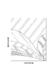
- FIG. 6A is an X-ray transmission photograph after heat treatment at 780 ° C. ⁇ 3 hr and 1000 ° C. ⁇ 16 hr, showing the distribution of point defects in the crystal
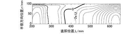
- FIGS. 6B and 6C show the contour lines of relative vacancy supersaturation.
- the actual point defect distribution is in the state shown in FIG. 6A
- the reference temperature Tref and the stress effect are not taken into consideration
- the calculated point defect distribution becomes the actual point defect as shown in FIG. 6B. This is very different from the defect distribution.
- FIG. 6C since the reference temperature Tref and the stress effect are taken into account, as shown in FIG. 6C, a point defect distribution very close to the actual point defect distribution can be obtained.
- step S6 The calculation of the defect-free region of the silicon single crystal 10 is performed by calculating a point defect concentration distribution region that is equal to or less than a predetermined threshold based on the point defect concentration distribution in the pulling direction of the silicon single crystal 10 obtained in [6]. Find as an area. Specifically, in the present embodiment, a region where the interstitial defect region is ⁇ 0.2129 ⁇ 10 13 / cm 3 or less and the vacancy defect region is 0.5787 ⁇ 10 13 / cm 3 or less is defined as a defect-free region. Looking for. When the defect-free region is obtained by calculating the defect-free region of the silicon single crystal 10, the distribution of the defect-free region corresponding to the radial position of the silicon single crystal 10 can be obtained as shown in a region Z1 shown in FIG. it can.
- the distance Gap between the liquid surface of the silicon melt 9 and the heat shielding plate 12 and the solid-liquid interface height h A contour line of a defect-free region is generated on the two-dimensional map (step S8).
- the distance Gap and the solid-liquid interface height h between the liquid surface of the silicon melt 9 and the heat shielding plate 12 in the largest defect-free region are selected (step S9).
- the optimum distance Gmax between the liquid surface of the silicon melt 9 and the heat shielding plate 12 and the optimum solid-liquid interface height hmax are selected as one point in the largest defect-free region Z1.
- the distance Gap between the liquid surface of the silicon melt 9 and the heat shielding plate 12 is set to an optimum distance Gmax, the crystal rotation speed of the silicon single crystal 10, the rotation speed of the crucible 3, and the magnetic field strength. Etc. are changed and the solid-liquid interface height h is set to hmax, and then the silicon single crystal 10 is grown (step S10).
- the defect-free region on the two-dimensional map of the distance Gap between the liquid surface of the silicon melt 9 and the heat shielding plate 12 and the solid-liquid interface height h in each hot zone By comparing the maximum values of the contour lines, it can be confirmed whether the change of the hot zone can expand the defect-free region.
- SYMBOLS 1 Lifting device, 2 ... Chamber, 3 ... Crucible crucible, 3A ... Quartz crucible, 3B ... Graphite crucible, 4 ... Support shaft, 5 ... Heater, 6 ... Heat insulating material, 7 ... Lifting shaft, 8 ... Seed crystal, 9 ... Raw material Melt, 10 ... silicon single crystal, 11 ... water-cooled body, 12 ... heat shielding plate, 13 ... gas inlet, 14 ... exhaust port.
Landscapes
- Chemical & Material Sciences (AREA)
- Engineering & Computer Science (AREA)
- Crystallography & Structural Chemistry (AREA)
- Materials Engineering (AREA)
- Metallurgy (AREA)
- Organic Chemistry (AREA)
- Crystals, And After-Treatments Of Crystals (AREA)
Abstract
引き上げ条件演算プログラムは、固液界面高さおよびシリコン単結晶の液面と熱遮蔽板との距離に応じた複数の引き上げ条件を設定し、各引き上げ条件について、熱流束(q)(W/m2)および結晶表面温度(T)を演算するステップ(S2)、下記式(1)で与えられる参照温度(Tref)と、固液界面形状とを境界条件として設定するステップと、結晶内温度分布を再演算するステップ(S3)、シリコン単結晶内の平均応力を演算するステップ(S4)、平均応力、結晶内温度分布に基づいて、引き上げ方向の欠陥分布を演算するステップ(S5)、引き上げ方向の無欠陥領域を求めるステップ(S6)、距離および固液界面高さの二次元マップ上に、無欠陥領域の大きさの等高線を生成するステップ(S8)をコンピュータに実行させる。
Description
本発明は、シリコン単結晶の引き上げ条件演算プログラム、シリコン単結晶のホットゾーンの改良方法、およびシリコン単結晶の育成方法に関する。
従来、シリコン単結晶の育成方法として、シリコン単結晶内部に作用する応力効果を考慮して、無欠陥のシリコン単結晶の育成方法が提案されている(たとえば、特許文献1参照)。
特許文献1では、界面に接する単結晶中の熱機械応力場の効果を内因性点欠陥の発生に関して保証するようにV/Gプロフィールを制御する方法が記載されている。ここで、Vは引上げ速度、Gは成長軸方向の温度勾配である。
特許文献1では、界面に接する単結晶中の熱機械応力場の効果を内因性点欠陥の発生に関して保証するようにV/Gプロフィールを制御する方法が記載されている。ここで、Vは引上げ速度、Gは成長軸方向の温度勾配である。
しかしながら、前記特許文献1に記載の技術は、V/Gプロフィールを制御する方法が記載されているが、その様にするためのホットゾーン形状、界面形状はわからないという課題がある。
また、前記特許文献1に記載されている界面形状は数値解析により求められるものであって、実際の固液界面形状がその様になるとは限らないため、本手法ではホットゾーンの設計ならびにそのホットゾーンでの最適な引上げ条件を設定できない課題がある。
また、前記特許文献1に記載されている界面形状は数値解析により求められるものであって、実際の固液界面形状がその様になるとは限らないため、本手法ではホットゾーンの設計ならびにそのホットゾーンでの最適な引上げ条件を設定できない課題がある。
本発明の目的は、各ホットゾーン形状での無欠陥領域が最大値となる条件を求めることができるシリコン単結晶の引き上げ条件演算プログラム、シリコン単結晶のホットゾーンの改良方法、およびシリコン単結晶の育成方法を提供することにある。
本発明は、下記式(1)で与えられる参照温度と固液界面形状を境界条件として導入することにより、最適な引き上げ条件を求めることとしたことに特徴がある。
すなわち、本発明のシリコン単結晶の引き上げ条件演算プログラムは、
シリコン単結晶を育成するに際し、固液界面の固液界面高さhと、前記シリコン単結晶の引き上げ装置を構成する熱遮蔽板とシリコン融液の液面との距離Gapの最適値を求めるシリコン単結晶の引き上げ条件演算プログラムであって、
コンピュータに、
複数の前記固液界面高さh、および複数の前記熱遮蔽板とシリコン融液の液面との距離Gapに基づいて、複数の引き上げ条件を設定するステップと、
それぞれの引き上げ条件について、
総合伝熱解析を用いて、前記引き上げ装置の熱流束q(W/m2)および結晶表面温度T(K)を演算するステップと、
演算された前記熱流束q(W/m2)および前記結晶表面温度T(K)に基づいて、下記式(1)で与えられる参照温度Tref(K)と、固液界面形状とを境界条件として設定するステップと、
設定された境界条件に基づいて、前記シリコン単結晶の結晶内温度分布を再演算するステップと、
再演算された前記シリコン単結晶の結晶内温度分布に基づいて、構造解析を用いて、前記シリコン単結晶内に生じる平均応力σmeanを演算するステップと、
演算された前記シリコン単結晶内の平均応力σmean、および、再演算された前記シリコン単結晶の結晶内温度分布に基づいて、前記シリコン単結晶の引き上げ方向の欠陥分布を演算するステップと、
演算された前記シリコン単結晶の引き上げ方向の欠陥分布に基づいて、前記シリコン単結晶の引き上げ方向の無欠陥領域を求めるステップと、
を実行させ、
求められたそれぞれの引き上げ条件における前記シリコン単結晶の引き上げ方向の無欠陥領域の大きさに基づいて、前記熱遮蔽板とシリコン融液の液面との距離Gapおよび前記固液界面高さhの二次元マップ上に、前記無欠陥領域の等高線を生成するステップと、
生成された二次元マップ上の等高線に基づいて、最大の前記無欠陥領域の大きさを与える固液界面高さh、および前記熱遮蔽板とシリコン融液の液面との距離Gapを選択するステップと、
を実行させることを特徴とする。
ここで、平均応力σmeanは、
σmean=(σrr+σθθ+σzz)/3により求められる。そして、σrr、σθθならびにσzzは、r面、θ面そしてz面に垂直な応力成分である。
すなわち、本発明のシリコン単結晶の引き上げ条件演算プログラムは、
シリコン単結晶を育成するに際し、固液界面の固液界面高さhと、前記シリコン単結晶の引き上げ装置を構成する熱遮蔽板とシリコン融液の液面との距離Gapの最適値を求めるシリコン単結晶の引き上げ条件演算プログラムであって、
コンピュータに、
複数の前記固液界面高さh、および複数の前記熱遮蔽板とシリコン融液の液面との距離Gapに基づいて、複数の引き上げ条件を設定するステップと、
それぞれの引き上げ条件について、
総合伝熱解析を用いて、前記引き上げ装置の熱流束q(W/m2)および結晶表面温度T(K)を演算するステップと、
演算された前記熱流束q(W/m2)および前記結晶表面温度T(K)に基づいて、下記式(1)で与えられる参照温度Tref(K)と、固液界面形状とを境界条件として設定するステップと、
設定された境界条件に基づいて、前記シリコン単結晶の結晶内温度分布を再演算するステップと、
再演算された前記シリコン単結晶の結晶内温度分布に基づいて、構造解析を用いて、前記シリコン単結晶内に生じる平均応力σmeanを演算するステップと、
演算された前記シリコン単結晶内の平均応力σmean、および、再演算された前記シリコン単結晶の結晶内温度分布に基づいて、前記シリコン単結晶の引き上げ方向の欠陥分布を演算するステップと、
演算された前記シリコン単結晶の引き上げ方向の欠陥分布に基づいて、前記シリコン単結晶の引き上げ方向の無欠陥領域を求めるステップと、
を実行させ、
求められたそれぞれの引き上げ条件における前記シリコン単結晶の引き上げ方向の無欠陥領域の大きさに基づいて、前記熱遮蔽板とシリコン融液の液面との距離Gapおよび前記固液界面高さhの二次元マップ上に、前記無欠陥領域の等高線を生成するステップと、
生成された二次元マップ上の等高線に基づいて、最大の前記無欠陥領域の大きさを与える固液界面高さh、および前記熱遮蔽板とシリコン融液の液面との距離Gapを選択するステップと、
を実行させることを特徴とする。
ここで、平均応力σmeanは、
σmean=(σrr+σθθ+σzz)/3により求められる。そして、σrr、σθθならびにσzzは、r面、θ面そしてz面に垂直な応力成分である。

但し、
ε=0.55:シリコン単結晶の熱輻射率
σ=5.67×10⁻⁸(W/m2/K4):ステファン-ボルツマン係数
ε=0.55:シリコン単結晶の熱輻射率
σ=5.67×10⁻⁸(W/m2/K4):ステファン-ボルツマン係数
本発明のシリコン単結晶のホットゾーンの改良方法は、複数のホットゾーン形状について、前述したシリコン単結晶の引き上げ条件演算プログラムを用いて、コンピュータに前記シリコン単結晶の引き上げ条件を演算し、演算されたそれぞれのホットゾーンにおける無欠陥領域の最大値から、最適なホットゾーンを選択することを特徴とする。
本発明によれば、設定されたそれぞれの引き上げ条件について、参照温度を用いてシリコン単結晶の結晶内温度分布を演算し、演算された結晶内温度分布に基づいて、シリコン単結晶内の平均応力を演算している。そして、精度の高い結晶内温度分布と平均応力効果に基づいて、点欠陥分布を演算することができるため、無欠陥領域の最大値を把握することができ、これを熱遮蔽板と液面との距離Gap、および固液界面高さhの二次元マップ上に、無欠陥領域の等高線を生成することができる。したがって、生成された二次元マップ上の等高線に基づいて、最大の無欠陥領域の大きさを与える固液界面高さh、および熱遮蔽板と液面との距離Gapを選択して、最適な引き上げ条件を求めることができる。
本発明のシリコン単結晶の育成方法は、
シリコン単結晶を育成するシリコン単結晶の育成方法であって、
前述したシリコン単結晶の引き上げ条件演算プログラムを用いて、コンピュータに前記シリコン単結晶の引き上げ条件を演算する工程と、
演算された最適な固液界面高さhおよび前記熱遮蔽板とシリコン単結晶の液面との距離Gapに基づいて、前記シリコン単結晶の引き上げを行うことを特徴とする。
シリコン単結晶を育成するシリコン単結晶の育成方法であって、
前述したシリコン単結晶の引き上げ条件演算プログラムを用いて、コンピュータに前記シリコン単結晶の引き上げ条件を演算する工程と、
演算された最適な固液界面高さhおよび前記熱遮蔽板とシリコン単結晶の液面との距離Gapに基づいて、前記シリコン単結晶の引き上げを行うことを特徴とする。
本発明のシリコン単結晶の育成方法は、
シリコン単結晶を育成するシリコン単結晶の育成方法であって、
前述したシリコン単結晶のホットゾーンの改良方法を用いて、複数のホットゾーン形状について、前記シリコン単結晶の引き上げ条件を演算する工程と、
演算された最適な固液界面高さhおよび前記熱遮蔽板とシリコン単結晶の液面との距離Gapに基づいて、前記シリコン単結晶の引き上げを行うことを特徴とする。
シリコン単結晶を育成するシリコン単結晶の育成方法であって、
前述したシリコン単結晶のホットゾーンの改良方法を用いて、複数のホットゾーン形状について、前記シリコン単結晶の引き上げ条件を演算する工程と、
演算された最適な固液界面高さhおよび前記熱遮蔽板とシリコン単結晶の液面との距離Gapに基づいて、前記シリコン単結晶の引き上げを行うことを特徴とする。
この発明によれば、前述したシリコン単結晶の引き上げ条件演算プログラムおよびホットゾーンの改良方法を用いることにより、最適な固液界面高さhおよび熱遮蔽板と液面との距離Gapを選択した上で、シリコン単結晶の引き上げを行うことができるため、シリコン単結晶の引き上げ速度の影響を少なくして、安定したシリコン単結晶を育成することができる。
[1]シリコン単結晶の引き上げ装置1の構造
図1には、本発明の実施形態に係るシリコン単結晶の育成方法を適用できるシリコン単結晶の引き上げ装置1の構造を表す模式図が示されている。引き上げ装置1は、外郭を構成するチャンバ2と、チャンバ2の中心部に配置されるルツボ3とを備える。
ルツボ3は、内側の石英ルツボ3Aと、外側の黒鉛ルツボ3Bとから構成される二重構造であり、回転および昇降が可能な支持軸4の上端部に固定されている。
図1には、本発明の実施形態に係るシリコン単結晶の育成方法を適用できるシリコン単結晶の引き上げ装置1の構造を表す模式図が示されている。引き上げ装置1は、外郭を構成するチャンバ2と、チャンバ2の中心部に配置されるルツボ3とを備える。
ルツボ3は、内側の石英ルツボ3Aと、外側の黒鉛ルツボ3Bとから構成される二重構造であり、回転および昇降が可能な支持軸4の上端部に固定されている。
ルツボ3の外側には、ルツボ3を囲む抵抗加熱式の加熱装置としてのヒータ5が設けられ、その外側には、チャンバ2の内面に沿って断熱材6が設けられている。
ルツボ3の上方には、支持軸4と同軸上で逆方向または同一方向に所定の速度で回転するワイヤなどの引き上げ軸7が設けられている。この引き上げ軸7の下端には種結晶8が取り付けられている。
ルツボ3の上方には、支持軸4と同軸上で逆方向または同一方向に所定の速度で回転するワイヤなどの引き上げ軸7が設けられている。この引き上げ軸7の下端には種結晶8が取り付けられている。
チャンバ2内には、ルツボ3内のシリコン融液9の上方で育成中のシリコン単結晶10を囲む円筒状の冷却装置としての水冷体11が配置されている。
水冷体11は、例えば、銅などの熱伝導性の良好な金属からなり、内部に流通される冷却水により強制的に冷却される。この水冷体11は、育成中のシリコン単結晶10の冷却を促進し、単結晶中心部および単結晶外周部の引き上げ軸7方向の温度勾配を制御する役割を担う。
水冷体11は、例えば、銅などの熱伝導性の良好な金属からなり、内部に流通される冷却水により強制的に冷却される。この水冷体11は、育成中のシリコン単結晶10の冷却を促進し、単結晶中心部および単結晶外周部の引き上げ軸7方向の温度勾配を制御する役割を担う。
さらに、水冷体11の外周面および下端面を包囲するように、筒状の熱遮蔽板12が配置されている。
熱遮蔽板12は、育成中のシリコン単結晶10に対して、ルツボ3内のシリコン融液9やヒータ5やルツボ3の側壁からの高温の輻射熱を遮断するとともに、結晶成長界面である固液界面の近傍に対しては、低温の水冷体11への熱の拡散を抑制し、単結晶中心部および単結晶外周部の引き上げ軸方向の温度勾配を水冷体11とともに制御する役割を担う。
熱遮蔽板12は、育成中のシリコン単結晶10に対して、ルツボ3内のシリコン融液9やヒータ5やルツボ3の側壁からの高温の輻射熱を遮断するとともに、結晶成長界面である固液界面の近傍に対しては、低温の水冷体11への熱の拡散を抑制し、単結晶中心部および単結晶外周部の引き上げ軸方向の温度勾配を水冷体11とともに制御する役割を担う。
チャンバ2の上部には、Arガスなどの不活性ガスをチャンバ2内に導入するガス導入口13が設けられている。チャンバ2の下部には、図示しない真空ポンプの駆動によりチャンバ2内の気体を吸引して排出する排気口14が設けられている。
ガス導入口13からチャンバ2内に導入された不活性ガスは、育成中のシリコン単結晶10と水冷体11との間を下降し、熱遮蔽板12の下端とシリコン融液9の液面との隙間を経た後、熱遮蔽板12の外側、さらにルツボ3の外側に向けて流れ、その後にルツボ3の外側を下降し、排気口14から排出される。
ガス導入口13からチャンバ2内に導入された不活性ガスは、育成中のシリコン単結晶10と水冷体11との間を下降し、熱遮蔽板12の下端とシリコン融液9の液面との隙間を経た後、熱遮蔽板12の外側、さらにルツボ3の外側に向けて流れ、その後にルツボ3の外側を下降し、排気口14から排出される。
このような引き上げ装置1を用いたシリコン単結晶10の育成の際、チャンバ2内を減圧下の不活性ガス雰囲気に維持した状態で、ルツボ3に充填した多結晶シリコンなどの固形原料をヒータ5の加熱により溶融させ、シリコン融液9を形成する。ルツボ3内にシリコン融液9が形成されると、引き上げ軸7を下降させて種結晶8をシリコン融液9に浸漬し、ルツボ3および引き上げ軸7を所定の方向に回転させながら、引き上げ軸7を徐々に引き上げ、これにより種結晶8に連なったシリコン単結晶10を育成する。
このような引き上げ装置1によりシリコン単結晶を育成する際、シリコン融液9のメニスカス線と、シリコン単結晶の固液界面との間の固液界面高さhと、シリコン融液9の液面と熱遮蔽板12との距離Gapとの最適値を求めるには、図2に示されるフローチャートに基づくシリコン単結晶の引き上げ条件演算プログラムをコンピュータに実行させ、最適な固液界面高さhと、シリコン融液9の液面と熱遮蔽板12との距離Gapを求め、シリコン単結晶10の引き上げを行う。
具体的には、コンピュータに演算させる各ステップは、図2に示すように、シリコン融液9の液面と熱遮蔽板12との距離Gapおよび固液界面高さhを変更した複数の引き上げ条件の設定(ステップS1)を行い、ぞれぞれの引き上げ条件について、熱流束および結晶表面温度の演算(ステップS2)、結晶内温度分布の演算(ステップS3)、平均応力の演算(ステップS4)、点欠陥分布の演算(ステップS5)、および無欠陥領域の演算(ステップS6)を行う。
そして、すべての引き上げ条件について無欠陥領域の演算が終了したら(ステップS7)、求められた前記シリコン単結晶の引き上げ方向の無欠陥領域の大きさに基づいて、シリコン融液9の液面と熱遮蔽板12との距離Gap、および前記固液界面高さhの二次元マップ上に無欠陥領域の等高線を作成する(ステップS8)。
そして、すべての引き上げ条件について無欠陥領域の演算が終了したら(ステップS7)、求められた前記シリコン単結晶の引き上げ方向の無欠陥領域の大きさに基づいて、シリコン融液9の液面と熱遮蔽板12との距離Gap、および前記固液界面高さhの二次元マップ上に無欠陥領域の等高線を作成する(ステップS8)。
作成されたマップに基づいて、最大の無欠陥領域の大きさを与える、シリコン融液9の液面と熱遮蔽板12との最適な距離Gap、および固液界面高さhを選択する(ステップS9)。
最後に、選択されたシリコン融液9の液面と熱遮蔽板12との距離Gapに熱遮蔽板12を配置し、結晶回転速度、ルツボ3の回転数、磁場強度等を調整して固液界面高さhを設定し、シリコン単結晶10を育成する工程を実施する(ステップS10)。
以下、演算処理を行うステップについて詳述する。
最後に、選択されたシリコン融液9の液面と熱遮蔽板12との距離Gapに熱遮蔽板12を配置し、結晶回転速度、ルツボ3の回転数、磁場強度等を調整して固液界面高さhを設定し、シリコン単結晶10を育成する工程を実施する(ステップS10)。
以下、演算処理を行うステップについて詳述する。
[2]引き上げ条件の設定(ステップS1)
まず、シリコン融液9の液面と熱遮蔽板12との距離Gapと、固液界面高さhを複数設定し、複数の引き上げ条件の設定を行う。具体的には、シリコン融液9の液面と熱遮蔽板12との距離Gapについて7水準、固液界面高さhについて7水準を設定し、7×7=49水準の引き上げ条件の設定を行う。なお、シリコン融液9の液面と熱遮蔽板12との距離Gapおよび固液界面高さhの水準は、任意に設定することができる。固液界面高さhの設定は、結晶回転速度、ルツボ3の回転数、磁場強度等を考慮して適宜変更して設定する。固液界面高さhの設定が不明の場合は、シリコン単結晶10の直径(mm)÷(-20)からシリコン単結晶10の直径(mm)÷10の範囲としてもよい。
また、ホットゾーンの形状水準としては、熱遮蔽板12の形状、水冷体11の形状・位置も考慮することができる。
まず、シリコン融液9の液面と熱遮蔽板12との距離Gapと、固液界面高さhを複数設定し、複数の引き上げ条件の設定を行う。具体的には、シリコン融液9の液面と熱遮蔽板12との距離Gapについて7水準、固液界面高さhについて7水準を設定し、7×7=49水準の引き上げ条件の設定を行う。なお、シリコン融液9の液面と熱遮蔽板12との距離Gapおよび固液界面高さhの水準は、任意に設定することができる。固液界面高さhの設定は、結晶回転速度、ルツボ3の回転数、磁場強度等を考慮して適宜変更して設定する。固液界面高さhの設定が不明の場合は、シリコン単結晶10の直径(mm)÷(-20)からシリコン単結晶10の直径(mm)÷10の範囲としてもよい。
また、ホットゾーンの形状水準としては、熱遮蔽板12の形状、水冷体11の形状・位置も考慮することができる。
[3]総合伝熱解析による熱流束q(W/m2)および結晶表面温度T(K)の演算(ステップS2)
引き上げ装置1内の熱流束q(W/m2)および結晶表面温度T(K)は、総合伝熱解析を用いて演算する。熱流束q(W/m2)および結晶表面温度T(K)の演算は、STRジャパン株式会社の熱流動解析プログラムCGSimを用いてコンピュータに演算させることができる。
具体的には、CGSimでは、以下の式(2)~式(9)に基づいて、熱流束q(W/m2)および結晶表面温度T1(K)の演算を行う。
引き上げ装置1内の熱流束q(W/m2)および結晶表面温度T(K)は、総合伝熱解析を用いて演算する。熱流束q(W/m2)および結晶表面温度T(K)の演算は、STRジャパン株式会社の熱流動解析プログラムCGSimを用いてコンピュータに演算させることができる。
具体的には、CGSimでは、以下の式(2)~式(9)に基づいて、熱流束q(W/m2)および結晶表面温度T1(K)の演算を行う。






ここで、
ρ:密度
ρ0:参照密度
ベクトルu:引き上げ速度
τ:応力テンソル
ベクトルg:重力ベクトル
μeff=μmolecuilar+μt:有効動的粘性率(分子粘性と乱流粘性の和)
cp:比熱
T:温度
φi:ith passive species
λeff:有効熱伝導率
である。
ρ:密度
ρ0:参照密度
ベクトルu:引き上げ速度
τ:応力テンソル
ベクトルg:重力ベクトル
μeff=μmolecuilar+μt:有効動的粘性率(分子粘性と乱流粘性の和)
cp:比熱
T:温度
φi:ith passive species
λeff:有効熱伝導率
である。
具体的な熱流束q(W/m2)および結晶表面温度T(K)の演算例としては、
Global modelling of heat transfer in crystal growth furnaces
F.DUPRET,P.NICODEME,Y.RYCKMANS,P.WOUTERS,M.J.CROCHET
Int.J.Heat Mass Transfer. Vol.33 No.9,pp,1849-1871,1990
に詳細に説明してある。
ステップS2の実行により、シリコン単結晶10の結晶表面温度の分布、および周囲の熱流束が求められる。
Global modelling of heat transfer in crystal growth furnaces
F.DUPRET,P.NICODEME,Y.RYCKMANS,P.WOUTERS,M.J.CROCHET
Int.J.Heat Mass Transfer. Vol.33 No.9,pp,1849-1871,1990
に詳細に説明してある。
ステップS2の実行により、シリコン単結晶10の結晶表面温度の分布、および周囲の熱流束が求められる。
[4]シリコン単結晶10の結晶内温度分布の再計算(ステップS3)
[3]により引き上げ装置1の熱流束q(W/m2)および結晶表面温度T(K)が演算されたら、下記式(10)で与えられる参照温度Tref(K)と、固液界面形状とを境界条件として設定し、シリコン単結晶10の結晶内温度分布を、CGSimを用いて再演算する。
[3]により引き上げ装置1の熱流束q(W/m2)および結晶表面温度T(K)が演算されたら、下記式(10)で与えられる参照温度Tref(K)と、固液界面形状とを境界条件として設定し、シリコン単結晶10の結晶内温度分布を、CGSimを用いて再演算する。

但し、
ε=0.55:シリコン単結晶の熱輻射率
σ=5.67×10⁻⁸(W/m2/K4):ステファン-ボルツマン係数
シリコン単結晶10の結晶内部温度分布の再演算は、シリコン単結晶10の温度分布が引き上げ軸7に対称であり、定常状態であり、シリコン単結晶10内の熱の発生、消失がないものと仮定し、円柱座標系(r,θ,z)の式(11)で与えられる伝熱方程式を解くことにより演算することができる。
ε=0.55:シリコン単結晶の熱輻射率
σ=5.67×10⁻⁸(W/m2/K4):ステファン-ボルツマン係数
シリコン単結晶10の結晶内部温度分布の再演算は、シリコン単結晶10の温度分布が引き上げ軸7に対称であり、定常状態であり、シリコン単結晶10内の熱の発生、消失がないものと仮定し、円柱座標系(r,θ,z)の式(11)で与えられる伝熱方程式を解くことにより演算することができる。

但し、結晶内温度分布T(K)は変数であり、ρ(密度)、C(熱容量)、λ(熱伝導率)は物性値である。また、速度ベクトルV=(u,v,w)であり、u、vは、下記式(12)、式(13)で与えられる。

なお、シリコン単結晶10の引き上げ速度vのみを考える場合、u=0、w=v0であり、式(12)および式(13)は、容易に解くことができ、下記式(14)を用いて事前に与えればよい。

式(10)で与えられる参照温度Trefと、与えた固液界面形状に応じた境界条件に基づいて、式(11)で与えられる伝熱方程式を解くことにより、シリコン単結晶10の結晶内温度分布Tが演算される。
ステップS3の実行により、図3に示すように、シリコン単結晶10の結晶内温度分布が求められる。
ステップS3の実行により、図3に示すように、シリコン単結晶10の結晶内温度分布が求められる。
[5]シリコン単結晶10内の引き上げ方向に作用する平均応力の演算(ステップS4)
シリコン単結晶10内の引き上げ方向に作用する平均応力は、構造解析ソフトABAQUSを用いて演算することができる。なお、構造解析方法としては、有限要素法、有限体積法、有限差分法等種々の方法を用いることができる。
演算に用いる物性値としては、下記(15)から式(20)を用いることができる。
シリコン単結晶10内の引き上げ方向に作用する平均応力は、構造解析ソフトABAQUSを用いて演算することができる。なお、構造解析方法としては、有限要素法、有限体積法、有限差分法等種々の方法を用いることができる。
演算に用いる物性値としては、下記(15)から式(20)を用いることができる。


ステップS4の実行により、図4に示すように、シリコン単結晶10の引き上げ方向に沿った平均応力の分布が求められる。図4中の数値は平均応力値(au)を示し、正が引っ張り応力、負が圧縮応力である。
[6]シリコン単結晶10の引き上げ方向の点欠陥分布の演算(ステップS4)
シリコン単結晶10内部の欠陥分布の演算は、[4]で演算されたシリコン単結晶10の結晶内温度分布Tと、[5]で演算されたシリコン単結晶10の引き上げ方向の平均応力とに基づいて、式(21)から式(25)を基礎式として求められる。
シリコン単結晶10内部の欠陥分布の演算は、[4]で演算されたシリコン単結晶10の結晶内温度分布Tと、[5]で演算されたシリコン単結晶10の引き上げ方向の平均応力とに基づいて、式(21)から式(25)を基礎式として求められる。


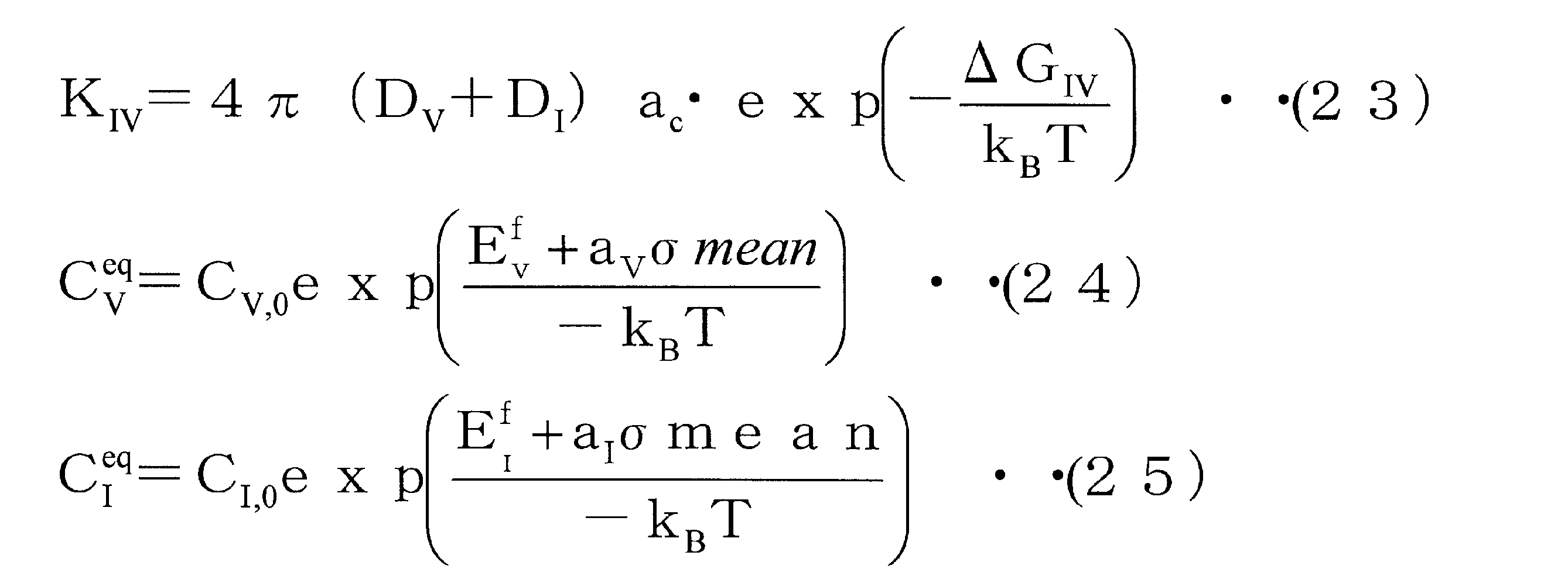
式(21)は、シリコン単結晶10の温度勾配下における拡散フラックスを表す。式(22)の第1項は、拡散による点欠陥の濃度変化(拡散項)を示し、第2項は、シリコン単結晶10が引き上げによって移動することによる濃度移動の効果(移流項)を示す。式(22)の第3項は、空孔と格子間シリコンの間の対消滅反応項である。
式(23)は、対消滅反応の反応定数を示し、ΔGIVは、対消滅の障壁エネルギー、acは対消滅が生じる臨界距離である。
式(23)は、対消滅反応の反応定数を示し、ΔGIVは、対消滅の障壁エネルギー、acは対消滅が生じる臨界距離である。
シリコン単結晶10の自由表面における点欠陥濃度は、その位置の温度における熱平衡濃度であるという境界条件のもとで式(22)を解くことにより、成長中の点欠陥濃度を求めることができる。
なお、計算モデルにより予測される点欠陥濃度分布と、実験による対応の良否は、以下の12個のパラメータの設定に依存する。
CVmp,EVmp f,CImp,EImp f:融点における熱平衡度と形成エネルギー
DVmp,EVmp m,DImp,EImp m:融点における拡散係数と活性化エネルギー
ΔHVI,ΔSVI:対消滅反応の障壁エネルギーΔGIVのエンタルピーおよびエントロピー
QI *,QV *:輸送熱
av, aI:応力係数
なお、計算モデルにより予測される点欠陥濃度分布と、実験による対応の良否は、以下の12個のパラメータの設定に依存する。
CVmp,EVmp f,CImp,EImp f:融点における熱平衡度と形成エネルギー
DVmp,EVmp m,DImp,EImp m:融点における拡散係数と活性化エネルギー
ΔHVI,ΔSVI:対消滅反応の障壁エネルギーΔGIVのエンタルピーおよびエントロピー
QI *,QV *:輸送熱
av, aI:応力係数
ステップS5を実行することにより、図5に示すように、シリコン単結晶10の半径方向位置と、シリコン単結晶10の成長速度に応じた点欠陥分布が求められる。
図6Aは780℃×3hrと1000℃×16hrの熱処理後のX線透過写真で結晶中の点欠陥分布を示し、図6B、図6Cは相対空孔過飽和度の等高線を示す。
ここで、実際の点欠陥分布が、図6Aに示す状態にあった場合において、参照温度Trefおよび応力効果を加味しないと、演算された点欠陥分布は、図6Bに示すように、実際の点欠陥分布とは大きく異なってしまう。
これに対して、本実施形態では、参照温度Trefと応力効果を加味しているため、図6Cに示すように、実際の点欠陥分布に極めて近い点欠陥分布を求めることができる。
図6Aは780℃×3hrと1000℃×16hrの熱処理後のX線透過写真で結晶中の点欠陥分布を示し、図6B、図6Cは相対空孔過飽和度の等高線を示す。
ここで、実際の点欠陥分布が、図6Aに示す状態にあった場合において、参照温度Trefおよび応力効果を加味しないと、演算された点欠陥分布は、図6Bに示すように、実際の点欠陥分布とは大きく異なってしまう。
これに対して、本実施形態では、参照温度Trefと応力効果を加味しているため、図6Cに示すように、実際の点欠陥分布に極めて近い点欠陥分布を求めることができる。
[7]シリコン単結晶10の無欠陥領域の演算(ステップS6)
シリコン単結晶10の無欠陥領域の演算は、[6]で求めたシリコン単結晶10の引き上げ方向の点欠陥の濃度分布に基づいて、所定の閾値以下となる点欠陥濃度分布の領域を無欠陥領域として求める。具体的には、本実施形態では、格子間欠陥領域が-0.2129×10¹³/cm3以下、空孔欠陥領域が0.5787×1013/cm3以下となる領域を無欠陥領域として求めている。
シリコン単結晶10の無欠陥領域の演算により無欠陥領域を求めると、図5に示す領域Z1に示すように、シリコン単結晶10の半径方向位置に応じた無欠陥領域の分布を取得することができる。
シリコン単結晶10の無欠陥領域の演算は、[6]で求めたシリコン単結晶10の引き上げ方向の点欠陥の濃度分布に基づいて、所定の閾値以下となる点欠陥濃度分布の領域を無欠陥領域として求める。具体的には、本実施形態では、格子間欠陥領域が-0.2129×10¹³/cm3以下、空孔欠陥領域が0.5787×1013/cm3以下となる領域を無欠陥領域として求めている。
シリコン単結晶10の無欠陥領域の演算により無欠陥領域を求めると、図5に示す領域Z1に示すように、シリコン単結晶10の半径方向位置に応じた無欠陥領域の分布を取得することができる。
[8]二次元マップ上への等高線作成(ステップS8)、および最適なシリコン融液9の液面と熱遮蔽板12との距離Gapと、固液界面高さhの選択(ステップS9)
すべての引き上げ条件について、無欠陥領域の大きさが求められたら、図7または図8に示すように、シリコン融液9の液面と熱遮蔽板12との距離Gapと固液界面高さhの二次元マップ上に無欠陥領域の等高線を生成する(ステップS8)。
次に、図7に示される等高線に基づいて、最も無欠陥領域の大きい部分におけるシリコン融液9の液面と熱遮蔽板12との距離Gapと固液界面高さhを選択する(ステップS9)。具体的には、無欠陥領域の最も大きいZ1内の一点として、シリコン融液9の液面と熱遮蔽板12との最適な距離Gmax、最適な固液界面高さhmaxを選択する。
最後に、引き上げ装置1において、シリコン融液9の液面と熱遮蔽板12との距離Gapを最適な距離Gmaxに設定し、シリコン単結晶10の結晶回転速度、ルツボ3の回転数、磁場強度等を変更し、固液界面高さhをhmaxに設定した後、シリコン単結晶10の育成を行う(ステップS10)。
すべての引き上げ条件について、無欠陥領域の大きさが求められたら、図7または図8に示すように、シリコン融液9の液面と熱遮蔽板12との距離Gapと固液界面高さhの二次元マップ上に無欠陥領域の等高線を生成する(ステップS8)。
次に、図7に示される等高線に基づいて、最も無欠陥領域の大きい部分におけるシリコン融液9の液面と熱遮蔽板12との距離Gapと固液界面高さhを選択する(ステップS9)。具体的には、無欠陥領域の最も大きいZ1内の一点として、シリコン融液9の液面と熱遮蔽板12との最適な距離Gmax、最適な固液界面高さhmaxを選択する。
最後に、引き上げ装置1において、シリコン融液9の液面と熱遮蔽板12との距離Gapを最適な距離Gmaxに設定し、シリコン単結晶10の結晶回転速度、ルツボ3の回転数、磁場強度等を変更し、固液界面高さhをhmaxに設定した後、シリコン単結晶10の育成を行う(ステップS10)。
また、図7および図8のように、それぞれのホットゾーンにおけるシリコン融液9の液面と熱遮蔽板12との距離Gapと固液界面高さのhの二次元マップ上の無欠陥領域の等高線の最大値を比較することにより、ホットゾーンの変更が無欠陥領域を拡大できるか否かを確認することができる。
1…引き上げ装置、2…チャンバ、3…ルツボ、3A…石英ルツボ、3B…黒鉛ルツボ、4…支持軸、5…ヒータ、6…断熱材、7…引き上げ軸、8…種結晶、9…原料融液、10…シリコン単結晶、11…水冷体、12…熱遮蔽板、13…ガス導入口、14…排気口。
Claims (4)
- シリコン単結晶を育成するに際し、固液界面の固液界面高さhと、前記シリコン単結晶の引き上げ装置を構成する熱遮蔽板とシリコン融液の液面との距離Gapの最適値を求めるシリコン単結晶の引き上げ条件演算プログラムであって、
コンピュータに、
複数の前記固液界面高さh、および複数の前記熱遮蔽板とシリコン融液の液面との距離Gapに基づいて、複数の引き上げ条件を設定するステップと、
それぞれの引き上げ条件について、
総合伝熱解析を用いて、前記引き上げ装置の熱流束q(W/m2)および結晶表面温度T(K)を演算するステップと、
演算された前記熱流束q(W/m2)および前記結晶表面温度T(K)に基づいて、下記式(1)で与えられる参照温度Tref(K)と、固液界面形状とを境界条件として設定するステップと、
設定された境界条件に基づいて、前記シリコン単結晶の結晶内温度分布を再演算するステップと、
再演算された前記シリコン単結晶の結晶内温度分布に基づいて、構造解析を用いて、前記シリコン単結晶内に生じる平均応力σmeanを演算するステップと、
演算された前記シリコン単結晶内の平均応力σmean、および、再演算された前記シリコン単結晶の結晶内温度分布に基づいて、前記シリコン単結晶の引き上げ方向の欠陥分布を演算するステップと、
演算された前記シリコン単結晶の引き上げ方向の欠陥分布に基づいて、前記シリコン単結晶の引き上げ方向の無欠陥領域を求めるステップと、
を実行させ、
求められたそれぞれの引き上げ条件における前記シリコン単結晶の引き上げ方向の無欠陥領域の大きさに基づいて、前記熱遮蔽板とシリコン融液の液面との距離Gapおよび前記固液界面高さhの二次元マップ上に、前記無欠陥領域の等高線を生成するステップと、
生成された二次元マップ上の等高線に基づいて、最大の前記無欠陥領域の大きさを与える固液界面高さh、および前記熱遮蔽板とシリコン融液の液面との距離Gapを選択するステップと、
を実行させることを特徴とするシリコン単結晶の引き上げ条件演算プログラム。
ここで、平均応力σmeanは、
σmean=(σrr+σθθ+σzz)/3により求められる。そして、σrr、σθθならびにσzzは、r面、θ面そしてz面に垂直な応力成分である。

但し、
ε=0.55:シリコン単結晶の熱輻射率
σ=5.67×10⁻⁸(W/m2/K4):ステファン-ボルツマン係数 - 複数のホットゾーン形状について、請求項1に記載のシリコン単結晶の引き上げ条件演算プログラムを用いて、コンピュータに前記シリコン単結晶の引き上げ条件を演算し、演算されたそれぞれのホットゾーンにおける無欠陥領域の最大値から、最適なホットゾーンを選択することを特徴とする、シリコン単結晶のホットゾーンの改良方法。
- シリコン単結晶を育成するシリコン単結晶の育成方法であって、
請求項1に記載のシリコン単結晶の引き上げ条件演算プログラムを用いて、コンピュータに前記シリコン単結晶の引き上げ条件を演算する工程と、
演算された最適な固液界面高さhおよび前記熱遮蔽板とシリコン単結晶の液面との距離Gapに基づいて、前記シリコン単結晶の引き上げを行うことを特徴とするシリコン単結晶の育成方法。 - シリコン単結晶を育成するシリコン単結晶の育成方法であって、
請求項2に記載のシリコン単結晶のホットゾーンの改良方法を用いて、複数のホットゾーン形状について、前記シリコン単結晶の引き上げ条件を演算する工程と、
演算された最適な固液界面高さhおよび前記熱遮蔽板とシリコン単結晶の液面との距離Gapに基づいて、前記シリコン単結晶の引き上げを行うことを特徴とするシリコン単結晶の育成方法。
Priority Applications (3)
| Application Number | Priority Date | Filing Date | Title |
|---|---|---|---|
| US16/475,398 US10920339B2 (en) | 2017-01-05 | 2017-12-07 | Silicon single crystal pulling condition calculation program, silicon single crystal hot zone improvement method, and silicon single crystal growing method |
| KR1020197021840A KR102183255B1 (ko) | 2017-01-05 | 2017-12-07 | 실리콘 단결정의 인상 조건 연산 프로그램, 실리콘 단결정의 핫 존 개량 방법 및 실리콘 단결정 육성 방법 |
| CN201780082253.XA CN110139951B (zh) | 2017-01-05 | 2017-12-07 | 单晶硅的提拉条件计算程序、单晶硅的热区的改良方法以及单晶硅的培育方法 |
Applications Claiming Priority (2)
| Application Number | Priority Date | Filing Date | Title |
|---|---|---|---|
| JP2017-000677 | 2017-01-05 | ||
| JP2017000677A JP6604338B2 (ja) | 2017-01-05 | 2017-01-05 | シリコン単結晶の引き上げ条件演算プログラム、シリコン単結晶のホットゾーンの改良方法、およびシリコン単結晶の育成方法 |
Publications (1)
| Publication Number | Publication Date |
|---|---|
| WO2018128046A1 true WO2018128046A1 (ja) | 2018-07-12 |
Family
ID=62789533
Family Applications (1)
| Application Number | Title | Priority Date | Filing Date |
|---|---|---|---|
| PCT/JP2017/044012 Ceased WO2018128046A1 (ja) | 2017-01-05 | 2017-12-07 | シリコン単結晶の引き上げ条件演算プログラム、シリコン単結晶のホットゾーンの改良方法、およびシリコン単結晶の育成方法 |
Country Status (6)
| Country | Link |
|---|---|
| US (1) | US10920339B2 (ja) |
| JP (1) | JP6604338B2 (ja) |
| KR (1) | KR102183255B1 (ja) |
| CN (1) | CN110139951B (ja) |
| TW (1) | TWI645302B (ja) |
| WO (1) | WO2018128046A1 (ja) |
Cited By (2)
| Publication number | Priority date | Publication date | Assignee | Title |
|---|---|---|---|---|
| WO2021084843A1 (ja) * | 2019-10-29 | 2021-05-06 | 株式会社Sumco | 点欠陥シミュレーター、点欠陥シミュレーションプログラム、点欠陥シミュレーション方法、シリコン単結晶の製造方法および単結晶引き上げ装置 |
| CN119249756A (zh) * | 2024-10-14 | 2025-01-03 | 西安交通大学 | 液相法生长碳化硅中碳浓度边界层获取方法、装置和产品 |
Families Citing this family (6)
| Publication number | Priority date | Publication date | Assignee | Title |
|---|---|---|---|---|
| JP6304424B1 (ja) | 2017-04-05 | 2018-04-04 | 株式会社Sumco | 熱遮蔽部材、単結晶引き上げ装置および単結晶シリコンインゴットの製造方法 |
| JP7040491B2 (ja) * | 2019-04-12 | 2022-03-23 | 株式会社Sumco | シリコン単結晶の製造時におけるギャップサイズ決定方法、および、シリコン単結晶の製造方法 |
| CN110008650B (zh) * | 2019-05-17 | 2023-02-07 | 杭州电子科技大学 | 一种三维光子晶体内部缺陷成型定位的建模方法 |
| JP7162937B2 (ja) * | 2019-09-03 | 2022-10-31 | 国立大学法人東海国立大学機構 | 熱流体状態演算装置 |
| WO2022147835A1 (zh) | 2021-01-11 | 2022-07-14 | 眉山博雅新材料有限公司 | 一种晶体生长控制方法和系统 |
| CN113481784A (zh) * | 2021-07-06 | 2021-10-08 | 蔡金一 | 无机结合料稳定基层0℃~20℃弯沉值的温度修正方法 |
Citations (5)
| Publication number | Priority date | Publication date | Assignee | Title |
|---|---|---|---|---|
| JP2001261495A (ja) * | 2000-03-23 | 2001-09-26 | Komatsu Electronic Metals Co Ltd | 無欠陥結晶の製造方法 |
| JP2006225194A (ja) * | 2005-02-17 | 2006-08-31 | Sumco Corp | 単結晶の引上げ方法 |
| JP2007261846A (ja) * | 2006-03-28 | 2007-10-11 | Sumco Techxiv株式会社 | 無欠陥のシリコン単結晶を製造する方法 |
| JP2010275170A (ja) * | 2009-06-01 | 2010-12-09 | Sumco Corp | シリコン単結晶の製造方法、シリコン単結晶の温度推定方法 |
| JP4819833B2 (ja) * | 2007-02-02 | 2011-11-24 | ジルトロニック アクチエンゲゼルシャフト | シリコン半導体ウェハの製造方法及びシリコン半導体ウェハ |
Family Cites Families (14)
| Publication number | Priority date | Publication date | Assignee | Title |
|---|---|---|---|---|
| US3566899A (en) | 1969-01-07 | 1971-03-02 | Foxboro Co | Pneumatic relay |
| JPS5120337B2 (ja) * | 1972-06-27 | 1976-06-24 | ||
| US4819833A (en) | 1988-01-25 | 1989-04-11 | Hudd Investment Trust, Inc. | Measuring, metering, and mixing can for gasoline and oil |
| JPH05319974A (ja) * | 1992-05-22 | 1993-12-03 | Asahi Glass Co Ltd | 結晶製造方法および結晶製造装置 |
| EP0821082B1 (en) * | 1996-06-27 | 1999-01-20 | Wacker Siltronic Gesellschaft für Halbleitermaterialien Aktiengesellschaft | Process and apparatus for controlling the growth of a crystal |
| US5968263A (en) * | 1998-04-01 | 1999-10-19 | Memc Electronic Materials, Inc. | Open-loop method and system for controlling growth of semiconductor crystal |
| US8147613B2 (en) * | 2002-11-12 | 2012-04-03 | Memc Electronic Materials, Inc. | Crystal puller and method for growing a monocrystalline ingot |
| US20060005761A1 (en) * | 2004-06-07 | 2006-01-12 | Memc Electronic Materials, Inc. | Method and apparatus for growing silicon crystal by controlling melt-solid interface shape as a function of axial length |
| JP2006054350A (ja) * | 2004-08-12 | 2006-02-23 | Komatsu Electronic Metals Co Ltd | 窒素ドープシリコンウェーハとその製造方法 |
| US7291221B2 (en) * | 2004-12-30 | 2007-11-06 | Memc Electronic Materials, Inc. | Electromagnetic pumping of liquid silicon in a crystal growing process |
| CN102112665B (zh) * | 2008-08-07 | 2012-12-12 | Memc电子材料有限公司 | 通过施加时变磁场在硅熔体中产生抽吸力 |
| US9315917B2 (en) * | 2012-07-30 | 2016-04-19 | Solar World Industries America Inc. | Apparatus and method for the production of ingots |
| JP6044530B2 (ja) * | 2013-12-05 | 2016-12-14 | 株式会社Sumco | シリコン単結晶の育成方法 |
| JP6451333B2 (ja) * | 2015-01-14 | 2019-01-16 | 株式会社Sumco | シリコン単結晶の製造方法 |
-
2017
- 2017-01-05 JP JP2017000677A patent/JP6604338B2/ja active Active
- 2017-10-27 TW TW106137091A patent/TWI645302B/zh active
- 2017-12-07 CN CN201780082253.XA patent/CN110139951B/zh active Active
- 2017-12-07 KR KR1020197021840A patent/KR102183255B1/ko active Active
- 2017-12-07 WO PCT/JP2017/044012 patent/WO2018128046A1/ja not_active Ceased
- 2017-12-07 US US16/475,398 patent/US10920339B2/en active Active
Patent Citations (5)
| Publication number | Priority date | Publication date | Assignee | Title |
|---|---|---|---|---|
| JP2001261495A (ja) * | 2000-03-23 | 2001-09-26 | Komatsu Electronic Metals Co Ltd | 無欠陥結晶の製造方法 |
| JP2006225194A (ja) * | 2005-02-17 | 2006-08-31 | Sumco Corp | 単結晶の引上げ方法 |
| JP2007261846A (ja) * | 2006-03-28 | 2007-10-11 | Sumco Techxiv株式会社 | 無欠陥のシリコン単結晶を製造する方法 |
| JP4819833B2 (ja) * | 2007-02-02 | 2011-11-24 | ジルトロニック アクチエンゲゼルシャフト | シリコン半導体ウェハの製造方法及びシリコン半導体ウェハ |
| JP2010275170A (ja) * | 2009-06-01 | 2010-12-09 | Sumco Corp | シリコン単結晶の製造方法、シリコン単結晶の温度推定方法 |
Cited By (6)
| Publication number | Priority date | Publication date | Assignee | Title |
|---|---|---|---|---|
| WO2021084843A1 (ja) * | 2019-10-29 | 2021-05-06 | 株式会社Sumco | 点欠陥シミュレーター、点欠陥シミュレーションプログラム、点欠陥シミュレーション方法、シリコン単結晶の製造方法および単結晶引き上げ装置 |
| JP2021070593A (ja) * | 2019-10-29 | 2021-05-06 | 株式会社Sumco | 点欠陥シミュレーター、点欠陥シミュレーションプログラム、点欠陥シミュレーション方法、シリコン単結晶の製造方法および単結晶引き上げ装置 |
| JP7218708B2 (ja) | 2019-10-29 | 2023-02-07 | 株式会社Sumco | 点欠陥シミュレーター、点欠陥シミュレーションプログラム、点欠陥シミュレーション方法、シリコン単結晶の製造方法および単結晶引き上げ装置 |
| US12258675B2 (en) | 2019-10-29 | 2025-03-25 | Sumco Corporation | Method of producing a silicon single crystal based on concentration profiles of vacancies and interstitial silicon atoms during pulling of a silicon single crystal by the Czochralski process |
| CN119249756A (zh) * | 2024-10-14 | 2025-01-03 | 西安交通大学 | 液相法生长碳化硅中碳浓度边界层获取方法、装置和产品 |
| CN119249756B (zh) * | 2024-10-14 | 2025-06-03 | 西安交通大学 | 液相法生长碳化硅中碳浓度边界层获取方法、装置和产品 |
Also Published As
| Publication number | Publication date |
|---|---|
| US20190330760A1 (en) | 2019-10-31 |
| CN110139951B (zh) | 2021-04-09 |
| US10920339B2 (en) | 2021-02-16 |
| TW201830269A (zh) | 2018-08-16 |
| KR20190100323A (ko) | 2019-08-28 |
| CN110139951A (zh) | 2019-08-16 |
| JP6604338B2 (ja) | 2019-11-13 |
| JP2018108910A (ja) | 2018-07-12 |
| TWI645302B (zh) | 2018-12-21 |
| KR102183255B1 (ko) | 2020-11-25 |
Similar Documents
| Publication | Publication Date | Title |
|---|---|---|
| JP6604338B2 (ja) | シリコン単結晶の引き上げ条件演算プログラム、シリコン単結晶のホットゾーンの改良方法、およびシリコン単結晶の育成方法 | |
| TWI722480B (zh) | 矽單結晶的成長方法 | |
| JP4380537B2 (ja) | シリコン単結晶を製造する方法 | |
| JP6844560B2 (ja) | シリコン融液の対流パターン制御方法、シリコン単結晶の製造方法、および、シリコン単結晶の引き上げ装置 | |
| JP5120337B2 (ja) | シリコン単結晶の製造方法、シリコン単結晶の温度推定方法 | |
| KR101862157B1 (ko) | 단결정 실리콘 잉곳 제조 방법 및 장치 | |
| JP2009190926A (ja) | シリコン単結晶製造における数値解析方法 | |
| JP2010037114A (ja) | シリコン単結晶の育成方法および温度推定方法 | |
| TW201938851A (zh) | 矽融液的對流圖案推測方法、矽單結晶的氧濃度推測方法、矽單結晶的製造方法及矽單結晶的拉引裝置 | |
| JP6729484B2 (ja) | シリコン単結晶の製造方法 | |
| JP6107308B2 (ja) | シリコン単結晶製造方法 | |
| TWI568897B (zh) | Cultivation method of silicon single crystal | |
| TWI697591B (zh) | 矽融液的對流圖案控制方法及矽單結晶的製造方法 | |
| JP6977619B2 (ja) | シリコン単結晶の酸素濃度推定方法、およびシリコン単結晶の製造方法 | |
| JP6263999B2 (ja) | シリコン単結晶の育成方法 | |
| Hadidchi et al. | Numerical study of the effects of crucible movement on the Ge growth process in an inductive Czochralski furnace | |
| JP2010215460A (ja) | シリコン単結晶の欠陥解析方法 | |
| JP4604462B2 (ja) | 単結晶内酸素析出核の密度分布及びサイズ分布のシミュレーション方法 | |
| JP4449347B2 (ja) | シミュレーションによるosfリングの分布予測方法 | |
| JP7831262B2 (ja) | Bmd密度推定方法、bmd密度推定装置およびbmd密度推定プログラム | |
| JP4403722B2 (ja) | シリコン単結晶内ボイド欠陥の密度分布及びサイズ分布のシミュレーション方法 | |
| JP5804116B2 (ja) | シリコン単結晶の欠陥解析方法 | |
| Lin et al. | Numerical analysis of steady and transient processes in a directional solidification system |
Legal Events
| Date | Code | Title | Description |
|---|---|---|---|
| 121 | Ep: the epo has been informed by wipo that ep was designated in this application |
Ref document number: 17890268 Country of ref document: EP Kind code of ref document: A1 |
|
| NENP | Non-entry into the national phase |
Ref country code: DE |
|
| ENP | Entry into the national phase |
Ref document number: 20197021840 Country of ref document: KR Kind code of ref document: A |
|
| 122 | Ep: pct application non-entry in european phase |
Ref document number: 17890268 Country of ref document: EP Kind code of ref document: A1 |