WO2018105418A1 - インプリントシステム、および物品製造方法 - Google Patents
インプリントシステム、および物品製造方法 Download PDFInfo
- Publication number
- WO2018105418A1 WO2018105418A1 PCT/JP2017/042311 JP2017042311W WO2018105418A1 WO 2018105418 A1 WO2018105418 A1 WO 2018105418A1 JP 2017042311 W JP2017042311 W JP 2017042311W WO 2018105418 A1 WO2018105418 A1 WO 2018105418A1
- Authority
- WO
- WIPO (PCT)
- Prior art keywords
- imprint
- replica
- mold
- substrate
- unit
- Prior art date
- Legal status (The legal status is an assumption and is not a legal conclusion. Google has not performed a legal analysis and makes no representation as to the accuracy of the status listed.)
- Ceased
Links
Images


Classifications
-
- G—PHYSICS
- G03—PHOTOGRAPHY; CINEMATOGRAPHY; ANALOGOUS TECHNIQUES USING WAVES OTHER THAN OPTICAL WAVES; ELECTROGRAPHY; HOLOGRAPHY
- G03F—PHOTOMECHANICAL PRODUCTION OF TEXTURED OR PATTERNED SURFACES, e.g. FOR PRINTING, FOR PROCESSING OF SEMICONDUCTOR DEVICES; MATERIALS THEREFOR; ORIGINALS THEREFOR; APPARATUS SPECIALLY ADAPTED THEREFOR
- G03F7/00—Photomechanical, e.g. photolithographic, production of textured or patterned surfaces, e.g. printing surfaces; Materials therefor, e.g. comprising photoresists; Apparatus specially adapted therefor
- G03F7/0002—Lithographic processes using patterning methods other than those involving the exposure to radiation, e.g. by stamping
-
- B—PERFORMING OPERATIONS; TRANSPORTING
- B29—WORKING OF PLASTICS; WORKING OF SUBSTANCES IN A PLASTIC STATE IN GENERAL
- B29C—SHAPING OR JOINING OF PLASTICS; SHAPING OF MATERIAL IN A PLASTIC STATE, NOT OTHERWISE PROVIDED FOR; AFTER-TREATMENT OF THE SHAPED PRODUCTS, e.g. REPAIRING
- B29C33/00—Moulds or cores; Details thereof or accessories therefor
- B29C33/38—Moulds or cores; Details thereof or accessories therefor characterised by the material or the manufacturing process
- B29C33/3842—Manufacturing moulds, e.g. shaping the mould surface by machining
- B29C33/3857—Manufacturing moulds, e.g. shaping the mould surface by machining by making impressions of one or more parts of models, e.g. shaped articles and including possible subsequent assembly of the parts
-
- B—PERFORMING OPERATIONS; TRANSPORTING
- B29—WORKING OF PLASTICS; WORKING OF SUBSTANCES IN A PLASTIC STATE IN GENERAL
- B29C—SHAPING OR JOINING OF PLASTICS; SHAPING OF MATERIAL IN A PLASTIC STATE, NOT OTHERWISE PROVIDED FOR; AFTER-TREATMENT OF THE SHAPED PRODUCTS, e.g. REPAIRING
- B29C59/00—Surface shaping of articles, e.g. embossing; Apparatus therefor
- B29C59/02—Surface shaping of articles, e.g. embossing; Apparatus therefor by mechanical means, e.g. pressing
- B29C59/026—Surface shaping of articles, e.g. embossing; Apparatus therefor by mechanical means, e.g. pressing of layered or coated substantially flat surfaces
-
- G—PHYSICS
- G03—PHOTOGRAPHY; CINEMATOGRAPHY; ANALOGOUS TECHNIQUES USING WAVES OTHER THAN OPTICAL WAVES; ELECTROGRAPHY; HOLOGRAPHY
- G03F—PHOTOMECHANICAL PRODUCTION OF TEXTURED OR PATTERNED SURFACES, e.g. FOR PRINTING, FOR PROCESSING OF SEMICONDUCTOR DEVICES; MATERIALS THEREFOR; ORIGINALS THEREFOR; APPARATUS SPECIALLY ADAPTED THEREFOR
- G03F7/00—Photomechanical, e.g. photolithographic, production of textured or patterned surfaces, e.g. printing surfaces; Materials therefor, e.g. comprising photoresists; Apparatus specially adapted therefor
- G03F7/70—Microphotolithographic exposure; Apparatus therefor
- G03F7/70691—Handling of masks or workpieces
- G03F7/70716—Stages
-
- G—PHYSICS
- G03—PHOTOGRAPHY; CINEMATOGRAPHY; ANALOGOUS TECHNIQUES USING WAVES OTHER THAN OPTICAL WAVES; ELECTROGRAPHY; HOLOGRAPHY
- G03F—PHOTOMECHANICAL PRODUCTION OF TEXTURED OR PATTERNED SURFACES, e.g. FOR PRINTING, FOR PROCESSING OF SEMICONDUCTOR DEVICES; MATERIALS THEREFOR; ORIGINALS THEREFOR; APPARATUS SPECIALLY ADAPTED THEREFOR
- G03F7/00—Photomechanical, e.g. photolithographic, production of textured or patterned surfaces, e.g. printing surfaces; Materials therefor, e.g. comprising photoresists; Apparatus specially adapted therefor
- G03F7/70—Microphotolithographic exposure; Apparatus therefor
- G03F7/70691—Handling of masks or workpieces
- G03F7/70775—Position control, e.g. interferometers or encoders for determining the stage position
-
- H—ELECTRICITY
- H01—ELECTRIC ELEMENTS
- H01L—SEMICONDUCTOR DEVICES NOT COVERED BY CLASS H10
- H01L21/00—Processes or apparatus adapted for the manufacture or treatment of semiconductor or solid state devices or of parts thereof
- H01L21/67—Apparatus specially adapted for handling semiconductor or electric solid state devices during manufacture or treatment thereof; Apparatus specially adapted for handling wafers during manufacture or treatment of semiconductor or electric solid state devices or components ; Apparatus not specifically provided for elsewhere
- H01L21/67005—Apparatus not specifically provided for elsewhere
- H01L21/67242—Apparatus for monitoring, sorting or marking
- H01L21/67294—Apparatus for monitoring, sorting or marking using identification means, e.g. labels on substrates or labels on containers
-
- H—ELECTRICITY
- H01—ELECTRIC ELEMENTS
- H01L—SEMICONDUCTOR DEVICES NOT COVERED BY CLASS H10
- H01L21/00—Processes or apparatus adapted for the manufacture or treatment of semiconductor or solid state devices or of parts thereof
- H01L21/02—Manufacture or treatment of semiconductor devices or of parts thereof
- H01L21/027—Making masks on semiconductor bodies for further photolithographic processing not provided for in group H01L21/18 or H01L21/34
Definitions
- the present invention relates to an imprint system and an article manufacturing method.
- the imprint material supplied on the substrate is brought into contact with the mold on which the pattern is formed, and the imprint material is cured in the contacted state. Then, the pattern of the imprint material is formed on the substrate by separating the mold from the cured imprint material.
- Patent Document 1 proposes a technique for optimizing the layout of the imprint material according to the pattern.
- the imprint technique can also be used for a technique for manufacturing a replica template using a master template as disclosed in, for example, Patent Document 2.
- the concavo-convex relationship is inverted between the pattern of the master template and the pattern of the replica template. Therefore, the concavo-convex relationship of the template is reversed between the replica manufacturing apparatus that imprints the master template and the device manufacturing apparatus (imprint apparatus) that imprints the replica template. Therefore, it is necessary to individually adjust the conditions related to the imprint process such as the layout of the imprint material.
- the present invention provides, for example, a technique that can easily reproduce conditions relating to imprint processing at the time of manufacturing a replica mold at the time of device manufacturing.
- a replica manufacturing apparatus that manufactures a replica mold using a master mold, and an imprint apparatus that performs an imprint process for forming an imprint material pattern on a substrate using the replica mold
- an imprint system including the replica manufacturing apparatus and a management apparatus communicably connected to the imprint apparatus, wherein the replica manufacturing apparatus uses an imprint material on the replica substrate using the master mold.
- the imprint process for forming the pattern is performed, and the replica mold is manufactured by processing the replica substrate on which the pattern is formed, and the condition data related to the imprint process is transferred to the management device,
- the imprint apparatus acquires the data from the management apparatus , In accordance with the conditions contained in the acquired data, to imprint systems and performs an imprint process that forms the pattern of the imprint material on the substrate using the replica mold is provided.
- the accompanying drawings are included in the specification, constitute a part thereof, show an embodiment of the present invention, and are used to explain the principle of the present invention together with the description.
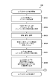
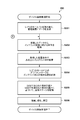
- the figure which shows the structure of the imprint system which concerns on embodiment. 6 is a flowchart for explaining a control operation of the imprint system according to the embodiment. 6 is a flowchart for explaining a control operation of the imprint system according to the embodiment. 6 is a flowchart for explaining a control operation of the imprint system according to the embodiment.
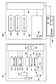
- FIG. 1 is a diagram illustrating a configuration of an imprint system according to the present embodiment.
- the imprint system can include a replica manufacturing apparatus 100, an imprint apparatus 200, and a management apparatus 300.
- the management apparatus 300 is communicably connected to the replica manufacturing apparatus 100 and the imprint apparatus 200.
- the imprint apparatus 200 is an apparatus that forms a cured product pattern to which a concave / convex pattern of a mold is transferred by bringing the imprint material supplied on the substrate into contact with the mold and applying energy for curing to the imprint material. It is.
- a curable composition (which may be referred to as an uncured resin) that is cured by being given energy for curing is used.
- energy for curing electromagnetic waves, heat, or the like can be used.
- the electromagnetic wave can be, for example, light having a wavelength selected from a range of 10 nm to 1 mm, for example, infrared rays, visible rays, ultraviolet rays, and the like.
- the curable composition may be a composition that is cured by light irradiation or by heating.
- the photocurable composition that is cured by light irradiation contains at least a polymerizable compound and a photopolymerization initiator, and may further contain a non-polymerizable compound or a solvent as necessary.
- the non-polymerizable compound is at least one selected from the group consisting of a sensitizer, a hydrogen donor, an internal release agent, a surfactant, an antioxidant, and a polymer component.
- the imprint material can be supplied onto the substrate in the form of droplets or an island or film formed by connecting a plurality of droplets by an imprint material supply device.
- the viscosity of the imprint material can be, for example, 1 mPa ⁇ s or more and 100 mPa ⁇ s or less.
- the material of the substrate for example, glass, ceramics, metal, semiconductor, resin, or the like can be used. If necessary, a member made of a material different from the substrate may be provided on the surface of the substrate.
- the substrate is, for example, a silicon substrate, a compound semiconductor substrate, or quartz glass.
- the imprint apparatus 200 employs a photocuring method that cures the imprint material by irradiation with ultraviolet rays, but is not limited to this, for example, thermal curing that cures the imprint material by heat input.
- a photocuring method that cures the imprint material by irradiation with ultraviolet rays
- thermal curing that cures the imprint material by heat input.
- the law can also be adopted.
- the substrate stage 220 is configured to be movable while holding the substrate 40.
- the dispenser 230 constituting the above-described imprint material supply apparatus supplies (arranges) the imprint material 231 on the substrate 40 held on the substrate stage 220.
- the imprint head 210 may include a driving mechanism for holding the mold 30 and bringing the mold 30 into contact with the imprint material 231 on the substrate 40.
- a curing unit 24 that irradiates the imprint material 231 on the substrate 40 through the mold 30 to cure the imprint material 231 includes a light source unit 240, a wavelength selection unit 241, a light reduction unit 242, a slit mechanism 243, and A light amount measurement unit 244 may be included.
- the light source unit 240 includes a light source that generates ultraviolet rays for curing the imprint material 231.
- As the light source for example, a high-pressure mercury lamp, a xenon lamp, an excimer laser, or the like can be used.
- the wavelength selection unit 241 can include, for example, a plurality of wavelength filters that transmit light having different wavelengths, and a mechanism that inserts or removes any one of the plurality of wavelength filters into the optical path.
- the dimming unit 242 can include, for example, a plurality of ND filters and a mechanism for inserting or removing any ND filter selected from the plurality of ND filters onto the optical path.
- the slit mechanism 243 can include, for example, a light shielding blade that defines the shape of the illumination area and a drive mechanism that drives the oblique light blade.
- the light quantity measurement unit 244 includes, for example, a UC sensor, and can measure the light quantity of light emitted from the light source unit 240.
- the alignment scope 232 is a microscope for aligning the mold 30 and the substrate 40 after the imprint material 231 is placed on the substrate 40 by the dispenser 230. By aligning the alignment state of the alignment mark 31 provided on the mold 30 and the alignment mark 41 provided on the substrate 40 with the alignment scope 232, mutual alignment is performed.
- the alignment scope 232 can also acquire information on the relative displacement between the alignment mark 31 provided on the mold 30 and the imprint material 231 disposed on the substrate 40.
- identification information is formed in the mold 30 and can be read by the reading unit 251.
- the imprint apparatus 200 may include an imaging unit 221 for observing the state when the mold 30 is brought into contact with the imprint material 231 on the substrate 40 and when the mold is released. In FIG.
- the image pickup unit 221 is provided on the substrate stage 220 side and picks up images from the back side of the substrate. Conversely, the image pickup unit 221 is provided on the imprint head 210 side and picks up images from the front side of the mold. You may make it do.
- the control unit 260 includes, for example, a CPU 261 and a memory 262, and controls each unit of the imprint apparatus 200.
- the control unit 260 performs imprint processing as follows. First, the imprint material 231 is disposed on the substrate 40 by the dispenser 230. Thereafter, the mold 30 is lowered by the imprint head 210 and brought into contact with the imprint material 231 on the substrate 40. As a result, the imprint material 231 flows into the groove of the pattern formed in the mold 30. In this state, the imprint material 231 is cured by irradiating the imprint material 231 with ultraviolet rays by the curing unit 24.
- the imprint material 231 When the imprint material 231 is cured, a pattern (circuit pattern) of the mold 30 is formed by the imprint material 231. After the imprint material 231 is cured, the mold 30 is lifted by the imprint head 210, whereby the mold 30 is separated from the cured imprint material 231 (release).
- the imprint process in this embodiment is generally as described above.
- the imprint head 210 is driven and brought into contact with the imprint material 231 on the fixed substrate 40.
- the substrate stage 220 may be driven with respect to the fixed mold 30 so that the imprint material 231 on the substrate 40 is brought into contact therewith.
- the structure which drives the imprint head 210 and the substrate stage 220 up and down may be sufficient. That is, it is only necessary to have a drive unit that changes the relative positions of the mold 30 and the substrate 40.
- the replica manufacturing apparatus 100 is an apparatus for manufacturing such a replica mold.
- the basic configuration of the replica manufacturing apparatus 100 is substantially the same as that of the imprint apparatus 200.
- the substrate stage 120 is configured to be movable while holding the replica substrate 20.
- the dispenser 130 arranges the imprint material 131 on the replica substrate 20 held on the substrate stage 120.
- the imprint head 110 can include a driving mechanism for holding the mold 10 as a master mold and bringing the mold 10 into contact with the imprint material 131 on the replica substrate 20.
- the curing unit 14 cures the imprint material 131 on the replica substrate 20.
- the curing unit 14 that irradiates the imprint material 131 on the replica substrate 20 through the mold 10 to cure the imprint material 131 includes a light source unit 140, a wavelength selection unit 141, a light reduction unit 142, a slit mechanism 143, And a light amount measurement unit 144.
- the light source unit 140 includes a light source that generates ultraviolet rays for curing the imprint material 131.
- a high-pressure mercury lamp, a xenon lamp, an excimer laser, or the like can be used.
- the wavelength selection unit 141 includes a plurality of wavelength filters that transmit light having different wavelengths, and a mechanism that arranges a wavelength filter selected from the plurality of wavelength filters on an optical path between the light source and the mold. May be included.
- the dimming unit 142 can include, for example, a plurality of ND filters and a mechanism for inserting or removing any ND filter selected from the plurality of ND filters into the optical path.
- the slit mechanism 143 can include, for example, a light shielding blade that defines the shape of the illumination area and a drive mechanism that drives the oblique light blade.
- the light quantity measurement unit 144 includes, for example, a UC sensor, and can measure the light quantity of light emitted from the light source unit 140.
- the alignment scope 132 is a microscope for aligning the mold 10 and the replica substrate 20 after the imprint material 131 is placed on the replica substrate 20 by the dispenser 130. By aligning the alignment mark 11 provided on the mold 10 and the alignment mark 21 provided on the replica substrate 20 with the alignment scope 132, mutual alignment is performed.
- the alignment scope 132 can also acquire information on the relative displacement between the alignment mark 11 provided on the mold 10 and the imprint material 131 disposed on the replica substrate 20. Further, an ID is formed on the mold 10 and can be read by the reading unit 151.
- the replica manufacturing apparatus 100 can include an imaging unit 121 for observing the state when the mold 10 is brought into contact with the imprint material 131 on the replica substrate 20 and when the mold is released. In FIG. 1, the imaging unit 121 is provided on the substrate stage 120 side and images from the back side of the substrate. Conversely, the imaging unit 121 is provided on the imprint head 110 side and images from the front side of the mold. May do
- the control unit 160 includes, for example, a CPU 161 and a memory 162, and controls each unit of the replica manufacturing apparatus 100.
- the control unit 160 controls the production of the replica mold by a process similar to the imprint process performed by the imprint apparatus 200 described above. Specifically, first, the imprint material 131 is placed on the replica substrate 20 by the dispenser 130. Thereafter, the mold 10 as a master mold is lowered by the imprint head 110 and brought into contact with the imprint material 131 on the replica substrate 20. As a result, the imprint material 131 flows into the groove of the pattern formed in the mold 10. In this state, the imprint material 131 is cured by irradiating the imprint material 131 with ultraviolet rays by the curing unit 14.
- a pattern (circuit pattern) of the mold 10 is formed by the imprint material 131.
- the mold 10 is lifted by the imprint head 110, whereby the mold 10 is separated from the cured imprint material 131 (release).
- the imprint head 110 is driven and brought into contact with the imprint material 131 on the fixed replica substrate 20, but there is a configuration opposite to this. sell. That is, the imprint material 131 on the replica substrate 20 may be brought into contact with the fixed mold 10 by driving the substrate stage 120. Alternatively, the imprint head 110 and the substrate stage 120 may be driven up and down. That is, it is only necessary to have a drive unit that changes the relative position between the mold 10 and the replica substrate 20.
- the replica substrate 20 on which the circuit pattern is formed by the imprint material 131 is completed as a replica mold having an uneven circuit pattern through an etching process in a later step.
- a pattern is formed by a known inversion process, as a result, a circuit pattern similar to that of the mold 10 as a master mold is formed in the replica mold.
- the conditions relating to the imprint process can be optimized according to the circuit pattern to be manufactured.
- the control unit 160 selects these conditions according to the circuit pattern to be manufactured, and controls the imprint process so that the circuit pattern is formed on the replica substrate 20.
- the imprint apparatus 200 can use the replica mold thus manufactured as the mold 30. As described above, when a pattern is formed by an inversion process, a circuit pattern similar to that of the mold 10 that is a master mold is formed on the mold 30 that is a replica mold.
- the conditions related to the imprint process for the mold 30 that is a replica mold in the imprint apparatus 200 can be diverted to the conditions related to the imprint process in manufacturing the replica mold in the replica manufacturing apparatus 100.
- the conditions regarding imprint processing may include, for example, the following.
- Arrangement condition Information indicating the relationship between the arrangement position and the arrangement amount of the imprint material 131 on the replica substrate 20.
- the arrangement conditions are set based on the density of the circuit pattern of the mold 10 and the like so that unfilled defects are suppressed and the thickness of the imprint material on the substrate after the imprint process is constant.
- Contact condition information that defines the operation of the drive unit, such as the drive amount of the imprint head 110 when the mold 10 is brought into contact with the imprint material 131.
- Irradiation conditions curing conditions that define the operation of the curing unit 14, and information such as the amount of ultraviolet light irradiated from the light source unit 140 and the irradiation time.
- Mold release condition information that defines the operation of the drive unit, such as the drive amount of the imprint head 110 when the mold 10 is separated from the cured imprint material 131.
- the conditions regarding the imprint process may further include the following conditions regarding the curing unit 14.
- Wavelength selection condition wavelength filter selection information in the wavelength selection unit 141.
- Filter selection condition ND filter selection information in the dimming unit 142.
- Slit setting condition setting information regarding driving of the slit mechanism 143.
- the management apparatus 300 stores data including the above-described various conditions related to the imprint process at the time of replica mold manufacturing in the replica manufacturing apparatus 100, and stores this data in response to a request from the imprint apparatus 200. Forward to.
- the management apparatus 300 may also transfer the light quantity measurement result by the light quantity measurement unit 144 to the imprint apparatus 200. Thereby, the imprint apparatus 200 can adjust the selection conditions of the light reduction unit 242, the irradiation time by the light source unit 240, and the like.
- the management device 300 can be realized by a computer device including a CPU 301 and a memory 302, for example.
- FIG. 3 shows an example of the positional relationship between the mold 10, the replica substrate 20, and the imprint material 131 thereon when the replica mold is manufactured by the replica manufacturing apparatus 100.
- An alignment mark 11 and a circuit pattern 12 are formed on the mold 10.
- an imprint material 131 represented by a black circle is arranged by a dispenser 130 (first supply unit).
- the relative positions ⁇ X and ⁇ Y between the alignment mark 11 and the imprint material 131 disposed by the dispenser 130 are measured by the alignment scope 132 (first measurement unit).
- the relative positions ⁇ X and ⁇ Y measured here are relative position offsets.
- FIG. 3 shows an example of the positional relationship between the mold 30 (replica mold), the substrate 40, and the imprint material 231 thereon in the imprint apparatus 200.
- FIG. An alignment mark 31 corresponding to the alignment mark 11 of the mold 10 that is a master mold and a circuit pattern 32 corresponding to the circuit pattern 12 are formed on the mold 30. If the alignment mark 31 is a transfer of the alignment mark 11 of the mold 10 that is a master mold, the relative position between the alignment mark 31 and the circuit pattern 32 is the same as the relative position between the alignment mark 11 and the circuit pattern 12. .
- Relative positions ⁇ X and ⁇ Y between the alignment mark 31 and the imprint material 231 disposed by the dispenser 230 (second supply unit) are measured by the alignment scope 232 (second measurement unit). If the relative position measured here is different from the case of the replica manufacturing apparatus 100 shown in the left figure, the substrate stage 220 is driven so that the relative position becomes the relative position ⁇ X, ⁇ Y in the replica manufacturing apparatus 100 to drive the substrate 40. Move.
- the memory 162 of the control unit 160 stores preset conditions regarding imprint processing.
- the control unit 160 controls the dispenser 130 according to the arrangement conditions stored in the memory 162 to arrange the imprint material 131 on the replica substrate 20.
- the control unit 160 causes the alignment scope 132 to measure the relative position between the alignment mark 11 of the mold 10 and the imprint material 131 on the replica substrate 20.
- the measured relative position value is stored in the memory 162 as a relative position offset.
- the control unit 160 controls the imprint head 110 according to the contact condition stored in the memory 162 to bring the mold 10 into contact with the imprint material 131 on the replica substrate 20.
- the alignment of the mold 10 and the replica substrate 20 is also performed using the alignment scope 132.
- the control unit 160 cures the imprint material 131 by controlling the light source unit 140 according to the irradiation condition stored in the memory 162 and irradiating the imprint material 131 with light.
- the control unit 160 controls the imprint head 110 according to the mold release conditions stored in the memory 162 to perform mold release to pull the mold 10 away from the imprint material 131.
- the replica substrate 20 is processed into a replica mold in which the same circuit pattern as that of the mold 10 is formed by using an inversion process through a subsequent etching process.
- the control unit 160 uses the reading unit 151 to read the replica substrate ID 50 formed in advance on the replica substrate 20 as the replica mold ID.
- the control unit 160 transfers the data including the relative position offset and the conditions related to the imprint process to the management apparatus 300 in association with the replica mold ID.
- Conditions relating to the imprint process may include the above-described arrangement conditions, contact conditions, irradiation conditions, mold release conditions, waveform selection conditions, filter selection conditions, slit setting conditions, and the like.
- the management apparatus 300 stores the data received from the replica manufacturing apparatus 100 in the memory 302 (S301).
- the imprint apparatus 200 uses the replica mold manufactured by the replica manufacturing apparatus 100 as the mold 30 and executes imprint processing.
- the control unit 260 reads the replica mold ID 50 of the mold 30 held by the imprint head 210 using the reading unit 251. Thereafter, the control unit 260 issues request data including the read replica mold ID 50 to the management apparatus 300.
- the management apparatus 300 that has received the request data transmits data including an ID that matches the replica mold ID 50 included in the request data to the imprint apparatus 200 (S302).
- the imprint apparatus 200 receives this data, and acquires conditions relating to imprint processing (S202). These acquired conditions are stored in the memory 262.
- the control unit 260 controls the dispenser 230 according to the acquired arrangement condition, and arranges the imprint material 231 on the substrate 40.
- the control unit 260 causes the alignment scope 232 to measure the relative position between the alignment mark 31 of the mold 30 and the imprint material 231 on the substrate 40.
- the control unit 260 drives the substrate stage 220 based on the relative position obtained by this measurement and the relative position acquired in S202. For example, the control unit 260 drives the substrate stage 220 so that the distance between the relative position measured by the alignment scope 230 and the relative position acquired in S202 falls within an allowable range.
- the control unit 260 controls the imprint head 210 in accordance with the contact condition acquired in S202 and stored in the memory 262 to bring the mold 30 into contact with the imprint material 231 on the substrate 40.
- the alignment of the mold 30 and the substrate 40 is also performed using the alignment scope 232.
- the control unit 260 cures the imprint material 231 by controlling the curing unit 24 according to the irradiation condition acquired in S202 and stored in the memory 262 to irradiate the imprint material 231 with light.
- the control unit 260 controls the imprint head 210 according to the mold release condition acquired in S202 and stored in the memory 262, and performs the mold release for separating the mold 30 from the imprint material 231. Do.
- the conditions relating to the imprint processing at the time of manufacturing the replica mold in the replica manufacturing apparatus 100 are diverted as conditions relating to the imprint processing for the mold 30 which is a replica mold in the imprint apparatus 200.
- the circuit pattern when the circuit pattern is formed on the replica substrate 20 can be reproduced on the substrate 40 while suppressing unfilled defects.
- the alignment mark 11 of the master mold (mold 10) can be transferred to the replica substrate 20 simultaneously with the circuit pattern.
- the transferred mark of the alignment mark 11 of the master mold can be used as the alignment mark 31 of the replica mold (mold 30). Therefore, it is possible to match the placement position of the imprint material without causing a drawing error between the circuit pattern and the alignment mark.
- the arrangement conditions in the present embodiment can include not only the arrangement position of the imprint material on the substrate but also information on the arrangement amount of the imprint material as described above.
- information on the arrangement amount of the imprint material for each nozzle of the dispenser 130 is stored in the memory 162, and this information is notified to the imprint apparatus 200.
- the control unit 260 calculates a difference from the information on the arrangement amount of the imprint material for each nozzle of the dispenser 230 and corrects the arrangement amount. This makes it possible to match the amount of imprint material without considering the difference in the amount of imprint material between devices, and to reproduce the film thickness of the pattern formed on the substrate. Is possible.
- the arrangement amount of the imprint material can be corrected by the voltage value and the opening time when the imprint material is pushed out.
- the replica manufacturing apparatus 100 and the imprint apparatus 200 each have a unique offset
- the dispenser 130 of the replica manufacturing apparatus 100 and the dispenser 230 of the imprint apparatus 200 each have an attachment position offset
- an attachment position offset of the dispenser 230 of the imprint apparatus 200 is set to ⁇ X 230 .
- ⁇ X replica_ref ⁇ X m0 + ⁇ X 130
- ⁇ X ⁇ X m1 + ⁇ X 130
- the result ⁇ X offset obtained by removing the device-specific mounting offset ⁇ X 130 is obtained as in the following equation. .
- ⁇ X imprint_ref ⁇ X m0 + ⁇ X 230
- ⁇ X offset calculated by the replica manufacturing apparatus 100 is added to ⁇ X imprint_ref .
- the target position of ⁇ X in the imprint apparatus 200 of FIG. 3 is obtained considering only the pattern error ⁇ X m1 of the mold used in device manufacture and the mounting position offset ⁇ X 230 of the dispenser 230 of the imprint apparatus 200. Can do.
- ⁇ X has been described, but ⁇ Y can be corrected in the same manner, and thus the description thereof is omitted.
- the offset of the dispenser mounting position has been described as an example, but the present invention is not limited thereto.
- the replica manufacturing apparatus 100 places the imprint material 131 on the replica substrate 20, and then contacts the mold 10, which is a master mold, with the imprint material 131. At this time, the replica manufacturing apparatus 100 deforms the pattern surface of the mold 10 so as to be convex toward the replica substrate 20, and then makes contact with the imprint material 131 on the replica substrate 20. Then, the pattern surface 10a of the mold 10 comes into contact with the imprint material 131 from the center to the outside. Thereby, it is suppressed that air bubbles are confined between the mold 10 and the imprint material 131.
- the pattern of the imprint material formed on the replica substrate 20 is lost by gradually peeling from the imprint material 131 from the outside of the pattern surface of the mold 10 toward the center. Can be prevented.
- the state at this time is imaged by the imaging unit 121.
- the replica manufacturing apparatus 100 manages management data including the replica board ID 50 and the measurement result (control profile) of the contact state between the mold 10 and the imprint material 131 based on the image captured by the imaging unit 121. Transfer to device 300.
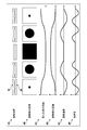
- Fig. 4 shows a conceptual diagram of the contact state.
- the contact state 4A indicates a state transition until the mold 10 is brought into contact with the imprint material 131 on the replica substrate 20 while being deformed as described above, and thereafter the mold release is performed.
- the contact portion image 4B is a state of a portion where the mold 10 and the replica substrate 20 are in contact with each other via the imprint material 131 according to the state transition 4A, which is measured based on the image captured by the imaging unit 121. It is an image which shows a transition.
- the distance 4C between the mold and the substrate indicates a change in the position of the mold 10 (distance between the mold 10 and the replica substrate 20) by the imprint head 110 according to the state transition 4A.
- the area 4D of the contact portion indicates a change in the area of the portion where the mold 10 and the replica substrate 20 are in contact via the imprint material 131 accompanying the state transition of the image 4B of the contact portion.
- the contact speed 4E indicates a change in the moving speed of the mold 10 by the imprint head 110 according to the state transition of the distance 4C between the mold and the substrate.
- the acceleration 4F indicates a change in the movement acceleration of the mold 10 by the imprint head 110 in accordance with the state transition of the distance 4C between the mold and the substrate.
- the control profile included in the management data may be the image 4B of the contact portion itself or the value of the area 4D of the contact portion.
- the imaging unit 221 causes the mold 30 to come into contact with the imprint material 231 disposed on the substrate 40, and a contact state when performing mold release is observed.
- the imprint apparatus 200 reads the ID 50 formed on the mold 30 by the reading unit 251, and acquires a control profile as a condition related to the imprint process according to the read ID from the management apparatus 300. Thereafter, in the imprint apparatus 200 as well, the pattern surface of the mold 30 comes into contact with the imprint material 231 from the center to the outside. Therefore, air bubbles are prevented from being trapped between the mold 30 and the imprint material 231.
- the pattern surface of the mold 30 is gradually peeled from the imprint material 231 from the outside toward the center, so that the imprint material pattern formed on the substrate 40 is not damaged. Can be prevented.
- the state at this time is imaged by the imaging unit 221. Data of the imaged result is compared with management data (corresponding to the contact portion image 4B or the contact portion area 4D) stored in the management device 300. If they are different as a result of the comparison, the driving speed of the driving unit (for example, the imprint head 210) that changes the deformation amount of the mold 30 or the relative position between the mold 30 and the substrate 40 is corrected. Thereby, it is possible to reproduce the mold contact, the release state, and the defect suppression accuracy in the imprint process when the replica substrate is manufactured in the imprint process during device manufacture.
- condition regarding the imprint process described above may be information on the distance 4C, the speed 4E, and / or the acceleration 4F instead of the information on the contact state.
- the condition relating to the imprint process may be information on the driving force of the driving unit.
- the thrust of the drive shaft of the imprint head 110 at the time of contact and release for example, the current value of the actuator is monitored and stored in the memory 162 of the control unit 160 and notified to the control unit 260.
- the imprint head 210 can feed back the notified current value to the driving thrust, and the stress applied to the pattern portion of the mold can be made uniform during replica mold manufacturing and device manufacturing.
- the contact and mold release conditions optimized at the time of replica mold manufacture can be easily reproduced at the time of device manufacture.
- the condition related to the imprint process may be information on the posture of the mold.
- a displacement meter that measures the inclination and gap of the surface of the substrate is provided.
- the inclination is stored in the memory 162 of the control unit 160 and notified to the control unit 260.
- the notified tilt information is fed back when the device is manufactured.
- the posture can be adjusted in contact and mold release at the time of replica mold manufacture and device manufacture.
- FIG. 5 is a diagram illustrating a configuration of an imprint system having a cluster configuration.
- the configurations of the replica manufacturing apparatus 100 and the management apparatus 300 are the same as those in FIG. 5 includes a cluster apparatus 400 including a plurality of imprint units having the same configuration as the imprint apparatus 200 of FIG.
- the cluster apparatus 400 includes a plurality of imprint units including a first imprint unit 471, a second imprint unit 472, and a third imprint unit 473, a reading unit 451 for reading a mold ID, a transport mechanism 480, and a control Part 460.
- the first imprint unit 471, the second imprint unit 472, and the third imprint unit 473 each have the same configuration as the imprint apparatus 200 of FIG.
- the transport mechanism 480 transports the mold carried into the cluster device 400 to the imprint unit designated by the control unit 460.
- the management apparatus 300 can distribute data including conditions regarding imprint processing to each imprint apparatus. Specifically, when a mold (replica template) is loaded into the cluster apparatus 400, the control unit 460 reads the mold ID by the reading unit 451. The control unit 460 requests the management device 300 for data corresponding to the read ID, and receives data from the management device 300. The control unit 460 controls the transport mechanism 480 to transport the replica mold to the target imprint unit, and transmits the received data to the imprint unit. Each imprint unit executes imprint processing according to the received data, as described above. Thereby, in each imprint part, the circuit pattern when the circuit pattern is formed on the replica substrate by the replica manufacturing apparatus 100 can be reproduced on the device substrate.
- the reference is matched between the replica manufacturing apparatus 100 and each imprint unit in advance using a reference mold as described above. The difference between the devices can be canceled.
- the pattern of the cured product formed using the imprint apparatus is used permanently on at least a part of various articles or temporarily used when manufacturing various articles.
- the article is an electric circuit element, an optical element, a MEMS, a recording element, a sensor, or a mold.
- the electric circuit elements include volatile or nonvolatile semiconductor memories such as DRAM, SRAM, flash memory, and MRAM, and semiconductor elements such as LSI, CCD, image sensor, and FPGA.
- Examples of the mold include an imprint mold.
- the pattern of the cured product is used as it is as at least a part of the above-mentioned article or temporarily used as a resist mask. After etching or ion implantation or the like is performed in the substrate processing step, the resist mask is removed.
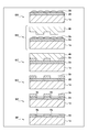
- step SA a substrate 1z such as a silicon substrate on which a workpiece 2z such as an insulator is formed is prepared, and then an imprint material 3z is applied to the surface of the workpiece 2z by an inkjet method or the like. .
- a state is shown in which the imprint material 3z in the form of a plurality of droplets is applied on the substrate.
- step SB the imprint mold 4z is opposed to the imprint material 3z on the substrate with the side having the concave / convex pattern formed thereon.
- step SC the substrate 1 provided with the imprint material 3z is brought into contact with the mold 4z, and pressure is applied.
- the imprint material 3z is filled in a gap between the mold 4z and the workpiece 2z. In this state, when light is irradiated as energy for curing through the mold 4z, the imprint material 3z is cured.
- step SD after the imprint material 3z is cured, when the mold 4z and the substrate 1z are separated, a pattern of a cured product of the imprint material 3z is formed on the substrate 1z.
- This cured product pattern has a shape in which the concave portion of the mold corresponds to the convex portion of the cured product, and the convex portion of the mold corresponds to the concave portion of the cured product. It will be done.
- step SE when the pattern of the cured product is etched using an etching resistant pattern, the portion of the surface of the workpiece 2z where there is no cured product or remains thin is removed, and the groove 5z is formed.
- the pattern of the cured product is removed in step SF, an article in which the groove 5z is formed on the surface of the workpiece 2z can be obtained.
- the cured product pattern is removed here, it may be used as, for example, a film for interlayer insulation contained in a semiconductor element or the like, that is, a constituent member of an article without being removed after processing.
- the present invention supplies a program that realizes one or more functions of the above-described embodiments to a system or apparatus via a network or a storage medium, and one or more processors in a computer of the system or apparatus read and execute the program This process can be realized. It can also be realized by a circuit (for example, ASIC) that realizes one or more functions.
- a circuit for example, ASIC
Landscapes
- Engineering & Computer Science (AREA)
- Physics & Mathematics (AREA)
- General Physics & Mathematics (AREA)
- Mechanical Engineering (AREA)
- Manufacturing & Machinery (AREA)
- Condensed Matter Physics & Semiconductors (AREA)
- Computer Hardware Design (AREA)
- Microelectronics & Electronic Packaging (AREA)
- Power Engineering (AREA)
- Shaping Of Tube Ends By Bending Or Straightening (AREA)
- Exposure Of Semiconductors, Excluding Electron Or Ion Beam Exposure (AREA)
Priority Applications (2)
| Application Number | Priority Date | Filing Date | Title |
|---|---|---|---|
| KR1020197019699A KR102204105B1 (ko) | 2016-12-09 | 2017-11-27 | 임프린트 시스템 및 물품 제조 방법 |
| US16/432,173 US11235495B2 (en) | 2016-12-09 | 2019-06-05 | Imprint system and article manufacturing meihod |
Applications Claiming Priority (2)
| Application Number | Priority Date | Filing Date | Title |
|---|---|---|---|
| JP2016-239776 | 2016-12-09 | ||
| JP2016239776A JP6755168B2 (ja) | 2016-12-09 | 2016-12-09 | インプリントシステム、レプリカ製造装置、管理装置、インプリント装置、および物品製造方法 |
Related Child Applications (1)
| Application Number | Title | Priority Date | Filing Date |
|---|---|---|---|
| US16/432,173 Continuation US11235495B2 (en) | 2016-12-09 | 2019-06-05 | Imprint system and article manufacturing meihod |
Publications (1)
| Publication Number | Publication Date |
|---|---|
| WO2018105418A1 true WO2018105418A1 (ja) | 2018-06-14 |
Family
ID=62491148
Family Applications (1)
| Application Number | Title | Priority Date | Filing Date |
|---|---|---|---|
| PCT/JP2017/042311 Ceased WO2018105418A1 (ja) | 2016-12-09 | 2017-11-27 | インプリントシステム、および物品製造方法 |
Country Status (5)
| Country | Link |
|---|---|
| US (1) | US11235495B2 (enExample) |
| JP (1) | JP6755168B2 (enExample) |
| KR (1) | KR102204105B1 (enExample) |
| TW (1) | TWI641027B (enExample) |
| WO (1) | WO2018105418A1 (enExample) |
Families Citing this family (3)
| Publication number | Priority date | Publication date | Assignee | Title |
|---|---|---|---|---|
| PL3650224T3 (pl) * | 2018-11-09 | 2023-09-18 | Phoenix Contact Gmbh & Co. Kg | Urządzenie i sposób zadrukowywania artykułu |
| JP7190942B2 (ja) * | 2019-03-08 | 2022-12-16 | キヤノン株式会社 | インプリントシステム、管理装置、および物品製造方法 |
| JP2022142518A (ja) | 2021-03-16 | 2022-09-30 | キオクシア株式会社 | テンプレート、マーク、及びテンプレートの製造方法 |
Citations (3)
| Publication number | Priority date | Publication date | Assignee | Title |
|---|---|---|---|---|
| JP2012234901A (ja) * | 2011-04-28 | 2012-11-29 | Toshiba Corp | インプリント装置の動作方法及びインプリント用テンプレートの管理装置の動作方法 |
| JP2016092270A (ja) * | 2014-11-06 | 2016-05-23 | キヤノン株式会社 | インプリントシステム及び物品の製造方法 |
| JP2016178127A (ja) * | 2015-03-18 | 2016-10-06 | キヤノン株式会社 | インプリントシステム、および物品の製造方法 |
Family Cites Families (10)
| Publication number | Priority date | Publication date | Assignee | Title |
|---|---|---|---|---|
| US736085A (en) | 1902-10-15 | 1903-08-11 | Carroll W Kjelgaard | Combination shade and curtain bracket. |
| US7360851B1 (en) | 2006-02-15 | 2008-04-22 | Kla-Tencor Technologies Corporation | Automated pattern recognition of imprint technology |
| JP2010052175A (ja) | 2008-08-26 | 2010-03-11 | Fuji Electric Device Technology Co Ltd | ナノインプリント用マスターモールドの製造方法およびレプリカモールドの製造方法 |
| EP2256549A1 (en) | 2009-05-29 | 2010-12-01 | Obducat AB | Fabrication of Metallic Stamps for Replication Technology |
| JP2012190877A (ja) | 2011-03-09 | 2012-10-04 | Fujifilm Corp | ナノインプリント方法およびそれに用いられるナノインプリント装置 |
| JP6053266B2 (ja) * | 2011-09-01 | 2016-12-27 | キヤノン株式会社 | インプリント装置、物品の製造方法及びインプリント方法 |
| JP2013074115A (ja) * | 2011-09-28 | 2013-04-22 | Fujifilm Corp | ナノインプリント装置およびナノインプリント方法、並びに、歪み付与デバイスおよび歪み付与方法 |
| JP5935385B2 (ja) | 2012-02-27 | 2016-06-15 | 大日本印刷株式会社 | ナノインプリント用レプリカテンプレートの製造方法及びレプリカテンプレート |
| JP5942551B2 (ja) | 2012-04-03 | 2016-06-29 | 大日本印刷株式会社 | ナノインプリント用マスターテンプレート及びレプリカテンプレートの製造方法 |
| JP6138189B2 (ja) | 2015-04-08 | 2017-05-31 | キヤノン株式会社 | インプリント装置および物品の製造方法 |
-
2016
- 2016-12-09 JP JP2016239776A patent/JP6755168B2/ja active Active
-
2017
- 2017-11-27 WO PCT/JP2017/042311 patent/WO2018105418A1/ja not_active Ceased
- 2017-11-27 KR KR1020197019699A patent/KR102204105B1/ko active Active
- 2017-12-05 TW TW106142506A patent/TWI641027B/zh active
-
2019
- 2019-06-05 US US16/432,173 patent/US11235495B2/en active Active
Patent Citations (3)
| Publication number | Priority date | Publication date | Assignee | Title |
|---|---|---|---|---|
| JP2012234901A (ja) * | 2011-04-28 | 2012-11-29 | Toshiba Corp | インプリント装置の動作方法及びインプリント用テンプレートの管理装置の動作方法 |
| JP2016092270A (ja) * | 2014-11-06 | 2016-05-23 | キヤノン株式会社 | インプリントシステム及び物品の製造方法 |
| JP2016178127A (ja) * | 2015-03-18 | 2016-10-06 | キヤノン株式会社 | インプリントシステム、および物品の製造方法 |
Also Published As
| Publication number | Publication date |
|---|---|
| KR20190089213A (ko) | 2019-07-30 |
| JP6755168B2 (ja) | 2020-09-16 |
| KR102204105B1 (ko) | 2021-01-18 |
| US20190283281A1 (en) | 2019-09-19 |
| TWI641027B (zh) | 2018-11-11 |
| US11235495B2 (en) | 2022-02-01 |
| JP2018098306A (ja) | 2018-06-21 |
| TW201822251A (zh) | 2018-06-16 |
Similar Documents
| Publication | Publication Date | Title |
|---|---|---|
| US11841616B2 (en) | Imprint apparatus, imprint method, and method of manufacturing article | |
| JP7171468B2 (ja) | 情報処理装置、プログラム、リソグラフィ装置、物品の製造方法、物品の製造システム、及び出力方法 | |
| JP2018041774A (ja) | インプリント装置および物品製造方法 | |
| KR20180116747A (ko) | 임프린트 장치 및 물품 제조 방법 | |
| KR102293478B1 (ko) | 임프린트 장치 및 물품의 제조 방법 | |
| WO2018105418A1 (ja) | インプリントシステム、および物品製造方法 | |
| JP7603395B2 (ja) | インプリント装置、および物品の製造方法 | |
| KR20180107725A (ko) | 리소그래피 장치 및 물품의 제조 방법 | |
| JP2018073989A (ja) | インプリント方法、インプリント装置および物品製造方法 | |
| KR102286380B1 (ko) | 임프린트 장치, 임프린트 방법 및 물품의 제조 방법 | |
| JP7451141B2 (ja) | インプリント装置、インプリント方法、および物品の製造方法 | |
| JP2021176200A (ja) | インプリント装置および物品製造方法 | |
| KR20200077443A (ko) | 임프린트 장치 및 물품 제조 방법 | |
| JP2019021875A (ja) | インプリント方法、インプリント装置、および物品の製造方法 | |
| JP2023156163A (ja) | インプリント装置、インプリント方法及び物品の製造方法 | |
| JP7148284B2 (ja) | インプリント装置及び物品の製造方法 | |
| KR102898963B1 (ko) | 임프린트 장치, 임프린트 방법 및, 물품의 제조 방법 | |
| JP7421278B2 (ja) | インプリント装置、および物品製造方法 | |
| JP2021044339A (ja) | モールド、インプリント装置、物品の製造方法、インプリント方法 | |
| JP7441037B2 (ja) | インプリント装置、情報処理装置、インプリント方法及び物品の製造方法 | |
| JP2024176404A (ja) | インプリント装置、インプリント方法および物品製造方法 | |
| JP6742177B2 (ja) | インプリント装置、および物品製造方法 | |
| JP2025089783A (ja) | インプリント装置、インプリント方法、物品の製造方法、及びプログラム | |
| JP2024090241A (ja) | インプリント方法、インプリント装置、および物品の製造方法 | |
| JP2023058321A (ja) | インプリント装置及び物品の製造方法 |
Legal Events
| Date | Code | Title | Description |
|---|---|---|---|
| 121 | Ep: the epo has been informed by wipo that ep was designated in this application |
Ref document number: 17879600 Country of ref document: EP Kind code of ref document: A1 |
|
| NENP | Non-entry into the national phase |
Ref country code: DE |
|
| ENP | Entry into the national phase |
Ref document number: 20197019699 Country of ref document: KR Kind code of ref document: A |
|
| 122 | Ep: pct application non-entry in european phase |
Ref document number: 17879600 Country of ref document: EP Kind code of ref document: A1 |