WO2018092883A1 - 実装ヘッド - Google Patents
実装ヘッド Download PDFInfo
- Publication number
- WO2018092883A1 WO2018092883A1 PCT/JP2017/041484 JP2017041484W WO2018092883A1 WO 2018092883 A1 WO2018092883 A1 WO 2018092883A1 JP 2017041484 W JP2017041484 W JP 2017041484W WO 2018092883 A1 WO2018092883 A1 WO 2018092883A1
- Authority
- WO
- WIPO (PCT)
- Prior art keywords
- gas
- mounting head
- main body
- attachment
- suction
- Prior art date
- Legal status (The legal status is an assumption and is not a legal conclusion. Google has not performed a legal analysis and makes no representation as to the accuracy of the status listed.)
- Ceased
Links
Images










Classifications
-
- B—PERFORMING OPERATIONS; TRANSPORTING
- B23—MACHINE TOOLS; METAL-WORKING NOT OTHERWISE PROVIDED FOR
- B23K—SOLDERING OR UNSOLDERING; WELDING; CLADDING OR PLATING BY SOLDERING OR WELDING; CUTTING BY APPLYING HEAT LOCALLY, e.g. FLAME CUTTING; WORKING BY LASER BEAM
- B23K3/00—Tools, devices or special appurtenances for soldering, e.g. brazing, or unsoldering, not specially adapted for particular methods
- B23K3/08—Auxiliary devices therefor
- B23K3/087—Soldering or brazing jigs, fixtures or clamping means
-
- H—ELECTRICITY
- H05—ELECTRIC TECHNIQUES NOT OTHERWISE PROVIDED FOR
- H05K—PRINTED CIRCUITS; CASINGS OR CONSTRUCTIONAL DETAILS OF ELECTRIC APPARATUS; MANUFACTURE OF ASSEMBLAGES OF ELECTRICAL COMPONENTS
- H05K13/00—Apparatus or processes specially adapted for manufacturing or adjusting assemblages of electric components
- H05K13/04—Mounting of components, e.g. of leadless components
- H05K13/0404—Pick-and-place heads or apparatus, e.g. with jaws
- H05K13/0408—Incorporating a pick-up tool
- H05K13/0409—Sucking devices
-
- B—PERFORMING OPERATIONS; TRANSPORTING
- B23—MACHINE TOOLS; METAL-WORKING NOT OTHERWISE PROVIDED FOR
- B23K—SOLDERING OR UNSOLDERING; WELDING; CLADDING OR PLATING BY SOLDERING OR WELDING; CUTTING BY APPLYING HEAT LOCALLY, e.g. FLAME CUTTING; WORKING BY LASER BEAM
- B23K1/00—Soldering, e.g. brazing, or unsoldering
- B23K1/0008—Soldering, e.g. brazing, or unsoldering specially adapted for particular articles or work
- B23K1/0016—Soldering of electronic components
-
- H—ELECTRICITY
- H05—ELECTRIC TECHNIQUES NOT OTHERWISE PROVIDED FOR
- H05K—PRINTED CIRCUITS; CASINGS OR CONSTRUCTIONAL DETAILS OF ELECTRIC APPARATUS; MANUFACTURE OF ASSEMBLAGES OF ELECTRICAL COMPONENTS
- H05K13/00—Apparatus or processes specially adapted for manufacturing or adjusting assemblages of electric components
- H05K13/04—Mounting of components, e.g. of leadless components
-
- H—ELECTRICITY
- H10—SEMICONDUCTOR DEVICES; ELECTRIC SOLID-STATE DEVICES NOT OTHERWISE PROVIDED FOR
- H10W—GENERIC PACKAGES, INTERCONNECTIONS, CONNECTORS OR OTHER CONSTRUCTIONAL DETAILS OF DEVICES COVERED BY CLASS H10
- H10W72/00—Interconnections or connectors in packages
- H10W72/071—Connecting or disconnecting
- H10W72/072—Connecting or disconnecting of bump connectors
-
- H—ELECTRICITY
- H10—SEMICONDUCTOR DEVICES; ELECTRIC SOLID-STATE DEVICES NOT OTHERWISE PROVIDED FOR
- H10W—GENERIC PACKAGES, INTERCONNECTIONS, CONNECTORS OR OTHER CONSTRUCTIONAL DETAILS OF DEVICES COVERED BY CLASS H10
- H10W90/00—Package configurations
-
- B—PERFORMING OPERATIONS; TRANSPORTING
- B23—MACHINE TOOLS; METAL-WORKING NOT OTHERWISE PROVIDED FOR
- B23K—SOLDERING OR UNSOLDERING; WELDING; CLADDING OR PLATING BY SOLDERING OR WELDING; CUTTING BY APPLYING HEAT LOCALLY, e.g. FLAME CUTTING; WORKING BY LASER BEAM
- B23K2101/00—Articles made by soldering, welding or cutting
- B23K2101/36—Electric or electronic devices
- B23K2101/40—Semiconductor devices
-
- H—ELECTRICITY
- H10—SEMICONDUCTOR DEVICES; ELECTRIC SOLID-STATE DEVICES NOT OTHERWISE PROVIDED FOR
- H10W—GENERIC PACKAGES, INTERCONNECTIONS, CONNECTORS OR OTHER CONSTRUCTIONAL DETAILS OF DEVICES COVERED BY CLASS H10
- H10W72/00—Interconnections or connectors in packages
- H10W72/071—Connecting or disconnecting
- H10W72/0711—Apparatus therefor
-
- H—ELECTRICITY
- H10—SEMICONDUCTOR DEVICES; ELECTRIC SOLID-STATE DEVICES NOT OTHERWISE PROVIDED FOR
- H10W—GENERIC PACKAGES, INTERCONNECTIONS, CONNECTORS OR OTHER CONSTRUCTIONAL DETAILS OF DEVICES COVERED BY CLASS H10
- H10W72/00—Interconnections or connectors in packages
- H10W72/071—Connecting or disconnecting
- H10W72/0711—Apparatus therefor
- H10W72/07125—Means for controlling the bonding environment, e.g. valves or vacuum pumps
-
- H—ELECTRICITY
- H10—SEMICONDUCTOR DEVICES; ELECTRIC SOLID-STATE DEVICES NOT OTHERWISE PROVIDED FOR
- H10W—GENERIC PACKAGES, INTERCONNECTIONS, CONNECTORS OR OTHER CONSTRUCTIONAL DETAILS OF DEVICES COVERED BY CLASS H10
- H10W72/00—Interconnections or connectors in packages
- H10W72/071—Connecting or disconnecting
- H10W72/0711—Apparatus therefor
- H10W72/07141—Means for applying energy, e.g. ovens or lasers
-
- H—ELECTRICITY
- H10—SEMICONDUCTOR DEVICES; ELECTRIC SOLID-STATE DEVICES NOT OTHERWISE PROVIDED FOR
- H10W—GENERIC PACKAGES, INTERCONNECTIONS, CONNECTORS OR OTHER CONSTRUCTIONAL DETAILS OF DEVICES COVERED BY CLASS H10
- H10W72/00—Interconnections or connectors in packages
- H10W72/071—Connecting or disconnecting
- H10W72/0711—Apparatus therefor
- H10W72/07178—Means for aligning
-
- H—ELECTRICITY
- H10—SEMICONDUCTOR DEVICES; ELECTRIC SOLID-STATE DEVICES NOT OTHERWISE PROVIDED FOR
- H10W—GENERIC PACKAGES, INTERCONNECTIONS, CONNECTORS OR OTHER CONSTRUCTIONAL DETAILS OF DEVICES COVERED BY CLASS H10
- H10W72/00—Interconnections or connectors in packages
- H10W72/071—Connecting or disconnecting
- H10W72/072—Connecting or disconnecting of bump connectors
- H10W72/07231—Techniques
- H10W72/07236—Soldering or alloying
-
- H—ELECTRICITY
- H10—SEMICONDUCTOR DEVICES; ELECTRIC SOLID-STATE DEVICES NOT OTHERWISE PROVIDED FOR
- H10W—GENERIC PACKAGES, INTERCONNECTIONS, CONNECTORS OR OTHER CONSTRUCTIONAL DETAILS OF DEVICES COVERED BY CLASS H10
- H10W72/00—Interconnections or connectors in packages
- H10W72/071—Connecting or disconnecting
- H10W72/073—Connecting or disconnecting of die-attach connectors
-
- H—ELECTRICITY
- H10—SEMICONDUCTOR DEVICES; ELECTRIC SOLID-STATE DEVICES NOT OTHERWISE PROVIDED FOR
- H10W—GENERIC PACKAGES, INTERCONNECTIONS, CONNECTORS OR OTHER CONSTRUCTIONAL DETAILS OF DEVICES COVERED BY CLASS H10
- H10W72/00—Interconnections or connectors in packages
- H10W72/071—Connecting or disconnecting
- H10W72/073—Connecting or disconnecting of die-attach connectors
- H10W72/07331—Connecting techniques
- H10W72/07337—Connecting techniques using a polymer adhesive, e.g. an adhesive based on silicone or epoxy
-
- H—ELECTRICITY
- H10—SEMICONDUCTOR DEVICES; ELECTRIC SOLID-STATE DEVICES NOT OTHERWISE PROVIDED FOR
- H10W—GENERIC PACKAGES, INTERCONNECTIONS, CONNECTORS OR OTHER CONSTRUCTIONAL DETAILS OF DEVICES COVERED BY CLASS H10
- H10W72/00—Interconnections or connectors in packages
- H10W72/071—Connecting or disconnecting
- H10W72/073—Connecting or disconnecting of die-attach connectors
- H10W72/07331—Connecting techniques
- H10W72/07337—Connecting techniques using a polymer adhesive, e.g. an adhesive based on silicone or epoxy
- H10W72/07338—Connecting techniques using a polymer adhesive, e.g. an adhesive based on silicone or epoxy hardening the adhesive by curing, e.g. thermosetting
-
- H—ELECTRICITY
- H10—SEMICONDUCTOR DEVICES; ELECTRIC SOLID-STATE DEVICES NOT OTHERWISE PROVIDED FOR
- H10W—GENERIC PACKAGES, INTERCONNECTIONS, CONNECTORS OR OTHER CONSTRUCTIONAL DETAILS OF DEVICES COVERED BY CLASS H10
- H10W72/00—Interconnections or connectors in packages
- H10W72/20—Bump connectors, e.g. solder bumps or copper pillars; Dummy bumps; Thermal bumps
- H10W72/221—Structures or relative sizes
- H10W72/222—Multilayered bumps, e.g. a coating on top and side surfaces of a bump core
-
- H—ELECTRICITY
- H10—SEMICONDUCTOR DEVICES; ELECTRIC SOLID-STATE DEVICES NOT OTHERWISE PROVIDED FOR
- H10W—GENERIC PACKAGES, INTERCONNECTIONS, CONNECTORS OR OTHER CONSTRUCTIONAL DETAILS OF DEVICES COVERED BY CLASS H10
- H10W72/00—Interconnections or connectors in packages
- H10W72/20—Bump connectors, e.g. solder bumps or copper pillars; Dummy bumps; Thermal bumps
- H10W72/251—Materials
- H10W72/252—Materials comprising solid metals or solid metalloids, e.g. PbSn, Ag or Cu
-
- H—ELECTRICITY
- H10—SEMICONDUCTOR DEVICES; ELECTRIC SOLID-STATE DEVICES NOT OTHERWISE PROVIDED FOR
- H10W—GENERIC PACKAGES, INTERCONNECTIONS, CONNECTORS OR OTHER CONSTRUCTIONAL DETAILS OF DEVICES COVERED BY CLASS H10
- H10W72/00—Interconnections or connectors in packages
- H10W72/30—Die-attach connectors
- H10W72/351—Materials of die-attach connectors
- H10W72/353—Materials of die-attach connectors not comprising solid metals or solid metalloids, e.g. ceramics
- H10W72/354—Materials of die-attach connectors not comprising solid metals or solid metalloids, e.g. ceramics comprising polymers
-
- H—ELECTRICITY
- H10—SEMICONDUCTOR DEVICES; ELECTRIC SOLID-STATE DEVICES NOT OTHERWISE PROVIDED FOR
- H10W—GENERIC PACKAGES, INTERCONNECTIONS, CONNECTORS OR OTHER CONSTRUCTIONAL DETAILS OF DEVICES COVERED BY CLASS H10
- H10W74/00—Encapsulations, e.g. protective coatings
- H10W74/10—Encapsulations, e.g. protective coatings characterised by their shape or disposition
- H10W74/15—Encapsulations, e.g. protective coatings characterised by their shape or disposition on active surfaces of flip-chip devices, e.g. underfills
-
- H—ELECTRICITY
- H10—SEMICONDUCTOR DEVICES; ELECTRIC SOLID-STATE DEVICES NOT OTHERWISE PROVIDED FOR
- H10W—GENERIC PACKAGES, INTERCONNECTIONS, CONNECTORS OR OTHER CONSTRUCTIONAL DETAILS OF DEVICES COVERED BY CLASS H10
- H10W90/00—Package configurations
- H10W90/701—Package configurations characterised by the relative positions of pads or connectors relative to package parts
- H10W90/721—Package configurations characterised by the relative positions of pads or connectors relative to package parts of bump connectors
- H10W90/722—Package configurations characterised by the relative positions of pads or connectors relative to package parts of bump connectors between stacked chips
-
- H—ELECTRICITY
- H10—SEMICONDUCTOR DEVICES; ELECTRIC SOLID-STATE DEVICES NOT OTHERWISE PROVIDED FOR
- H10W—GENERIC PACKAGES, INTERCONNECTIONS, CONNECTORS OR OTHER CONSTRUCTIONAL DETAILS OF DEVICES COVERED BY CLASS H10
- H10W90/00—Package configurations
- H10W90/701—Package configurations characterised by the relative positions of pads or connectors relative to package parts
- H10W90/731—Package configurations characterised by the relative positions of pads or connectors relative to package parts of die-attach connectors
- H10W90/732—Package configurations characterised by the relative positions of pads or connectors relative to package parts of die-attach connectors between stacked chips
Definitions
- the present invention relates to a mounting head used in an electronic component mounting apparatus that joins an electrode of a semiconductor die and an electrode of a substrate or another semiconductor die.
- thermosetting resin a method in which a semiconductor die vacuum-adsorbed on an attachment is heated with a heat tool and pressed onto a substrate coated with a thermosetting resin to mount the semiconductor die on the substrate is often used.
- the thermosetting resin When the thermosetting resin is heated, the volatile component is gasified, and when the gasified volatile component is cooled, it is condensed to be liquid or solidified to be a solid. For this reason, the volatile component of the thermosetting resin gasified by heating is sucked into the vacuum flow path from the slight gap between the heat tool and the attachment or the slight gap between the attachment and the semiconductor die, and the inside of the switching valve.
- condensation or solidification may cause a vacuum suction operation failure, or solidification may occur in the gap between the heat tool and the attachment, resulting in a semiconductor die heating failure.
- the semiconductor die mounted in a stack has a protruding electrode on the surface that is attracted to the attachment, if the semiconductor die is vacuum-adsorbed to the tip of the attachment, it protrudes between the surface of the attachment and the surface of the semiconductor die. A gap is created by the height of the electrode. Since NCF gasifies components with low molecular weight such as acrylic monomer when heated to 200 ° C or higher, increasing the attachment temperature up to the melting temperature of the solder (about 250 ° C) causes NCF to gasify from this gap. The absorbed component is sucked into the vacuum suction hole inside the attachment.
- the temperature of the attachment it is necessary to cool the temperature of the attachment to, for example, about 100 ° C. so that the NCF does not become low viscosity.
- the pressure of the vacuum suction hole is vacuum, but after the semiconductor die is bonded, it is necessary to stop the vacuum in order to remove the semiconductor die from the attachment. For this reason, when the attachment is heated to about 250 ° C. when adsorbing the semiconductor die and bonding the electrodes, the gasification component of NCF is in a gas state in the vacuum suction hole provided inside the attachment. Sucked.
- the present invention has been made in view of the above circumstances, and an object thereof is to suppress the contamination of the mounting head.
- a mounting head is a mounting head used in an electronic component mounting apparatus that joins an electrode of a semiconductor die and a substrate or an electrode of another semiconductor die, and has an attachment surface that adsorbs the semiconductor die. And a bonding heater for heating the attachment and the semiconductor die, a main body for holding the bonding heater at an end surface, and a suction surface of the attachment. A first opening formed, a second opening formed on a surface different from the end surface of the main body, and a first flow path for bending the gas sucked from the first opening in the main body.
- the drip prevention unit is disposed on the downstream side of the suction direction of the gas with respect to the first bent portion of the suction path, and the droplet condensed with the gas or the solid solidified by the droplet. You may provide the storage part to store.
- the drip prevention unit may be provided immediately above a through hole that penetrates the bonding heater in the suction path, and may include a path heater that heats the gas to a temperature equal to or higher than the condensation temperature of the gas. Good.
- the drip prevention unit is disposed downstream of the first bent portion of the suction path in the gas suction direction, and a cooling unit that cools the gas to a temperature equal to or lower than the condensation temperature of the gas. You may prepare.
- the drip prevention unit may include a condensing unit that is disposed downstream of the first bent portion of the suction path in the gas suction direction and increases the fluid resistance of the gas.
- the suction path further includes a second bent portion provided downstream of the first bent portion in the gas suction direction, and the drip preventing portion includes the first bent portion and the first bent portion. Two bending portions may be provided.
- a storage unit that stores the droplets in which the gas is condensed or the solid in which the droplets are solidified may be disposed in the second bent portion.
- the main body may be configured to be vertically splitable on a split surface that passes through the storage portion that stores the droplets in which the gas is condensed or the solid in which the droplets are solidified.
- a bottom portion of the storage portion may be provided on a lower main body portion divided by the dividing surface.
- the main body includes a third opening in an upper main body divided by the dividing surface, and the third opening is tapered so as to gradually decrease toward the downstream side in the gas suction direction.
- the third opening may be configured such that a diameter of one end face of the third opening is larger than a diameter of the other end face on the downstream side in the suction direction of the third opening.
- the main body is disposed immediately above a through hole that penetrates the bonding heater in the suction path, and a path heater that heats the gas to a temperature equal to or higher than the condensation temperature of the gas; and the suction path A storage portion that is disposed downstream of the first bent portion of the gas in the gas suction direction and stores the liquid droplets condensed with the gas or a solid solidified by the liquid droplets, and the first bent portion of the suction path.
- a cooling unit that is disposed downstream of the gas suction direction and cools the gas to a temperature equal to or lower than the condensation temperature of the gas. The cooling unit may be sequentially provided along the gas suction direction.
- the main body has a protrusion at a position opposite to a position in the suction path where a reservoir for storing the liquid condensed the gas or a solid solidified from the liquid is provided. Further, it may be provided.
- the bonding heater and the main body may include materials having different thermal conductivities.
- the block diagram which shows the structure of the flip-chip bonding apparatus which concerns on embodiment of this invention The top view of the attachment used for the flip chip bonding apparatus which concerns on embodiment of this invention. Sectional drawing of the attachment used for the flip chip bonding apparatus which concerns on embodiment of this invention. The bottom view of the attachment used for the flip chip bonding apparatus which concerns on embodiment of this invention. The top view of the bonding heater used for the flip chip bonding apparatus which concerns on embodiment of this invention. Sectional drawing of the bonding heater used for the flip chip bonding apparatus which concerns on embodiment of this invention. The bottom view of the bonding heater used for the flip chip bonding apparatus which concerns on embodiment of this invention. The block diagram which shows the structure of the other flip chip bonding apparatus which concerns on embodiment of this invention.
- Sectional drawing seen from the VV direction of FIG. The block diagram which shows the structure of the other flip chip bonding apparatus which concerns on embodiment of this invention.
- Explanatory drawing which shows the state which adsorb
- the attachment is lowered to press the electrode of the second-stage semiconductor die against the electrode of the first-stage semiconductor die, and the second-stage semiconductor die is heated by the bonding heater FIG.
- FIG. 12 is a cross-sectional view seen from the XII-XII direction of FIG.
- the block diagram which shows an example of a structure of the main body used for the flip chip bonding apparatus which concerns on embodiment of this invention.
- FIG. 1 is a configuration diagram showing a configuration of a flip chip bonding apparatus according to an embodiment of the present invention.
- the flip-chip bonding apparatus 100 exemplarily includes a bonding stage 50 that attracts and fixes at least one of a semiconductor die 80 and a substrate 52 on the upper surface, and a vertical direction with respect to the bonding stage 50 by a driving device (not shown). And a mounting head 60 that is driven in a direction (vertical direction shown in FIG. 1) or a horizontal direction.
- the mounting head 60 is exemplarily disposed on the attachment 10 having the surface 14 (suction surface) for vacuum-sucking the semiconductor die 70 and the upper surface 18 opposite to the surface 14 of the attachment 10.
- the bonding heater 20 that heats the adsorbed semiconductor die 70, the main body 31 that holds the bonding heater 20 on the lower surface 33 (end surface), the first opening 19 that is formed on the surface 14 of the attachment 10, and the main body 31.
- the second opening 35 formed on a surface different from the lower surface 33 of the first and second bent portions 37 for bending the flow path of the gas sucked from the first opening 19 in the main body 31, and the attachment 10.
- a suction path as a through hole that penetrates the inside of the bonding heater 20 and the main body 31, and is sucked from the first opening 19.
- a suction path for example, a vacuum suction hole 16 formed in the attachment 10, a vacuum suction hole 22 formed in the bonding heater 20, and a vacuum formed in the main body 31.
- a drip prevention part 90 that is formed in the suction path and suppresses dripping of droplets condensed with gas onto the bonding heater 20.
- the main body 31 is connected to a driving device (not shown).
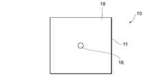
- FIG. 2A is a top view of the attachment used in the flip chip bonding apparatus according to the embodiment of the present invention.
- FIG. 2B is a cross-sectional view of an attachment used in the flip chip bonding apparatus according to the embodiment of the present invention.
- FIG. 2C is a bottom view of the attachment used in the flip chip bonding apparatus according to the embodiment of the present invention.
- the attachment 10 exemplarily has a square plate-like base 11 and a square pedestal projecting from the lower surface 12 of the base 11, and the semiconductor die 70 shown in FIG. And an island 13.
- a vacuum suction hole 16 for vacuum suction of the semiconductor die 70 is provided so as to penetrate the base 11 and the island 13.
- the bonding heater 20 is a square plate-like member in which a heating resistor made of platinum, tungsten, or the like is embedded in a ceramic such as aluminum nitride.
- the size of the bonding heater 20 is substantially the same as that of the attachment 10. Note that the thermal conductivity of the bonding heater 20 containing ceramics is, for example, 100 W / m ⁇ K or more.
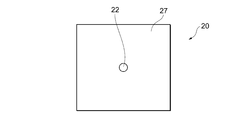
- FIG. 3A is a top view of a bonding heater used in the flip chip bonding apparatus according to the embodiment of the present invention.
- FIG. 3B is a cross-sectional view of a bonding heater used in the flip chip bonding apparatus according to the embodiment of the present invention.
- FIG. 3C is a bottom view of the bonding heater used in the flip chip bonding apparatus according to the embodiment of the present invention.
- a vacuum suction hole 22 communicating with the vacuum suction hole 16 of the attachment 10 is provided at the center of the bonding heater 20.
- the upper surface 27 of the bonding heater 20 is in contact with the lower surface 33 of the main body 31.
- the main body 31 is a member configured to include, for example, stainless steel including iron, chrome, and the like.
- the thermal conductivity of the main body 31 including stainless steel is, for example, several tens of W / m ⁇ K or less, which is smaller than the thermal conductivity of the bonding heater 20. That is, the main body 31 and the bonding heater 20 are configured to include materials having different thermal conductivities.
- the vacuum suction path 32 provided in the main body 31 is connected to the vacuum pump 44 via the second opening 35 by a pipe 41 in which an electromagnetic valve 43 is disposed in the middle.
- the vacuum suction path 32 to which the pipe 41 is connected and the vacuum suction hole 22 of the bonding heater 20 are in a vacuum state, and the attachment 10 is vacuum-adsorbed to the lower surface 26 of the bonding heater 20.
- the electromagnetic valve 43 is open, the vacuum suction path 32 of the main body 31 to which the pipe 41 is connected, the vacuum suction hole 22 of the bonding heater 20 communicating with the vacuum suction path 32, and the vacuum suction
- the vacuum suction hole 16 of the attachment 10 communicating with the hole 22 is in a vacuum state. Therefore, the surface on the protruding electrode 72 side of the semiconductor die 70 is vacuum-sucked to the surface 14 of the island 13 of the attachment 10.
- FIG. 4 is a configuration diagram showing the configuration of another flip chip bonding apparatus according to the embodiment of the present invention.
- the drip prevention unit 90 of the mounting head 60 is disposed downstream of the first bent portion 37 of the vacuum suction path 32 (suction path) in the gas suction direction, and the droplets condensed with gas or A storage unit 90A is provided for storing the solid solidified by the droplets.
- the vacuum suction path 32 further includes a second bent portion 38 provided on the downstream side of the first bent portion 37 in the gas suction direction, and the drip preventing portion 90 is connected to the first bent portion 37 and the second bent portion 38. It is provided across.
- the storage portion 90A may be configured to be disposed in the second bent portion 38.
- the main body 31 may be configured to be vertically splittable on a split surface DF passing through the storage portion 90A.
- the upper part of the main body 31 divided by the dividing surface DF is an upper main body 31A
- the lower part is a lower main body 31B.
- FIG. 5 is a cross-sectional view of the main body 31 viewed from the direction VV in FIG.
- the storage portion 90 ⁇ / b> A is disposed at a position different from the position of the vacuum suction holes 16, 22 in a cross-sectional view of the main body portion 31 orthogonal to the axial direction of the vacuum suction holes 16, 22.
- 90 A of storage parts are comprised by the solid shape.
- the vacuum suction path 32 provided in the main body 31 is configured to communicate with the vacuum suction hole 22 provided in the bonding heater 20 and communicating with the vacuum suction hole 16 of the attachment 10.
- FIG. 6 is a configuration diagram showing the configuration of another flip chip bonding apparatus according to the embodiment of the present invention.
- the drip prevention part 90 is a first bent part 37 that is directly above a vacuum suction hole 22 (through hole) as a through hole that penetrates the bonding heater 20 in the vacuum suction path 32 (suction path).
- a path heater 90B that heats the gas to a temperature equal to or higher than the condensation temperature of the gas. Since the path heater 90B heats the gas to a temperature equal to or higher than the gas condensing temperature in the first bent portion 37, the gas can be prevented from being liquefied in the vicinity of the first bent portion 37.
- the drip prevention unit 90 is disposed downstream of the first bent portion 37 of the vacuum suction path 32 (suction path) in the gas suction direction, and cools the gas to a temperature equal to or lower than the gas condensation temperature. 90C is provided.
- the vacuum suction path 32 further includes a third bent portion 39 provided downstream of the second bent portion 38 in the gas suction direction, and the drip preventing portion 90 includes the first bent portion 37, the second bent portion 38, and the second bent portion 38. It is provided over the third bent portion 39.
- the cooling unit 90 ⁇ / b> C may be configured to be disposed at the third bent portion 39.
- the main body 31 includes a path heater 90 ⁇ / b> B, a reservoir 90 ⁇ / b> A, and a cooling unit 90 ⁇ / b> C in order along the gas suction direction.
- the drip prevention unit 90 includes a condensing unit that is disposed downstream of the first bent portion 37 of the vacuum suction path 32 in the gas suction direction instead of the cooling unit 90C and increases the fluid resistance of the gas. Good. Further, the drip prevention unit 90 may further include the condensing unit in addition to the cooling unit 90C. The cooling unit 90C and the condensing unit can promote gas condensation, and the liquefied one is stored in the storing unit 90A.
- the flip chip bonding apparatus 100 forms one surface of the die body 71 on the first-stage semiconductor die 80 in which the protruding electrode 82 is formed on the upper surface of the die body 81.
- a protruding electrode 72 is formed on the other surface
- a protruding electrode 73 is formed on the other surface
- a bump 74 is formed on the tip of the protruding electrode 73 with solder or the like
- an NCF 75 is attached to the other surface where the protruding electrode 73 is provided.
- the process of mounting the eye semiconductor die 70 will be described.
- the protruding electrodes 72 and 73 may be made of, for example, copper.
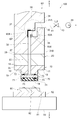
- FIG. 8 shows that the second-stage semiconductor die 70 is attracted to the attachment 10 in the process of stack-mounting the semiconductor die 70 having electrodes arranged on both sides using the flip chip bonding apparatus 100 according to the embodiment of the present invention.
- FIG. 8 shows a state.
- the first-stage semiconductor die 80 is disposed on the upper surface of the bonding stage 50.
- the vacuum pump 44 shown in FIG. 1 is driven, and the vacuum suction path 32 to which the pipe 41 is connected and the vacuum suction hole 22 of the bonding heater 20 are brought into a vacuum state, and the attachment 10 is attached to the lower surface 26 of the bonding heater 20.
- the upper surface 18 is vacuum-adsorbed.
- the mounting head 60 is moved onto the semiconductor die 70 placed on the reversal and delivery device (not shown) of the semiconductor die 70 so that the protruding electrode 72 is on the upper side.
- the electromagnetic valve 43 is opened, the vacuum suction path 32 of the main body 31 to which the pipe 41 is connected, the vacuum suction hole 22 of the bonding heater 20 communicating with the vacuum suction path 32, and the vacuum suction hole 22.
- the vacuum suction hole 16 of the attachment 10 that communicates with the vacuum is brought into a vacuum state. Therefore, the surface on the protruding electrode 72 side of the semiconductor die 70 is vacuum-sucked to the surface 14 of the island 13 of the attachment 10.
- the flip chip bonding apparatus 100 is in a state as shown in FIG. become.
- the temperature of the attachment 10 is about 100 ° C., for example, and the bump 74 is not in a molten state.
- NCF75 is also not in a low viscosity state.
- a gap corresponding to the height of the protruding electrode 72 is left between the surface 14 of the attachment 10 and the die body 71 of the semiconductor die 70. Therefore, even when the semiconductor die 70 is vacuum-adsorbed on the surface 14 of the attachment 10, the air around the semiconductor die 70 enters the inside of the vacuum suction hole 16 from the gap as shown by the arrow A1 in FIG. Try to get in.
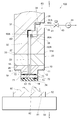
- FIG. 9 shows a state in which the attachment 10 is lowered to press the electrode of the semiconductor die 70 against the electrode of the semiconductor die 80 and the semiconductor die 70 is heated by the bonding heater 20 after the step shown in FIG. It is explanatory drawing.
- the mounting head 60 is lowered by a driving device (not shown) as indicated by a white arrow A ⁇ b> 2, and the bumps 74 of the semiconductor die 70 adsorbed on the surface 14 of the attachment 10 are vacuumed on the bonding stage 50.
- the bonding die 20 heats the semiconductor die 70 to about 250 ° C. to melt the bumps 74.
- the NCF 75 attached to the side of the semiconductor die 70 on which the protruding electrode 73 is disposed has a low viscosity, and fills the gap between the die body 81 of the semiconductor die 80 and the die body 71 of the semiconductor die 70.
- the protruding electrode 82 of the semiconductor die 80 and the protruding electrode 73 of the semiconductor die 70 are metal-bonded by the melted bumps 74, and the gap between the die body 81 of the semiconductor die 80 and the die body 71 of the semiconductor die 70.
- the resin filled with is thermoset to become a thermoset resin 75a.
- the gasification component of NCF 75 becomes gas G and stays around the semiconductor die 70. This staying gas may flow into the vacuum suction hole 16 of the attachment 10, the vacuum suction hole 22 of the bonding heater 20, and the vacuum suction path 32 of the main body 31 as indicated by an arrow A1.
- the gas G that has flowed in is heated by, for example, a path heater 90B provided in the vacuum suction path 32, and rises in the vacuum suction path 32 (for example, a range surrounded by a dotted line C in the vacuum suction path 32).
- the inside of the vacuum suction path 32 is raised as it is without being liquefied.
- the gas G that has risen is liquefied (condensed) by being cooled by the cooling unit 90 ⁇ / b> C provided in the vacuum suction path 32. Then, the droplets L are dropped from the cooling unit 90C and stored as the storage 91 in the storage unit 90A provided in the vacuum suction path 32, or the solid solidified liquid is stored as the storage 91 in the storage unit 90A. Stored.
- FIG. 10 is an explanatory view showing a state in which the attachment is raised after the process shown in FIG.
- the electromagnetic valve 43 is closed and the suction of the vacuum suction path 32 is stopped, when the mounting head 60 is raised by the drive device (not shown) as shown by the white arrow A3,
- the semiconductor die 80 and the semiconductor die 70 bonded to the semiconductor die 80 remain.
- the temperature is lowered, the melted bump 74 is solidified to become the bonding metal 74b, and the thermosetting resin 75a is cured and the upper surface of the die body 81 of the semiconductor die 80 and the lower surface of the die body 71 of the semiconductor die 70.
- the filling resin 75c fills the gap.
- the gas is heated by the path heater 90 ⁇ / b> B provided in the vacuum suction path 32 and is liquefied in the middle of rising (for example, a range surrounded by a dotted line C in the vacuum suction path 32). Without going up, the inside of the vacuum suction path 32 is raised as it is.
- the rising gas is liquefied (condensed) by being cooled by the cooling unit 90C provided in the vacuum suction path 32.
- the condensed liquid is stored in the storage part 90A provided in the vacuum suction path 32 as the stored substance 91, or the solid solidified by the liquid is stored in the storing part 90A as the stored substance 91.
- FIG. 11 is a configuration diagram showing another example of the configuration of the main body used in the flip chip bonding apparatus according to the embodiment of the present invention.
- the main body 31 is configured to be split up and down on a split surface DF passing through the storage portion 90A.
- the bottom 95 of the reservoir 90 ⁇ / b> A is provided on the lower main body 31 ⁇ / b> B divided by the dividing surface DF.
- the main body 31 includes a third opening 36 in the storage portion 90A in the upper main body 31A divided by the dividing surface DF, and the third opening 36 gradually decreases toward the downstream side in the gas suction direction.
- the diameter of one end surface S1 of the third opening 36 is larger than the diameter of the other end surface S2 downstream of the third opening 36 in the suction direction.
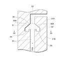
- FIG. 12 is a cross-sectional view of the main body viewed from the XII-XII direction of FIG.
- the storage portion 90 ⁇ / b> A is disposed along the outer periphery of the vacuum suction path 32.
- the liquid condensed with gas travels along the wall surface of the reservoir 90A toward the bottom 95, so that the cross section of the main body 31 perpendicular to the axial direction of the vacuum suction holes 16 and 22 shown in FIG.
- foreign matter can be appropriately stored at a position different from the positions of the vacuum suction holes 16 and 22.
- FIG. 13 is a configuration diagram showing another example of the configuration of the main body used in the flip chip bonding apparatus according to the embodiment of the present invention.
- the main body 31 may be configured to include a protrusion 90 ⁇ / b> D at a position facing the position where the storage portion 90 ⁇ / b> A is provided in the vacuum suction path 32.
- the length of the vicinity where the storage portion 90A is provided in the vacuum suction path 32 becomes longer, so that the gas can be naturally cooled. Accordingly, since it is not necessary to provide the cooling unit 90C as shown in FIGS. 7 to 10, the main body 31 can be easily manufactured and the manufacturing cost of the main body 31 can be reduced.
- the vacuum suction path 32 provided in the main body 31 includes the drip prevention unit 90. Therefore, even if the gas flowing into the vacuum suction path 32 is condensed, it is possible to prevent the liquid and the solid solidified from the liquid from dropping on the bonding heater 20. Therefore, it is possible to prevent the resin containing the gas component from sealing the vacuum suction hole 22, so that the mounting head 60 can be prevented from being damaged.
- the vacuum suction holes 16 and 22 and the vacuum suction path 32 have been described as having an oval shape.
- the shape of the vacuum suction hole is not limited to this, and may be a rectangular hole or an elliptical hole, for example. Good.
- NCF 75 is used for joining the semiconductor die 70 and the semiconductor die 80
- the present invention is not limited to this, and other types of resins can be used.
- SYMBOLS 10 Attachment, 11 ... Base, 12, 26, 33 ... Lower surface, 13 ... Island, 14 ... Surface, 16, 22 ... Vacuum suction hole, 18, 27 ... Upper surface, 19 ... First opening, 20 ... Bonding heater, DESCRIPTION OF SYMBOLS 31 ... Main-body part, 32 ... Vacuum suction path, 35 ... 2nd opening part, 36 ... 3rd opening part, 37 ... 1st bending part, 38 ... 2nd bending part, 39 ... 3rd bending part, 41 ... Piping, 43 ... Solenoid valve, 44 ... Vacuum pump, 50 ... Bonding stage, 60 ... Mounting head, 70, 80 ...
Landscapes
- Engineering & Computer Science (AREA)
- Mechanical Engineering (AREA)
- Manufacturing & Machinery (AREA)
- Microelectronics & Electronic Packaging (AREA)
- Wire Bonding (AREA)
- Supply And Installment Of Electrical Components (AREA)
Abstract
Description
上記のように本発明を実施の形態によって記載したが、この開示の一部をなす記述及び図面はこの発明を限定するものであると理解するべきではない。この開示から当業者には様々な代替実施の形態、実施例及び運用技術が明らかになるはずである。
Claims (13)
- 半導体ダイの電極と基板又は別の半導体ダイの電極とを接合する電子部品実装装置に用いる実装ヘッドであって、
半導体ダイを吸着する吸着面を有するアタッチメントと、
前記アタッチメントの前記吸着面とは反対側の面に配置され、前記アタッチメント及び前記半導体ダイを加熱するボンディングヒータと、
端面で前記ボンディングヒータを保持する本体部と、
前記アタッチメントの前記吸着面に形成された第1開口部と、
前記本体部の前記端面とは異なる面に形成された第2開口部と、
前記本体部内で前記第1開口部から吸引された気体の流路を屈曲させる第1屈曲部を有し、前記アタッチメント、前記ボンディングヒータ、及び前記本体部の内部を貫通する吸引経路であって、前記第1開口部から吸引された気体を前記第2開口部において外部に排出する吸引経路と、
前記吸引経路に形成され、前記気体が凝縮した液滴が前記ボンディングヒータに滴下するのを抑制する滴下防止部と、
を備える、
実装ヘッド。 - 前記滴下防止部は、前記吸引経路の前記第1屈曲部よりも前記気体の吸引方向下流側において配置され、前記気体が凝縮した前記液滴又は前記液滴が凝固した固体を貯留する貯留部を備える、
請求項1に記載の実装ヘッド。 - 前記滴下防止部は、前記吸引経路において前記ボンディングヒータを貫通する貫通孔の直上部に配置され、前記気体の凝縮温度以上の温度に前記気体を加熱する経路ヒータを備える、
請求項1に記載の実装ヘッド。 - 前記滴下防止部は、前記吸引経路の前記第1屈曲部よりも前記気体の吸引方向下流側において配置され、前記気体の凝縮温度以下の温度に前記気体を冷却する冷却部を備える、
請求項1に記載の実装ヘッド。 - 前記滴下防止部は、前記吸引経路の前記第1屈曲部よりも前記気体の吸引方向下流側において配置され、前記気体の流体抵抗を増加させる凝縮部を備える、
請求項1に記載の実装ヘッド。 - 前記吸引経路は、前記第1屈曲部よりも前記気体の吸引方向下流側に設けられた第2屈曲部を更に備え、
前記滴下防止部は、前記第1屈曲部及び前記第2屈曲部に渡って設けられる、
請求項1に記載の実装ヘッド。 - 前記気体が凝縮した前記液滴又は前記液滴が凝固した固体を貯留する貯留部は、前記第2屈曲部に配置されている、
請求項6に記載の実装ヘッド。 - 前記本体部は、前記気体が凝縮した前記液滴又は前記液滴が凝固した固体を貯留する貯留部を通る分割面において上下に分割可能に構成されている、
請求項1から7のいずれか一項に記載の実装ヘッド。 - 前記貯留部の底部が前記分割面で分割した下部本体部に設けられている、
請求項8に記載の実装ヘッド。 - 前記本体部は、前記分割面で分割した上部本体部に第3開口部を備え、
前記第3開口部は、前記気体の吸引方向下流側に向かって次第に小さくなるようにテーパ状に形成されており、前記第3開口部の一端面の直径が前記第3開口部の前記吸引方向下流側の他の端面の直径よりも大きい、
請求項8に記載の実装ヘッド。 - 前記本体部は、前記吸引経路において前記ボンディングヒータを貫通する貫通孔の直上部に配置され、前記気体の凝縮温度以上の温度に前記気体を加熱する経路ヒータと、前記吸引経路の前記第1屈曲部よりも前記気体の吸引方向下流側において配置され、前記気体が凝縮した前記液滴又は前記液滴が凝固した固体を貯留する貯留部と、前記吸引経路の前記第1屈曲部よりも前記気体の吸引方向下流側において配置され、前記気体の凝縮温度以下の温度に前記気体を冷却する冷却部と、を前記気体の吸引方向に沿って順次備えている、
請求項1に記載の実装ヘッド。 - 前記本体部は、前記吸引経路において、前記気体が凝縮した前記液滴又は前記液滴が凝固した固体を貯留する貯留部が設けられている位置に対向する位置に突起部を更に備える、請求項1に記載の実装ヘッド。
- 前記ボンディングヒータと前記本体部とは、異なる熱伝導率を有する材料を含んで構成される、請求項1に記載の実装ヘッド。
Priority Applications (5)
| Application Number | Priority Date | Filing Date | Title |
|---|---|---|---|
| US16/464,276 US11302666B2 (en) | 2016-11-17 | 2017-11-17 | Mounting head |
| JP2018551707A JP6753948B2 (ja) | 2016-11-17 | 2017-11-17 | 実装ヘッド |
| CN201780083286.6A CN110178457B (zh) | 2016-11-17 | 2017-11-17 | 安装头 |
| SG11201910002S SG11201910002SA (en) | 2016-11-17 | 2017-11-17 | Mounting head |
| KR1020197017132A KR102228795B1 (ko) | 2016-11-17 | 2017-11-17 | 실장 헤드 |
Applications Claiming Priority (2)
| Application Number | Priority Date | Filing Date | Title |
|---|---|---|---|
| JP2016-224261 | 2016-11-17 | ||
| JP2016224261 | 2016-11-17 |
Publications (1)
| Publication Number | Publication Date |
|---|---|
| WO2018092883A1 true WO2018092883A1 (ja) | 2018-05-24 |
Family
ID=62146568
Family Applications (1)
| Application Number | Title | Priority Date | Filing Date |
|---|---|---|---|
| PCT/JP2017/041484 Ceased WO2018092883A1 (ja) | 2016-11-17 | 2017-11-17 | 実装ヘッド |
Country Status (7)
| Country | Link |
|---|---|
| US (1) | US11302666B2 (ja) |
| JP (1) | JP6753948B2 (ja) |
| KR (1) | KR102228795B1 (ja) |
| CN (1) | CN110178457B (ja) |
| SG (1) | SG11201910002SA (ja) |
| TW (1) | TWI661499B (ja) |
| WO (1) | WO2018092883A1 (ja) |
Families Citing this family (4)
| Publication number | Priority date | Publication date | Assignee | Title |
|---|---|---|---|---|
| TW202119533A (zh) * | 2019-11-04 | 2021-05-16 | 台灣愛司帝科技股份有限公司 | 具有晶片吸附功能的晶片承載結構 |
| US11961817B2 (en) * | 2021-02-26 | 2024-04-16 | Taiwan Semiconductor Manufacturing Company, Ltd. | Apparatus and method for forming a package structure |
| JP7695522B2 (ja) * | 2021-05-11 | 2025-06-19 | 澁谷工業株式会社 | ボンディング装置 |
| KR20250145245A (ko) * | 2024-03-28 | 2025-10-13 | 한화세미텍 주식회사 | 다이 본딩 장치 |
Citations (2)
| Publication number | Priority date | Publication date | Assignee | Title |
|---|---|---|---|---|
| JP2011086699A (ja) * | 2009-10-14 | 2011-04-28 | Canon Machinery Inc | ボンディング装置 |
| WO2012165313A1 (ja) * | 2011-05-27 | 2012-12-06 | 東レエンジニアリング株式会社 | 実装方法および実装装置 |
Family Cites Families (14)
| Publication number | Priority date | Publication date | Assignee | Title |
|---|---|---|---|---|
| US4659004A (en) * | 1984-02-24 | 1987-04-21 | Pace, Incorporated | Device for attaching modular electronic components to or removing them from an insulative device |
| US5419481A (en) * | 1993-09-21 | 1995-05-30 | Air-Vac Engineering Company, Inc. | Process and apparatus for attaching/deataching land grid array components |
| US5553768A (en) * | 1993-09-21 | 1996-09-10 | Air-Vac Engineering Company, Inc. | Heat-control process and apparatus for attachment/detachment of soldered components |
| US5785237A (en) * | 1996-08-30 | 1998-07-28 | Air-Vac Engineering Company, Inc. | Differential multi-flow control nozzles, apparatus and process |
| US6016949A (en) * | 1997-07-01 | 2000-01-25 | International Business Machines Corporation | Integrated placement and soldering pickup head and method of using |
| US6537400B1 (en) * | 2000-03-06 | 2003-03-25 | Micron Technology, Inc. | Automated method of attaching flip chip devices to a substrate |
| JP3721559B2 (ja) * | 2002-03-28 | 2005-11-30 | 東レエンジニアリング株式会社 | チップ実装方法 |
| JP5008952B2 (ja) * | 2006-11-15 | 2012-08-22 | キヤノンマシナリー株式会社 | ダイボンダおよびダイボンディング方法 |
| US7555832B2 (en) * | 2007-03-19 | 2009-07-07 | Infineon Technologies Ag | Semiconductor chip attachment |
| JP2010212274A (ja) | 2009-03-06 | 2010-09-24 | Nec Corp | チップ実装機、及び、チップの実装方法 |
| JP2012165313A (ja) | 2011-02-09 | 2012-08-30 | Sony Corp | 編集装置及び方法、並びにプログラム |
| JP6064388B2 (ja) * | 2012-06-28 | 2017-01-25 | 澁谷工業株式会社 | ボンディングヘッド |
| JP5683660B1 (ja) * | 2013-09-19 | 2015-03-11 | 株式会社カイジョー | ダイボンディング装置 |
| KR101685545B1 (ko) * | 2015-04-29 | 2016-12-12 | 주식회사 바른전자 | 인쇄회로기판을 이용한 멀티 다이 스태킹 방법 및 이를 이용한 반도체 패키지 |
-
2017
- 2017-11-17 JP JP2018551707A patent/JP6753948B2/ja active Active
- 2017-11-17 WO PCT/JP2017/041484 patent/WO2018092883A1/ja not_active Ceased
- 2017-11-17 TW TW106139877A patent/TWI661499B/zh active
- 2017-11-17 CN CN201780083286.6A patent/CN110178457B/zh active Active
- 2017-11-17 SG SG11201910002S patent/SG11201910002SA/en unknown
- 2017-11-17 KR KR1020197017132A patent/KR102228795B1/ko active Active
- 2017-11-17 US US16/464,276 patent/US11302666B2/en active Active
Patent Citations (2)
| Publication number | Priority date | Publication date | Assignee | Title |
|---|---|---|---|---|
| JP2011086699A (ja) * | 2009-10-14 | 2011-04-28 | Canon Machinery Inc | ボンディング装置 |
| WO2012165313A1 (ja) * | 2011-05-27 | 2012-12-06 | 東レエンジニアリング株式会社 | 実装方法および実装装置 |
Also Published As
| Publication number | Publication date |
|---|---|
| SG11201910002SA (en) | 2019-11-28 |
| KR102228795B1 (ko) | 2021-03-17 |
| CN110178457A (zh) | 2019-08-27 |
| US20200051947A1 (en) | 2020-02-13 |
| CN110178457B (zh) | 2020-10-30 |
| JPWO2018092883A1 (ja) | 2019-06-24 |
| JP6753948B2 (ja) | 2020-09-09 |
| KR20190086504A (ko) | 2019-07-22 |
| TW201820509A (zh) | 2018-06-01 |
| TWI661499B (zh) | 2019-06-01 |
| US11302666B2 (en) | 2022-04-12 |
Similar Documents
| Publication | Publication Date | Title |
|---|---|---|
| JP6603401B2 (ja) | ボンディング装置 | |
| KR102220667B1 (ko) | 전자부품 실장 장치 | |
| JP6753948B2 (ja) | 実装ヘッド | |
| US8048479B2 (en) | Method for placing material onto a target board by means of a transfer board | |
| US8381966B2 (en) | Flip chip assembly method employing post-contact differential heating | |
| TWI683719B (zh) | 助焊劑轉印裝置 | |
| US9059241B2 (en) | 3D assembly for interposer bow | |
| CA2852661A1 (en) | System for fast and accurate filling of a two-phase cooling device, notably a heat pipe, adapted for use in an automated process | |
| US7032653B1 (en) | Tower-type heat pipe and method for making the same | |
| JP2010212274A (ja) | チップ実装機、及び、チップの実装方法 | |
| TWI618157B (zh) | Electronic component mounting device | |
| JP2015053418A (ja) | 半導体製造装置 | |
| Zheng et al. | Effect of die shape on die tilt in die attach process | |
| JP5938132B1 (ja) | 部品接合装置及び部品接合システム | |
| KR101036134B1 (ko) | 솔더 범프 전달 장치 | |
| JP2008072015A (ja) | 電子部品実装装置 | |
| CN103824824B (zh) | 一种集成散热结构及其制造方法 | |
| KR20090075991A (ko) | 솔더 범퍼 형성용 템플레이트 및 솔더 범퍼 형성 방법 | |
| JP2004342685A (ja) | ベアチップのマウント方法 | |
| KR20060135372A (ko) | 흡판으로 공기제거와 충전을 행하는 열파이프 제조방법 | |
| KR20110026151A (ko) | 솔더 범프 형성 장치 | |
| JP2010267802A (ja) | 半導体装置の製造装置および製造方法、ならびに半導体装置 |
Legal Events
| Date | Code | Title | Description |
|---|---|---|---|
| 121 | Ep: the epo has been informed by wipo that ep was designated in this application |
Ref document number: 17871962 Country of ref document: EP Kind code of ref document: A1 |
|
| ENP | Entry into the national phase |
Ref document number: 2018551707 Country of ref document: JP Kind code of ref document: A |
|
| NENP | Non-entry into the national phase |
Ref country code: DE |
|
| ENP | Entry into the national phase |
Ref document number: 20197017132 Country of ref document: KR Kind code of ref document: A |
|
| 122 | Ep: pct application non-entry in european phase |
Ref document number: 17871962 Country of ref document: EP Kind code of ref document: A1 |