WO2018092407A1 - Dispositif électronique et procédé permettant de produire ce dernier - Google Patents
Dispositif électronique et procédé permettant de produire ce dernier Download PDFInfo
- Publication number
- WO2018092407A1 WO2018092407A1 PCT/JP2017/033675 JP2017033675W WO2018092407A1 WO 2018092407 A1 WO2018092407 A1 WO 2018092407A1 JP 2017033675 W JP2017033675 W JP 2017033675W WO 2018092407 A1 WO2018092407 A1 WO 2018092407A1
- Authority
- WO
- WIPO (PCT)
- Prior art keywords
- molded body
- resin molded
- wiring
- electronic device
- sheet
- Prior art date
Links
- 238000004519 manufacturing process Methods 0.000 title claims description 30
- 229920005989 resin Polymers 0.000 claims abstract description 179
- 239000011347 resin Substances 0.000 claims abstract description 179
- 238000000034 method Methods 0.000 claims description 47
- 238000000465 moulding Methods 0.000 claims description 31
- 239000000463 material Substances 0.000 claims description 26
- 230000008569 process Effects 0.000 claims description 15
- 238000005452 bending Methods 0.000 claims description 13
- 239000000945 filler Substances 0.000 claims description 6
- 238000009751 slip forming Methods 0.000 claims description 3
- 239000000758 substrate Substances 0.000 description 37
- 238000001746 injection moulding Methods 0.000 description 12
- 239000000853 adhesive Substances 0.000 description 9
- 230000001070 adhesive effect Effects 0.000 description 8
- 238000012937 correction Methods 0.000 description 7
- 238000010586 diagram Methods 0.000 description 5
- 238000007641 inkjet printing Methods 0.000 description 5
- 229920000139 polyethylene terephthalate Polymers 0.000 description 5
- 239000005020 polyethylene terephthalate Substances 0.000 description 5
- 239000004743 Polypropylene Substances 0.000 description 4
- 239000012790 adhesive layer Substances 0.000 description 4
- 229920001971 elastomer Polymers 0.000 description 4
- 230000004048 modification Effects 0.000 description 4
- 238000012986 modification Methods 0.000 description 4
- 239000004417 polycarbonate Substances 0.000 description 4
- 229920000515 polycarbonate Polymers 0.000 description 4
- -1 polypropylene Polymers 0.000 description 4
- 229920001155 polypropylene Polymers 0.000 description 4
- BQCADISMDOOEFD-UHFFFAOYSA-N Silver Chemical compound [Ag] BQCADISMDOOEFD-UHFFFAOYSA-N 0.000 description 3
- 239000004676 acrylonitrile butadiene styrene Substances 0.000 description 3
- 239000000806 elastomer Substances 0.000 description 3
- 229910052709 silver Inorganic materials 0.000 description 3
- 239000004332 silver Substances 0.000 description 3
- 238000012360 testing method Methods 0.000 description 3
- RYGMFSIKBFXOCR-UHFFFAOYSA-N Copper Chemical compound [Cu] RYGMFSIKBFXOCR-UHFFFAOYSA-N 0.000 description 2
- 239000004952 Polyamide Substances 0.000 description 2
- 239000004642 Polyimide Substances 0.000 description 2
- 239000004734 Polyphenylene sulfide Substances 0.000 description 2
- 230000008901 benefit Effects 0.000 description 2
- 239000003990 capacitor Substances 0.000 description 2
- 229910052802 copper Inorganic materials 0.000 description 2
- 239000010949 copper Substances 0.000 description 2
- 238000013461 design Methods 0.000 description 2
- 239000011521 glass Substances 0.000 description 2
- 238000002347 injection Methods 0.000 description 2
- 239000007924 injection Substances 0.000 description 2
- 238000009434 installation Methods 0.000 description 2
- 239000010410 layer Substances 0.000 description 2
- 229920002647 polyamide Polymers 0.000 description 2
- 229920001721 polyimide Polymers 0.000 description 2
- 229920000069 polyphenylene sulfide Polymers 0.000 description 2
- 229910000679 solder Inorganic materials 0.000 description 2
- 229920002799 BoPET Polymers 0.000 description 1
- OKTJSMMVPCPJKN-UHFFFAOYSA-N Carbon Chemical compound [C] OKTJSMMVPCPJKN-UHFFFAOYSA-N 0.000 description 1
- 239000000443 aerosol Substances 0.000 description 1
- XAGFODPZIPBFFR-UHFFFAOYSA-N aluminium Chemical compound [Al] XAGFODPZIPBFFR-UHFFFAOYSA-N 0.000 description 1
- 229910052782 aluminium Inorganic materials 0.000 description 1
- 230000015572 biosynthetic process Effects 0.000 description 1
- 230000036772 blood pressure Effects 0.000 description 1
- 229910052799 carbon Inorganic materials 0.000 description 1
- 230000008859 change Effects 0.000 description 1
- 239000004020 conductor Substances 0.000 description 1
- 238000005516 engineering process Methods 0.000 description 1
- 239000011229 interlayer Substances 0.000 description 1
- 230000001678 irradiating effect Effects 0.000 description 1
- 230000007794 irritation Effects 0.000 description 1
- 238000010030 laminating Methods 0.000 description 1
- 239000011112 polyethylene naphthalate Substances 0.000 description 1
- 239000004814 polyurethane Substances 0.000 description 1
- 238000007639 printing Methods 0.000 description 1
- 238000005476 soldering Methods 0.000 description 1
- 238000005507 spraying Methods 0.000 description 1
- 238000009864 tensile test Methods 0.000 description 1
Images


Classifications
-
- H—ELECTRICITY
- H01—ELECTRIC ELEMENTS
- H01L—SEMICONDUCTOR DEVICES NOT COVERED BY CLASS H10
- H01L21/00—Processes or apparatus adapted for the manufacture or treatment of semiconductor or solid state devices or of parts thereof
- H01L21/02—Manufacture or treatment of semiconductor devices or of parts thereof
- H01L21/04—Manufacture or treatment of semiconductor devices or of parts thereof the devices having potential barriers, e.g. a PN junction, depletion layer or carrier concentration layer
- H01L21/50—Assembly of semiconductor devices using processes or apparatus not provided for in a single one of the subgroups H01L21/06 - H01L21/326, e.g. sealing of a cap to a base of a container
- H01L21/56—Encapsulations, e.g. encapsulation layers, coatings
- H01L21/565—Moulds
-
- H—ELECTRICITY
- H01—ELECTRIC ELEMENTS
- H01L—SEMICONDUCTOR DEVICES NOT COVERED BY CLASS H10
- H01L21/00—Processes or apparatus adapted for the manufacture or treatment of semiconductor or solid state devices or of parts thereof
- H01L21/02—Manufacture or treatment of semiconductor devices or of parts thereof
- H01L21/04—Manufacture or treatment of semiconductor devices or of parts thereof the devices having potential barriers, e.g. a PN junction, depletion layer or carrier concentration layer
- H01L21/50—Assembly of semiconductor devices using processes or apparatus not provided for in a single one of the subgroups H01L21/06 - H01L21/326, e.g. sealing of a cap to a base of a container
- H01L21/56—Encapsulations, e.g. encapsulation layers, coatings
- H01L21/565—Moulds
- H01L21/566—Release layers for moulds, e.g. release layers, layers against residue during moulding
-
- H—ELECTRICITY
- H01—ELECTRIC ELEMENTS
- H01L—SEMICONDUCTOR DEVICES NOT COVERED BY CLASS H10
- H01L21/00—Processes or apparatus adapted for the manufacture or treatment of semiconductor or solid state devices or of parts thereof
- H01L21/02—Manufacture or treatment of semiconductor devices or of parts thereof
- H01L21/04—Manufacture or treatment of semiconductor devices or of parts thereof the devices having potential barriers, e.g. a PN junction, depletion layer or carrier concentration layer
- H01L21/50—Assembly of semiconductor devices using processes or apparatus not provided for in a single one of the subgroups H01L21/06 - H01L21/326, e.g. sealing of a cap to a base of a container
- H01L21/56—Encapsulations, e.g. encapsulation layers, coatings
- H01L21/568—Temporary substrate used as encapsulation process aid
-
- H—ELECTRICITY
- H01—ELECTRIC ELEMENTS
- H01L—SEMICONDUCTOR DEVICES NOT COVERED BY CLASS H10
- H01L23/00—Details of semiconductor or other solid state devices
- H01L23/28—Encapsulations, e.g. encapsulating layers, coatings, e.g. for protection
- H01L23/31—Encapsulations, e.g. encapsulating layers, coatings, e.g. for protection characterised by the arrangement or shape
- H01L23/3107—Encapsulations, e.g. encapsulating layers, coatings, e.g. for protection characterised by the arrangement or shape the device being completely enclosed
- H01L23/3135—Double encapsulation or coating and encapsulation
-
- H—ELECTRICITY
- H01—ELECTRIC ELEMENTS
- H01L—SEMICONDUCTOR DEVICES NOT COVERED BY CLASS H10
- H01L23/00—Details of semiconductor or other solid state devices
- H01L23/52—Arrangements for conducting electric current within the device in operation from one component to another, i.e. interconnections, e.g. wires, lead frames
- H01L23/538—Arrangements for conducting electric current within the device in operation from one component to another, i.e. interconnections, e.g. wires, lead frames the interconnection structure between a plurality of semiconductor chips being formed on, or in, insulating substrates
- H01L23/5387—Flexible insulating substrates
-
- H—ELECTRICITY
- H01—ELECTRIC ELEMENTS
- H01L—SEMICONDUCTOR DEVICES NOT COVERED BY CLASS H10
- H01L24/00—Arrangements for connecting or disconnecting semiconductor or solid-state bodies; Methods or apparatus related thereto
- H01L24/01—Means for bonding being attached to, or being formed on, the surface to be connected, e.g. chip-to-package, die-attach, "first-level" interconnects; Manufacturing methods related thereto
- H01L24/02—Bonding areas ; Manufacturing methods related thereto
- H01L24/03—Manufacturing methods
-
- H—ELECTRICITY
- H01—ELECTRIC ELEMENTS
- H01L—SEMICONDUCTOR DEVICES NOT COVERED BY CLASS H10
- H01L24/00—Arrangements for connecting or disconnecting semiconductor or solid-state bodies; Methods or apparatus related thereto
- H01L24/01—Means for bonding being attached to, or being formed on, the surface to be connected, e.g. chip-to-package, die-attach, "first-level" interconnects; Manufacturing methods related thereto
- H01L24/18—High density interconnect [HDI] connectors; Manufacturing methods related thereto
- H01L24/23—Structure, shape, material or disposition of the high density interconnect connectors after the connecting process
- H01L24/24—Structure, shape, material or disposition of the high density interconnect connectors after the connecting process of an individual high density interconnect connector
-
- H—ELECTRICITY
- H01—ELECTRIC ELEMENTS
- H01L—SEMICONDUCTOR DEVICES NOT COVERED BY CLASS H10
- H01L24/00—Arrangements for connecting or disconnecting semiconductor or solid-state bodies; Methods or apparatus related thereto
- H01L24/80—Methods for connecting semiconductor or other solid state bodies using means for bonding being attached to, or being formed on, the surface to be connected
- H01L24/82—Methods for connecting semiconductor or other solid state bodies using means for bonding being attached to, or being formed on, the surface to be connected by forming build-up interconnects at chip-level, e.g. for high density interconnects [HDI]
-
- H—ELECTRICITY
- H05—ELECTRIC TECHNIQUES NOT OTHERWISE PROVIDED FOR
- H05K—PRINTED CIRCUITS; CASINGS OR CONSTRUCTIONAL DETAILS OF ELECTRIC APPARATUS; MANUFACTURE OF ASSEMBLAGES OF ELECTRICAL COMPONENTS
- H05K1/00—Printed circuits
- H05K1/02—Details
- H05K1/0277—Bendability or stretchability details
- H05K1/028—Bending or folding regions of flexible printed circuits
-
- H—ELECTRICITY
- H05—ELECTRIC TECHNIQUES NOT OTHERWISE PROVIDED FOR
- H05K—PRINTED CIRCUITS; CASINGS OR CONSTRUCTIONAL DETAILS OF ELECTRIC APPARATUS; MANUFACTURE OF ASSEMBLAGES OF ELECTRICAL COMPONENTS
- H05K1/00—Printed circuits
- H05K1/02—Details
- H05K1/14—Structural association of two or more printed circuits
- H05K1/147—Structural association of two or more printed circuits at least one of the printed circuits being bent or folded, e.g. by using a flexible printed circuit
-
- H—ELECTRICITY
- H05—ELECTRIC TECHNIQUES NOT OTHERWISE PROVIDED FOR
- H05K—PRINTED CIRCUITS; CASINGS OR CONSTRUCTIONAL DETAILS OF ELECTRIC APPARATUS; MANUFACTURE OF ASSEMBLAGES OF ELECTRICAL COMPONENTS
- H05K3/00—Apparatus or processes for manufacturing printed circuits
- H05K3/22—Secondary treatment of printed circuits
- H05K3/28—Applying non-metallic protective coatings
- H05K3/284—Applying non-metallic protective coatings for encapsulating mounted components
-
- H—ELECTRICITY
- H01—ELECTRIC ELEMENTS
- H01L—SEMICONDUCTOR DEVICES NOT COVERED BY CLASS H10
- H01L2224/00—Indexing scheme for arrangements for connecting or disconnecting semiconductor or solid-state bodies and methods related thereto as covered by H01L24/00
- H01L2224/01—Means for bonding being attached to, or being formed on, the surface to be connected, e.g. chip-to-package, die-attach, "first-level" interconnects; Manufacturing methods related thereto
- H01L2224/02—Bonding areas; Manufacturing methods related thereto
- H01L2224/04—Structure, shape, material or disposition of the bonding areas prior to the connecting process
- H01L2224/04105—Bonding areas formed on an encapsulation of the semiconductor or solid-state body, e.g. bonding areas on chip-scale packages
-
- H—ELECTRICITY
- H01—ELECTRIC ELEMENTS
- H01L—SEMICONDUCTOR DEVICES NOT COVERED BY CLASS H10
- H01L2224/00—Indexing scheme for arrangements for connecting or disconnecting semiconductor or solid-state bodies and methods related thereto as covered by H01L24/00
- H01L2224/01—Means for bonding being attached to, or being formed on, the surface to be connected, e.g. chip-to-package, die-attach, "first-level" interconnects; Manufacturing methods related thereto
- H01L2224/10—Bump connectors; Manufacturing methods related thereto
- H01L2224/15—Structure, shape, material or disposition of the bump connectors after the connecting process
- H01L2224/16—Structure, shape, material or disposition of the bump connectors after the connecting process of an individual bump connector
- H01L2224/161—Disposition
- H01L2224/16151—Disposition the bump connector connecting between a semiconductor or solid-state body and an item not being a semiconductor or solid-state body, e.g. chip-to-substrate, chip-to-passive
- H01L2224/16221—Disposition the bump connector connecting between a semiconductor or solid-state body and an item not being a semiconductor or solid-state body, e.g. chip-to-substrate, chip-to-passive the body and the item being stacked
- H01L2224/16225—Disposition the bump connector connecting between a semiconductor or solid-state body and an item not being a semiconductor or solid-state body, e.g. chip-to-substrate, chip-to-passive the body and the item being stacked the item being non-metallic, e.g. insulating substrate with or without metallisation
-
- H—ELECTRICITY
- H01—ELECTRIC ELEMENTS
- H01L—SEMICONDUCTOR DEVICES NOT COVERED BY CLASS H10
- H01L2224/00—Indexing scheme for arrangements for connecting or disconnecting semiconductor or solid-state bodies and methods related thereto as covered by H01L24/00
- H01L2224/01—Means for bonding being attached to, or being formed on, the surface to be connected, e.g. chip-to-package, die-attach, "first-level" interconnects; Manufacturing methods related thereto
- H01L2224/18—High density interconnect [HDI] connectors; Manufacturing methods related thereto
- H01L2224/23—Structure, shape, material or disposition of the high density interconnect connectors after the connecting process
- H01L2224/24—Structure, shape, material or disposition of the high density interconnect connectors after the connecting process of an individual high density interconnect connector
- H01L2224/2401—Structure
- H01L2224/24011—Deposited, e.g. MCM-D type
-
- H—ELECTRICITY
- H01—ELECTRIC ELEMENTS
- H01L—SEMICONDUCTOR DEVICES NOT COVERED BY CLASS H10
- H01L2224/00—Indexing scheme for arrangements for connecting or disconnecting semiconductor or solid-state bodies and methods related thereto as covered by H01L24/00
- H01L2224/01—Means for bonding being attached to, or being formed on, the surface to be connected, e.g. chip-to-package, die-attach, "first-level" interconnects; Manufacturing methods related thereto
- H01L2224/18—High density interconnect [HDI] connectors; Manufacturing methods related thereto
- H01L2224/23—Structure, shape, material or disposition of the high density interconnect connectors after the connecting process
- H01L2224/24—Structure, shape, material or disposition of the high density interconnect connectors after the connecting process of an individual high density interconnect connector
- H01L2224/241—Disposition
- H01L2224/24101—Connecting bonding areas at the same height
-
- H—ELECTRICITY
- H01—ELECTRIC ELEMENTS
- H01L—SEMICONDUCTOR DEVICES NOT COVERED BY CLASS H10
- H01L2224/00—Indexing scheme for arrangements for connecting or disconnecting semiconductor or solid-state bodies and methods related thereto as covered by H01L24/00
- H01L2224/01—Means for bonding being attached to, or being formed on, the surface to be connected, e.g. chip-to-package, die-attach, "first-level" interconnects; Manufacturing methods related thereto
- H01L2224/18—High density interconnect [HDI] connectors; Manufacturing methods related thereto
- H01L2224/23—Structure, shape, material or disposition of the high density interconnect connectors after the connecting process
- H01L2224/24—Structure, shape, material or disposition of the high density interconnect connectors after the connecting process of an individual high density interconnect connector
- H01L2224/241—Disposition
- H01L2224/24135—Connecting between different semiconductor or solid-state bodies, i.e. chip-to-chip
- H01L2224/24137—Connecting between different semiconductor or solid-state bodies, i.e. chip-to-chip the bodies being arranged next to each other, e.g. on a common substrate
-
- H—ELECTRICITY
- H01—ELECTRIC ELEMENTS
- H01L—SEMICONDUCTOR DEVICES NOT COVERED BY CLASS H10
- H01L2224/00—Indexing scheme for arrangements for connecting or disconnecting semiconductor or solid-state bodies and methods related thereto as covered by H01L24/00
- H01L2224/01—Means for bonding being attached to, or being formed on, the surface to be connected, e.g. chip-to-package, die-attach, "first-level" interconnects; Manufacturing methods related thereto
- H01L2224/18—High density interconnect [HDI] connectors; Manufacturing methods related thereto
- H01L2224/23—Structure, shape, material or disposition of the high density interconnect connectors after the connecting process
- H01L2224/24—Structure, shape, material or disposition of the high density interconnect connectors after the connecting process of an individual high density interconnect connector
- H01L2224/241—Disposition
- H01L2224/24151—Connecting between a semiconductor or solid-state body and an item not being a semiconductor or solid-state body, e.g. chip-to-substrate, chip-to-passive
- H01L2224/24153—Connecting between a semiconductor or solid-state body and an item not being a semiconductor or solid-state body, e.g. chip-to-substrate, chip-to-passive the body and the item being arranged next to each other, e.g. on a common substrate
- H01L2224/24195—Connecting between a semiconductor or solid-state body and an item not being a semiconductor or solid-state body, e.g. chip-to-substrate, chip-to-passive the body and the item being arranged next to each other, e.g. on a common substrate the item being a discrete passive component
-
- H—ELECTRICITY
- H01—ELECTRIC ELEMENTS
- H01L—SEMICONDUCTOR DEVICES NOT COVERED BY CLASS H10
- H01L2224/00—Indexing scheme for arrangements for connecting or disconnecting semiconductor or solid-state bodies and methods related thereto as covered by H01L24/00
- H01L2224/01—Means for bonding being attached to, or being formed on, the surface to be connected, e.g. chip-to-package, die-attach, "first-level" interconnects; Manufacturing methods related thereto
- H01L2224/18—High density interconnect [HDI] connectors; Manufacturing methods related thereto
- H01L2224/23—Structure, shape, material or disposition of the high density interconnect connectors after the connecting process
- H01L2224/24—Structure, shape, material or disposition of the high density interconnect connectors after the connecting process of an individual high density interconnect connector
- H01L2224/245—Material
-
- H—ELECTRICITY
- H01—ELECTRIC ELEMENTS
- H01L—SEMICONDUCTOR DEVICES NOT COVERED BY CLASS H10
- H01L2224/00—Indexing scheme for arrangements for connecting or disconnecting semiconductor or solid-state bodies and methods related thereto as covered by H01L24/00
- H01L2224/01—Means for bonding being attached to, or being formed on, the surface to be connected, e.g. chip-to-package, die-attach, "first-level" interconnects; Manufacturing methods related thereto
- H01L2224/18—High density interconnect [HDI] connectors; Manufacturing methods related thereto
- H01L2224/23—Structure, shape, material or disposition of the high density interconnect connectors after the connecting process
- H01L2224/25—Structure, shape, material or disposition of the high density interconnect connectors after the connecting process of a plurality of high density interconnect connectors
- H01L2224/251—Disposition
- H01L2224/2512—Layout
- H01L2224/25175—Parallel arrangements
-
- H—ELECTRICITY
- H01—ELECTRIC ELEMENTS
- H01L—SEMICONDUCTOR DEVICES NOT COVERED BY CLASS H10
- H01L2224/00—Indexing scheme for arrangements for connecting or disconnecting semiconductor or solid-state bodies and methods related thereto as covered by H01L24/00
- H01L2224/80—Methods for connecting semiconductor or other solid state bodies using means for bonding being attached to, or being formed on, the surface to be connected
- H01L2224/82—Methods for connecting semiconductor or other solid state bodies using means for bonding being attached to, or being formed on, the surface to be connected by forming build-up interconnects at chip-level, e.g. for high density interconnects [HDI]
- H01L2224/821—Forming a build-up interconnect
- H01L2224/82101—Forming a build-up interconnect by additive methods, e.g. direct writing
- H01L2224/82102—Forming a build-up interconnect by additive methods, e.g. direct writing using jetting, e.g. ink jet
-
- H—ELECTRICITY
- H01—ELECTRIC ELEMENTS
- H01L—SEMICONDUCTOR DEVICES NOT COVERED BY CLASS H10
- H01L2224/00—Indexing scheme for arrangements for connecting or disconnecting semiconductor or solid-state bodies and methods related thereto as covered by H01L24/00
- H01L2224/93—Batch processes
- H01L2224/95—Batch processes at chip-level, i.e. with connecting carried out on a plurality of singulated devices, i.e. on diced chips
- H01L2224/96—Batch processes at chip-level, i.e. with connecting carried out on a plurality of singulated devices, i.e. on diced chips the devices being encapsulated in a common layer, e.g. neo-wafer or pseudo-wafer, said common layer being separable into individual assemblies after connecting
-
- H—ELECTRICITY
- H01—ELECTRIC ELEMENTS
- H01L—SEMICONDUCTOR DEVICES NOT COVERED BY CLASS H10
- H01L23/00—Details of semiconductor or other solid state devices
- H01L23/28—Encapsulations, e.g. encapsulating layers, coatings, e.g. for protection
- H01L23/31—Encapsulations, e.g. encapsulating layers, coatings, e.g. for protection characterised by the arrangement or shape
-
- H—ELECTRICITY
- H01—ELECTRIC ELEMENTS
- H01L—SEMICONDUCTOR DEVICES NOT COVERED BY CLASS H10
- H01L23/00—Details of semiconductor or other solid state devices
- H01L23/52—Arrangements for conducting electric current within the device in operation from one component to another, i.e. interconnections, e.g. wires, lead frames
- H01L23/538—Arrangements for conducting electric current within the device in operation from one component to another, i.e. interconnections, e.g. wires, lead frames the interconnection structure between a plurality of semiconductor chips being formed on, or in, insulating substrates
- H01L23/5385—Assembly of a plurality of insulating substrates
-
- H—ELECTRICITY
- H01—ELECTRIC ELEMENTS
- H01L—SEMICONDUCTOR DEVICES NOT COVERED BY CLASS H10
- H01L23/00—Details of semiconductor or other solid state devices
- H01L23/52—Arrangements for conducting electric current within the device in operation from one component to another, i.e. interconnections, e.g. wires, lead frames
- H01L23/538—Arrangements for conducting electric current within the device in operation from one component to another, i.e. interconnections, e.g. wires, lead frames the interconnection structure between a plurality of semiconductor chips being formed on, or in, insulating substrates
- H01L23/5389—Arrangements for conducting electric current within the device in operation from one component to another, i.e. interconnections, e.g. wires, lead frames the interconnection structure between a plurality of semiconductor chips being formed on, or in, insulating substrates the chips being integrally enclosed by the interconnect and support structures
-
- H—ELECTRICITY
- H01—ELECTRIC ELEMENTS
- H01L—SEMICONDUCTOR DEVICES NOT COVERED BY CLASS H10
- H01L24/00—Arrangements for connecting or disconnecting semiconductor or solid-state bodies; Methods or apparatus related thereto
- H01L24/01—Means for bonding being attached to, or being formed on, the surface to be connected, e.g. chip-to-package, die-attach, "first-level" interconnects; Manufacturing methods related thereto
- H01L24/18—High density interconnect [HDI] connectors; Manufacturing methods related thereto
- H01L24/23—Structure, shape, material or disposition of the high density interconnect connectors after the connecting process
- H01L24/25—Structure, shape, material or disposition of the high density interconnect connectors after the connecting process of a plurality of high density interconnect connectors
-
- H—ELECTRICITY
- H01—ELECTRIC ELEMENTS
- H01L—SEMICONDUCTOR DEVICES NOT COVERED BY CLASS H10
- H01L25/00—Assemblies consisting of a plurality of individual semiconductor or other solid state devices ; Multistep manufacturing processes thereof
- H01L25/16—Assemblies consisting of a plurality of individual semiconductor or other solid state devices ; Multistep manufacturing processes thereof the devices being of types provided for in two or more different main groups of groups H01L27/00 - H01L33/00, or in a single subclass of H10K, H10N, e.g. forming hybrid circuits
-
- H—ELECTRICITY
- H01—ELECTRIC ELEMENTS
- H01L—SEMICONDUCTOR DEVICES NOT COVERED BY CLASS H10
- H01L2924/00—Indexing scheme for arrangements or methods for connecting or disconnecting semiconductor or solid-state bodies as covered by H01L24/00
- H01L2924/15—Details of package parts other than the semiconductor or other solid state devices to be connected
- H01L2924/181—Encapsulation
- H01L2924/1815—Shape
-
- H—ELECTRICITY
- H05—ELECTRIC TECHNIQUES NOT OTHERWISE PROVIDED FOR
- H05K—PRINTED CIRCUITS; CASINGS OR CONSTRUCTIONAL DETAILS OF ELECTRIC APPARATUS; MANUFACTURE OF ASSEMBLAGES OF ELECTRICAL COMPONENTS
- H05K1/00—Printed circuits
- H05K1/02—Details
- H05K1/14—Structural association of two or more printed circuits
- H05K1/148—Arrangements of two or more hingeably connected rigid printed circuit boards, i.e. connected by flexible means
-
- H—ELECTRICITY
- H05—ELECTRIC TECHNIQUES NOT OTHERWISE PROVIDED FOR
- H05K—PRINTED CIRCUITS; CASINGS OR CONSTRUCTIONAL DETAILS OF ELECTRIC APPARATUS; MANUFACTURE OF ASSEMBLAGES OF ELECTRICAL COMPONENTS
- H05K2203/00—Indexing scheme relating to apparatus or processes for manufacturing printed circuits covered by H05K3/00
- H05K2203/01—Tools for processing; Objects used during processing
- H05K2203/0191—Using tape or non-metallic foil in a process, e.g. during filling of a hole with conductive paste
-
- H—ELECTRICITY
- H05—ELECTRIC TECHNIQUES NOT OTHERWISE PROVIDED FOR
- H05K—PRINTED CIRCUITS; CASINGS OR CONSTRUCTIONAL DETAILS OF ELECTRIC APPARATUS; MANUFACTURE OF ASSEMBLAGES OF ELECTRICAL COMPONENTS
- H05K2203/00—Indexing scheme relating to apparatus or processes for manufacturing printed circuits covered by H05K3/00
- H05K2203/13—Moulding and encapsulation; Deposition techniques; Protective layers
- H05K2203/1305—Moulding and encapsulation
- H05K2203/1316—Moulded encapsulation of mounted components
-
- H—ELECTRICITY
- H05—ELECTRIC TECHNIQUES NOT OTHERWISE PROVIDED FOR
- H05K—PRINTED CIRCUITS; CASINGS OR CONSTRUCTIONAL DETAILS OF ELECTRIC APPARATUS; MANUFACTURE OF ASSEMBLAGES OF ELECTRICAL COMPONENTS
- H05K2203/00—Indexing scheme relating to apparatus or processes for manufacturing printed circuits covered by H05K3/00
- H05K2203/14—Related to the order of processing steps
- H05K2203/1461—Applying or finishing the circuit pattern after another process, e.g. after filling of vias with conductive paste, after making printed resistors
- H05K2203/1469—Circuit made after mounting or encapsulation of the components
Definitions
- the present technology relates to an electronic device that is partially bendable and a method for manufacturing the same.
- FIG. 11 is a diagram illustrating an example of an electronic device in which a rigid substrate and a flexible substrate are combined.
- the electronic device shown in FIG. 11 includes rigid type substrates 70 and 75 and a flexible type substrate 80.
- wirings 72a and 72b are formed, and an electronic component 71 connected to the wirings 72a and 72b is mounted.
- Wirings 77a to 77c are formed on the rigid substrate 75, and electronic components 76a and 76b connected to the wirings 77a to 77c are mounted.
- the conductive layer 81 formed on the flexible substrate 80 is connected to the wiring 72b of the substrate 70 by the conductive adhesive layer 90a, and is connected to the wiring 77a of the substrate 75 by the conductive adhesive layer 90b.
- the substrates 70 and 75 are electrically connected by the flexible substrate 80 that can be bent.
- the rigid substrates 70 and 75 require a terminal portion for connection to the flexible substrate 80, which increases the substrate area. Further, the manufacturing cost increases due to an increase in the number of assembly steps.
- JP-A-6-177490 Patent Document 1
- the flexible wiring board and the rigid wiring board are integrated by sandwiching the flexible wiring board from above and below with a rigid wiring board via an adhesive layer.
- a printed wiring board is disclosed.
- a flexible wiring board and a rigid wiring board can be connected by using an interlayer circuit wiring such as a through hole. Thereby, it is not necessary to provide a terminal part for connection with a flexible type
- the present invention has been made paying attention to the problems of the prior art described above, and provides an electronic device that includes a bendable portion and can be reduced in size and thickness, and reduces the manufacturing cost of the electronic device. It aims at providing the manufacturing method which suppressed.
- the electronic device includes an electronic component, a resin molded body that embeds and fixes the electronic component, and a bendable bent portion that is connected to the resin molded body.
- the bent portion is formed integrally with the resin molded body with resin.
- the resin molded body may be supported by embedding a part of the bent portion.
- the surface of the resin molded body includes an exposed surface that exposes the electronic component.
- the surface of the bent portion includes a continuous surface that is continuous with the exposed surface.
- the electronic device further includes a wiring formed on the exposed surface and the continuous surface and connected to the electronic component.
- the wiring is continuously formed from the electronic component to the continuous surface.
- the wiring may include a first wiring formed on the exposed surface and connected to the electronic component, and a second wiring formed in advance on the continuous surface and connected to the first wiring.
- the elongation at break of the material of the bent portion is larger than the elongation at break of the material of the resin molded body.
- the bent portion may be formed of a resin having an elongation at break of 300% or more.
- the resin molded body may be formed of a resin having an elongation at break of 150% or less.
- the resin molding may include a filler.
- an electronic device manufacturing method includes a step of attaching an electronic component to a sheet, a resin in which the electronic component is embedded by placing the sheet in a mold and filling the mold with resin.
- a method for manufacturing an electronic device includes a step of attaching an electronic component to a sheet, a resin in which the electronic component is embedded by two-color molding in which the sheet is sequentially disposed in two types of molds.
- a method for manufacturing an electronic device includes a step of attaching an electronic component and a bendable portion to a sheet, and placing the sheet in a mold and filling the mold with a resin.
- the surface of the bent portion includes a continuous surface continuous with the sheet bonding surface.
- the first wiring is also formed on the continuous surface.
- the second wiring may be formed in advance on the surface of the bent portion.
- the bent portion is attached to the sheet so that the second wiring faces the sheet, and in the step of forming the first wiring, the first wiring may be formed so as to be connected to the second wiring. Good.
- an electronic device that includes a bendable portion and can be reduced in size and thickness.
- FIG. 1 is a plan view illustrating a schematic configuration of an electronic device according to a first embodiment.
- FIG. 2 is a cross-sectional view taken along line XX in FIG.
- FIG. 6 is a diagram illustrating a method for manufacturing the electronic device according to the first embodiment.
- FIG. 6 is a plan view illustrating a schematic configuration of an electronic device according to a second embodiment.
- FIG. 5 is a cross-sectional view taken along line XX in FIG. 4.
- FIG. 10 is a plan view illustrating a schematic configuration of an electronic device according to a fourth embodiment.
- FIG. 7 is a cross-sectional view taken along line XX in FIG. 6. It is a figure explaining the manufacturing method of the electronic device which concerns on Embodiment 4.
- FIG. 10 is a plan view showing a schematic configuration of an electronic device according to a fifth embodiment.
- FIG. 10 is a cross-sectional view taken along line XI-XI in FIG. 9. It is a figure which shows the example of the electronic device which combined the rigid board
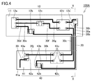
- FIG. 1 is a plan view showing a schematic configuration of an electronic device 100 according to the first embodiment.
- FIG. 2 is a cross-sectional view taken along the line XX of FIG.
- the electronic device 100 is incorporated in various electronic devices such as a portable electronic device such as a wearable portable device and a small sensor, and bears a main or auxiliary function of the electronic device.
- Wearable portable devices include, for example, measuring devices that are worn on clothes and measure body surface temperature, and measuring devices that are wrapped around an arm and measure pulse, blood pressure, and the like.
- the electronic device 100 includes a main body portion 10 where an electronic circuit is formed, a bendable portion 20 that can be bent, and wirings 30 (30a to 30h).
- the main body 10 includes a resin molded body 11 and electronic components 12 (12a to 12e).
- the resin molded body 11 has a substantially plate shape and is made of a resin such as polycarbonate (PC) or acrylonitrile butadiene styrene (ABS).
- the shape of the resin molded body 11 is not particularly limited, and may be appropriately designed according to the shape of the electronic device 100.
- the material of the resin molding 11 may be other types of resin (for example, polypropylene (PP), elastomer, etc.).
- the resin molded body 11 fixes the electronic component 12 by embedding the electronic component 12 (12a to 12e) therein.
- the resin molded body 11 embeds the electronic component 12 so that the electronic component 12 is exposed from the upper surface 11a.
- the electronic component 12 (12a to 12e) is an electronic component such as a chip capacitor, a chip resistor, or an IC (Integrated Circuit).
- the number and kind of electronic components 12 are not particularly limited.
- Electrodes 13a to 13e are formed on the surfaces of the electronic components 12a to 12e exposed from the resin molded body 11, respectively.
- the bending portion 20 is connected to the resin molded body 11 and can be bent. Specifically, the bent portion 20 is made of the same material as the resin molded body 11 and is integrally molded with the resin molded body 11.
- the bent portion 20 has a thickness t1 (for example, 0.2 mm) thinner than the thickness t2 (for example, 3 mm) of the resin molded body 11 so that the flexibility is higher than that of the resin molded body 11.
- the surface of the bent portion 20 includes a continuous surface 20 a that is continuous with the upper surface 11 a of the resin molded body 11.
- continuous of two surfaces means that the step between the two surfaces is small enough that the wiring formed thereon is not cut.
- the continuous surface 20 a of the bent portion 20 is on the same plane as the upper surface 11 a of the resin molded body 11.
- the wiring 30 (30a to 30h) is formed on at least the upper surface 11a of the upper surface 11a of the resin molded body 11 and the continuous surface 20a of the bent portion 20, and is connected to any of the electrodes 13a to 13e of the electronic components 12a to 12e. .
- the wirings 30a to 30c are formed on both the upper surface 11a of the resin molded body 11 and the continuous surface 20a of the bent portion 20, and the electrode 13e of the electronic component 12e, the electrode 13d of the electronic component 12d, and the electronic It is continuously formed from the electrode 13b of the component 12b to the top of the continuous surface 20a.
- the wirings 30 d to 30 h are formed on the upper surface 11 a of the resin molded body 11.
- the wiring 30d is connected to the electrode 13a of the electronic component 12a and the electrode 13b of the electronic component 12b.
- the wiring 30e is connected to the electrode 13a of the electronic component 12a and the electrode 13c of the electronic component 12c.
- the wiring 30f is connected to the electrode 13c of the electronic component 12c and the electrode 13d of the electronic component 12d.
- the wiring 30g is connected to the electrode 13a of the electronic component 12a and the electrode 13d of the electronic component 12d.
- the wiring 30h is connected to the electrode 13d of the electronic component 12d and the electrode 13e of the electronic component 12e.
- the wiring 30 can be easily formed by ejecting silver (Ag) ink using, for example, an ink jet printing method.
- the ink jet printing method is a printing method in which ink is ejected from a nozzle and particulate ink is deposited on a surface to be ejected.
- the wiring 30 can be easily formed by ejecting silver (Ag) ink using an ink jet printing method. Formed.
- FIG. 3 is a diagram illustrating a method for manufacturing the electronic device 100.
- FIGS. 3A to 3D are views for explaining first to fourth steps for manufacturing the electronic device 100, respectively.
- the left side is a plan view and the right side is a side view.
- FIG. 3B shows a cross-sectional view.
- 3C and 3D the left side is a plan view, and the right side is a cross-sectional view taken along line XX in the plan view.
- (First step) As shown in FIG. 3A, first, the electronic components 12a to 12e are temporarily fixed by sticking to the rectangular temporary fixing sheet 200 with an adhesive (not shown). At this time, the electronic components 12a to 12e are attached so that the surfaces on which the electrodes 13a to 13e are formed are in contact with the temporary fixing sheet 200.
- the temporary fixing sheet 200 for example, polyethylene terephthalate (PET), polyethylene naphthalate (PEN), polyphenylene sulfide (PPS), or the like can be used.
- PET polyethylene terephthalate
- PEN polyethylene naphthalate
- PPS polyphenylene sulfide
- the temporary fixing sheet 200 is preferably made of a material that transmits ultraviolet rays and has flexibility for reasons described later.
- the temporary fixing can be performed using, for example, an ultraviolet curable adhesive (not shown) applied to one surface of the temporary fixing sheet 200, for example.
- an ultraviolet curable adhesive is applied to a temporary fixing sheet 200 made of PET having a thickness of 50 ⁇ m to a thickness of 2 to 3 ⁇ m. This application may be performed using a method such as an ink jet printing method.
- the electronic components 12a to 12e are installed at the set positions.
- the adhesive is cured by irradiating UV light having an intensity of, for example, 3000 mJ / cm 2 from the surface of the temporarily fixed sheet 200 on which the electronic components 12a to 12e are not temporarily fixed, thereby temporarily mounting the electronic components 12a to 12e.
- Temporarily fixed to the fixing sheet 200 Temporarily fixed to the fixing sheet 200.
- a mold configured by combining a first mold 210 and a second mold 220 with a temporarily fixed sheet 200 on which electronic components 12a to 12e are temporarily fixed. Install inside.
- a concave portion 211 having the same shape as the temporarily fixed sheet 200 is formed on the surface of the first mold 210 facing the second mold 220, and the temporarily fixed sheet 200 is fitted into the concave portion 211. Thereby, the surface of the temporarily fixed sheet 200 to which the electronic components 12a to 12e are attached faces the second mold 220.
- the depth of the recess 211 is the same as the thickness of the temporarily fixed sheet 200. Therefore, the surface of the temporarily fixed sheet 200 on which the electronic component 12 is temporarily fixed and the surface of the first mold 210 where the concave portion 211 is not formed and the second mold 220 are on the same plane.
- the surface of the second mold 220 that faces the first mold 210 forms a space 221 having a depth t2 in a portion that faces the recess 211 of the first mold 210 and a part that does not face the recess 211 of the first mold 210. It has a shape that forms a space 222 having a depth t1.
- the space 221 and the space 222 communicate with each other.
- a resin material is injected into the spaces 221 and 222 inside the mold configured by combining the first mold 210 and the second mold 220, and resin injection molding is performed.
- the conditions for performing the injection molding may be appropriately selected according to the resin.
- the injection molding is performed at an injection resin temperature of 270 ° C. and an injection pressure of 100 MPa.
- a variety of resin materials can be used as the resin for injection molding. However, if a material having rubber elasticity such as an elastomer is used, the bent portion 20 can be deformed more flexibly. Moreover, the conditions for performing injection molding are not particularly limited.
- the structure 230 obtained by the injection molding in the second step is taken out from the molding die.
- the structure 230 includes the resin molded body 11 having the same shape (thickness t2) as the molding space 221 and the bent portion 20 having the same shape (thickness t1) as the molding space 222.
- the temporary fixing sheet 200 is peeled from the structure 230. Accordingly, the surfaces of the electronic components 12a to 12e are exposed from the sheet bonding surface (corresponding to the upper surface 11a) that is in contact with the temporarily fixed sheet 200 in the resin molded body 11.
- the temporarily fixed sheet 200 is a PET film
- the temporarily fixed sheet 200 is greatly deformed due to a heat change during the second step, and therefore the temporarily fixed sheet 200 can be easily separated from the structure 230.
- a predetermined pattern of wiring 30 (30a to 30h) is formed on the upper surface 11a of the resin molded body 11 and the continuous surface 20a of the bent portion 20. .
- the formation of the wiring 30 can be performed using a method of spraying a conductive material (for example, silver ink or the like) by an inkjet printing method, a method using an aerosol, a method using a dispenser, or the like.
- a conductive material for example, silver ink or the like
- the wiring 30 can be easily formed with a high degree of freedom in circuit design using a method selected as appropriate, and the electronic components 12a to 12e can be electrically connected easily without soldering or the like. it can. Furthermore, industrially, since the electronic components 12a to 12e can be connected after the positions of the electronic components 12a to 12e are determined, for example, compared with the case where the electronic components are aligned with the printed circuit board. The electronic components 12a to 12e can be electrically connected accurately and easily.
- the production of the electronic device 100 including the main body portion 10 including the electronic component 12 and the resin molded body 11, the bending portion 20, and the wiring 30 is completed.
- the electronic device 100 includes the electronic component 12, the resin molded body 11 that embeds and fixes the electronic component 12, and the bendable bending portion 20 that is connected to the resin molded body 11.
- the resin molded body 11 functions as a substrate on which the electronic component is mounted by embedding and fixing the electronic component 12. Thereby, the electronic device 100 can be reduced in size and thickness compared with the case where an electronic component is mounted by solder etc. on the upper surface of the conventional rigid type
- the bent portion 20 is formed integrally with the resin molded body 11. Thereby, since there is no connection point to which a mechanical load is applied between the bent portion 20 and the resin molded body 11, the connection reliability between the resin molded body 11 and the bent portion 20 is increased. Further, since it is not necessary to use a relatively expensive flexible substrate as a separate member, the component cost can be reduced.
- the surface of the resin molded body 11 includes an upper surface (exposed surface) 11 a that exposes the electronic component 12.
- the surface of the bent portion 20 includes a continuous surface 20a continuous with the upper surface 11a.
- the electronic device 100 includes a wiring 30 that is formed on the upper surface 11 a and the continuous surface 20 a and is connected to the electronic component 12. Thereby, the terminal part for electrically connecting a bending part and the resin molding 11 becomes unnecessary, and it can reduce more in size.
- the electronic device 100 is manufactured by the following processes (1) to (3).
- (1) A step of attaching the electronic component 12 to the temporary fixing sheet 200.
- (2) The resin molding 11 in which the electronic component 12 is embedded by disposing the temporary fixing sheet 200 in a molding die (first mold 210 and second mold 220) and filling the molding die with resin;
- (3) Continuous to the upper surface (sheet bonding surface) 11a in contact with the temporarily fixed sheet 200 in the resin molded body 11 and the upper surface 11a in the bent portion 20 exposed by peeling the temporarily fixed sheet 200 from the resin molded body 11. Forming the wiring 30 on the continuous surface 20a.
- the electrical connection between the main body 10 and the bent portion 20 is achieved by forming the wiring 30 on the upper surface 11a of the resin molded body 11 and the continuous surface 20a of the bent portion 20. .
- a complicated process for connecting the flexible substrate to the rigid substrate is unnecessary, and a member such as an adhesive is also unnecessary. Therefore, the manufacturing cost of the electronic device 100 can be reduced.
- the electronic device according to the second embodiment of the present invention is a modification of the electronic device 100 according to the first embodiment, and includes a plurality of main body portions including electronic components and a resin molded body.
- FIG. 4 is a plan view showing a schematic configuration of the electronic device 100A according to the second embodiment.
- FIG. 5 is a cross-sectional view taken along line XX in FIG.
- the electronic device 100A is different from the electronic device 100 of the first embodiment in that the electronic device 100A includes a main body 40 and wirings 30i to 30k.
- the main body 40 is connected to the end of the bent portion 20 opposite to the end connected to the main body 10.
- the main body 40 includes a resin molded body 41 and electronic components 42 (42a to 42c).
- the resin molded body 41 has a substantially plate shape, and is integrally formed with the resin molded body 11 and the bent portion 20 by the same resin as the resin molded body 11 and the bent portion 20.
- the resin molded body 41 fixes the electronic component 42 by embedding the electronic components 42 (42a to 42c) therein.
- the resin molded body 41 has the electronic component 42 embedded so that the electronic component 42 is exposed from the upper surface 41a.
- the upper surface 41a of the resin molded body 41 is continuous with the continuous surface 20a of the bent portion 20, and is on the same plane as the upper surface 11a and the continuous surface 20a of the resin molded body 11.
- the electronic components 42 are electronic components such as a chip capacitor, a chip resistor, and an IC (Integrated Circuit).
- the number and type of electronic components 42 are not particularly limited.
- Electrodes 43a to 43c are formed on the surfaces of the electronic components 42a to 42c exposed from the resin molded body 41, respectively.
- Wirings 30i to 30k are formed on the upper surface 41a of the resin molded body 41 and are connected to the electrodes 43a to 43c of the electronic components 42a to 42c.
- the wirings 30 a to 30 c formed on the continuous surface 20 a of the bent portion 20 are extended to the upper surface 41 a of the resin molded body 41.
- the wiring 30a is connected to the electrode 43b of the electronic component 42b.
- the wirings 30b and 30c are connected to the electrode 43c of the electronic component 42c.
- the electronic device 100A is manufactured by the same method as in the first embodiment. Specifically, in the first step described in the first embodiment, a temporary fixing sheet on which the electronic component 42 is temporarily fixed is prepared separately from the temporary fixing sheet 200 on which the electronic component 12 is temporarily fixed. In the second step, the temporarily fixed sheet 200 on which the electronic component 12 is temporarily fixed and the temporarily fixed sheet on which the electronic component 42 is temporarily fixed are placed inside the mold, and a resin material is injected into the mold. Resin injection molding. Thereby, the resin moldings 11 and 41 and the bent portion 20 are integrally molded.
- the wiring 30 (30a to 30k) is formed on the upper surface 11a of the resin molded body 11, the upper surface 41a of the resin molded body 41, and the continuous surface 20a of the bent portion 20 continuous to the upper surfaces 11a and 41a. May be formed.
- the bendable portion 20 that can be bent is disposed between the plurality of main body portions 10 and 40. Therefore, even when the installation location of the main body 10 and the main body 40 is not on the same plane, the electronic circuit of the main body 10 and the electronic circuit of the main body 40 are electrically connected by the bent portion 20.
- the electronic device 100A can be incorporated into an electronic device while ensuring the state.
- the electronic device according to the third embodiment of the present invention is a modification of the electronic device 100 of the first embodiment or the electronic device 100A of the second embodiment, and the resin molded body 11 and the main body of the bent portion 20 and the main body portion 10.
- the material of the part 40 and the resin molded body 41 is different.
- a resin material having an elongation at break of 150% or less such as polycarbonate (PC) or acrylonitrile butadiene styrene (ABS), is used for the resin molded body 11 of the main body 10 and the resin molded body 41 of the main body 40.
- PC polycarbonate
- ABS acrylonitrile butadiene styrene
- the elongation at break indicates the elongation of the test piece at break relative to the test piece before the test when a tensile test is performed according to JIS K 7162.
- the bending portion 20 has an elongation at break of 300% or more, such as polyurethane (PU) having an elongation at break of 580% or polyamide (PA) having an elongation at break of 300%. It is preferable to use the resin material.
- PU polyurethane
- PA polyamide
- the electronic devices 100 and 100A can be placed in the state in which the bent portion 20 is extended as necessary in accordance with other configurations of the electronic device in which the electronic devices 100 and 100A are incorporated and the positions where the main body portions 10 and 40 are installed. Can be incorporated into. As a result, the electronic devices 100 and 100A can be easily incorporated into the electronic device even if there are individual variations in the internal configuration of the electronic device and some design changes in the internal configuration.
- the bent portion 20 is installed at a position close to a human joint.
- the bending part 20 formed using the resin material whose elongation at break is 300% or more can be expanded and contracted in accordance with the movement of the person wearing the clothes.
- the main body 10 including the temperature sensor as the electronic component 12 is installed at a relatively stable position away from the human joint. It is preferable that the resin molded body 11 of the main body 10 has a certain degree of elasticity in order to reduce irritation to the human when it contacts the human surface.
- the resin material forming the resin molded body 11 is appropriately selected from resin materials whose elongation at break is 150% or less, depending on the installation location of the main body 10.
- the resin constituting the resin molded body 11 and the resin molded body 41 The material is preferably combined with a filler (for example, a glass filler or a carbon filler).
- a filler for example, a glass filler or a carbon filler.
- a conventionally known two-color molding method or the like may be used as a method for differentiating the materials of the bent portion 20, the resin molded body 11 of the main body portion 10, and the resin molded body 41 of the main body portion 40.
- the two-color molding method is a method in which different resins or different materials are combined and molded integrally.
- the resin molded body 11 and the bent portion 20 are integrally molded by molding the resin molded body 11 using the first molding die and then molding the bent portion 20 using the second molding die.
- the resin molded body 11 and the bent portion 20 may be integrally formed by forming the bent portion 20 using the first mold and then forming the resin molded body 11 using the second mold. Good.
- the bent portion 20 When a material having a high elongation at break is used as the bent portion 20, the bent portion 20 may have the same thickness as the resin molded body 11.
- the bent portion 20 is formed by injection molding of a resin material.
- the electronic device according to the fourth embodiment uses a flexible substrate as the bent portion.
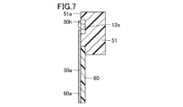
- FIG. 6 is a plan view showing a schematic configuration of an electronic device 100B according to the fourth embodiment.
- FIG. 7 is a cross-sectional view taken along the line XX in FIG.
- the electronic device 100 ⁇ / b> B includes the main body 50 instead of the main body 10, and the electronic device 100 of Embodiment 1 in that it includes a bent portion 60 instead of the bent portion 20. Is different.
- the bent portion 60 is a flexible substrate on a film made of polyimide (PI) or polyethylene terephthalate (PET).
- PI polyimide
- PET polyethylene terephthalate
- the shape of the bending part 60 is not specifically limited, For example, it is a rectangular shape.
- the thickness of the bending part 60 is not specifically limited, For example, it is 50 micrometers.
- the main body 50 is different from the main body 10 of the first embodiment in that a resin molded body 51 is provided instead of the resin molded body 11.
- the resin molded body 51 has a substantially plate shape and is made of a resin such as polycarbonate (PC) or acrylonitrile butadiene styrene (ABS).
- the shape of the resin molded body 51 is not particularly limited, and may be appropriately designed according to the shape of the electronic device 100B.
- the material of the resin molding 51 may be other types of resin (for example, polypropylene (PP), elastomer, etc.).
- the resin molded body 51 fixes the electronic component 12 by embedding the electronic components 12 (12a to 12e) therein.
- the resin molded body 51 embeds the electronic component 12 so that the electronic component 12 is exposed from the upper surface 51a.
- the resin molded body 51 supports the bent portion 60 by embedding a part of the bent portion 60.
- the bent portion 60 is connected to the resin molded body 51.
- the resin molded body 51 embeds and supports an end portion including one short side of the rectangular bent portion 60.
- the resin molded body 51 supports the bent portion 60 such that the upper surface 51a and a part of the surface of the bent portion 60 (continuous surface 60a) are continuous.
- the resin molded body 51 supports the bent portion 60 so that the upper surface 51a and the continuous surface 60a of the bent portion 60 are on the same plane.
- the wiring 30 (30a to 30h) is formed on at least one of the upper surface 51a of the resin molded body 51 and the continuous surface 60a of the bent portion 60 as in the first embodiment, and is attached to any one of the electronic components 12a to 12e. Connecting.
- FIG. 8 is a diagram illustrating a method for manufacturing the electronic device 100B.
- FIGS. 8A to 8D are diagrams for explaining the first to fourth steps for manufacturing the electronic device 100B, respectively.
- the left side is a plan view and the right side is a side view.
- FIG. 8B shows a cross-sectional view.
- 8C and 8D the left side is a plan view, and the right side is a cross-sectional view taken along line XX in the plan view.
- (First step) As shown in FIG. 8A, first, the electronic components 12a to 12e and the bent portion 60 are temporarily fixed by being attached to the temporary fixing sheet 200 with an adhesive. At this time, the electronic components 12a to 12e are attached so that the surfaces on which the electrodes 13a to 13e are formed are in contact with the temporary fixing sheet 200. Only a part of the bent portion 60 is attached to the temporarily fixed sheet 200. Since the method of temporarily fixing the electronic components 12a to 12e and the bent portion 60 to the temporarily fixing sheet 200 is the same as the first step of the first embodiment, detailed description thereof is omitted.
- a temporary fixing sheet 200 in which the electronic components 12a to 12e and the bent portion 60 are temporarily fixed is configured by combining the first mold 210 and the second mold 220. Install inside the mold.
- the temporarily fixing sheet 200 is fitted into the recess 211 formed in the first mold 210.
- the bent portion 60 is accommodated in substantially the entire space 222, and a part of the bent portion 60 protrudes into the space 221.
- a resin material is injected into the space 221 inside the molding die configured by combining the first die 210 and the second die 220, and resin injection molding is performed.
- the conditions for performing injection molding are the same as in the second step of the first embodiment.
- the structure 240 obtained by the injection molding in the second step is taken out from the molding die.
- the structure 240 includes the resin molded body 51 having the same shape as that of the molding die space 221 and the bent portion 60 partially embedded in the resin molded body 51 while embedding the electronic components 12a to 12e.
- the temporary fixing sheet 200 is peeled from the structure 240.
- the surfaces of the electronic components 12a to 12e are exposed from the upper surface 51a of the resin molded body 51.
- the continuous surface 60a that is attached to the temporarily fixing sheet 200 at the bent portion 60 is flush with the upper surface 51a of the resin molded body 51 and is continuous with the upper surface 51a.
- a predetermined pattern of wiring 30 (30a to 30h) is formed on the upper surface 51a of the resin molded body 51 and the continuous surface 60a of the bent portion 60. .
- the method for forming the wiring 30 is the same as that in the fourth step of the first embodiment.
- the production of the electronic device 100B including the main body 50 including the electronic component 12 and the resin molded body 51, the bent portion 60 supported by the resin molded body 51, and the wiring 30 is completed.
- resin molded body 51 embeds and supports a part of bent portion 60. Thereby, compared with the case where it adhere
- the electronic device 100B is manufactured by the following processes (1) to (3).
- the temporary fixing sheet 200 is placed in a mold (a mold in which the first mold 210 and the second mold 220 are combined), and the mold is filled with resin, whereby the electronic component 12 and the bent portion 60 are The process of shape
- the wiring (first wiring) 30 is formed on the upper surface (sheet bonding surface) 51a that is in contact with the temporarily fixing sheet 200 in the resin molded body 51 that is exposed by peeling the temporarily fixed sheet 200 from the resin molded body 51. Process.
- the electronic device 100B including the bent portion 60 can be easily manufactured. Therefore, the manufacturing cost of the electronic device 100B can be reduced.
- the wiring 30 is also formed on the continuous surface 60 a that is continuous with the upper surface 51 a of the resin molded body 51 in the bent portion 60.
- the electrical connection between the main body 50 and the bent portion 60 is achieved by forming the wiring 30 on the upper surface 51 a of the resin molded body 51 and the continuous surface 60 a of the bent portion 60.
- a complicated process for connecting the flexible substrate to the rigid substrate is unnecessary, and a member such as an adhesive is also unnecessary. Therefore, the manufacturing cost of the electronic device 100B can be reduced.
- the electronic device according to the fifth embodiment of the present invention is a modification of the electronic device 100B according to the fourth embodiment, and wiring is previously formed in the bent portion 60 that is a flexible substrate.
- FIG. 9 is a plan view showing a schematic configuration of an electronic device 100C according to the fifth embodiment.
- 10 is a cross-sectional view taken along line XI-XI in FIG.
- the electronic device 100C includes a main body 50, a bent portion 60, and wiring (first wiring) 30 (30d to 30h, 30m, 30n, 30p).
- wiring (second wiring) 61 (61 a to 61 c) is formed in advance on a continuous surface 60 a continuous with the upper surface 51 a of the resin molded body 51.
- the wiring 61 is made of copper having a thickness of about 12 ⁇ m, for example.
- the wiring 61 may be formed of aluminum or the like instead of copper.
- the wiring 30m is formed so as to be connected to the wiring 61a formed on the bent portion 60 and the electronic component 12b.
- the wiring 30n is formed so as to be connected to the wiring 61b formed in the bent portion 60 and the electronic component 12d.
- the wiring 30p is formed so as to connect the wiring 61c formed in the bent portion 60 and the electronic component 12e.
- the electronic device 100C is manufactured by the same manufacturing method (see FIG. 8) as the electronic device 100B of the fourth embodiment.
- the bent portion 60 is attached to the temporarily fixing sheet 200 so that the wiring 61 faces (is in contact with) the temporarily fixing sheet 200.
- the wiring 61 is flush with the upper surface (sheet bonding surface) 51a in contact with the temporarily fixed sheet 200 in the resin molded body 51.
- the wiring 61 of the bending part 60 which is a flexible substrate and the wiring 30 formed on the resin molded body 51 can be easily connected. That is, a complicated process for connecting a flexible substrate to a rigid substrate as in the prior art becomes unnecessary, and a member such as an adhesive becomes unnecessary. Therefore, the manufacturing cost of the electronic device 100C can be reduced.
Landscapes
- Engineering & Computer Science (AREA)
- Microelectronics & Electronic Packaging (AREA)
- Computer Hardware Design (AREA)
- Power Engineering (AREA)
- General Physics & Mathematics (AREA)
- Physics & Mathematics (AREA)
- Condensed Matter Physics & Semiconductors (AREA)
- Manufacturing & Machinery (AREA)
- Structure Of Printed Boards (AREA)
- Encapsulation Of And Coatings For Semiconductor Or Solid State Devices (AREA)
- Structures Or Materials For Encapsulating Or Coating Semiconductor Devices Or Solid State Devices (AREA)
- Production Of Multi-Layered Print Wiring Board (AREA)
- Structures For Mounting Electric Components On Printed Circuit Boards (AREA)
Abstract
La présente invention concerne un dispositif électronique (100) qui comprend un composant électronique (12), un corps moulé en résine (11) dans lequel est intégré et fixé le composant électronique (12), et une partie flexible (20) qui est reliée au corps moulé en résine (11). La partie flexible (20) peut être formée d'un seul tenant avec le corps moulé en résine (11), par exemple. Il s'ensuit de cette configuration qu'il est possible de réduire la taille et l'épaisseur du dispositif électronique (100).
Priority Applications (3)
| Application Number | Priority Date | Filing Date | Title |
|---|---|---|---|
| CN201780060052.XA CN109792836B (zh) | 2016-11-21 | 2017-09-19 | 电子装置及其制造方法 |
| EP17871776.5A EP3544392B1 (fr) | 2016-11-21 | 2017-09-19 | Dispositif électronique et son procédé de fabrication |
| US16/336,923 US11004699B2 (en) | 2016-11-21 | 2017-09-19 | Electronic device and method for manufacturing the same |
Applications Claiming Priority (2)
| Application Number | Priority Date | Filing Date | Title |
|---|---|---|---|
| JP2016226044A JP6776840B2 (ja) | 2016-11-21 | 2016-11-21 | 電子装置およびその製造方法 |
| JP2016-226044 | 2016-11-21 |
Publications (1)
| Publication Number | Publication Date |
|---|---|
| WO2018092407A1 true WO2018092407A1 (fr) | 2018-05-24 |
Family
ID=62146455
Family Applications (1)
| Application Number | Title | Priority Date | Filing Date |
|---|---|---|---|
| PCT/JP2017/033675 WO2018092407A1 (fr) | 2016-11-21 | 2017-09-19 | Dispositif électronique et procédé permettant de produire ce dernier |
Country Status (6)
| Country | Link |
|---|---|
| US (1) | US11004699B2 (fr) |
| EP (1) | EP3544392B1 (fr) |
| JP (1) | JP6776840B2 (fr) |
| CN (1) | CN109792836B (fr) |
| TW (1) | TWI660650B (fr) |
| WO (1) | WO2018092407A1 (fr) |
Families Citing this family (1)
| Publication number | Priority date | Publication date | Assignee | Title |
|---|---|---|---|---|
| EP4247124A1 (fr) * | 2020-11-16 | 2023-09-20 | Fujikura Ltd. | Carte de câblage et procédé de fabrication de carte de câblage |
Citations (7)
| Publication number | Priority date | Publication date | Assignee | Title |
|---|---|---|---|---|
| JPH04346490A (ja) * | 1991-05-24 | 1992-12-02 | Matsushita Electric Ind Co Ltd | プリント配線板の製造方法 |
| JP2006196865A (ja) * | 2004-12-15 | 2006-07-27 | Shinko Electric Ind Co Ltd | 電子部品実装構造体及びその製造方法 |
| JP2009147010A (ja) * | 2007-12-12 | 2009-07-02 | Ricoh Co Ltd | 配線構造体 |
| JP2010062284A (ja) * | 2008-09-03 | 2010-03-18 | Sumitomo Electric Ind Ltd | シール構造および電子機器 |
| JP2011114138A (ja) * | 2009-11-26 | 2011-06-09 | Yaskawa Electric Corp | 半導体装置の製造方法 |
| WO2014185194A1 (fr) * | 2013-05-13 | 2014-11-20 | 株式会社村田製作所 | Carte de circuit imprimé flexible et procédé de production d'une carte de circuit imprimé flexible |
| JP2015207703A (ja) * | 2014-04-22 | 2015-11-19 | オムロン株式会社 | 電子部品を埋設した樹脂構造体およびその製造方法 |
Family Cites Families (17)
| Publication number | Priority date | Publication date | Assignee | Title |
|---|---|---|---|---|
| JPH06177490A (ja) | 1992-12-03 | 1994-06-24 | Matsushita Electric Works Ltd | プリント配線板 |
| JP4103653B2 (ja) | 2003-03-27 | 2008-06-18 | 株式会社デンソー | Icカード |
| EP1643818A4 (fr) * | 2003-07-03 | 2006-08-16 | Hitachi Ltd | Module et procede de fabrication de celui-ci |
| US7759167B2 (en) * | 2005-11-23 | 2010-07-20 | Imec | Method for embedding dies |
| JP4920288B2 (ja) | 2005-12-23 | 2012-04-18 | 帝国通信工業株式会社 | 電子部品の回路基板への取付構造及び取付方法 |
| DE102006055576A1 (de) | 2006-11-21 | 2008-05-29 | Fraunhofer-Gesellschaft zur Förderung der angewandten Forschung e.V. | Verfahren zum Herstellen eines dehnbaren Schaltungsträgers und dehnbarer Schaltungsträger |
| JP5089184B2 (ja) * | 2007-01-30 | 2012-12-05 | ローム株式会社 | 樹脂封止型半導体装置およびその製造方法 |
| JP2009071234A (ja) * | 2007-09-18 | 2009-04-02 | Denso Corp | 半導体装置 |
| TWI355220B (en) | 2008-07-14 | 2011-12-21 | Unimicron Technology Corp | Circuit board structure |
| CN102282661A (zh) * | 2009-01-27 | 2011-12-14 | 松下电工株式会社 | 半导体芯片的安装方法、使用该方法获得的半导体装置以及半导体芯片的连接方法与表面设有布线的立体结构物及其制法 |
| US8929085B2 (en) * | 2011-09-30 | 2015-01-06 | Apple Inc. | Flexible electronic devices |
| JP5386567B2 (ja) * | 2011-11-15 | 2014-01-15 | 株式会社フジクラ | 撮像素子チップの実装方法、内視鏡の組立方法、撮像モジュール及び内視鏡 |
| WO2014002860A1 (fr) * | 2012-06-29 | 2014-01-03 | ソニー株式会社 | Module de caméra et dispositif électronique |
| US20150359099A1 (en) * | 2014-06-04 | 2015-12-10 | Apple Inc. | Low area over-head connectivity solutions to sip module |
| JP6385234B2 (ja) * | 2014-10-16 | 2018-09-05 | 三菱電機株式会社 | 半導体装置 |
| US9778688B2 (en) * | 2014-11-12 | 2017-10-03 | Intel Corporation | Flexible system-in-package solutions for wearable devices |
| JP2016111037A (ja) | 2014-12-02 | 2016-06-20 | 東レ株式会社 | 太陽電池裏面保護用シート、およびそれを用いた太陽電池 |
-
2016
- 2016-11-21 JP JP2016226044A patent/JP6776840B2/ja not_active Expired - Fee Related
-
2017
- 2017-09-19 WO PCT/JP2017/033675 patent/WO2018092407A1/fr active Application Filing
- 2017-09-19 US US16/336,923 patent/US11004699B2/en active Active
- 2017-09-19 EP EP17871776.5A patent/EP3544392B1/fr active Active
- 2017-09-19 CN CN201780060052.XA patent/CN109792836B/zh not_active Expired - Fee Related
- 2017-09-27 TW TW106133028A patent/TWI660650B/zh not_active IP Right Cessation
Patent Citations (7)
| Publication number | Priority date | Publication date | Assignee | Title |
|---|---|---|---|---|
| JPH04346490A (ja) * | 1991-05-24 | 1992-12-02 | Matsushita Electric Ind Co Ltd | プリント配線板の製造方法 |
| JP2006196865A (ja) * | 2004-12-15 | 2006-07-27 | Shinko Electric Ind Co Ltd | 電子部品実装構造体及びその製造方法 |
| JP2009147010A (ja) * | 2007-12-12 | 2009-07-02 | Ricoh Co Ltd | 配線構造体 |
| JP2010062284A (ja) * | 2008-09-03 | 2010-03-18 | Sumitomo Electric Ind Ltd | シール構造および電子機器 |
| JP2011114138A (ja) * | 2009-11-26 | 2011-06-09 | Yaskawa Electric Corp | 半導体装置の製造方法 |
| WO2014185194A1 (fr) * | 2013-05-13 | 2014-11-20 | 株式会社村田製作所 | Carte de circuit imprimé flexible et procédé de production d'une carte de circuit imprimé flexible |
| JP2015207703A (ja) * | 2014-04-22 | 2015-11-19 | オムロン株式会社 | 電子部品を埋設した樹脂構造体およびその製造方法 |
Non-Patent Citations (1)
| Title |
|---|
| See also references of EP3544392A4 * |
Also Published As
| Publication number | Publication date |
|---|---|
| EP3544392A4 (fr) | 2020-01-29 |
| JP2018085377A (ja) | 2018-05-31 |
| US11004699B2 (en) | 2021-05-11 |
| JP6776840B2 (ja) | 2020-10-28 |
| TWI660650B (zh) | 2019-05-21 |
| EP3544392B1 (fr) | 2021-08-11 |
| US20200035511A1 (en) | 2020-01-30 |
| TW201820943A (zh) | 2018-06-01 |
| CN109792836B (zh) | 2021-10-15 |
| EP3544392A1 (fr) | 2019-09-25 |
| CN109792836A (zh) | 2019-05-21 |
Similar Documents
| Publication | Publication Date | Title |
|---|---|---|
| US9922932B2 (en) | Resin structure having electronic component embedded therein, and method for manufacturing said structure | |
| JP5151025B2 (ja) | フレキシブル回路基板 | |
| JP2018120989A (ja) | 樹脂構造体およびその製造方法 | |
| CN106061126B (zh) | 柔性电路的制造方法、柔性电路及含该柔性电路的智能卡 | |
| US9661759B2 (en) | Printed circuit board and method of manufacturing the same | |
| WO2018092407A1 (fr) | Dispositif électronique et procédé permettant de produire ce dernier | |
| CN104768318A (zh) | 软硬结合电路板及其制作方法 | |
| WO2019098029A1 (fr) | Dispositif électronique et son procédé de fabrication | |
| JP7003478B2 (ja) | 電子装置およびその製造方法 | |
| TWI677266B (zh) | 電路結構體以及其製造方法 | |
| JP2009141129A (ja) | フレキシブルプリント配線板およびその製造方法 | |
| JP6406235B2 (ja) | 電子装置及びその製造方法 | |
| JP2018085377A5 (fr) | ||
| CN110024493B (zh) | 电子装置及其制造方法 | |
| WO2018092408A1 (fr) | Dispositif électronique et son procédé de production | |
| JP2007019380A (ja) | 回路配線モジュール及び回路配線モジュールの製造方法 | |
| WO2018163516A1 (fr) | Dispositif électronique et son procédé de fabrication | |
| JP2010157669A (ja) | 電子回路部品および電子機器 |
Legal Events
| Date | Code | Title | Description |
|---|---|---|---|
| 121 | Ep: the epo has been informed by wipo that ep was designated in this application |
Ref document number: 17871776 Country of ref document: EP Kind code of ref document: A1 |
|
| NENP | Non-entry into the national phase |
Ref country code: DE |
|
| WWE | Wipo information: entry into national phase |
Ref document number: 2017871776 Country of ref document: EP |