WO2018088009A1 - 砥粒及びその評価方法並びにウェーハの製造方法 - Google Patents
砥粒及びその評価方法並びにウェーハの製造方法 Download PDFInfo
- Publication number
- WO2018088009A1 WO2018088009A1 PCT/JP2017/032249 JP2017032249W WO2018088009A1 WO 2018088009 A1 WO2018088009 A1 WO 2018088009A1 JP 2017032249 W JP2017032249 W JP 2017032249W WO 2018088009 A1 WO2018088009 A1 WO 2018088009A1
- Authority
- WO
- WIPO (PCT)
- Prior art keywords
- abrasive
- sample
- particle size
- small
- grain
- Prior art date
- Legal status (The legal status is an assumption and is not a legal conclusion. Google has not performed a legal analysis and makes no representation as to the accuracy of the status listed.)
- Ceased
Links
Images




Classifications
-
- H—ELECTRICITY
- H10—SEMICONDUCTOR DEVICES; ELECTRIC SOLID-STATE DEVICES NOT OTHERWISE PROVIDED FOR
- H10P—GENERIC PROCESSES OR APPARATUS FOR THE MANUFACTURE OR TREATMENT OF DEVICES COVERED BY CLASS H10
- H10P90/00—Preparation of wafers not covered by a single main group of this subclass, e.g. wafer reinforcement
- H10P90/12—Preparing bulk and homogeneous wafers
- H10P90/123—Preparing bulk and homogeneous wafers by grinding or lapping
-
- B—PERFORMING OPERATIONS; TRANSPORTING
- B28—WORKING CEMENT, CLAY, OR STONE
- B28D—WORKING STONE OR STONE-LIKE MATERIALS
- B28D5/00—Fine working of gems, jewels, crystals, e.g. of semiconductor material; apparatus or devices therefor
- B28D5/0058—Accessories specially adapted for use with machines for fine working of gems, jewels, crystals, e.g. of semiconductor material
- B28D5/007—Use, recovery or regeneration of abrasive mediums
-
- H—ELECTRICITY
- H10—SEMICONDUCTOR DEVICES; ELECTRIC SOLID-STATE DEVICES NOT OTHERWISE PROVIDED FOR
- H10P—GENERIC PROCESSES OR APPARATUS FOR THE MANUFACTURE OR TREATMENT OF DEVICES COVERED BY CLASS H10
- H10P74/00—Testing or measuring during manufacture or treatment of wafers, substrates or devices
- H10P74/23—Testing or measuring during manufacture or treatment of wafers, substrates or devices characterised by multiple measurements, corrections, marking or sorting processes
-
- B—PERFORMING OPERATIONS; TRANSPORTING
- B24—GRINDING; POLISHING
- B24B—MACHINES, DEVICES, OR PROCESSES FOR GRINDING OR POLISHING; DRESSING OR CONDITIONING OF ABRADING SURFACES; FEEDING OF GRINDING, POLISHING, OR LAPPING AGENTS
- B24B27/00—Other grinding machines or devices
- B24B27/06—Grinders for cutting-off
-
- B—PERFORMING OPERATIONS; TRANSPORTING
- B28—WORKING CEMENT, CLAY, OR STONE
- B28D—WORKING STONE OR STONE-LIKE MATERIALS
- B28D5/00—Fine working of gems, jewels, crystals, e.g. of semiconductor material; apparatus or devices therefor
- B28D5/04—Fine working of gems, jewels, crystals, e.g. of semiconductor material; apparatus or devices therefor by tools other than rotary type, e.g. reciprocating tools
- B28D5/042—Fine working of gems, jewels, crystals, e.g. of semiconductor material; apparatus or devices therefor by tools other than rotary type, e.g. reciprocating tools by cutting with blades or wires mounted in a reciprocating frame
-
- C—CHEMISTRY; METALLURGY
- C09—DYES; PAINTS; POLISHES; NATURAL RESINS; ADHESIVES; COMPOSITIONS NOT OTHERWISE PROVIDED FOR; APPLICATIONS OF MATERIALS NOT OTHERWISE PROVIDED FOR
- C09K—MATERIALS FOR MISCELLANEOUS APPLICATIONS, NOT PROVIDED FOR ELSEWHERE
- C09K3/00—Materials not provided for elsewhere
- C09K3/14—Anti-slip materials; Abrasives
-
- C—CHEMISTRY; METALLURGY
- C09—DYES; PAINTS; POLISHES; NATURAL RESINS; ADHESIVES; COMPOSITIONS NOT OTHERWISE PROVIDED FOR; APPLICATIONS OF MATERIALS NOT OTHERWISE PROVIDED FOR
- C09K—MATERIALS FOR MISCELLANEOUS APPLICATIONS, NOT PROVIDED FOR ELSEWHERE
- C09K3/00—Materials not provided for elsewhere
- C09K3/14—Anti-slip materials; Abrasives
- C09K3/1409—Abrasive particles per se
-
- C—CHEMISTRY; METALLURGY
- C09—DYES; PAINTS; POLISHES; NATURAL RESINS; ADHESIVES; COMPOSITIONS NOT OTHERWISE PROVIDED FOR; APPLICATIONS OF MATERIALS NOT OTHERWISE PROVIDED FOR
- C09K—MATERIALS FOR MISCELLANEOUS APPLICATIONS, NOT PROVIDED FOR ELSEWHERE
- C09K3/00—Materials not provided for elsewhere
- C09K3/14—Anti-slip materials; Abrasives
- C09K3/1454—Abrasive powders, suspensions and pastes for polishing
- C09K3/1463—Aqueous liquid suspensions
-
- H—ELECTRICITY
- H10—SEMICONDUCTOR DEVICES; ELECTRIC SOLID-STATE DEVICES NOT OTHERWISE PROVIDED FOR
- H10P—GENERIC PROCESSES OR APPARATUS FOR THE MANUFACTURE OR TREATMENT OF DEVICES COVERED BY CLASS H10
- H10P52/00—Grinding, lapping or polishing of wafers, substrates or parts of devices
-
- H—ELECTRICITY
- H10—SEMICONDUCTOR DEVICES; ELECTRIC SOLID-STATE DEVICES NOT OTHERWISE PROVIDED FOR
- H10P—GENERIC PROCESSES OR APPARATUS FOR THE MANUFACTURE OR TREATMENT OF DEVICES COVERED BY CLASS H10
- H10P54/00—Cutting or separating of wafers, substrates or parts of devices
-
- H—ELECTRICITY
- H10—SEMICONDUCTOR DEVICES; ELECTRIC SOLID-STATE DEVICES NOT OTHERWISE PROVIDED FOR
- H10P—GENERIC PROCESSES OR APPARATUS FOR THE MANUFACTURE OR TREATMENT OF DEVICES COVERED BY CLASS H10
- H10P74/00—Testing or measuring during manufacture or treatment of wafers, substrates or devices
- H10P74/20—Testing or measuring during manufacture or treatment of wafers, substrates or devices characterised by the properties tested or measured, e.g. structural or electrical properties
Definitions
- the present invention relates to an abrasive and an evaluation method thereof, and more particularly, to an abrasive used in a slicing process using a free abrasive wire saw and an evaluation method thereof. Moreover, this invention relates to the manufacturing method of the wafer including the process of slicing an ingot using the slurry containing such an abrasive grain.
- a slicing process as one of the manufacturing processes of a silicon wafer that is a substrate material of a semiconductor device.
- a wire saw is used.
- a silicon single crystal ingot grown by the CZ method is sliced with a free abrasive wire saw to produce a large number of silicon wafers having a certain thickness.
- Patent Document 1 describes using a slurry in which an abrasive having an average circularity of 0.900 or more and a coolant are mixed.
- Patent Document 2 discloses a method for recovering effective abrasive grains from used slurry, removing worn abrasive grains, and regenerating the slurry by adding new abrasive grains in an amount corresponding to the removed abrasive grains.
- the average circularity of new abrasive grains is in the range of 0.855 to 0.875, the weight ratio of new abrasive grains is about 20%, and the average circularity of abrasive grains contained in the recycled slurry is 0.870 to 0.885. It is described to be in the range.
- Patent Document 3 an additional abrasive grain group is prepared, and a predetermined amount of the additional abrasive grain group is added to and mixed with the abrasive grain group used for the cutting process. It describes that the classification process is performed so that the first abrasive grain size is greater than or equal to the second abrasive grain size. According to this method, the amount of abrasive grains to be discarded can be reduced, and a polishing process having the same quality as that of a new abrasive grain group can be performed.
- Patent Document 4 describes a slurry tank that can be uniformly dispersed in a coolant without agglomeration of abrasive grains. When this slurry tank is used, a slurry free of abrasive aggregates is supplied to the wire saw, so that the slicing operation is stabilized and a wafer having excellent quality stability can be obtained.
- predetermined quality evaluation items such as the grain size distribution and circularity of the abrasive grains are inspected, and only the abrasive grains that meet the quality standards are used. It has been broken.
- an object of the present invention is to provide abrasive grains capable of improving the flatness and stabilizing the processing quality of a wafer sliced by a loose abrasive wire saw, and an evaluation method thereof. Moreover, the objective of this invention is providing the manufacturing method of a wafer including the process of slicing a wafer using the slurry containing such an abrasive grain.
- an abrasive grain evaluation method prepares a predetermined amount of an abrasive grain sample, measures the grain size of each abrasive grain in the abrasive grain sample, and the entire abrasive grain sample.
- the number of small particles is defined by defining the abrasive particles having a particle size equal to or smaller than a predetermined reference particle size smaller than the average particle size of the abrasive sample as a small particle, and the abrasive sample A small particle ratio that is the number ratio of the small particles to the whole is calculated, and it is determined whether the small particle ratio is equal to or less than a predetermined threshold value.
- the present invention it is possible to eliminate the cause of deteriorating the flatness of the wafer by evaluating the amount of small particles contained in the entire abrasive grains by the number ratio, thereby improving the quality of wafer slicing processing and Stabilization can be achieved.
- the abrasive grain evaluation method measures the particle size distribution in the volume count of the abrasive grain sample from the grain size of each abrasive grain in the abrasive grain sample, and the average grain size of the abrasive grain sample from the grain size distribution.
- the diameter is calculated, and it is preferable to define the abrasive grains distributed in a region of a reference particle size smaller than the average particle size as the small particles. Further, the reference particle size is preferably 1 ⁇ 2 of the average particle size. According to this, a small particle can be defined clearly and easily.
- the threshold is preferably 50%. If the small particle ratio of the abrasive grains is 50% or less, a wafer with good flatness can be produced, and the processing quality of the wafer can be stabilized.
- the abrasive sample when the small particle ratio is less than or equal to the threshold, it is determined that the abrasive sample can be used for slicing an ingot by a wire saw, and when the small particle ratio is larger than the threshold, It is preferable to determine that the abrasive grain sample cannot be used for the slicing.
- the abrasive grain according to the present invention measures the grain size of each abrasive grain in the abrasive grain sample, counts the total number of the abrasive grain samples, and has a predetermined reference smaller than the average grain diameter of the abrasive grain sample.
- the small particle ratio which is the number ratio of the small particles to the entire abrasive sample, is 50% or less. It is characterized by that.
- ADVANTAGE OF THE INVENTION According to this invention, the wafer with favorable flatness can be manufactured in the slice processing of the ingot using a wire saw, and stabilization of the processing quality of a wafer can be aimed at.
- the method for producing a wafer according to the present invention is characterized by including a slicing step of slicing an ingot using a free abrasive wire saw together with the slurry containing the abrasive grains of the present invention having the above characteristics. According to the present invention, a wafer with good flatness can be manufactured, and the processing quality of the wafer can be stabilized.
- the method for manufacturing a wafer according to the present invention includes an inspection process for inspecting the quality of abrasive grains, and a slicing process for slicing an ingot using a free abrasive wire saw together with a slurry containing abrasive grains that have passed the inspection.
- the inspection step includes a small particle rate inspection step of inspecting a small particle rate of the abrasive grains, and in the small particle rate inspection step, a predetermined amount of an abrasive sample is prepared, and each of the abrasive sample samples Measuring the particle size of the abrasive grains, counting the total number of the abrasive grain samples, and reducing the abrasive grains having a grain size equal to or smaller than a predetermined reference grain size smaller than the average grain diameter of the abrasive grain samples to the small particles
- the number of the small particles is defined, and the small particle ratio that is the ratio of the number of the small particles to the whole abrasive sample is calculated to determine whether the small particle ratio is equal to or less than a predetermined threshold value. Characterized in that it. According to the present invention, a wafer with good flatness can be manufactured, and the processing quality of the wafer can be stabilized.
- an abrasive grain capable of improving the flatness of a wafer sliced by a free abrasive wire saw and stabilizing the processing quality, and an evaluation method thereof.
- the manufacturing method of a wafer including the process of slicing a wafer using the slurry containing such an abrasive grain can be provided.
- FIG. 1 is a flowchart illustrating a method for manufacturing a silicon wafer.
- FIG. 2 is a perspective view schematically showing the configuration of the loose abrasive wire saw.
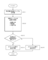
- FIG. 3 is a flowchart schematically showing an abrasive grain inspection process.
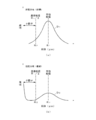
- FIG. 4 is a particle size distribution diagram of abrasive grains for explaining a method of calculating a small particle ratio.
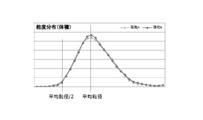
- FIG. 5 is a graph showing the particle size distribution of the abrasive grain samples A and B by volume count.
- FIG. 6 is a graph showing the particle size distribution of the abrasive grain samples A and B in the number count.
- FIG. 7 is a graph (box whisker plot) showing the flatness (GBIR) of a wafer sliced using the abrasive grain samples C1 to C5.
- FIG. 1 is a flowchart for explaining a method of manufacturing a silicon wafer.
- the silicon wafer is formed on a silicon single crystal ingot by peripheral grinding S11, slice S12, lapping S13, etching S14, double-side polishing (rough polishing) S15, single-side polishing (mirror polishing) S16, cleaning S17, and the like.
- the slicing step S12 is a step of slicing a silicon single crystal ingot using a loose abrasive wire saw, whereby a large number of silicon wafers having a certain thickness are produced.
- FIG. 2 is a perspective view schematically showing the structure of the loose abrasive wire saw.
- the loose abrasive wire saw 1 is a so-called multi-wire saw, and is composed of three main rollers 10A, 10B, 10C parallel to each other and one wire 11 between the main rollers 10A, 10B, 10C.
- a wire row 11R formed at a constant pitch between the main rollers 10A and 10B
- slurry nozzles 20A and 20B for supplying slurry to the wire row 11R
- an elevator 18 for the silicon single crystal ingot 2
- a large number of annular grooves are formed on the outer peripheral surfaces of the main rollers 10A, 10B, and 10C at a constant pitch, and a wire row 11R is formed by winding the wires 11 while being fitted into the grooves.
- the wire row 11R reciprocates between the main rollers 10A and 10B by the rotation of the main rollers 10A, 10B, and 10C, and the ingot 2 is cut by pressing the ingot 2 against the wire row 11R.
- One reel 12A is a wire supply reel on which a new wire is wound
- the other reel 12B is a wire collection reel that winds up a used wire. After the wire 11 is fed from one reel 12A, the wire 11 is repeatedly wound around the main rollers 10A, 10B, and 10C in this order via a plurality of guide rollers 13, and the other passes again via the plurality of guide rollers 13. The reel 12B is wound up.
- a tension adjusting mechanism 14A is provided on the travel path of the wire 11 between one reel 12A and the main roller 10A, and on the travel path of the wire 11 between the other reel 12B and the main roller 10C.
- a tension adjusting mechanism 14B is provided.
- Each of the tension adjusting mechanisms 14A and 14B includes a dancer roller 15 around which the wire 11 is wound, a dancer arm 16 that rotatably supports the dancer roller 15, and an actuator 17 that supports the dancer arm 16. An appropriate tension is applied to the wire 11 using the driving force of the actuator 17.
- the wire 11 reciprocates in the direction from one reel 12A to the other reel 12B or in the opposite direction, but the amount of wire 11 delivered from the reel 12A should be greater than the amount of wire 11 delivered from the reel 12B.
- the core wire can be gradually supplied.
- the reels 12A and 12B are driven by a torque motor (not shown).
- Slurry is supplied from the slurry nozzles 20A and 20B to the wire row 11R being cut.
- the slurry is supplied from a slurry tank (not shown) to the slurry nozzles 20A and 20B through a pipe.
- the slurry nozzles 20A and 20B have a large number of nozzle holes located above the wires 11 of the wire row 11R, and the slurry discharged from the nozzle holes flows down in a curtain shape and the wires of the wire row 11R in the running state. Be put on.
- the slurry adhering to the wire 11 reaches the processing point of the ingot together with the traveling wire 11, whereby the ingot is cut.
- the slurry is obtained by dispersing abrasive grains in a water-soluble or oil-based coolant, and the material of the abrasive grains is preferably SiC or Al 2 O 3 , and the coolant is preferably a glycol type.
- the abrasive grains In order to ensure the processing quality of the wafer in the slicing step S12, the abrasive grains must satisfy a certain quality standard. Therefore, the quality inspection of the abrasive grains is performed before the abrasive grains are actually used in the slicing step S12.
- FIG. 3 is a flowchart schematically showing the abrasive grain inspection process.
- a predetermined amount of abrasive grain sample extracted from the abrasive grain lot is prepared (step S21), and the quality of the abrasive grain sample is inspected (step S22).
- quality evaluation items include “particle size distribution”, “circularity”, and “small particle ratio” of abrasive grains.
- small particle ratio is an index indicating the ratio (number ratio) of small particles (fine particles) in the abrasive sample, and has been inspected as a quantitative index so far. It was an item that did not exist. Small particles not only contribute to cutting of the ingot, but also contribute to the cutting, which is a hindrance to the cutting of medium-sized abrasive grains. This is a factor that deteriorates the flatness of the wafer. However, when the small particle ratio is kept below a certain level, the flatness of the wafer after slicing can be improved, and the processing quality of the wafer can be stabilized.
- the particle size of the small particles is preferably 1/2 or less of the average particle size of the particle size distribution in the volume count of the abrasive sample.
- the quality of the abrasive grains can be stabilized and the processing quality of the wafer can be improved.
- the reference particle size for determining whether or not the particle size is smaller than 1/2 of the average particle size of the particle size distribution, the definition of the small particle becomes clear and the reference particle size can be easily determined based on the particle size distribution
- the small particles that can be set and affect the processing quality of the wafer can be easily identified.
- the small particle ratio of the abrasive grains is preferably 50% or less. If the small particle ratio is 50% or less, the flatness of the wafer after slicing can be improved substantially, and the processing quality of the wafer can be stabilized, but if it exceeds 50%, the flatness of the wafer deteriorates. This is because the wafer does not meet the predetermined quality standard.
- FIG. 4 is a particle size distribution diagram of abrasive grains for explaining a method of calculating a small particle ratio.
- the small particle ratio it is first to measure the particle diameter of the individual abrasive grains of the abrasive grain samples, determine a particle size distribution D 1 of the in abrasive entire sample volume count as shown in Figure 4 (a).
- the method for measuring the individual particle size of the abrasive sample is not particularly limited. For example, the abrasive particles are photographed one by one with a camera while flowing the liquid containing the abrasive particles in the flow path between the thin glass cells, and image processing is performed. By doing so, the particle size of each abrasive grain can be measured.
- the number of small particles having a particle size equal to or less than 1 ⁇ 2 of the average particle size R 1 is counted based on the particle size distribution D 2 by counting the number of abrasive samples as shown in FIG.
- the small particle ratio which is the ratio of the number of small particles to the entire abrasive sample, is calculated.
- the threshold for the small particle ratio is preferably 50% or less. This is because if the small particle ratio exceeds 50%, the flatness index of the silicon wafer such as GBIR (Global Backside, Ideal, Focal, Plane, Range), Warp, and nanotopography deteriorates, and the predetermined quality standard is not satisfied.
- the evaluation method of the abrasive grain according to the present embodiment by measuring the particle size distribution D 1 of the in abrasive entire sample volume basis, 1/2 or less of the average particle diameter R 1 of the particle size distribution D 1 The number of small particles distributed in the region is counted, and it is determined whether the small particle ratio, which is the ratio of the number of small particles to the total number of abrasive samples, is 50% or less. Since the ingot slicing process is performed using the slurry containing the abrasive grains, the flatness of the wafer cut by the free abrasive wire saw can be improved and the processing quality of the wafer can be stabilized.
- the value of 1/2 of the average particle size of the particle size distribution in the volume count of the abrasive sample is set as the reference particle size, but is not necessarily limited to 1/2. Moreover, it is also possible to set a value of 1 ⁇ 2 of the average particle size of the particle size distribution in the count of the number of abrasive sample as the reference particle size.
- abrasive grain samples A and B respectively extracted from different lots were prepared, and the particle size distribution by volume count and the particle size distribution by number count of these abrasive grain samples were measured.
- a particle size / shape analyzer FPIA-3000 manufactured by Sysmex Corporation was used for measuring the particle size of individual abrasive grains in the abrasive sample.
- FIG. 5 is a graph showing the particle size distribution in the volume counts of the abrasive samples A and B, where the horizontal axis indicates the abrasive size ( ⁇ m) and the vertical axis indicates the frequency (volume ratio). As apparent from the graph of FIG. 5, there was almost no difference in the particle size distribution of the abrasive samples A and B when the volume was counted.
- FIG. 6 is a graph showing the particle size distribution in the number count of the abrasive samples A and B, where the horizontal axis indicates the abrasive size ( ⁇ m) and the vertical axis indicates the frequency (number ratio).
- the abrasive grain sample B contained much more fine particles than the abrasive grain sample A.
- the presence of small particles hardly visible in the particle size distribution by volume count (FIG. 5) can be easily confirmed by the particle size distribution by number count (FIG. 6).
- the small particle ratio of the abrasive grain samples A and B was measured, the small particle ratio of the abrasive grain sample A was 10%, and the small particle ratio of the abrasive grain sample B was 70%.
- abrasive grains samples C1 to C5 having different small particle ratios were prepared.
- the small particle ratios of the abrasive samples C1 to C5 were 10%, 30%, 50%, 70%, and 90%, respectively.
- a silicon single crystal ingot was sliced with a wire saw.
- GBIR which is a flatness index of the obtained wafer, was measured.
- GBIR is a global flatness index based on the back surface, and is defined as a deviation between the maximum thickness and the minimum thickness of the wafer surface with respect to the reference surface when the back surface of the wafer is used as a reference surface.
- FIG. 7 is a graph (box-and-whisker plot) showing GBIR of wafers sliced using abrasive grain samples C1 to C5, the horizontal axis is the small particle ratio (%), and the vertical axis is GBIR (standard value). .
- the GBIR of the abrasive sample C1 having a small particle rate of 10% and the abrasive sample C2 having a small particle rate of 30% was low, but the GBIR of the abrasive sample C3 having a small particle rate of 50% was slightly higher. It was.
- the GBIR of the abrasive grain sample C4 having a small particle ratio of 70% and the abrasive grain sample C5 having a 90% particle ratio was further increased, and the symptoms of poor cutting were confirmed. From the above results, it was found that if the abrasive grain has a small particle ratio of 50% or less, the flatness of the wafer can be improved.
Landscapes
- Chemical & Material Sciences (AREA)
- Engineering & Computer Science (AREA)
- Materials Engineering (AREA)
- Organic Chemistry (AREA)
- Mechanical Engineering (AREA)
- Mechanical Treatment Of Semiconductor (AREA)
- Finish Polishing, Edge Sharpening, And Grinding By Specific Grinding Devices (AREA)
- Manufacturing & Machinery (AREA)
Abstract
Description
2 シリコン単結晶インゴット
10A,10B,10C メインローラ
11 ワイヤ
11R ワイヤ列
12A,12B リール
13 ガイドローラ
14A,14B 張力調整機構
15 ダンサーローラ
16 ダンサーアーム
17 アクチュエータ
18 昇降装置
20A,20B スラリーノズル
D1 砥粒サンプルの粒度分布(体積カウント)
D2 砥粒サンプルの粒度分布(個数カウント)
R1 粒度分布D1の平均粒径
R2 基準粒径(R1/2)
S11 外周研削
S12 スライス
S13 ラッピング
S14 エッチング
S15 両面研磨
S16 片面研磨
S17 洗浄
Claims (8)
- 所定量の砥粒サンプルを用意し、
前記砥粒サンプル中の個々の砥粒の粒径を測定すると共に、前記砥粒サンプル全体の個数をカウントし、
前記砥粒サンプルの平均粒径よりも小さい所定の基準粒径以下の粒径を有する砥粒を小粒子と定義して当該小粒子の個数をカウントし、
前記砥粒サンプル全体に対する前記小粒子の個数比である小粒子率を算出し、
前記小粒子率が所定の閾値以下であるかどうかを判断することを特徴とする砥粒の評価方法。 - 前記砥粒サンプル中の個々の砥粒の粒径から前記砥粒サンプルの体積カウントでの粒度分布を測定し、前記粒度分布から前記砥粒サンプルの平均粒径を算出し、前記平均粒径よりも小さい基準粒径以下の領域に分布する砥粒を前記小粒子と定義する、請求項1に記載の砥粒の評価方法。
- 前記基準粒径は前記平均粒径の1/2である、請求項1又は2に記載の砥粒の評価方法。
- 前記閾値は50%である、請求項1乃至3のいずれか一項に記載の砥粒の評価方法。
- 前記小粒子率が前記閾値以下である場合には、ワイヤソーによるインゴットのスライス加工に前記砥粒サンプルを使用可能と判断し、
前記小粒子率が前記閾値よりも大きい場合には、前記スライス加工に前記砥粒サンプルを使用不可と判断する、請求項1乃至4のいずれか一項に記載の砥粒の評価方法。 - 砥粒サンプル中の個々の砥粒の粒径を測定すると共に、前記砥粒サンプル全体の個数をカウントし、前記砥粒サンプルの平均粒径よりも小さい所定の基準粒径以下の粒径を有する砥粒を小粒子と定義して当該小粒子の個数をカウントしたとき、前記砥粒サンプル全体に対する前記小粒子の個数比である小粒子率が50%以下であることを特徴とする砥粒。
- 請求項6に記載の砥粒を含むスラリーと共に遊離砥粒ワイヤソーを用いてインゴットをスライス加工するスライス工程を含むことを特徴とするウェーハの製造方法。
- 砥粒の品質を検査する検査工程と、
前記検査をパスした砥粒を含むスラリーと共に遊離砥粒ワイヤソーを用いてインゴットをスライス加工するスライス工程とを備え、
前記検査工程は、前記砥粒の小粒子率を検査する小粒子率検査工程を含み、
前記小粒子率検査工程では、
所定量の砥粒サンプルを用意し、
前記砥粒サンプル中の個々の砥粒の粒径を測定すると共に、前記砥粒サンプル全体の個数をカウントし、
前記砥粒サンプルの平均粒径よりも小さい所定の基準粒径以下の粒径を有する砥粒を前記小粒子として定義して当該小粒子の個数をカウントし、
前記砥粒サンプル全体に対する前記小粒子の個数比である前記小粒子率を算出し、
前記小粒子率が所定の閾値以下であるかどうかを判断することを特徴とするウェーハの製造方法。
Priority Applications (4)
| Application Number | Priority Date | Filing Date | Title |
|---|---|---|---|
| KR1020197011932A KR102222836B1 (ko) | 2016-11-10 | 2017-09-07 | 지립 및 그의 평가 방법 그리고 웨이퍼의 제조 방법 |
| CN201780069847.7A CN109952172B (zh) | 2016-11-10 | 2017-09-07 | 磨粒与其评价方法以及晶片的制造方法 |
| US16/348,345 US11373858B2 (en) | 2016-11-10 | 2017-09-07 | Abrasive grains, evaluation method therefor, and wafer manufacturing method |
| DE112017005669.1T DE112017005669B4 (de) | 2016-11-10 | 2017-09-07 | Schleifkörner, beurteilungsverfahren dafür und waferherstellungsverfahren |
Applications Claiming Priority (2)
| Application Number | Priority Date | Filing Date | Title |
|---|---|---|---|
| JP2016219393A JP6604313B2 (ja) | 2016-11-10 | 2016-11-10 | 砥粒の評価方法並びにウェーハの製造方法 |
| JP2016-219393 | 2016-11-10 |
Publications (1)
| Publication Number | Publication Date |
|---|---|
| WO2018088009A1 true WO2018088009A1 (ja) | 2018-05-17 |
Family
ID=62109500
Family Applications (1)
| Application Number | Title | Priority Date | Filing Date |
|---|---|---|---|
| PCT/JP2017/032249 Ceased WO2018088009A1 (ja) | 2016-11-10 | 2017-09-07 | 砥粒及びその評価方法並びにウェーハの製造方法 |
Country Status (7)
| Country | Link |
|---|---|
| US (1) | US11373858B2 (ja) |
| JP (1) | JP6604313B2 (ja) |
| KR (1) | KR102222836B1 (ja) |
| CN (1) | CN109952172B (ja) |
| DE (1) | DE112017005669B4 (ja) |
| TW (1) | TWI646493B (ja) |
| WO (1) | WO2018088009A1 (ja) |
Families Citing this family (6)
| Publication number | Priority date | Publication date | Assignee | Title |
|---|---|---|---|---|
| JP7003897B2 (ja) * | 2018-11-16 | 2022-02-04 | 株式会社Sumco | ウェーハの製造方法、ワイヤーソー用再利用スラリーの品質評価方法、及びワイヤーソー用使用済みスラリーの品質評価方法 |
| DE102018221922A1 (de) * | 2018-12-17 | 2020-06-18 | Siltronic Ag | Verfahren zur Herstellung von Halbleiterscheiben mittels einer Drahtsäge, Drahtsäge und Halbleiterscheibe aus einkristallinem Silizium |
| WO2023053476A1 (ja) * | 2021-09-30 | 2023-04-06 | 有限会社サクセス | 半導体結晶ウェハの製造方法および製造装置 |
| JP7007625B1 (ja) * | 2021-09-30 | 2022-01-24 | 有限会社サクセス | 半導体結晶ウェハの製造方法および製造装置 |
| JP7041931B1 (ja) * | 2021-12-20 | 2022-03-25 | 有限会社サクセス | 半導体結晶ウェハの製造方法および製造装置 |
| CN117382007A (zh) * | 2022-07-04 | 2024-01-12 | 隆基绿能科技股份有限公司 | 一种切割线表面的颗粒及其制备方法、切割线及切割装置 |
Citations (6)
| Publication number | Priority date | Publication date | Assignee | Title |
|---|---|---|---|---|
| JP2002338952A (ja) * | 2001-05-11 | 2002-11-27 | Ishizuka Kenkyusho:Kk | ダイヤモンド粒子研磨材 |
| JP2005039174A (ja) * | 2002-11-28 | 2005-02-10 | Kyocera Corp | 砥粒およびそれを用いた半導体ブロックのスライス方法 |
| JP2015223674A (ja) * | 2014-05-28 | 2015-12-14 | 信越半導体株式会社 | 固定砥粒ワイヤ及びワイヤソー並びにワークの切断方法 |
| JP2016124055A (ja) * | 2014-12-26 | 2016-07-11 | 株式会社Sumco | 砥粒の評価方法、および、シリコンウェーハの製造方法 |
| WO2016117559A1 (ja) * | 2015-01-19 | 2016-07-28 | 株式会社フジミインコーポレーテッド | 研磨用組成物 |
| WO2016117560A1 (ja) * | 2015-01-19 | 2016-07-28 | 株式会社フジミインコーポレーテッド | 変性コロイダルシリカおよびその製造方法、並びにこれを用いた研磨剤 |
Family Cites Families (15)
| Publication number | Priority date | Publication date | Assignee | Title |
|---|---|---|---|---|
| US5710069A (en) * | 1996-08-26 | 1998-01-20 | Motorola, Inc. | Measuring slurry particle size during substrate polishing |
| JP4212155B2 (ja) | 1998-08-20 | 2009-01-21 | 株式会社スーパーシリコン研究所 | ワイヤソー用スラリータンク |
| JP3669557B2 (ja) * | 1999-04-27 | 2005-07-06 | 三菱住友シリコン株式会社 | ワイヤソー用スラリー |
| JP2001300844A (ja) * | 2000-04-21 | 2001-10-30 | Nec Corp | スラリー供給装置及びその供給方法 |
| JP3655811B2 (ja) * | 2000-07-21 | 2005-06-02 | 株式会社石塚研究所 | 単結晶質ダイヤモンド微粉 |
| CN1239303C (zh) * | 2002-11-28 | 2006-02-01 | 京瓷株式会社 | 磨粒及用该磨粒的半导体块的切片方法 |
| CN100368502C (zh) * | 2002-11-28 | 2008-02-13 | 京瓷株式会社 | 磨粒及用该磨粒的半导体块的切片方法 |
| JP4248895B2 (ja) | 2003-02-27 | 2009-04-02 | Sumco Techxiv株式会社 | スラリ再生方法及びワイヤソーシステム |
| JP4311247B2 (ja) * | 2004-03-19 | 2009-08-12 | 日立電線株式会社 | 研磨用砥粒、研磨剤、研磨液の製造方法 |
| KR100630691B1 (ko) * | 2004-07-15 | 2006-10-02 | 삼성전자주식회사 | 산화세륨 연마 입자 및 그 제조 방법과 cmp용 슬러리조성물 및 그 제조 방법과 이들을 이용한 기판 연마 방법 |
| FR2927272B1 (fr) * | 2008-02-07 | 2010-05-21 | Saint Gobain Ct Recherches | Poudre de grains abrasifs. |
| JP5526960B2 (ja) | 2010-04-13 | 2014-06-18 | 株式会社Sumco | 再生砥粒群生成方法、ウェーハ製造システム、及びウェーハ製造方法 |
| JP5594273B2 (ja) | 2011-10-27 | 2014-09-24 | 信越半導体株式会社 | スラリー及びスラリーの製造方法 |
| JP2013217694A (ja) * | 2012-04-05 | 2013-10-24 | Hitachi Chemical Co Ltd | 化学機械研磨スラリーの砥粒のヤング率測定方法 |
| WO2015046090A1 (ja) * | 2013-09-26 | 2015-04-02 | 株式会社フジミインコーポレーテッド | 研磨用組成物、研磨用組成物の製造方法およびシリコンウェーハ製造方法 |
-
2016
- 2016-11-10 JP JP2016219393A patent/JP6604313B2/ja active Active
-
2017
- 2017-09-07 TW TW106130604A patent/TWI646493B/zh active
- 2017-09-07 CN CN201780069847.7A patent/CN109952172B/zh active Active
- 2017-09-07 US US16/348,345 patent/US11373858B2/en active Active
- 2017-09-07 KR KR1020197011932A patent/KR102222836B1/ko active Active
- 2017-09-07 WO PCT/JP2017/032249 patent/WO2018088009A1/ja not_active Ceased
- 2017-09-07 DE DE112017005669.1T patent/DE112017005669B4/de active Active
Patent Citations (6)
| Publication number | Priority date | Publication date | Assignee | Title |
|---|---|---|---|---|
| JP2002338952A (ja) * | 2001-05-11 | 2002-11-27 | Ishizuka Kenkyusho:Kk | ダイヤモンド粒子研磨材 |
| JP2005039174A (ja) * | 2002-11-28 | 2005-02-10 | Kyocera Corp | 砥粒およびそれを用いた半導体ブロックのスライス方法 |
| JP2015223674A (ja) * | 2014-05-28 | 2015-12-14 | 信越半導体株式会社 | 固定砥粒ワイヤ及びワイヤソー並びにワークの切断方法 |
| JP2016124055A (ja) * | 2014-12-26 | 2016-07-11 | 株式会社Sumco | 砥粒の評価方法、および、シリコンウェーハの製造方法 |
| WO2016117559A1 (ja) * | 2015-01-19 | 2016-07-28 | 株式会社フジミインコーポレーテッド | 研磨用組成物 |
| WO2016117560A1 (ja) * | 2015-01-19 | 2016-07-28 | 株式会社フジミインコーポレーテッド | 変性コロイダルシリカおよびその製造方法、並びにこれを用いた研磨剤 |
Also Published As
| Publication number | Publication date |
|---|---|
| KR20190051064A (ko) | 2019-05-14 |
| DE112017005669B4 (de) | 2025-03-27 |
| TWI646493B (zh) | 2019-01-01 |
| KR102222836B1 (ko) | 2021-03-03 |
| CN109952172B (zh) | 2021-09-24 |
| TW201826206A (zh) | 2018-07-16 |
| US11373858B2 (en) | 2022-06-28 |
| US20200058484A1 (en) | 2020-02-20 |
| JP2018075668A (ja) | 2018-05-17 |
| JP6604313B2 (ja) | 2019-11-13 |
| DE112017005669T5 (de) | 2019-08-08 |
| CN109952172A (zh) | 2019-06-28 |
Similar Documents
| Publication | Publication Date | Title |
|---|---|---|
| JP6604313B2 (ja) | 砥粒の評価方法並びにウェーハの製造方法 | |
| CN108140593B (zh) | 缺陷区域的判定方法 | |
| JP6172053B2 (ja) | 固定砥粒ワイヤ及びワイヤソー並びにワークの切断方法 | |
| JP2006130636A (ja) | ワイヤソー | |
| JP4537643B2 (ja) | シリコン単結晶ウェーハの製造方法 | |
| JP3651440B2 (ja) | シリコンウェーハの評価方法及びそのエッチング液 | |
| JP4383149B2 (ja) | 砥粒およびそれを用いた半導体ブロックのスライス方法 | |
| JP6233296B2 (ja) | 砥粒の評価方法、および、シリコンウェーハの製造方法 | |
| JP6011930B2 (ja) | シリコンウェーハの評価方法及びそのエッチング液 | |
| JP7172878B2 (ja) | 単結晶シリコンの抵抗率測定方法 | |
| TWI731428B (zh) | 晶圓的製造方法、線鋸用再利用漿料的品質評估方法、及線鋸用已使用之漿料的品質評估方法 | |
| CN100368502C (zh) | 磨粒及用该磨粒的半导体块的切片方法 | |
| Lottspeich et al. | A novel approach to determine the diamond occupancy of diamond wires for optimized cutting processes for crystalwire silicon | |
| WO2026062957A1 (ja) | ウェーハの製造方法 | |
| JP2021040006A (ja) | 単結晶シリコンの酸素濃度又は炭素濃度の測定方法 |
Legal Events
| Date | Code | Title | Description |
|---|---|---|---|
| 121 | Ep: the epo has been informed by wipo that ep was designated in this application |
Ref document number: 17869283 Country of ref document: EP Kind code of ref document: A1 |
|
| ENP | Entry into the national phase |
Ref document number: 20197011932 Country of ref document: KR Kind code of ref document: A |
|
| 122 | Ep: pct application non-entry in european phase |
Ref document number: 17869283 Country of ref document: EP Kind code of ref document: A1 |
|
| WWG | Wipo information: grant in national office |
Ref document number: 112017005669 Country of ref document: DE |