WO2018079477A1 - 多層基板およびその製造方法 - Google Patents
多層基板およびその製造方法 Download PDFInfo
- Publication number
- WO2018079477A1 WO2018079477A1 PCT/JP2017/038165 JP2017038165W WO2018079477A1 WO 2018079477 A1 WO2018079477 A1 WO 2018079477A1 JP 2017038165 W JP2017038165 W JP 2017038165W WO 2018079477 A1 WO2018079477 A1 WO 2018079477A1
- Authority
- WO
- WIPO (PCT)
- Prior art keywords
- base material
- interlayer connection
- multilayer substrate
- connection conductor
- gas
- Prior art date
- Legal status (The legal status is an assumption and is not a legal conclusion. Google has not performed a legal analysis and makes no representation as to the accuracy of the status listed.)
- Ceased
Links
Images



Classifications
-
- H—ELECTRICITY
- H05—ELECTRIC TECHNIQUES NOT OTHERWISE PROVIDED FOR
- H05K—PRINTED CIRCUITS; CASINGS OR CONSTRUCTIONAL DETAILS OF ELECTRIC APPARATUS; MANUFACTURE OF ASSEMBLAGES OF ELECTRICAL COMPONENTS
- H05K1/00—Printed circuits
- H05K1/02—Details
- H05K1/03—Use of materials for the substrate
-
- H—ELECTRICITY
- H05—ELECTRIC TECHNIQUES NOT OTHERWISE PROVIDED FOR
- H05K—PRINTED CIRCUITS; CASINGS OR CONSTRUCTIONAL DETAILS OF ELECTRIC APPARATUS; MANUFACTURE OF ASSEMBLAGES OF ELECTRICAL COMPONENTS
- H05K3/00—Apparatus or processes for manufacturing printed circuits
- H05K3/46—Manufacturing multilayer circuits
Definitions
- the present invention relates to a multilayer substrate formed by laminating insulating substrates and a method for manufacturing the same.
- gas may be released from a portion that becomes an interlayer connection conductor after heating. If this gas remains in the multilayer substrate, there is a problem that reliability is lowered and it is difficult to obtain predetermined electrical characteristics.
- Patent Document 1 in order to release the gas released from the portion that becomes the interlayer connection conductor after heating in the base material laminating step in the base material laminating direction, a plurality of minute gas vents are formed on the ground conductor pattern having a large area. It is described that a hole is provided.
- the gas released from the portion that becomes the interlayer connection conductor after heating is a minute gas formed in the conductor pattern. It is discharged only from the punched hole in the stacking direction.
- a plurality of insulating base materials are arranged in the stacking direction.
- the insulating base material contains a filler, and the filler does not have gas permeability, so that the gas is easily confined in the multilayer substrate. That is, in such a conventional multilayer substrate, the gas is still difficult to escape during heating in the laminating process.
- an object of the present invention is to provide a multilayer substrate that can easily obtain predetermined reliability and electrical characteristics by suppressing residual gas released during heating from a portion that becomes an interlayer connection conductor after heating, and a method for manufacturing the same. It is to provide.
- the multilayer substrate of the present invention is An insulating first substrate; An interlayer connection conductor formed on the first substrate; An insulating second substrate in contact with the first substrate; The first base material and the second base material are superior in gas permeability to the first base material and the second base material, and are made of an insulating resin thinner than the first base material and the second base material. And a gas vent portion that is partially disposed between and in contact with or close to the interlayer connection conductor, A plurality of base materials including the first base material and the second base material were laminated and thermocompression bonded, It is characterized by that.
- the multilayer substrate of the present invention is a multilayer substrate having a structure in which the gas released from the portion that becomes the interlayer connection conductor after heating is easily released. Therefore, it is easy to obtain a multilayer substrate having predetermined electrical characteristics.
- the degassing part is partially arranged and the interface between different materials does not become so large, so that the adhesion force between the substrates does not greatly decrease.
- the thickness of the gas vent is thinner than the thickness of the first base material and the second base material, the thickness of the multilayer substrate can be suppressed, and a chip component with a reduced height can be obtained.
- the said gas vent part is distribute
- the said degassing part is included in the laminated body of the several base material containing the said 1st base material and the said 2nd base material. Thereby, the degassing part is not exposed at the end face of the laminate including the first base material and the second base material, and the end face of the laminate is only an insulating base material. Peeling is not promoted.
- the said degassing part contains the adjacent part which surrounds the said interlayer connection conductor by planar view, and the extending
- the extending portion may include a plurality of extending portions extending in different directions from the proximity portion. This makes it easier for the gas released from the portion that becomes the interlayer connection conductor after heating to escape from the interlayer connection conductor forming portion.
- the degassing portion is made of the same base material as the first base material and the second base material, and has a smaller filler content than the first base material and the second base material. preferable. Thereby, the contact
- the first base material and the second base material have, for example, a liquid crystal polymer as a main component, and the degassing portion has, for example, a polyimide as a main component.
- the method for producing a multilayer substrate of the present invention comprises: A conductive paste filling step of forming a through hole in the first insulating base material and filling the through hole with a conductive paste; The second base material overlaps the first base material or the first base material so that a gas vent portion made of an insulating resin having better gas permeability than the first base material is close to the through hole in a plan view. Forming a degassing part on the base material; A laminate forming step in which a plurality of substrates including the first substrate are laminated and thermocompression bonded to form a laminate.
- the above manufacturing method suppresses the residual gas released during heating from the portion that becomes the interlayer connection conductor after heating.
- the residue of the gas released during heating is suppressed from the portion that becomes the interlayer connection conductor after heating, and a multilayer substrate having predetermined reliability and electrical characteristics can be obtained.
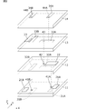
- FIG. 1 is a perspective view of a multilayer substrate 1 according to the first embodiment.
- FIG. 2 is a perspective view of the multilayer substrate 1 shown in FIG. 1 in a state before the layers are stacked.
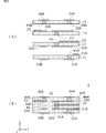
- FIG. 3A is a cross-sectional view of a plurality of base materials before the lamination press.
- FIG. 3B is a cross-sectional view after the lamination press, and is a cross-sectional view taken along the line AA in FIG.
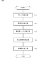
- FIG. 4 is a process flowchart showing the manufacturing procedure of the multilayer substrate 1.
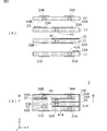
- 5A and 5B are cross-sectional views of the multilayer substrate 2 according to the second embodiment.
- FIG. 6 is a cross-sectional view taken along the line BB in FIG. 5 (B).
- FIG. 7 is a cross-sectional view of a multilayer substrate according to the third embodiment.
- FIG. 1 is a perspective view of a multilayer substrate 1 of the present embodiment.
- FIG. 2 is a perspective view of the multilayer substrate 1 shown in FIG. 1 in a state before the layers are stacked.
- FIG. 3A is a cross-sectional view of a plurality of base materials before the lamination press.
- FIG. 3B is a cross-sectional view after the lamination press, and is a cross-sectional view taken along the line AA in FIG.
- the multilayer substrate 1 has a rectangular flat plate-like appearance, and is formed by laminating a plurality of insulating base materials 11, 12, 13, and 14.
- These base materials 11, 12, 13, and 14 are thermoplastic resins such as liquid crystal polymer (LCP), and the laminate 100 is configured by stacking the base materials 11, 12, 13, and 14.
- LCP liquid crystal polymer
- Conductor patterns 31A and 31B are formed on the lower surface of the base material 11, and conductor patterns 32A and 32B are formed on the lower surface of the base material 12.
- Conductor patterns 33A and 33B are formed on the upper surface of the substrate 13, and conductor patterns 34A and 34B are formed on the upper surface of the substrate 14. These conductor patterns are obtained by patterning copper foil.
- interlayer connection conductors 41A and 41B are formed on the base material 11, and an interlayer connection conductor 42 is formed on the base material 12.
- An interlayer connection conductor 43 is formed on the base material 13, and interlayer connection conductors 44 ⁇ / b> A and 44 ⁇ / b> B are formed on the base material 14.
- the base material 12 corresponds to the “second base material” in the present invention.
- the substrate 12 corresponds to the “first substrate” in the present invention.
- the base material 14 corresponds to the “second base material” in the present invention.
- the interlayer connection conductor in the state shown in FIG. 3A is obtained by forming a hole in a base material and printing and applying, for example, a Sn-based conductive paste in the hole.
- the base material 11 is formed with gas venting portions 21A and 21B
- the base material 12 is formed with a gas venting portion 22
- the base material 13 is formed with a gas venting portion 23.
- the degassing portions 21A and 21B are disposed at positions close to the interlayer connection conductors 41A and 41B, the degassing portions 22 are disposed at positions close to the interlayer connection conductor 42, and the degassing portion 23 is disposed between the interlayer connection conductors 41A and 41B. It arrange
- the gas venting portions 21A, 21B, 22, and 23 are gas permeable sheets such as polyimide (PI).
- the thickness of these gas vent portions 21A, 21B, 22, and 23 is thinner than the thickness of the base materials 11, 12, 13, and 14, and is about the same as the conductor pattern. In this embodiment, it is set to 10 ⁇ m or more and 100 ⁇ m or less. If the thickness of the gas vents 21A, 21B, 22, 23 is less than 10 ⁇ m, the gas permeation performance may not be sufficient. When the thickness of the degassing portions 21A, 21B, 22, 23 exceeds 100 ⁇ m, the thickness of the multilayer substrate 1 may be too large.
- FIG. 4 is a process flowchart showing a manufacturing procedure of the multilayer substrate 1.
- the multilayer substrate 1 is manufactured by processing in the order of a pattern formation step S1, a through-hole formation step S2, a conductive paste filling step S3, a gas vent formation step S4, and a laminate formation step S5. .
- a predetermined conductor pattern is formed by photolithography on a liquid crystal polymer sheet covered with copper foil.
- through hole forming step S ⁇ b> 2 through holes are formed at positions where the interlayer connection conductors of the base materials 11, 12, 13 and 14 are formed.
- the conductive paste filling step S3 the conductive paste is filled into each through hole by a printing method.
- the degassing portion forming step S4 a polyimide sheet that becomes the degassing portions 21A, 21B, 22, 23 is pasted.
- the laminated body forming step S5 the base materials 11, 12, 13, and 14 are laminated and heated and pressed at a predetermined temperature (for example, 300 ° C.) within a range of 280 ° C.
- a multilayer substrate 1 as shown in FIGS. 1 and 3B is obtained.
- the conductive paste is melted and then solidified to form an interlayer connection conductor.
- FIG. 4 shows an example in which the venting portion is formed after the interlayer connection conductor is formed.
- both the step of forming the interlayer connection conductor and the step of forming the gas venting portion are before the layered body formation step.
- the order of the step of forming the interlayer connection conductor and the step of forming the gas vent is not limited to this.
- the size of the planar shape of the gas vents 21A, 21B, 22, and 23 is smaller than the base material 11, 12, 13, and 14. That is, it is included in the laminate 100. Thereby, the degassing portions 21A, 21B, 22, and 23 are not exposed to the end face of the laminated body 100, and the end face of the laminated body 100 is only an insulating base material, so that delamination of the base material is promoted. There is no.
- each degassing part is disposed in proximity to each interlayer connection conductor, so that the gas generated from each interlayer connection conductor during the above-described hot pressing is transmitted in the surface direction of the base material at the degassing part in the vicinity thereof. To do. Therefore, the gas generated from the interlayer connection conductor 41A effectively escapes from the interlayer connection conductor formation portion. For example, since the gas vent 21A is close to the interlayer connection conductor 41A, the gas generated from the interlayer connection conductor 41A permeates in the surface direction of the base material through the gas vent 21A. Therefore, the gas generated from the interlayer connection conductor 41A effectively escapes from the portion where the interlayer connection conductor 41 is formed.
- Liquid crystal polymer 0.6 g / m 2 ⁇ 24h
- Polyimide 63.7 g / m 2 ⁇ 24h
- the water vapor permeability of polyimide is 100 times or more compared with the water vapor permeability of the liquid crystal polymer. This tendency applies not only to water vapor but also to gas generated from conductive paste used for the interlayer connection conductor. Therefore, a polyimide sheet can be used effectively as a degassing part.
- FIG. 5A and 5B are cross-sectional views of the multilayer substrate 2 according to the second embodiment.
- FIG. 5A is a cross-sectional view of a plurality of base materials before being stacked and pressed.
- FIG. 5B is a cross-sectional view after the lamination press. These drawings are cross-sectional views at positions corresponding to FIGS. 3A and 3B shown in the first embodiment.
- FIG. 6 is a cross-sectional view taken along line BB in FIG. 5 (B).
- a gas vent 20 is formed on the base 12.
- the gas vent 20 includes a proximity portion 20A that surrounds the interlayer connection conductors 42 and 43 in a plan view, and an extending portion 20S that extends in the X-axis direction from the proximity portion 20A toward the outer edge of the substrate 12.
- the proximity portion 20 ⁇ / b> A has an annular shape and is close to the joint surface where the interlayer connection conductor 42 and the interlayer connection conductor 43 are joined.
- the extending portion 20S has a strip shape extending from the proximity portion 20A toward the outer edge of the base material.
- the gas vent portion 20 since the proximity portion 20A of the gas vent portion 20 is close to the joint surface between the interlayer connection conductor 42 and the interlayer connection conductor 43, the gas is effectively taken in by the proximity portion 20A. Gas easily escapes in the surface direction of the base materials 12 and 13 through the extending portion 20S.
- FIG. 7 is a cross-sectional view of a multilayer substrate according to the third embodiment. This figure corresponds to FIG. 6 shown in the second embodiment.
- the gas vent part of the present embodiment includes a proximity part 20A surrounding the interlayer connection conductor 43 in plan view, and an extension part that extends from the proximity part 20A in four directions (in the X-axis direction and the Y-axis direction) toward the outer edge of the base material. 20S1, 20S2, 20S3, and 20S4.
- the proximity portion 20 ⁇ / b> A has an annular shape and is close to the interlayer connection conductor 43.
- the extending portions 20S1, 20S2, 20S3, and 20S4 have a strip shape extending from the proximity portion 20A in the four-side direction of the base material.
- a plurality of extending portions may be provided. Moreover, they may extend radially. This increases the degassing effect.
- a gas-permeable sheet is pasted on a base material.
- a gas-permeable paste may be printed on a base material after forming the laminate.
- the base materials 11, 12, 13, and 14 are liquid crystal polymers (LCP), and the gas vent portions 21A, 21B, 22, and 23 are polyimide (PI).
- the punched portion is made of the same base material as the base material on which it is formed, and can be made of a material with a reduced filler content compared to the base material.
- the degassing part can also use a prepreg sheet mainly composed of a thermosetting resin that starts curing at a temperature lower than the temperature at the time of hot pressing.
- a prepreg sheet mainly composed of a thermosetting resin that starts curing at a temperature lower than the temperature at the time of hot pressing.
- a glass epoxy sheet epoxy prepreg
- gas venting part may be arranged at a position in contact with the interlayer connection conductor.
- the multilayer substrate according to the present invention is not limited to a substrate on which electronic components are mounted, and may itself constitute a chip component.
- it can be applied to various electronic components such as an antenna, an actuator, and a sensor.
- the present invention can be modified as appropriate without departing from the spirit of the present invention.
Landscapes
- Engineering & Computer Science (AREA)
- Microelectronics & Electronic Packaging (AREA)
- Manufacturing & Machinery (AREA)
- Production Of Multi-Layered Print Wiring Board (AREA)
Abstract
多層基板(1)は、絶縁性の第1基材(12)と、第1基材(12)に形成された層間接続導体(42)と、第1基材(12)に接する絶縁性の第2基材(13)と、第2基材(13)に形成された層間接続導体(43)とを備える。第1基材(12)と第2基材(13)との間には、層間接続導体に接するかまたは近接するガス抜き部(22)が部分的に配されている。ガス抜き部(22)は、第1基材(12)および第2基材(13)よりもガス透過性に優れ、第1基材(12)および第2基材(13)よりも薄い絶縁性樹脂からなる。
Description
本発明は、絶縁性基材が積層されて形成された多層基板およびその製造方法に関する。
多層基板の製造時、基材の積層工程において、加熱時に、加熱後に層間接続導体となる部分からガスが放出されることがある。このガスが多層基板内に残留すると、信頼性が低下し、所定の電気的特性を得にくいといった問題がある。
特許文献1には、基材の積層工程において加熱後に層間接続導体となる部分から放出されるガスを、基材の積層方向に放出させるため、面積の大きなグランド導体パターンに微小な複数のガス抜き孔を設けることが記載されている。
特許文献1に記載の多層基板において、導体パターンを構成する金属材料はガス透過性を有しないので、加熱後に層間接続導体となる部分から放出されるガスは、導体パターンに形成された微小なガス抜き孔から積層方向にのみ放出される。積層方向には複数の絶縁基材が配されている。一般に、絶縁基材にはフィラーが含有されており、フィラーはガス透過性を有しないので、ガスは多層基板内に閉じ込められやすい。つまり、このような従来の多層基板は、積層工程において加熱時に上記ガスが依然として抜け難い。
そこで本発明の目的は、加熱後に層間接続導体となる部分から、加熱時に放出されるガスの残留を抑制して、所定の信頼性および電気的特性を得やすくした多層基板、およびその製造方法を提供することにある。
(1)本発明の多層基板は、
絶縁性の第1基材と、
前記第1基材に形成された層間接続導体と、
前記第1基材に接する絶縁性の第2基材と、
前記第1基材および前記第2基材よりもガス透過性に優れ、前記第1基材および前記第2基材よりも薄い絶縁性樹脂からなり、前記第1基材と前記第2基材との間に部分的に配され、前記層間接続導体に接するかまたは近接するガス抜き部と、を備え、
前記第1基材および前記第2基材を含む複数の基材が積層され熱圧着された、
ことを特徴とする。
絶縁性の第1基材と、
前記第1基材に形成された層間接続導体と、
前記第1基材に接する絶縁性の第2基材と、
前記第1基材および前記第2基材よりもガス透過性に優れ、前記第1基材および前記第2基材よりも薄い絶縁性樹脂からなり、前記第1基材と前記第2基材との間に部分的に配され、前記層間接続導体に接するかまたは近接するガス抜き部と、を備え、
前記第1基材および前記第2基材を含む複数の基材が積層され熱圧着された、
ことを特徴とする。
上記構成により、加熱後に層間接続導体となる部分から放出されるガスはガス抜き部を経由して、第1基材および第2基材の面方向に抜ける。したがって、本発明の多層基板は、加熱後に層間接続導体となる部分から放出されるガスが抜けやすい構造の多層基板となる。そのため、所定の電気的特性を有する多層基板が得やすい。
また、ガス抜き部は部分的に配され、異種材料界面があまり大きくならないので、基材同士の密着力が大きく低下することはない。
また、ガス抜き部の厚さは、第1基材および第2基材の厚さよりも薄いので、多層基板の厚みが抑えられ、低背化されたチップ部品が得られる。
(2)前記ガス抜き部は、複数箇所に配されることが好ましい。これにより、加熱後に層間接続導体となる部分から放出されるガスがより抜けやすくなる。
(3)前記ガス抜き部は、前記第1基材および前記第2基材を含む複数の基材の積層体に内包されていることが好ましい。これにより、ガス抜き部は第1基材および第2基材が含まれた積層体の端面に露出しておらず、積層体の端面は絶縁性の基材のみであるので、基材の層間剥離が助長されることはない。
(4)前記ガス抜き部は、平面視で前記層間接続導体を囲む近接部と、前記近接部から前記第1基材の外縁に向かって延伸する延伸部と、を含むことが好ましい。この構造により、近接部によって、加熱後に層間接続導体となる部分から放出されるガスが取り込まれるとともに、延伸部によって、多層基板の端面方向にガスが抜けやすくなる。
(5)前記延伸部は、前記近接部から互いに異なる方向に延伸する複数の延伸部で構成されていてもよい。これにより、加熱後に層間接続導体となる部分から放出されるガスが層間接続導体形成部から、より抜けやすくなる。
(6)前記第2基材に形成され、前記第1基材に形成された前記層間接続導体に接合する層間接続導体を備えていてもよい。この構造では、層間接続導体が積層方向に連続するので、その部分では加熱時に多量のガスが発生しやすいが、上記構成により、ガスが効果的に抜ける。
(7)前記ガス抜き部は、前記第1基材および前記第2基材と同じ母材からなり、前記第1基材および前記第2基材に比較してフィラーの含有量が少ないことが好ましい。これにより、第1基材と第2基材との密着力が保たれる。
(8)前記第1基材および前記第2基材は例えば液晶ポリマーを主成分とし、前記ガス抜き部は例えばポリイミドを主成分とする。これにより、第1基材および第2基材の高温耐熱性およびガス抜き部の高いガス透過性を備える多層基板が得られる。
(9)本発明の多層基板の製造方法は、
絶縁性の第1基材に貫通孔を形成し、当該貫通孔に導電性ペーストを充填する導電性ペースト充填工程と、
前記第1基材よりもガス透過性に優れた絶縁性樹脂からなるガス抜き部を、平面視で前記貫通孔に近接するように、前記第1基材または当該第1基材に重なる第2基材に形成する、ガス抜き部形成工程と、
前記第1基材を含む複数の基材を積層し熱圧着して積層体を形成する積層体形成工程と、を有する。
絶縁性の第1基材に貫通孔を形成し、当該貫通孔に導電性ペーストを充填する導電性ペースト充填工程と、
前記第1基材よりもガス透過性に優れた絶縁性樹脂からなるガス抜き部を、平面視で前記貫通孔に近接するように、前記第1基材または当該第1基材に重なる第2基材に形成する、ガス抜き部形成工程と、
前記第1基材を含む複数の基材を積層し熱圧着して積層体を形成する積層体形成工程と、を有する。
上記製造方法により、加熱後に層間接続導体となる部分から、加熱時に放出されるガスの残留が抑制される。
本発明によれば、加熱後に層間接続導体となる部分から、加熱時に放出されるガスの残留が抑制されて、所定の信頼性および電気的特性を有する多層基板が得られる。
《第1の実施形態》
図1は本実施形態の多層基板1の斜視図である。図2は、図1に示す多層基板1の、各層の積層前の状態での斜視図である。また、図3(A)は複数の基材の積層プレス前の段階での断面図である。図3(B)は積層プレス後の断面図であり、図1におけるA-A部分の断面図である。
図1は本実施形態の多層基板1の斜視図である。図2は、図1に示す多層基板1の、各層の積層前の状態での斜視図である。また、図3(A)は複数の基材の積層プレス前の段階での断面図である。図3(B)は積層プレス後の断面図であり、図1におけるA-A部分の断面図である。
多層基板1は矩形平板状の外観を有し、絶縁性の複数の基材11,12,13,14が積層されてなる。これら基材11,12,13,14は液晶ポリマー(LCP)等の熱可塑性樹脂であり、基材11,12,13,14の積層によって積層体100が構成されている。
基材11の下面には導体パターン31A,31Bが形成されていて、基材12の下面には導体パターン32A,32Bが形成されている。基材13の上面には導体パターン33A,33Bが形成されていて、基材14の上面には導体パターン34A,34Bが形成されている。これら導体パターンは銅箔をパターン化したものである。
また、基材11には層間接続導体41A,41Bが形成されていて、基材12には層間接続導体42が形成されている。基材13には層間接続導体43が形成されていて、基材14には層間接続導体44A,44Bが形成されている。
上記複数の基材のうち、例えば基材11を本発明における「第1基材」と見なすと、基材12は本発明における「第2基材」に相当する。また、基材12を本発明における「第1基材」と見なすと、基材13は本発明における「第2基材」に相当する。また、基材13を本発明における「第1基材」と見なすと、基材14は本発明における「第2基材」に相当する。
図3(A)に示す状態の層間接続導体は、基材に孔を形成し、その孔内に、例えばSn系導電性ペーストを印刷塗布したものである。
更に、基材11にはガス抜き部21A,21Bが形成されていて、基材12にはガス抜き部22が形成されていて、基材13にはガス抜き部23が形成されている。
上記ガス抜き部21A,21Bはそれぞれ層間接続導体41A,41Bに近接する位置に配置されていて、ガス抜き部22は層間接続導体42に近接する位置に配置されていて、ガス抜き部23は層間接続導体44Bに近接する位置に配置されている。
ガス抜き部21A,21B,22,23は、例えばポリイミド(PI)等の、ガス透過性を有するシートである。これらガス抜き部21A,21B,22,23の厚さは、基材11,12,13,14の厚さよりも薄く、上記導体パターンと同程度である。本実施形態では、10μm以上100μm以下に設定される。ガス抜き部21A,21B,22,23の厚さが10μm未満の場合、ガス透過性能が充分でない場合が考えられる。ガス抜き部21A,21B,22,23の厚さが100μm超の場合、多層基板1の厚さが大きくなり過ぎる場合が考えられる。
ここで、第1の実施形態の多層基板1の製造手順について説明する。図4は、多層基板1の製造手順を示す工程フローチャートである。この例では、多層基板1は、パターン形成工程S1、貫通孔形成工程S2、導電性ペースト充填工程S3、ガス抜き部形成工程S4、積層体形成工程S5、の順に処理されることで製造される。
パターン形成工程S1では、銅箔張りの液晶ポリマーシートに対してフォトリソグラフィによって所定の導体パターンを形成する。貫通孔形成工程S2では、基材11,12,13,14の層間接続導体形成位置にそれぞれ貫通孔を形成する。導電性ペースト充填工程S3では、印刷法によって、各貫通孔に導電性ペーストを充填する。ガス抜き部形成工程S4では、ガス抜き部21A,21B,22,23となるポリイミドシートを貼付する。積層体形成工程S5では、基材11,12,13,14を積層し、例えば280℃以上320℃以下の範囲内の所定の温度(例えば300℃)で加熱プレスする。このことによって、図1、図3(B)に示すような多層基板1を得る。この加熱プレス時に、上記導電性ペーストを溶融させ、その後に固化させて層間接続導体を形成する。
図4では、層間接続導体を形成した後にガス抜き部を形成する例を示したが、層間接続導体を形成する工程とガス抜き部を形成する工程は、いずれも積層体形成工程の前であればよく、層間接続導体を形成する工程とガス抜き部を形成する工程の順序はこれに限らない。
図2、図3(A)に示すように、ガス抜き部21A,21B,22,23の平面形状のサイズは、基材11,12,13,14よりも小さい。すなわち、積層体100に内包されている。これにより、ガス抜き部21A,21B,22,23は積層体100の端面に露出せず、積層体100の端面は絶縁性の基材のみであるので、基材の層間剥離が助長されることはない。
上述のとおり、各ガス抜き部は各層間接続導体に近接配置されているので、上記加熱プレス時に各層間接続導体から発生されるガスは、その近傍のガス抜き部で基材の面方向に透過する。そのため、層間接続導体41Aから発生されるガスは層間接続導体形成部から効果的に抜ける。例えば、層間接続導体41Aにガス抜き部21Aが近接しているので、層間接続導体41Aから発生されるガスはガス抜き部21Aで基材の面方向に透過する。そのため、層間接続導体41Aから発生されるガスは層間接続導体41の形成部から効果的に抜ける。
ここで、液晶ポリマーとポリイミドのガス透過性の差異について示す。JIS Z0208に規定される透湿度試験方法によって水蒸気透過度を測定したところ、測定結果は次のとおりであった。
液晶ポリマー:0.6 g/m2・24h
ポリイミド:63.7 g/m2・24h
このように、ポリイミドの水蒸気透過度は、液晶ポリマーの水蒸気透過度に比べて、100倍以上である。この傾向は水蒸気に限らず、層間接続導体に用いられる導電性ペーストから発生されるガスにも当てはまる。よって、ポリイミドのシートをガス抜き部として有効に用いることができる。
ポリイミド:63.7 g/m2・24h
このように、ポリイミドの水蒸気透過度は、液晶ポリマーの水蒸気透過度に比べて、100倍以上である。この傾向は水蒸気に限らず、層間接続導体に用いられる導電性ペーストから発生されるガスにも当てはまる。よって、ポリイミドのシートをガス抜き部として有効に用いることができる。
《第2の実施形態》
図5(A)、図5(B)は第2の実施形態に係る多層基板2の断面図である。図5(A)は複数の基材の積層プレス前の段階での断面図である。図5(B)は積層プレス後の断面図である。これらの図は第1の実施形態で示した図3(A)、図3(B)にそれぞれ対応する位置での断面図である。また、図6は図5(B)におけるB-B部分での横断面図である。基材12にはガス抜き部20が形成されている。このガス抜き部20は、平面視で層間接続導体42,43を囲む近接部20Aと、近接部20Aから基材12の外縁に向かってX軸方向へ延伸する延伸部20Sと、を含む。
図5(A)、図5(B)は第2の実施形態に係る多層基板2の断面図である。図5(A)は複数の基材の積層プレス前の段階での断面図である。図5(B)は積層プレス後の断面図である。これらの図は第1の実施形態で示した図3(A)、図3(B)にそれぞれ対応する位置での断面図である。また、図6は図5(B)におけるB-B部分での横断面図である。基材12にはガス抜き部20が形成されている。このガス抜き部20は、平面視で層間接続導体42,43を囲む近接部20Aと、近接部20Aから基材12の外縁に向かってX軸方向へ延伸する延伸部20Sと、を含む。
近接部20Aは円環状であり、層間接続導体42と層間接続導体43とが接合する接合面に近接している。延伸部20Sは、近接部20Aから基材の外縁方向へ延びる帯状である。
層間接続導体が積層方向に連続する部分では、積層体の加熱プレス時に多量のガスが発生しやすい。本実施形態によれば、層間接続導体42と層間接続導体43との接合面にガス抜き部20の近接部20Aが近接しているため、この近接部20Aでガスが効果的に取り込まれ、そのガスが延伸部20Sを経由して基材12,13の面方向に抜けやすい。
その他の構成は第1の実施形態で示したものと同様である。
《第3の実施形態》
図7は第3の実施形態に係る多層基板の横断面図である。この図は第2の実施形態で示した図6に対応する図である。
図7は第3の実施形態に係る多層基板の横断面図である。この図は第2の実施形態で示した図6に対応する図である。
本実施形態のガス抜き部は、平面視で層間接続導体43を囲む近接部20Aと、近接部20Aから基材の外縁に向かって四方に(X軸方向およびY軸方向に)延伸する延伸部20S1,20S2,20S3,20S4と、を含む。
近接部20Aは円環状であり、層間接続導体43に近接している。延伸部20S1,20S2,20S3,20S4は、近接部20Aから基材の四辺方向へ延びる帯状である。
本実施形態のように、延伸部は複数であってもよい。またそれらが放射状に延伸していてもよい。このことによって、ガス抜き効果が高まる。
《他の実施形態》
以上の各実施形態では、一単位の部品について図示したが、当然ながら、複数の素子形成部を含む集合基板状態で各工程の処理がなされ(大判プロセスによって製造され)、最後に個片に分離されてもよい。
以上の各実施形態では、一単位の部品について図示したが、当然ながら、複数の素子形成部を含む集合基板状態で各工程の処理がなされ(大判プロセスによって製造され)、最後に個片に分離されてもよい。
以上の各実施形態では、ガス透過性を有するシートを基材に貼付する例を示したが、積層体形成後にガス透過性を有するペーストを基材に印刷形成してもよい。
以上の各実施形態では、基材11,12,13,14は、液晶ポリマー(LCP)であり、ガス抜き部21A,21B,22,23はポリイミド(PI)である例を示したが、ガス抜き部は、それが形成される基材と同じ母材からなり、基材と比較してフィラーの含有量を少なくした材料とすることが可能である。
また、ガス抜き部は、加熱プレス時の温度よりも低い温度で硬化を開始する熱硬化性樹脂を主成分とするプリプレグシートを用いることもできる。例えば、ガラスエポキシシート(エポキシプリプレグ)を用いることができる。
また、ガス抜き部は層間接続導体に接する位置に配置されていてもよい。
本発明に係る多層基板は、電子部品が実装される基板であることに限らず、それ自体がチップ部品を構成してもよい。例えば、アンテナ、アクチュエータ、センサ等各種電子部品に適用できる。このように、本発明は、その趣旨を逸脱しない範囲で適宜変更が可能である。
最後に、上述の実施形態の説明は、すべての点で例示であって、制限的なものではない。当業者にとって変形および変更が適宜可能である。例えば、異なる実施形態で示した構成の部分的な置換または組み合わせが可能である。本発明の範囲は、上述の実施形態ではなく、特許請求の範囲によって示される。さらに、本発明の範囲には、特許請求の範囲と均等の意味および範囲内でのすべての変更が含まれることが意図される。
1,2…多層基板
11,12,13,14…基材
20A…近接部
20S…延伸部
20S1,20S2,20S3,20S4…延伸部
21A,21B,22,23…ガス抜き部
31A,31B…導体パターン
32A,32B…導体パターン
33A,33B…導体パターン
34A,34B…導体パターン
41A,41B…層間接続導体
42,43…層間接続導体
44A,44B…層間接続導体
100…積層体
11,12,13,14…基材
20A…近接部
20S…延伸部
20S1,20S2,20S3,20S4…延伸部
21A,21B,22,23…ガス抜き部
31A,31B…導体パターン
32A,32B…導体パターン
33A,33B…導体パターン
34A,34B…導体パターン
41A,41B…層間接続導体
42,43…層間接続導体
44A,44B…層間接続導体
100…積層体
Claims (9)
- 絶縁性の第1基材と、
前記第1基材に形成された層間接続導体と、
前記第1基材に接する絶縁性の第2基材と、
前記第1基材および前記第2基材よりもガス透過性に優れ、前記第1基材および前記第2基材よりも薄い絶縁性樹脂からなり、前記第1基材と前記第2基材との間に部分的に配され、前記層間接続導体に接するかまたは近接するガス抜き部と、を備え、
前記第1基材および前記第2基材を含む複数の基材が積層され熱圧着された、
多層基板。 - 前記ガス抜き部は、複数箇所に配される、請求項1に記載の多層基板。
- 前記ガス抜き部は、前記第1基材および前記第2基材を含む複数の基材の積層体に内包されている、請求項1または2に記載の多層基板。
- 前記ガス抜き部は、平面視で前記層間接続導体を囲む近接部と、前記近接部から前記第1基材の外縁に向かって延伸する延伸部と、を含む、請求項1から3のいずれかに記載の多層基板。
- 前記延伸部は、前記近接部から互いに異なる方向に延伸する複数の延伸部で構成される、請求項4に記載の多層基板。
- 前記第2基材に形成され、前記第1基材に形成された前記層間接続導体に接合する層間接続導体を備える、請求項1から5のいずれかに記載の多層基板。
- 前記ガス抜き部は、前記第1基材および前記第2基材と同じ母材からなり、前記第1基材および前記第2基材に比較してフィラーの含有量が少ない、請求項1から6のいずれかに記載の多層基板。
- 前記第1基材および前記第2基材は液晶ポリマーを主成分とし、前記ガス抜き部はポリイミドを主成分とする、請求項1から6のいずれかに記載の多層基板。
- 絶縁性の第1基材に貫通孔を形成し、当該貫通孔に導電性ペーストを充填する導電性ペースト充填工程と、
前記第1基材よりもガス透過性に優れた絶縁性樹脂からなるガス抜き部を、平面視で前記貫通孔に近接するように、前記第1基材または当該第1基材に重なる第2基材に形成する、ガス抜き部形成工程と、
前記第1基材を含む複数の基材を積層し熱圧着して積層体を形成する積層体形成工程と、を有する、
多層基板の製造方法。
Priority Applications (1)
| Application Number | Priority Date | Filing Date | Title |
|---|---|---|---|
| CN201790001033.5U CN209676640U (zh) | 2016-10-27 | 2017-10-23 | 多层基板 |
Applications Claiming Priority (2)
| Application Number | Priority Date | Filing Date | Title |
|---|---|---|---|
| JP2016210940 | 2016-10-27 | ||
| JP2016-210940 | 2016-10-27 |
Publications (1)
| Publication Number | Publication Date |
|---|---|
| WO2018079477A1 true WO2018079477A1 (ja) | 2018-05-03 |
Family
ID=62024964
Family Applications (1)
| Application Number | Title | Priority Date | Filing Date |
|---|---|---|---|
| PCT/JP2017/038165 Ceased WO2018079477A1 (ja) | 2016-10-27 | 2017-10-23 | 多層基板およびその製造方法 |
Country Status (2)
| Country | Link |
|---|---|
| CN (1) | CN209676640U (ja) |
| WO (1) | WO2018079477A1 (ja) |
Cited By (1)
| Publication number | Priority date | Publication date | Assignee | Title |
|---|---|---|---|---|
| JP2020120024A (ja) * | 2019-01-25 | 2020-08-06 | 株式会社村田製作所 | 多層基板の製造方法 |
Citations (3)
| Publication number | Priority date | Publication date | Assignee | Title |
|---|---|---|---|---|
| JPH08264941A (ja) * | 1995-03-24 | 1996-10-11 | Ibiden Co Ltd | ビルドアップ多層プリント配線板及びその製造方法 |
| JP2003031949A (ja) * | 2001-07-12 | 2003-01-31 | Sumitomo Metal Mining Co Ltd | 多層基板、多層基板の製造方法および接着用構造体 |
| JP2005136347A (ja) * | 2003-10-31 | 2005-05-26 | Denso Corp | 多層基板及びその製造方法 |
-
2017
- 2017-10-23 WO PCT/JP2017/038165 patent/WO2018079477A1/ja not_active Ceased
- 2017-10-23 CN CN201790001033.5U patent/CN209676640U/zh active Active
Patent Citations (3)
| Publication number | Priority date | Publication date | Assignee | Title |
|---|---|---|---|---|
| JPH08264941A (ja) * | 1995-03-24 | 1996-10-11 | Ibiden Co Ltd | ビルドアップ多層プリント配線板及びその製造方法 |
| JP2003031949A (ja) * | 2001-07-12 | 2003-01-31 | Sumitomo Metal Mining Co Ltd | 多層基板、多層基板の製造方法および接着用構造体 |
| JP2005136347A (ja) * | 2003-10-31 | 2005-05-26 | Denso Corp | 多層基板及びその製造方法 |
Cited By (2)
| Publication number | Priority date | Publication date | Assignee | Title |
|---|---|---|---|---|
| JP2020120024A (ja) * | 2019-01-25 | 2020-08-06 | 株式会社村田製作所 | 多層基板の製造方法 |
| JP7234651B2 (ja) | 2019-01-25 | 2023-03-08 | 株式会社村田製作所 | 多層基板の製造方法 |
Also Published As
| Publication number | Publication date |
|---|---|
| CN209676640U (zh) | 2019-11-22 |
Similar Documents
| Publication | Publication Date | Title |
|---|---|---|
| JP3407737B2 (ja) | 多層基板の製造方法およびその製造方法によって形成される多層基板 | |
| JP5151265B2 (ja) | 多層配線基板及び多層配線基板の製造方法 | |
| JP5895635B2 (ja) | 配線板の製造方法、配線板およびビアの構造 | |
| JP2013211519A (ja) | 多層配線基板の製造方法 | |
| JP2013211518A (ja) | 多層配線基板およびその製造方法 | |
| JP5481675B2 (ja) | 基板内蔵用チップ抵抗器およびその製造方法 | |
| JP2026012559A (ja) | プリント配線板及びプリント配線板の製造方法 | |
| JP6497486B2 (ja) | 多層基板およびその製造方法 | |
| JP5663804B2 (ja) | 基板内蔵用チップ抵抗器およびその製造方法 | |
| WO2018079477A1 (ja) | 多層基板およびその製造方法 | |
| JP2009152496A (ja) | プリント配線板の製造方法 | |
| JP2013135032A (ja) | マスクフィルムおよびそれを用いた回路基板の製造方法 | |
| JP4417938B2 (ja) | プリント配線基板の製造方法 | |
| JP5585035B2 (ja) | 回路基板の製造方法 | |
| JP2015170615A (ja) | 多層基板および多層基板の製造方法 | |
| JP2006324574A (ja) | 多層プリント配線基板とその製造方法 | |
| CN219644174U (zh) | 多层基板 | |
| JP5633256B2 (ja) | 部品内蔵基板の製造方法 | |
| JP4821276B2 (ja) | 多層プリント配線板の製造方法及び多層プリント配線板 | |
| JP4978709B2 (ja) | 電子部品内蔵配線基板 | |
| JP2009099600A (ja) | 受動素子シート、これを実装した回路配線基板及びその製造方法 | |
| JP4754357B2 (ja) | 多層基板の製造方法及び多層基板の製造装置 | |
| JP6001475B2 (ja) | 配線基板 | |
| JP5761405B2 (ja) | 電子部品内蔵配線基板 | |
| JP2012109615A (ja) | 電子部品内蔵配線基板 |
Legal Events
| Date | Code | Title | Description |
|---|---|---|---|
| 121 | Ep: the epo has been informed by wipo that ep was designated in this application |
Ref document number: 17863663 Country of ref document: EP Kind code of ref document: A1 |
|
| NENP | Non-entry into the national phase |
Ref country code: DE |
|
| 122 | Ep: pct application non-entry in european phase |
Ref document number: 17863663 Country of ref document: EP Kind code of ref document: A1 |
|
| NENP | Non-entry into the national phase |
Ref country code: JP |