WO2018078487A1 - 情報処理装置、表示装置および電子機器 - Google Patents
情報処理装置、表示装置および電子機器 Download PDFInfo
- Publication number
- WO2018078487A1 WO2018078487A1 PCT/IB2017/056459 IB2017056459W WO2018078487A1 WO 2018078487 A1 WO2018078487 A1 WO 2018078487A1 IB 2017056459 W IB2017056459 W IB 2017056459W WO 2018078487 A1 WO2018078487 A1 WO 2018078487A1
- Authority
- WO
- WIPO (PCT)
- Prior art keywords
- film
- substrate
- layer
- housing
- information processing
- Prior art date
- Legal status (The legal status is an assumption and is not a legal conclusion. Google has not performed a legal analysis and makes no representation as to the accuracy of the status listed.)
- Ceased
Links
Images






Classifications
-
- H—ELECTRICITY
- H10—SEMICONDUCTOR DEVICES; ELECTRIC SOLID-STATE DEVICES NOT OTHERWISE PROVIDED FOR
- H10K—ORGANIC ELECTRIC SOLID-STATE DEVICES
- H10K59/00—Integrated devices, or assemblies of multiple devices, comprising at least one organic light-emitting element covered by group H10K50/00
- H10K59/10—OLED displays
-
- G—PHYSICS
- G09—EDUCATION; CRYPTOGRAPHY; DISPLAY; ADVERTISING; SEALS
- G09F—DISPLAYING; ADVERTISING; SIGNS; LABELS OR NAME-PLATES; SEALS
- G09F9/00—Indicating arrangements for variable information in which the information is built-up on a support by selection or combination of individual elements
- G09F9/30—Indicating arrangements for variable information in which the information is built-up on a support by selection or combination of individual elements in which the desired character or characters are formed by combining individual elements
- G09F9/301—Indicating arrangements for variable information in which the information is built-up on a support by selection or combination of individual elements in which the desired character or characters are formed by combining individual elements flexible foldable or roll-able electronic displays, e.g. thin LCD, OLED
-
- G—PHYSICS
- G06—COMPUTING OR CALCULATING; COUNTING
- G06F—ELECTRIC DIGITAL DATA PROCESSING
- G06F1/00—Details not covered by groups G06F3/00 - G06F13/00 and G06F21/00
- G06F1/16—Constructional details or arrangements
- G06F1/1601—Constructional details related to the housing of computer displays, e.g. of CRT monitors, of flat displays
-
- G—PHYSICS
- G06—COMPUTING OR CALCULATING; COUNTING
- G06F—ELECTRIC DIGITAL DATA PROCESSING
- G06F1/00—Details not covered by groups G06F3/00 - G06F13/00 and G06F21/00
- G06F1/16—Constructional details or arrangements
- G06F1/1613—Constructional details or arrangements for portable computers
- G06F1/1626—Constructional details or arrangements for portable computers with a single-body enclosure integrating a flat display, e.g. Personal Digital Assistants [PDAs]
-
- G—PHYSICS
- G06—COMPUTING OR CALCULATING; COUNTING
- G06F—ELECTRIC DIGITAL DATA PROCESSING
- G06F1/00—Details not covered by groups G06F3/00 - G06F13/00 and G06F21/00
- G06F1/16—Constructional details or arrangements
- G06F1/1613—Constructional details or arrangements for portable computers
- G06F1/1633—Constructional details or arrangements of portable computers not specific to the type of enclosures covered by groups G06F1/1615 - G06F1/1626
- G06F1/1637—Details related to the display arrangement, including those related to the mounting of the display in the housing
- G06F1/1643—Details related to the display arrangement, including those related to the mounting of the display in the housing the display being associated to a digitizer, e.g. laptops that can be used as penpads
-
- G—PHYSICS
- G06—COMPUTING OR CALCULATING; COUNTING
- G06F—ELECTRIC DIGITAL DATA PROCESSING
- G06F1/00—Details not covered by groups G06F3/00 - G06F13/00 and G06F21/00
- G06F1/16—Constructional details or arrangements
- G06F1/1613—Constructional details or arrangements for portable computers
- G06F1/1633—Constructional details or arrangements of portable computers not specific to the type of enclosures covered by groups G06F1/1615 - G06F1/1626
- G06F1/1637—Details related to the display arrangement, including those related to the mounting of the display in the housing
- G06F1/1652—Details related to the display arrangement, including those related to the mounting of the display in the housing the display being flexible, e.g. mimicking a sheet of paper, or rollable
-
- G—PHYSICS
- G06—COMPUTING OR CALCULATING; COUNTING
- G06F—ELECTRIC DIGITAL DATA PROCESSING
- G06F1/00—Details not covered by groups G06F3/00 - G06F13/00 and G06F21/00
- G06F1/16—Constructional details or arrangements
- G06F1/1613—Constructional details or arrangements for portable computers
- G06F1/1633—Constructional details or arrangements of portable computers not specific to the type of enclosures covered by groups G06F1/1615 - G06F1/1626
- G06F1/1675—Miscellaneous details related to the relative movement between the different enclosures or enclosure parts
- G06F1/1681—Details related solely to hinges
-
- G—PHYSICS
- G06—COMPUTING OR CALCULATING; COUNTING
- G06F—ELECTRIC DIGITAL DATA PROCESSING
- G06F1/00—Details not covered by groups G06F3/00 - G06F13/00 and G06F21/00
- G06F1/16—Constructional details or arrangements
- G06F1/1613—Constructional details or arrangements for portable computers
- G06F1/1633—Constructional details or arrangements of portable computers not specific to the type of enclosures covered by groups G06F1/1615 - G06F1/1626
- G06F1/1675—Miscellaneous details related to the relative movement between the different enclosures or enclosure parts
- G06F1/1683—Miscellaneous details related to the relative movement between the different enclosures or enclosure parts for the transmission of signal or power between the different housings, e.g. details of wired or wireless communication, passage of cabling
-
- G—PHYSICS
- G06—COMPUTING OR CALCULATING; COUNTING
- G06F—ELECTRIC DIGITAL DATA PROCESSING
- G06F3/00—Input arrangements for transferring data to be processed into a form capable of being handled by the computer; Output arrangements for transferring data from processing unit to output unit, e.g. interface arrangements
- G06F3/01—Input arrangements or combined input and output arrangements for interaction between user and computer
- G06F3/03—Arrangements for converting the position or the displacement of a member into a coded form
- G06F3/041—Digitisers, e.g. for touch screens or touch pads, characterised by the transducing means
-
- G—PHYSICS
- G06—COMPUTING OR CALCULATING; COUNTING
- G06F—ELECTRIC DIGITAL DATA PROCESSING
- G06F3/00—Input arrangements for transferring data to be processed into a form capable of being handled by the computer; Output arrangements for transferring data from processing unit to output unit, e.g. interface arrangements
- G06F3/01—Input arrangements or combined input and output arrangements for interaction between user and computer
- G06F3/03—Arrangements for converting the position or the displacement of a member into a coded form
- G06F3/041—Digitisers, e.g. for touch screens or touch pads, characterised by the transducing means
- G06F3/0412—Digitisers structurally integrated in a display
-
- G—PHYSICS
- G06—COMPUTING OR CALCULATING; COUNTING
- G06F—ELECTRIC DIGITAL DATA PROCESSING
- G06F3/00—Input arrangements for transferring data to be processed into a form capable of being handled by the computer; Output arrangements for transferring data from processing unit to output unit, e.g. interface arrangements
- G06F3/01—Input arrangements or combined input and output arrangements for interaction between user and computer
- G06F3/03—Arrangements for converting the position or the displacement of a member into a coded form
- G06F3/041—Digitisers, e.g. for touch screens or touch pads, characterised by the transducing means
- G06F3/044—Digitisers, e.g. for touch screens or touch pads, characterised by the transducing means by capacitive means
-
- G—PHYSICS
- G06—COMPUTING OR CALCULATING; COUNTING
- G06F—ELECTRIC DIGITAL DATA PROCESSING
- G06F3/00—Input arrangements for transferring data to be processed into a form capable of being handled by the computer; Output arrangements for transferring data from processing unit to output unit, e.g. interface arrangements
- G06F3/01—Input arrangements or combined input and output arrangements for interaction between user and computer
- G06F3/03—Arrangements for converting the position or the displacement of a member into a coded form
- G06F3/041—Digitisers, e.g. for touch screens or touch pads, characterised by the transducing means
- G06F3/044—Digitisers, e.g. for touch screens or touch pads, characterised by the transducing means by capacitive means
- G06F3/0448—Details of the electrode shape, e.g. for enhancing the detection of touches, for generating specific electric field shapes, for enhancing display quality
-
- H—ELECTRICITY
- H05—ELECTRIC TECHNIQUES NOT OTHERWISE PROVIDED FOR
- H05B—ELECTRIC HEATING; ELECTRIC LIGHT SOURCES NOT OTHERWISE PROVIDED FOR; CIRCUIT ARRANGEMENTS FOR ELECTRIC LIGHT SOURCES, IN GENERAL
- H05B33/00—Electroluminescent light sources
- H05B33/02—Details
-
- H—ELECTRICITY
- H10—SEMICONDUCTOR DEVICES; ELECTRIC SOLID-STATE DEVICES NOT OTHERWISE PROVIDED FOR
- H10K—ORGANIC ELECTRIC SOLID-STATE DEVICES
- H10K50/00—Organic light-emitting devices
-
- G—PHYSICS
- G06—COMPUTING OR CALCULATING; COUNTING
- G06F—ELECTRIC DIGITAL DATA PROCESSING
- G06F2203/00—Indexing scheme relating to G06F3/00 - G06F3/048
- G06F2203/041—Indexing scheme relating to G06F3/041 - G06F3/045
- G06F2203/04102—Flexible digitiser, i.e. constructional details for allowing the whole digitising part of a device to be flexed or rolled like a sheet of paper
-
- G—PHYSICS
- G06—COMPUTING OR CALCULATING; COUNTING
- G06F—ELECTRIC DIGITAL DATA PROCESSING
- G06F2203/00—Indexing scheme relating to G06F3/00 - G06F3/048
- G06F2203/041—Indexing scheme relating to G06F3/041 - G06F3/045
- G06F2203/04103—Manufacturing, i.e. details related to manufacturing processes specially suited for touch sensitive devices
Definitions
- the second housing includes an end portion parallel to the rotation axis, and the first film and the panel substrate slide in the second slit, One film is away from the end, and the panel substrate is away from the end.
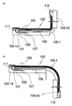
- the foldable touch panel includes the panel substrate 101, the first film 102, the second film 103, the first housing 104-1, the second housing 104-2, and the hinge 105-. 1.
- a circuit board 106 and a flexible board FPC 107 are included.
- the panel substrate 101, the first film 102, and the second film 103 are all flexible.
- the first housing 104-1 can be rotated with respect to the second housing 104-2 around the rotation axis of the hinge 105-1.
- the state shown in FIG. 1A can be said to be a state in which the information processing apparatus is bent around the rotation axis of the hinge 105-1.
- a touch panel 300 illustrated in FIG. 3A includes a scan line driver circuit 303g (1) and an image signal line driver circuit 303s (1).
- the scan line driver circuit 303g (1) can supply a selection signal to the pixel 302.
- the image signal line driver circuit 303s (1) can supply an image signal to the pixel 302.
- the touch panel 400 illustrated in FIG. 3B includes a scan line driver circuit and an image signal line driver circuit.
- the scan line driver circuit can supply a selection signal to the pixel 302.
- the image signal line driver circuit can supply an image signal to the pixel 302.
- the touch panel 400 includes a region 401 (1) and a region 401 (2) in which the socket 109 is disposed, and a drive circuit is provided for each using the COG method.
- a signal for reading a recorded imaging signal, a signal for initializing the imaging pixel circuit, a signal for determining the time for which the imaging pixel circuit detects light, and the like are selected as control signals by selecting a predetermined imaging pixel circuit. it can.
- the touch panel 300 can be folded in an area indicated by a line segment 406.
- the touch panel 300 can be folded between a region where the scanning line driver circuit 303g (1) and the image signal line driver circuit 303s (1) are arranged and a region where the display portion is arranged.
- the touch panel 400 can be folded between the region where the region 401 (1) and the region 401 (2) are arranged and the region where the display unit is arranged. Thereby, the area of the 2nd part 104-1B can be made small.
- the area of the touch panel 300 where the scanning line driver circuit 303g (1) and the image signal line driver circuit 303s (1) are arranged can be larger than the area of the second portion 104-1B.
- the area of the touch panel 400 in which the region 401 (1) and the region 401 (2) are arranged can be larger than the area of the second portion 104-1B.
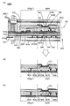
- the first light-emitting element 350R includes a first lower electrode 351R, an upper electrode 352, and a layer 353 containing a light-emitting organic compound between the first lower electrode 351R and the upper electrode 352 (see FIG. 5C). ).
- the first colored layer 367R is positioned so as to overlap with the first light-emitting element 350R. Accordingly, part of light emitted from the first light-emitting element 350R passes through the sealing material 360 that also functions as an optically bonding layer and the first colored layer 367R, and is indicated by an arrow in the drawing. Thus, the light is emitted to the outside of the light emitting module 380R.
- the information processing device of one embodiment of the present invention includes the first film 102 in the direction of the arrow.
- the touch panel 300 includes an insulating film 321.
- the insulating film 321 covers the transistor 302t.
- the insulating film 321 can be used as a layer for planarizing unevenness caused by the pixel circuit.
- an insulating film in which a layer capable of suppressing diffusion of impurities into the transistor 302t and the like is stacked can be applied to the insulating film 321.
- the image signal line driver circuit 303s (1) includes a transistor 303t and a capacitor 303c. Note that the driver circuit can be formed over the same substrate in the same process as the pixel circuit.
- a capacitive touch sensor can be applied.
- the electrostatic capacity method include a surface electrostatic capacity method and a projection electrostatic capacity method.
- the projected capacitive touch sensor 595 includes an electrode 591 and an electrode 592.
- the electrode 591 is electrically connected to any one of the plurality of wirings 598
- the electrode 592 is electrically connected to any one of the plurality of wirings 598.
- the electrode 591 has a quadrangular shape, and is repeatedly arranged in a direction intersecting with the direction in which the electrode 592 extends.
- the sub-pixel 502R includes a pixel circuit including a first light-emitting element 550R and a transistor 502t that can supply power to the first light-emitting element 550R.
- the light emitting module 580R includes a first light emitting element 550R and an optical element (for example, the first colored layer 567R).
- the sealing material 560 is provided on the light extraction side, the sealing material 560 is in contact with the first light-emitting element 550R and the first colored layer 567R.
- the display portion 501 includes wiring such as scanning lines, signal lines, and power supply lines. Various conductive films can be used for the wiring.
- FIGS. 1-10 A structure in the case of applying a bottom-gate transistor to the display portion 501 is illustrated in FIGS.
- the display portion 501 includes a light shielding layer 567BM in a direction in which light is emitted.
- the light-blocking layer 567BM is provided so as to surround the colored layer (for example, the first colored layer 567R).
- the display unit 501 includes an insulating film 521.
- the insulating film 521 covers the transistor 502t.
- the insulating film 521 can be used as a layer for planarizing unevenness caused by the pixel circuit.
- a stacked film including a layer that can suppress diffusion of impurities can be applied to the insulating film 521.
- a reduction in reliability of the transistor 502t or the like due to impurities diffused from the first colored layer 567R can be suppressed.
- the panel substrate of one embodiment of the present invention is preferably a touch panel.
- the display unit of the touch panel includes a touch sensor, and a touch position is detected by touching the first film 102 with a thin member such as a pen or a pencil or a finger. That is, the panel substrate 101 is protected by the first film 102.
- the element formation region 603 Since the element formation region 603 has a thickness, the element formation region 603 cannot be formed only on the neutral surface 605. However, if the element formation region 603 is formed near the neutral surface 605, bending stress generated in the element formation region 603 is reduced. can do.
- the stress applied to the element formation region 603 is preferably 0 or in the compression direction. That is, it is preferable that the panel substrate includes the element formation region 603 on the inner side with the neutral surface 605. Thereby, even if the panel substrate 101 is bent inward, the film included in the element formation region 603 is hardly cracked.
- the information processing apparatus includes a first casing, a second casing, a panel substrate 101, and a first film 102.
- the first housing is rotatably connected to the second housing, and the first film 102 has a surface in contact with the panel substrate 101 and is bent so that the surface is convex. Includes an element formation region 603 on the first film 102 side from the neutral plane. Further, the first film 102 includes a hard coat layer on the panel substrate 101 side.
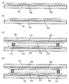
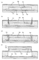
- the separation layer 705 separated from the manufacturing substrate 701 in the step illustrated in FIG. 10D and the substrate 731 are attached to each other with the bonding layer 733, and the bonding layer 733 is cured (FIG. 11A).
- the substrate 731 on the side where the release layer 723 is not provided can be cut with a blade or the like, a cut may be made in the substrate 731, the bonding layer 733, and the peeled layer 725 (see arrow P ⁇ b> 5 in FIG. 11B). .
- part of the layer to be peeled 725 can be removed and a second peeling starting point 743 from the substrate can be formed (see a region surrounded by a dotted line in FIG. 11C).
- the respective manufacturing substrates are peeled off, and the substrates constituting the device to be manufactured can be attached. Therefore, when the layers to be peeled are bonded to each other, manufacturing substrates having low flexibility can be bonded to each other, and the alignment accuracy of the bonding can be improved as compared to the case where the flexible substrates are bonded to each other. it can.
Landscapes
- Engineering & Computer Science (AREA)
- Theoretical Computer Science (AREA)
- Physics & Mathematics (AREA)
- General Engineering & Computer Science (AREA)
- Computer Hardware Design (AREA)
- General Physics & Mathematics (AREA)
- Human Computer Interaction (AREA)
- Devices For Indicating Variable Information By Combining Individual Elements (AREA)
- Optics & Photonics (AREA)
- Computer Networks & Wireless Communication (AREA)
- Quality & Reliability (AREA)
- Electroluminescent Light Sources (AREA)
Abstract
Description
本実施の形態では、本発明の一態様の情報処理装置である、折り曲げ可能なタッチパネルについて、図1乃至図4を参照しながら説明する。タッチパネルは表示部と、タッチセンサを有する。
図1(A)に本発明の一態様の折り曲げ可能なタッチパネルの一状態の断面図を示す。また図1(B)は本発明の一態様の折り曲げ可能なタッチパネルの別の一状態を示す図である。
本実施の形態でパネル基板101として、例えば、タッチパネル300を用いることができる(図3(A)参照)。あるいは、タッチパネル400を用いることができる(図3(B)参照)。タッチパネル300、タッチパネル400はそれぞれ表示部301を有する。
第1の筐体104−1、第2の筐体104−2、ヒンジ105−1、スリット108−1、スリット108−2および端部110を、図4に示す。
本実施の形態では、本発明の一態様の情報処理装置の有する、折り曲げ可能なタッチパネルの構成について、図5を参照しながら説明する。
タッチパネル300は、基板310および基板310に対向する対向基板370を有する(図5(B)参照)。
画素302は、副画素302R、副画素302Gおよび副画素302Bを有する(図5(C)参照)。また、副画素302Rは発光モジュール380Rを備え、副画素302Gは発光モジュール380Gを備え、副画素302Bは発光モジュール380Bを備える。
タッチパネル300は、遮光層367BMを対向基板370に有する。遮光層367BMは、着色層(例えば第1の着色層367R)を囲むように設けられている。
画像信号線駆動回路303s(1)は、トランジスタ303tおよび容量303cを含む。なお、駆動回路は画素回路と同一の工程で同一基板上に形成することができる。
撮像画素308は、光電変換素子308pおよび光電変換素子308pに照射された光を検知するための撮像画素回路を備える。また、撮像画素回路は、トランジスタ308tを含む。
タッチパネル300は、信号を供給することができる配線311を備え、端子319が配線311に設けられている。なお、画像信号および同期信号等の信号を供給することができるFPC309(1)が端子319に電気的に接続されている。端子319に、FPC309(1)とFPC309(2)で分割して接続する構成でも良いし、FPC309と一つで接続する構成でも良い。
本実施の形態では、本発明の一態様の情報処理装置の有するパネル基板に適用することができる折り曲げ可能なタッチパネルの構成について、図6及び図7を参照しながら説明する。
基板590には、タッチセンサ595と、タッチセンサ595と電気的に接続する複数の配線598を備える。複数の配線598は基板590の外周部に引き回され、その一部は端子を構成する。そして、当該端子はFPC509(2)と電気的に接続される。なお、図6(B)では明瞭化のため、基板590の裏面側(基板510と対向する面側)に設けられるタッチセンサ595の電極や配線等を実線で示している。
表示部501は、マトリクス状に配置された複数の画素を備える。画素は表示素子と表示素子を駆動する画素回路を備える。
画素は、副画素502Rを含み、副画素502Rは発光モジュール580Rを備える。
表示部501は、光を射出する方向に遮光層567BMを有する。遮光層567BMは、着色層(例えば第1の着色層567R)を囲むように設けられている。
走査線駆動回路503g(1)は、トランジスタ503tおよび容量503cを含む。なお、駆動回路を画素回路と同一の工程で同一基板上に形成することができる。
表示部501は、信号を供給することができる配線511を備え、端子519が配線511に設けられている。なお、画像信号および同期信号等の信号を供給することができるFPC509(1)が端子519に電気的に接続されている。
様々なトランジスタを表示部501に適用できる。
本実施の形態では、本発明の一態様の情報処理装置に適用することができる折り曲げ可能なタッチパネルの構成について、図8を参照しながら説明する。
表示部501は、マトリクス状に配置された複数の画素を備える。画素は表示素子と表示素子を駆動する画素回路を備える。
画素は、副画素502Rを含み、副画素502Rは発光モジュール580Rを備える。
表示部501は、光を射出する方向に遮光層567BMを有する。遮光層567BMは、着色層(例えば第1の着色層567R)を囲むように設けられている。
タッチセンサ595は、表示部501の基板510側に設けられている(図8(A)参照)。
様々なトランジスタを表示部501に適用できる。
本実施の形態では、他の実施の形態で説明される筐体の、回転方向について説明する。
本実施の形態では、本発明の一態様の情報処理装置や電子機器などに適用することができる折り曲げ可能な装置の作製方法について、図9乃至図11を参照しながら説明する。なお、折り曲げ可能な装置の例としては、表示装置、発光装置、入力装置などがあげられる。入力装置の例としては、タッチセンサ、タッチパネルなどがあげられる。発光装置の例としては、有機ELパネル、照明装置などがあげられる。表示装置の例としては、有機ELパネル、液晶表示装置などがあげられる。なお、表示装置や発光装置の内部に、タッチセンサなどの入力装置の機能が設けられている場合もある。例えば、表示装置や発光装置が有する対向基板(例えば、トランジスタが設けられていない基板)に、タッチセンサが設けられている場合がある。または、表示装置や発光装置が有する素子基板(例えば、トランジスタが設けられている基板)に、タッチセンサが設けられている場合がある。または、表示装置や発光装置が有する対向基板と、表示装置や発光装置が有する素子基板とに、タッチセンサが設けられている場合がある。
本実施の形態では、本発明の一態様の電子機器の構成について、図13を参照しながら説明する。
図13は、折り畳みが可能な電子機器920を示している。図13に示す電子機器920は、筐体921a、筐体921b、表示部922、ヒンジ923、等を有する。表示部922は筐体921a、筐体921bに、組み込まれている。
102 フィルム
103 フィルム
104−1 筐体
104−1A 第1の部分
104−1B 第2の部分
104−2 筐体
104−2A 第1の部分
104−2B 第2の部分
105−1 ヒンジ
106 回路基板
107 FPC
108−1 スリット
108−2 スリット
109 ソケット
110 端部
111 端部
116 支持部
117 支持部
300 タッチパネル
301 表示部
302 画素
302B 副画素
302G 副画素
302R 副画素
302t トランジスタ
303c 容量
303g(1) 走査線駆動回路
303g(2) 撮像画素駆動回路
303s(1) 画像信号線駆動回路
303s(2) 撮像信号線駆動回路
303t トランジスタ
308 撮像画素
308p 光電変換素子
308t トランジスタ
309 FPC
310 基板
310a バリア膜
310b 基板
310c 樹脂層
311 配線
319 端子
321 絶縁膜
328 隔壁
329 スペーサ
350R 発光素子
351R 下部電極
352 上部電極
353 層
353a 発光ユニット
353b 発光ユニット
354 中間層
360 封止材
367BM 遮光層
367p 反射防止層
367R 着色層
370 対向基板
370a バリア膜
370b 基材
370c 樹脂層
380B 発光モジュール
380G 発光モジュール
380R 発光モジュール
400 タッチパネル
401(1) 領域
401(2) 領域
406 線分
407 線分
500 タッチパネル
500B タッチパネル
501 表示部
502R 副画素
502t トランジスタ
503c 容量
503g 走査線駆動回路
503t トランジスタ
509 FPC
510 基板
510a バリア膜
510b 基板
510c 樹脂層
511 配線
519 端子
521 絶縁膜
528 隔壁
550R 発光素子
560 封止材
567BM 遮光層
567p 反射防止層
567R 着色層
570 基板
570a バリア膜
570b 基板
570c 樹脂層
580R 発光モジュール
590 基板
591 電極
592 電極
593 絶縁層
594 配線
595 タッチセンサ
597 樹脂層
598 配線
599 接続層
600A 脆弱部
600B 脆弱部
601 基板
602 基板
603 素子形成領域
604 曲げモーメント
605 中立面
701 作製基板
703 剥離層
705 被剥離層
707 接合層
711 枠状の接合層
721 作製基板
723 剥離層
725 被剥離層
731 基板
733 接合層
741 第1の剥離の起点
743 第2の剥離の起点
920 電子機器
921a 筐体
921b 筐体
922 表示部
923 ヒンジ
Claims (13)
- ヒンジと
第1の筐体と、
第2の筐体と、
パネル基板と、
第1のフィルムと、を有し、
前記ヒンジは、回転軸を備え、
前記第1の筐体は、前記ヒンジを介して、前記回転軸を中心に回転可能に前記第2の筐体と連結され、
前記第1の筐体は、第1のスリットを備え、
前記第2の筐体は、第2のスリットを備え、
前記パネル基板は、前記第1のフィルムと重なる領域を備え、
前記領域は、前記第1のスリットまたは前記第2のスリットの何れか一または両方に収納され、
前記パネル基板、前記第1のフィルム、の何れか一または両方は、前記第2のスリットに沿って摺動可能である情報処理装置。 - 請求項1において、
第2のフィルムを有し、
前記パネル基板は、前記第1のフィルムおよび前記第2のフィルムの間に挟まれる領域を備える情報処理装置。 - 請求項2において、
前記第1のフィルムは、可撓性および可視光に対する透過性を備え、
前記パネル基板は、可撓性および表示領域を備え、
前記第1の筐体は、第1の部分と、第2の部分を有し、
前記第1の部分は、前記表示領域と重なり、
前記第2の部分は、前記第1の部分の周辺部と重なり、
前記第2のフィルムは、前記表示領域および前記第1の部分の間に挟まれ、
前記第2のフィルムは、可撓性を備える情報処理装置。 - 請求項3において、
前記第1のフィルムは、前記第1の筐体の一部に固定され、
前記第1のフィルム、前記第2のフィルムおよび前記パネル基板は、前記第2の筐体を、前記回転軸を中心に前記第1の筐体に対して回転させることにより、前記第2のスリットに沿って摺動可能である情報処理装置。 - 請求項3において、
前記第1のフィルムは、前記第1の筐体に固定され、
前記第1のフィルムは、前記第2の筐体を、前記回転軸を中心に前記第1の筐体に対して回転させることにより、前記第2のスリットに沿って摺動可能であり、
前記第2のフィルムは、前記第1の筐体および前記第2の筐体に固定される情報処理装置。 - 請求項3または請求項4において、
前記第2の筐体は、前記回転軸と平行な端部を備え、
前記第1のフィルムおよび前記パネル基板が、前記第2のスリット内にて摺動し、
前記第1のフィルムは、前記端部から離れ、
前記パネル基板は、前記端部から離れている情報処理装置。 - 請求項1において、
前記第2の筐体を、前記回転軸を中心に前記第1の筐体に対して回転させることにより、
前記第1のフィルムは、前記パネル基板に対し、平面状または凸形状になる情報処理装置。 - 請求項1において、
回路基板を有し、
前記回路基板は、前記パネル基板と電気的に接続され、
前記回路基板は、前記第1の筐体に収納される情報処理装置。 - 請求項1において、
少なくとも1の駆動回路を有し、
前記駆動回路は、前記パネル基板上に設けられ、
前記パネル基板は、前記駆動回路と前記表示領域との間に、湾曲部を備える、
情報処理装置。 - 請求項1において、
前記パネル基板は、画像信号線駆動回路を有し、
前記パネル基板は、前記画像信号線駆動回路および前記表示領域の間に、湾曲部を備える、情報処理装置。 - 請求項1において、
入力部を有し、
前記入力部は、タッチセンサを備え、
前記タッチセンサは、前記表示領域と重なる領域を備える情報処理装置。 - 請求項11において、
第1のフレキシブルプリント基板と、第2のフレキシブルプリント基板と
を有し、
前記第1の筐体は、前記第1のフレキシブルプリント基板および前記第2のフレキシブルプリント基板を収納し、
前記第1のフレキシブルプリント基板は、前記表示領域に制御信号を供給し、
前記第2のフレキシブルプリント基板は、前記タッチセンサに制御信号を供給する情報処理装置。 - 請求項1において、
キーボード、ハードウェアボタン、ポインティングデバイス、照度センサ、撮像装置、音声入力装置、視線入力装置、姿勢検出装置、のうち一以上を含む情報処理装置。
Priority Applications (10)
| Application Number | Priority Date | Filing Date | Title |
|---|---|---|---|
| KR1020197010324A KR102543857B1 (ko) | 2016-10-27 | 2017-10-18 | 정보 처리 장치, 표시 장치, 및 전자 기기 |
| CN202311403649.3A CN117666709A (zh) | 2016-10-27 | 2017-10-18 | 数据处理装置、显示装置以及电子设备 |
| US16/340,227 US11113995B2 (en) | 2016-10-27 | 2017-10-18 | Information processing device, display device, and electronic device |
| JP2018546930A JP6949862B2 (ja) | 2016-10-27 | 2017-10-18 | 情報処理装置 |
| DE112017005427.3T DE112017005427T5 (de) | 2016-10-27 | 2017-10-18 | Informationsverarbeitungsvorrichtung, Anzeigevorrichtung und elektronisches Gerät |
| CN201780063303.XA CN109844684B (zh) | 2016-10-27 | 2017-10-18 | 数据处理装置、显示装置以及电子设备 |
| KR1020247014654A KR20240068763A (ko) | 2016-10-27 | 2017-10-18 | 정보 처리 장치, 표시 장치, 및 전자 기기 |
| KR1020237019603A KR102664173B1 (ko) | 2016-10-27 | 2017-10-18 | 정보 처리 장치, 표시 장치, 및 전자 기기 |
| US17/346,348 US12094368B2 (en) | 2016-10-27 | 2021-06-14 | Information processing device, display device, and electronic device |
| US18/830,873 US20240428710A1 (en) | 2016-10-27 | 2024-09-11 | Information processing device, display device, and electronic device |
Applications Claiming Priority (2)
| Application Number | Priority Date | Filing Date | Title |
|---|---|---|---|
| JP2016-210222 | 2016-10-27 | ||
| JP2016210222 | 2016-10-27 |
Related Child Applications (2)
| Application Number | Title | Priority Date | Filing Date |
|---|---|---|---|
| US16/340,227 A-371-Of-International US11113995B2 (en) | 2016-10-27 | 2017-10-18 | Information processing device, display device, and electronic device |
| US17/346,348 Continuation US12094368B2 (en) | 2016-10-27 | 2021-06-14 | Information processing device, display device, and electronic device |
Publications (1)
| Publication Number | Publication Date |
|---|---|
| WO2018078487A1 true WO2018078487A1 (ja) | 2018-05-03 |
Family
ID=62024454
Family Applications (1)
| Application Number | Title | Priority Date | Filing Date |
|---|---|---|---|
| PCT/IB2017/056459 Ceased WO2018078487A1 (ja) | 2016-10-27 | 2017-10-18 | 情報処理装置、表示装置および電子機器 |
Country Status (6)
| Country | Link |
|---|---|
| US (3) | US11113995B2 (ja) |
| JP (4) | JP6949862B2 (ja) |
| KR (3) | KR102543857B1 (ja) |
| CN (2) | CN117666709A (ja) |
| DE (1) | DE112017005427T5 (ja) |
| WO (1) | WO2018078487A1 (ja) |
Cited By (6)
| Publication number | Priority date | Publication date | Assignee | Title |
|---|---|---|---|---|
| CN109460165A (zh) * | 2018-11-12 | 2019-03-12 | 京东方科技集团股份有限公司 | 触控基板及制作方法、显示面板及制作方法、基板组件 |
| CN109872635A (zh) * | 2019-03-29 | 2019-06-11 | 厦门天马微电子有限公司 | 一种显示装置及其制作方法 |
| JP2020129102A (ja) * | 2019-02-07 | 2020-08-27 | 三星ディスプレイ株式會社Samsung Display Co.,Ltd. | フォルダブル表示装置 |
| JP2021043492A (ja) * | 2019-09-06 | 2021-03-18 | レノボ・シンガポール・プライベート・リミテッド | 電子機器 |
| JP2023513863A (ja) * | 2020-02-24 | 2023-04-04 | 京東方科技集團股▲ふん▼有限公司 | 表示装置及びその製造方法 |
| JP7524418B1 (ja) | 2023-02-24 | 2024-07-29 | 北京小米移動軟件有限公司 | 電子機器 |
Families Citing this family (13)
| Publication number | Priority date | Publication date | Assignee | Title |
|---|---|---|---|---|
| US11342521B2 (en) * | 2018-01-29 | 2022-05-24 | Sharp Kabushiki Kaisha | Display device and method for manufacturing display device |
| KR102454195B1 (ko) * | 2018-05-14 | 2022-10-13 | 삼성디스플레이 주식회사 | 폴더블 표시 장치 |
| KR20260036031A (ko) * | 2018-08-31 | 2026-03-13 | 가부시키가이샤 한도오따이 에네루기 켄큐쇼 | 표시 장치 |
| TWI872058B (zh) | 2019-04-19 | 2025-02-11 | 日商半導體能源研究所股份有限公司 | 撓性構件的支撐工具以及顯示裝置 |
| CN110148358B (zh) * | 2019-06-28 | 2022-01-28 | 京东方科技集团股份有限公司 | 柔性屏的贴合治具和柔性屏的贴合方法 |
| CN114945966A (zh) | 2020-01-10 | 2022-08-26 | 株式会社半导体能源研究所 | 角度调整装置、支撑工具及显示装置 |
| KR102825013B1 (ko) * | 2020-04-28 | 2025-06-27 | 삼성디스플레이 주식회사 | 디지타이저 및 이를 포함하는 표시 장치 |
| KR102827183B1 (ko) * | 2020-06-23 | 2025-07-02 | 삼성디스플레이 주식회사 | 디스플레이 장치 |
| WO2022153627A1 (ja) * | 2021-01-13 | 2022-07-21 | キヤノン電子管デバイス株式会社 | 光電変換基板 |
| EP4550764A4 (en) * | 2022-08-02 | 2025-10-29 | Samsung Electronics Co Ltd | ELECTRONIC DEVICE INCLUDING A PROTECTIVE STRUCTURE FOR A FLEXIBLE SCREEN |
| JP7366207B1 (ja) * | 2022-08-03 | 2023-10-20 | レノボ・シンガポール・プライベート・リミテッド | 電子機器 |
| CN118553156A (zh) * | 2023-02-24 | 2024-08-27 | 北京小米移动软件有限公司 | 电子设备 |
| CN118554102A (zh) * | 2023-02-24 | 2024-08-27 | 北京小米移动软件有限公司 | 电子设备 |
Citations (3)
| Publication number | Priority date | Publication date | Assignee | Title |
|---|---|---|---|---|
| JP2013050547A (ja) * | 2011-08-30 | 2013-03-14 | Canon Inc | 表示装置 |
| JP2015062059A (ja) * | 2013-08-20 | 2015-04-02 | 株式会社半導体エネルギー研究所 | 表示装置 |
| JP2015135484A (ja) * | 2013-12-20 | 2015-07-27 | 株式会社半導体エネルギー研究所 | 半導体装置 |
Family Cites Families (17)
| Publication number | Priority date | Publication date | Assignee | Title |
|---|---|---|---|---|
| JP2003292828A (ja) * | 2002-03-29 | 2003-10-15 | Lintec Corp | ハードコート剤及びハードコートフィルム |
| JP2005114759A (ja) * | 2003-10-02 | 2005-04-28 | Canon Inc | ディスプレイ装置、携帯電話機、及び電子機器 |
| JP5446790B2 (ja) | 2009-12-02 | 2014-03-19 | セイコーエプソン株式会社 | 電気光学装置および電子機器 |
| KR102079188B1 (ko) | 2012-05-09 | 2020-02-19 | 가부시키가이샤 한도오따이 에네루기 켄큐쇼 | 발광 장치 및 전자 기기 |
| KR101911047B1 (ko) * | 2012-07-25 | 2018-10-24 | 삼성디스플레이 주식회사 | 케이스 및 표시 장치 |
| WO2014175296A1 (en) * | 2013-04-24 | 2014-10-30 | Semiconductor Energy Laboratory Co., Ltd. | Display device |
| KR102790055B1 (ko) * | 2013-07-12 | 2025-04-03 | 가부시키가이샤 한도오따이 에네루기 켄큐쇼 | 발광 장치 |
| TWI643056B (zh) * | 2013-07-22 | 2018-12-01 | 日商半導體能源研究所股份有限公司 | 發光裝置 |
| KR20200139848A (ko) | 2013-08-30 | 2020-12-14 | 가부시키가이샤 한도오따이 에네루기 켄큐쇼 | 표시 장치 |
| US9588549B2 (en) * | 2014-02-28 | 2017-03-07 | Semiconductor Energy Laboratory Co., Ltd. | Electronic device |
| US10399310B2 (en) * | 2015-07-22 | 2019-09-03 | Sumitomo Chemical Company, Limited | Resin film, laminate, optical member, gas barrier material and touch sensor substrate |
| US9947882B2 (en) * | 2015-09-25 | 2018-04-17 | Apple Inc. | Electronic devices with robust flexible displays |
| JP6918560B2 (ja) * | 2016-04-28 | 2021-08-11 | 株式会社半導体エネルギー研究所 | 情報処理装置 |
| WO2018016446A1 (ja) * | 2016-07-21 | 2018-01-25 | シャープ株式会社 | 有機el表示装置 |
| JP2018081186A (ja) * | 2016-11-16 | 2018-05-24 | 株式会社半導体エネルギー研究所 | 情報処理装置、表示装置および電子機器 |
| US10303218B2 (en) * | 2017-02-01 | 2019-05-28 | Apple Inc. | Foldable cover and display for an electronic device |
| EP4004073A1 (en) * | 2019-07-25 | 2022-06-01 | Nanogate SE | Mouldable, formable and chemically resistant hard coat for polymer film |
-
2017
- 2017-10-18 KR KR1020197010324A patent/KR102543857B1/ko active Active
- 2017-10-18 DE DE112017005427.3T patent/DE112017005427T5/de active Pending
- 2017-10-18 KR KR1020247014654A patent/KR20240068763A/ko active Pending
- 2017-10-18 KR KR1020237019603A patent/KR102664173B1/ko active Active
- 2017-10-18 JP JP2018546930A patent/JP6949862B2/ja active Active
- 2017-10-18 US US16/340,227 patent/US11113995B2/en active Active
- 2017-10-18 CN CN202311403649.3A patent/CN117666709A/zh active Pending
- 2017-10-18 CN CN201780063303.XA patent/CN109844684B/zh active Active
- 2017-10-18 WO PCT/IB2017/056459 patent/WO2018078487A1/ja not_active Ceased
-
2021
- 2021-06-14 US US17/346,348 patent/US12094368B2/en active Active
- 2021-09-22 JP JP2021154168A patent/JP2022003557A/ja not_active Withdrawn
-
2023
- 2023-07-10 JP JP2023113233A patent/JP2023126341A/ja not_active Withdrawn
-
2024
- 2024-09-11 US US18/830,873 patent/US20240428710A1/en active Pending
-
2025
- 2025-04-07 JP JP2025063080A patent/JP2025106421A/ja active Pending
Patent Citations (3)
| Publication number | Priority date | Publication date | Assignee | Title |
|---|---|---|---|---|
| JP2013050547A (ja) * | 2011-08-30 | 2013-03-14 | Canon Inc | 表示装置 |
| JP2015062059A (ja) * | 2013-08-20 | 2015-04-02 | 株式会社半導体エネルギー研究所 | 表示装置 |
| JP2015135484A (ja) * | 2013-12-20 | 2015-07-27 | 株式会社半導体エネルギー研究所 | 半導体装置 |
Cited By (10)
| Publication number | Priority date | Publication date | Assignee | Title |
|---|---|---|---|---|
| CN109460165A (zh) * | 2018-11-12 | 2019-03-12 | 京东方科技集团股份有限公司 | 触控基板及制作方法、显示面板及制作方法、基板组件 |
| JP2020129102A (ja) * | 2019-02-07 | 2020-08-27 | 三星ディスプレイ株式會社Samsung Display Co.,Ltd. | フォルダブル表示装置 |
| JP7272845B2 (ja) | 2019-02-07 | 2023-05-12 | 三星ディスプレイ株式會社 | フォルダブル表示装置 |
| CN109872635A (zh) * | 2019-03-29 | 2019-06-11 | 厦门天马微电子有限公司 | 一种显示装置及其制作方法 |
| JP2021043492A (ja) * | 2019-09-06 | 2021-03-18 | レノボ・シンガポール・プライベート・リミテッド | 電子機器 |
| JP2023513863A (ja) * | 2020-02-24 | 2023-04-04 | 京東方科技集團股▲ふん▼有限公司 | 表示装置及びその製造方法 |
| JP7641954B2 (ja) | 2020-02-24 | 2025-03-07 | 京東方科技集團股▲ふん▼有限公司 | 表示装置及びその製造方法 |
| JP7524418B1 (ja) | 2023-02-24 | 2024-07-29 | 北京小米移動軟件有限公司 | 電子機器 |
| JP2024120822A (ja) * | 2023-02-24 | 2024-09-05 | 北京小米移動軟件有限公司 | 電子機器 |
| US12339709B2 (en) | 2023-02-24 | 2025-06-24 | Beijing Xiaomi Mobile Software Co., Ltd. | Electronic device |
Also Published As
| Publication number | Publication date |
|---|---|
| JP2023126341A (ja) | 2023-09-07 |
| JP2025106421A (ja) | 2025-07-15 |
| KR102664173B1 (ko) | 2024-05-10 |
| DE112017005427T5 (de) | 2019-07-25 |
| KR20230088523A (ko) | 2023-06-19 |
| JPWO2018078487A1 (ja) | 2019-09-05 |
| CN109844684B (zh) | 2023-11-17 |
| US20210304643A1 (en) | 2021-09-30 |
| KR20190067798A (ko) | 2019-06-17 |
| US11113995B2 (en) | 2021-09-07 |
| CN109844684A (zh) | 2019-06-04 |
| US12094368B2 (en) | 2024-09-17 |
| KR102543857B1 (ko) | 2023-06-14 |
| JP6949862B2 (ja) | 2021-10-13 |
| US20200043382A1 (en) | 2020-02-06 |
| JP2022003557A (ja) | 2022-01-11 |
| US20240428710A1 (en) | 2024-12-26 |
| KR20240068763A (ko) | 2024-05-17 |
| CN117666709A (zh) | 2024-03-08 |
Similar Documents
| Publication | Publication Date | Title |
|---|---|---|
| JP7290691B2 (ja) | 情報処理装置 | |
| JP6949862B2 (ja) | 情報処理装置 | |
| JP7543498B2 (ja) | 表示装置 | |
| TWI772144B (zh) | 資料處理裝置及資料處理裝置的驅動方法 | |
| JP2018081186A (ja) | 情報処理装置、表示装置および電子機器 |
Legal Events
| Date | Code | Title | Description |
|---|---|---|---|
| 121 | Ep: the epo has been informed by wipo that ep was designated in this application |
Ref document number: 17866347 Country of ref document: EP Kind code of ref document: A1 |
|
| ENP | Entry into the national phase |
Ref document number: 2018546930 Country of ref document: JP Kind code of ref document: A |
|
| ENP | Entry into the national phase |
Ref document number: 20197010324 Country of ref document: KR Kind code of ref document: A |
|
| 122 | Ep: pct application non-entry in european phase |
Ref document number: 17866347 Country of ref document: EP Kind code of ref document: A1 |