WO2018074281A1 - アニール被処理体の製造方法、レーザアニール基台およびレーザアニール処理装置 - Google Patents
アニール被処理体の製造方法、レーザアニール基台およびレーザアニール処理装置 Download PDFInfo
- Publication number
- WO2018074281A1 WO2018074281A1 PCT/JP2017/036656 JP2017036656W WO2018074281A1 WO 2018074281 A1 WO2018074281 A1 WO 2018074281A1 JP 2017036656 W JP2017036656 W JP 2017036656W WO 2018074281 A1 WO2018074281 A1 WO 2018074281A1
- Authority
- WO
- WIPO (PCT)
- Prior art keywords
- processed
- cam member
- laser
- laser light
- laser beam
- Prior art date
- Legal status (The legal status is an assumption and is not a legal conclusion. Google has not performed a legal analysis and makes no representation as to the accuracy of the status listed.)
- Ceased
Links
Images

Classifications
-
- B—PERFORMING OPERATIONS; TRANSPORTING
- B23—MACHINE TOOLS; METAL-WORKING NOT OTHERWISE PROVIDED FOR
- B23K—SOLDERING OR UNSOLDERING; WELDING; CLADDING OR PLATING BY SOLDERING OR WELDING; CUTTING BY APPLYING HEAT LOCALLY, e.g. FLAME CUTTING; WORKING BY LASER BEAM
- B23K26/00—Working by laser beam, e.g. welding, cutting or boring
- B23K26/08—Devices involving relative movement between laser beam and workpiece
- B23K26/083—Devices involving movement of the workpiece in at least one axial direction
-
- B—PERFORMING OPERATIONS; TRANSPORTING
- B23—MACHINE TOOLS; METAL-WORKING NOT OTHERWISE PROVIDED FOR
- B23K—SOLDERING OR UNSOLDERING; WELDING; CLADDING OR PLATING BY SOLDERING OR WELDING; CUTTING BY APPLYING HEAT LOCALLY, e.g. FLAME CUTTING; WORKING BY LASER BEAM
- B23K26/00—Working by laser beam, e.g. welding, cutting or boring
- B23K26/08—Devices involving relative movement between laser beam and workpiece
- B23K26/10—Devices involving relative movement between laser beam and workpiece using a fixed support, i.e. involving moving the laser beam
- B23K26/103—Devices involving relative movement between laser beam and workpiece using a fixed support, i.e. involving moving the laser beam the laser beam rotating around the fixed workpiece
-
- B—PERFORMING OPERATIONS; TRANSPORTING
- B23—MACHINE TOOLS; METAL-WORKING NOT OTHERWISE PROVIDED FOR
- B23K—SOLDERING OR UNSOLDERING; WELDING; CLADDING OR PLATING BY SOLDERING OR WELDING; CUTTING BY APPLYING HEAT LOCALLY, e.g. FLAME CUTTING; WORKING BY LASER BEAM
- B23K26/00—Working by laser beam, e.g. welding, cutting or boring
- B23K26/08—Devices involving relative movement between laser beam and workpiece
- B23K26/082—Scanning systems, i.e. devices involving movement of the laser beam relative to the laser head
-
- H—ELECTRICITY
- H10—SEMICONDUCTOR DEVICES; ELECTRIC SOLID-STATE DEVICES NOT OTHERWISE PROVIDED FOR
- H10P—GENERIC PROCESSES OR APPARATUS FOR THE MANUFACTURE OR TREATMENT OF DEVICES COVERED BY CLASS H10
- H10P14/00—Formation of materials, e.g. in the shape of layers or pillars
- H10P14/20—Formation of materials, e.g. in the shape of layers or pillars of semiconductor materials
-
- H—ELECTRICITY
- H10—SEMICONDUCTOR DEVICES; ELECTRIC SOLID-STATE DEVICES NOT OTHERWISE PROVIDED FOR
- H10P—GENERIC PROCESSES OR APPARATUS FOR THE MANUFACTURE OR TREATMENT OF DEVICES COVERED BY CLASS H10
- H10P34/00—Irradiation with electromagnetic or particle radiation of wafers, substrates or parts of devices
- H10P34/40—Irradiation with electromagnetic or particle radiation of wafers, substrates or parts of devices with high-energy radiation
- H10P34/42—Irradiation with electromagnetic or particle radiation of wafers, substrates or parts of devices with high-energy radiation with electromagnetic radiation, e.g. laser annealing
-
- H—ELECTRICITY
- H10—SEMICONDUCTOR DEVICES; ELECTRIC SOLID-STATE DEVICES NOT OTHERWISE PROVIDED FOR
- H10P—GENERIC PROCESSES OR APPARATUS FOR THE MANUFACTURE OR TREATMENT OF DEVICES COVERED BY CLASS H10
- H10P72/00—Handling or holding of wafers, substrates or devices during manufacture or treatment thereof
- H10P72/70—Handling or holding of wafers, substrates or devices during manufacture or treatment thereof for supporting or gripping
Definitions
- the present invention relates to a method for manufacturing an annealed object that has been annealed by laser light irradiation, a laser annealing base on which the object is supported, and a laser annealing apparatus that performs laser annealing on the object. Is.
- the laser processing object is placed on the sample table and irradiated with laser light, and the sample table is created according to the size of the laser processing object. is doing.
- the size of laser processing objects has been increasing, and the sample stage has become larger as the size of laser processing objects increases. For this reason, weight, surface flatness, shaking during movement, variation in speed during movement, and the like are deteriorated, making it difficult to maintain specifications required for laser processing.
- the laser annealing processing apparatus is used for high-performance displays such as OLEDs and high-definition LCDs, and has a higher required performance. Necessary for laser processing in laser processing of large substrates, particularly substrates of 2 m or more.
- the sample stage it is difficult for the sample stage to satisfy the specifications. For example, if the surface flatness of the laser processing object is impaired, the relationship between the focal point and the irradiation position when the laser light is irradiated may be shifted, and the annealing effect may be uneven depending on the position.
- Patent Document 1 includes a roller transport unit for transporting an object to be processed having a plurality of rollers, and a laser processing apparatus for processing the object to be processed. And an autofocus mechanism, and the autofocus mechanism is connected to the laser oscillator so that the surface of the object to be processed can be irradiated and processed by the laser beam emitted from the laser oscillator via the autofocus mechanism.
- a manufacturing apparatus has been proposed.
- Patent Document 1 it is not easy to accurately auto-focus a laser beam on a target object whose structure is complicated and whose flat surface continuously changes.
- the laser beam is irradiated in a line beam shape, it is difficult to adjust the focal position in the entire major axis direction by autofocus.
- An object of the present invention is to provide a laser annealing base and a laser annealing treatment apparatus.
- the first invention of the present invention is a method of manufacturing an annealed object that performs annealing of the object to be processed by irradiating the object with laser light.
- rotation is performed at least in a laser light irradiation region on the object to be processed.
- the object to be processed is supported by a cam member whose upper end height position is adjusted by the position.
- the laser beam is irradiated while being scanned relatively to the object to be processed, and the support In the step, with the relative scanning of the laser light, the cam member supports the object to be processed at least in the laser light irradiation region.
- a method for manufacturing an annealed object to be measured in the first or second aspect of the present invention the measuring step of measuring the height position of the object to be processed in the laser light irradiation region. And a height position adjusting step for determining a rotational position of the cam member based on the height position.
- a laser annealing base comprising: a support portion that supports a workpiece to be irradiated with laser light, wherein the support portion corresponds to at least an irradiation region where the laser beam is irradiated to the workpiece. And a cam member that supports the object to be processed from the lower surface side, and a cam rotation drive unit that rotates the cam member.
- a laser annealing base includes the scanning device according to the fourth aspect of the present invention, wherein the processing target is moved relative to the laser light to scan the laser light,
- the cam member performs the support with respect to the object to be processed at least in a laser light irradiation region in accordance with the scanning of the laser light.
- the laser annealing base according to the fifth aspect of the present invention, wherein the cam member has a fixed installation position with respect to the irradiation position of the laser beam, and has no cam member.
- a support part is movable with the said to-be-processed object, It is characterized by the above-mentioned.
- the laser annealing base according to any one of the fourth to sixth aspects, wherein the height position of the object to be processed is measured at least corresponding to the irradiation region irradiated with the laser beam.
- a control unit that controls the cam rotation driving unit, the control unit receiving the measurement result of the measurement device and adjusting the rotational position of the cam member based on the measurement result. And controlling to adjust the object to be processed to a predetermined height position.
- the laser annealing base according to an eighth aspect of the present invention is the laser annealing base according to the sixth aspect of the present invention, wherein the cam member includes a plurality of cam members in the lower surface direction of the object to be processed, The rotation position can be changed independently for each group of cam members.
- the cam member contacts the object to be processed and supports the object to be processed. It is characterized by.
- the laser annealing base of the tenth aspect of the present invention is characterized in that, in any of the fourth to ninth aspects of the present invention, the cam member supports the object to be processed by gas levitation. .
- the laser annealing base of the eleventh aspect of the present invention is characterized in that, in any of the tenth aspects of the present invention, the cam member is made of a porous material at least on the gas blowing surface side.
- the cam member has a gas blown from the cam member regardless of the rotational position of the cam member. It has the blowing part which hits a lower surface right above.
- a laser annealing base of a thirteenth aspect of the present invention is the laser annealing base according to any one of the seventh to twelfth aspects of the present invention, wherein the laser light is shaped into a line beam shape and irradiated onto the object to be processed.
- a plurality of the cam members are arranged along the long axis direction of the laser beam.
- a laser annealing treatment apparatus provides a laser annealing base according to any one of the fourth to thirteenth aspects of the present invention, a laser light source that outputs a laser beam, and the laser beam that guides the laser beam. And an optical system for irradiating the target object supported by the annealing base with the laser beam.
- an object to be processed such as a laser processing object used in a liquid crystal display or an organic EL display.
- an object to be processed such as a laser processing object used in a liquid crystal display or an organic EL display.
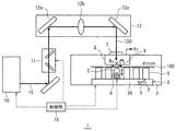
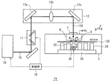
- FIG. 1 It is the schematic which shows the annealing base of one Embodiment of this invention, and the laser annealing processing apparatus of one Embodiment provided with this annealing base.
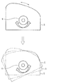
- the figure which shows a cam member and a drive motor and the figure which shows the state which the cam member rotated.
- the laser annealing processing apparatus 1 includes a processing chamber 2, and a scanning device 3 is provided in the processing chamber 2.
- the scanning device 3 includes a scanning direction moving unit 30 that can move in the X direction (scanning direction).
- a plurality of support units 4 that move together with the scanning direction moving unit 30 are provided.
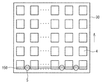
- a plurality of support parts 4 are arranged in the X direction and the Y direction at intervals, and the top part is an installation part on which the object to be processed is placed.
- the support part 4 is formed in columnar shape, and the top surface is an installation part.
- the scanning direction moving unit 30 is movable along a guide or the like that extends in the X direction on the base of the processing chamber 2 and is driven by a motor or the like (not shown) to move the support unit 4 to the laser beam. It can be moved in the scanning direction. Further, the scanning direction moving unit 30 may move in the Y direction to change the irradiation position.
- the cam member 5 is disposed along the Y direction (direction orthogonal to the scanning direction) below the irradiation region irradiated with the laser light.
- the cam member 5 constitutes a part of the support portion of the present invention.
- a plurality of cam members 5 are positioned at intervals along the Y direction so as not to be positioned on the X direction line in which the support portion 4 moves. Thereby, when the support part 4 moves with the scanning direction moving part 30, it does not interfere with the cam member 5.
- Each cam member 5 is connected to a drive motor 6 that adjusts the rotational position of the cam member 5.
- a stepping motor or the like can be used as the drive motor 6.
- the drive motor 6 corresponds to a cam rotation drive unit of the present invention.
- the type of the cam rotation driving unit is not particularly limited.
- the cam member 5 supports the object to be processed on its top side, but the position and height of the top portion can be changed by the rotation of the cam member 5.
- the rotational position may be changed to an arbitrary position, or a plurality of predetermined positions may be selected and changed.
- the scanning device 3 including the scanning direction moving unit 30 and the guide, the support unit 4, the cam member 5, and the drive motor 6 are components of the annealing base of the present invention. Note that it is not essential for the present invention to have a plurality of cam members 5.
- the processing chamber 2 is provided with an introduction window 7 for introducing a line beam from the outside.
- an injection cylinder 8 is provided below the introduction window 7 so as to surround the optical path of the laser beam 150, and a transmitting portion such as a hole through which the laser light is transmitted to the lower surface side of the injection cylinder 8. Is formed.
- a height measuring device 9 is provided for measuring the upper surface height of the object to be processed which is located below and moves.
- the height measuring device 9 includes one that measures the height of the measurement point continuously or intermittently.
- the configuration of the height measuring device 9 is not particularly limited.
- the height of the object to be processed is measured using an optical sensor or the like.
- the height measuring device 9 corresponds to the measuring device of the present invention.
- the height measuring device 9 may be any device as long as it can measure the height position of the object to be processed at or near the irradiation position of the laser beam 150, and is not limited to the injection cylinder 8 and can be installed at an appropriate position.
- measurement may be performed at a plurality of positions.
- the irradiated laser beam is a line beam, it is desirable to measure the position of the object to be processed along the minor axis direction (Y direction), and the height measuring device 9 is used using a line sensor or a plurality of sensors. Can be.
- a semiconductor substrate 100 in which an amorphous silicon film or the like is formed on a glass substrate or the like is installed at the center of the scanning direction moving unit 30.
- the semiconductor substrate 100 corresponds to the object to be processed of the present invention.
- the object to be processed is not limited to a semiconductor substrate.
- the laser annealing apparatus 1 according to the first embodiment will be described as related to laser annealing for crystallizing an amorphous film by laser processing.
- the content of laser processing is crystal of an amorphous film.
- a non-single-crystal semiconductor film may be single-crystallized or a crystalline semiconductor film may be modified.
- it may be related to other processing, and as described above, the object to be processed is not limited to a specific one.
- a laser light source 10 is installed outside the processing chamber 2.
- the laser light source 10 may output either laser light of pulsed laser light or continuous wave laser light, and the present invention is not limited to any one, and uses a plurality of laser light sources. It may be. However, in this Embodiment 1, what uses a pulsed laser beam with a higher energy density is suitable.
- examples of the pulsed laser beam include those having a wavelength of 400 nm or less and a pulse half width of 200 nsec or less.
- the pulsed laser light 15 output from the laser light source 10 is adjusted in energy density by an attenuator 11 as necessary, and is formed into a line beam shape by an optical system 12 including a reflection mirror 12a, a condenser lens 12b, a reflection mirror 12c, and the like. Then, the laser beam 150 is emitted.
- the optical member which comprises the optical system 12 is not limited to the said prescription
- the cross-sectional shape of the line beam shape is not particularly limited.
- a cross-sectional shape having a minor axis width of 100 ⁇ m to 500 ⁇ m and a major axis width of 370 to 1300 mm on the irradiation surface of the object to be processed is used. It can be illustrated.
- the beam cross-sectional shape of the laser beam 150 applied to the object to be processed is described as a line beam shape.
- the present invention is not limited to this, but is a spot shape or a circular shape. It is also possible to adopt an appropriate irradiation shape such as a rectangular shape.
- the laser annealing apparatus 1 includes a control unit 16 that controls at least the scanning device 3, the drive motor 6, the laser light source 10, and the attenuator 11.
- the control unit 16 can be configured by a CPU, a program that causes the CPU to perform a predetermined operation, a storage unit, and the like.
- the scanning device 3 can move the scanning direction moving unit 30 together with the support unit 4 at a predetermined speed under the control of the control unit 16.
- the predetermined speed is not particularly limited, for example, 1 to 100 mm / second can be exemplified.
- the scanning position may be changed by moving the scanning device 3 in the Y direction.
- the control unit 16 can control the laser light source 10 to output the laser light 15 with a predetermined output, and further control the attenuator 11 to irradiate the laser light 150 with a predetermined energy density on the object to be processed. Can be controlled.
- the energy density on the object to be processed can be set to an appropriate value according to the purpose of annealing.
- FIG. 2 shows a front view of one of the cam members 5 as viewed in the Y direction, and the upper surface has an inclined curved shape.
- the cam member 5 has a rotation shaft along the Y direction on the lower side, and a drive motor 6 is connected to the rotation shaft, and the drive motor 6 can rotate the cam member 5 along the rotation shaft. it can.
- the cam member 5 rotates, the maximum height position changes as shown in the lower diagram of FIG.
- the semiconductor substrate 100 is supported on the upper surface side of the cam member 5, the height position of the semiconductor substrate 100 on the cam member 5 varies depending on the rotational position of the cam member 5.
- the cam member 5 By arranging the cam member 5 directly below or in the vicinity of the laser beam 150, the height position of the semiconductor substrate 100 irradiated with the laser beam 150 can be adjusted by the rotation operation of the cam member 5.
- the upper surface of the cam member 5 it is not essential that the upper surface of the cam member 5 has a curved shape, and the inclination angle may be changed stepwise.
- the pulse is oscillated at a predetermined repetition frequency under the control of the control unit 16, and the laser light 15 is output at a predetermined output.
- the laser beam 15 include those having a wavelength of 400 nm or less and a pulse half width of 200 nsec or less.
- the pulse energy density of the laser light 15 is adjusted by the attenuator 11 controlled by the control unit 16.
- the attenuator 11 is set to a predetermined attenuation rate, and the attenuation rate is adjusted so that an irradiation pulse energy density optimum for crystallization can be obtained on the irradiation surface of the semiconductor substrate 100.
- the energy density can be adjusted to 250 to 500 mJ / cm 2 on the irradiated surface.
- the laser beam 15 that has passed through the attenuator 11 is shaped into a line beam shape by the optical system 12 and the short axis width is condensed, and is introduced into the introduction window 6 provided in the processing chamber 2 as the line beam laser beam 150.
- the line beam is shaped to have a length of 370 to 1300 mm on the long axis side and a length of 100 ⁇ m to 500 ⁇ m on the short axis side.
- the semiconductor substrate 100 By moving the semiconductor substrate 100 at a predetermined scanning speed by the scanning device 3 controlled by the control unit 16, the semiconductor substrate 100 can be irradiated while scanning the line beam laser light 150 relative to the semiconductor substrate 100. it can.
- the scanning speed at this time is, for example, in the range of 1 to 100 mm / second.
- the scanning speed is not limited to a specific one.
- the scanning pitch is not limited to a specific numerical value, but can be in the range of 5 to 15 ⁇ m, for example.
- the laser beam can be moved relative to the semiconductor substrate 100 by moving the laser beam.
- the movement of the laser beam can be performed, for example, by moving an optical fiber that passes the laser beam.
- the height position of the semiconductor substrate 100 is measured by the height measuring device 9, and the measurement result is sent to the control unit 16. Based on the measurement result, the control unit 16 controls the drive motor 6 to adjust the rotational position of the cam member 5 so that the semiconductor substrate 100 is at a predetermined height position.
- the height measuring device 9 reflects the measurement result in the rotational position adjustment of the cam member 5 and reflects the laser beam 150 on the upstream side in the transport direction of the semiconductor substrate 100 by the scanning device 3 from the position of the cam member 5. It is desirable to arrange it at a position as close to the cam member 5 as possible.
- the predetermined height position may be a constant value or may be a value determined according to the scanning direction of the semiconductor substrate 100. In short, the height of the semiconductor substrate 100 is adjusted to a predetermined height position. I can do it.
- movement may be performed with the whole or a part cam member 5, and you may enable it to adjust a rotation position separately.
- the measurement result measured by the height measuring device 9 can be used at a position corresponding to the position of each cam member 5, and the minor axis direction (Y direction) can be used. Can be adjusted to a uniform height position.
- the height measuring device 9 may measure the height position continuously in the Y direction, or may measure the height position at a plurality of locations.
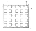
- FIG. 3 shows a state where the semiconductor substrate 100 has reached the cam member 5 on the tip side in the X direction when the semiconductor substrate 100 moves by the scanning direction moving unit 30.
- the illustration of the semiconductor substrate 100 is omitted.
- the tip end side in the X direction of the semiconductor substrate 100 is adjusted to a predetermined height by the rotation of the cam member 5, and the laser beam 150 is irradiated at an appropriate focal position to perform a good annealing process.
- the semiconductor substrate 100 is irradiated with the laser beam 150 at an appropriate focal position while being moved in the X direction by the scanning direction moving unit 30.
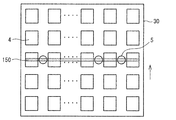
- FIG. 4 shows a state in which the semiconductor substrate 100 is moved and the middle of the semiconductor substrate 100 in the X direction is positioned on the cam member 5 and the height is adjusted.
- FIG. 5 shows the movement of the semiconductor substrate 100. Shows a state in which the rear end side in the X direction of the semiconductor substrate 100 is positioned on the cam member 5 and the height is adjusted. During this time, the cam member 5 is in a fixed position, and the height of the semiconductor substrate 100 is adjusted at the same position with respect to the laser beam 150 whose irradiation position is fixed. If the second line is irradiated in the scanning direction, the semiconductor substrate 100 is moved in the lateral direction by a moving device (not shown) after the first line is completed. The above-described movement of the semiconductor substrate and laser light irradiation are performed on the semiconductor substrate moved in the lateral direction. When the entire glass surface of the semiconductor substrate can be processed, the next substrate is processed.
- the cam member 5 has been described as having a rotation axis along the Y direction.
- the cam member 5 may have a rotation axis inclined in the horizontal plane direction with respect to the X direction and the Y direction.
- it may have a rotating shaft inclined with respect to the vertical direction, may have a plurality of rotating shafts, and each of the rotating shafts can be adjusted for rotation.
- the cam member 5 is rotated by a free rotating shaft. It may be possible to adjust.
- the cam member 5 directly contacts the semiconductor substrate 100 to adjust the height position.
- the semiconductor substrate 100 may be slid on the cam member 5, or the semiconductor member 100 may be moved by providing a rotating roller or the like on the cam member 5. Further, the cam member 5 may be rotated when moving to the semiconductor substrate 100 so that contact with the semiconductor substrate 100 is temporarily released.
- the height position of the semiconductor substrate 100 can be easily and accurately adjusted by the cam member 5, the semiconductor substrate 100 and the focal position of the laser beam have an appropriate positional relationship, and the annealing process is good. Can be done.
- the entire support unit may move without dividing the moving side of the scanning device.
- the plurality of support portions arranged in the X direction have a cam member structure, and the cam member 5 corresponding to the irradiation region of the laser beam 150 as the semiconductor substrate 100 is moved by the scanning device 3.
- the height of the semiconductor substrate 100 can be adjusted by rotating 5.
- the semiconductor substrate 100 is pressed and directly supported by the support portion 4 and the cam member 5, but the semiconductor substrate is floated and supported by the support portion by jetting gas upward. It can be set as a structure.
- the second embodiment will be described below.
- FIG. 6 shows a laser processing apparatus according to Embodiment 2, which is another embodiment.
- symbol is attached
- the support unit fixing device 20 is installed in the processing chamber 2, and a plurality of support units 24 are installed and fixed on the support unit fixing device 20 along the X direction and the Y direction.
- a cam member 25 is arranged along the Y direction below the irradiation position where the laser beam 150 is irradiated.
- a drive motor 26 is connected to the rotation shaft of the cam member 25, and the drive motor 26 corresponds to the rotation drive unit of the present invention.
- the semiconductor substrate 100 is levitated by a predetermined amount of height from the blowing position by blowing a floating gas upward. Further, in the cam member 25, the blowing position is set according to the rotational position, and the blowing is set so that gas is blown out from the cam member 25 as directly as possible.
- the type of the levitation gas is not particularly limited in the present invention, but for example, an inert gas such as nitrogen can be used.
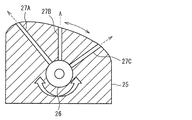
- FIG. 7 shows an example of the cam member 25, which has a porous structure provided with three outlets 27A, 27B, and 27C.
- a valve structure is provided at the air outlet, or the connection of the air outlet passage is switched so that the gas is blown out only from the air outlet that blows the gas directly upward according to the rotational position of the cam member 25. be able to.
- the cam member 25 rotates, the semiconductor substrate 100 can be lifted at a predetermined height from the blowout port located immediately above, and the height of the semiconductor substrate 100 can be adjusted.
- movement may be performed with the whole or one part cam member 25, and you may enable it to adjust a rotation position separately.
- the measurement results measured by the height measuring device 9 can be used at positions corresponding to the positions of the cam members 25, respectively.
- the height measuring device 9 may measure the height position continuously in the Y direction, or may measure the height position at a plurality of locations.
- the cam member 25 is described as having a rotation axis along the Y direction.
- the cam member 25 may have a rotation axis inclined in the horizontal plane direction with respect to the X direction and the Y direction.
- it may have a rotating shaft inclined with respect to the vertical direction, and may have a plurality of rotating shafts, and each of the rotating shafts can be adjusted for rotation, and the cam member 25 is rotated by a free rotating shaft. It may be possible to adjust.
- the mechanism for floating the object to be processed when used, it is not necessary to move the support portion side. Further, it is possible to eliminate the influence of reflection from the lower side in the laser light irradiation region. Furthermore, since the object to be processed does not come into contact with the support portion, generation of particles and static electricity can be suppressed, and processing quality can be improved. Moreover, in the said embodiment, since the height of a blower outlet can be adjusted with a cam member, the amount of gas blowout can be decreased. In the gas blowing, when the flying height is increased, the object to be processed that has floated the gas easily shakes, but according to the present embodiment, the shaking can be suppressed.
- FIG. 8 shows a state in which a laser beam 150 is irradiated on a semiconductor substrate (not shown) that has floated gas.
- the semiconductor substrate 100 can be moved by extruding the semiconductor substrate 100 or using a moving device (not shown) that holds and moves the semiconductor substrate 100.
- the height of the semiconductor substrate 100 is adjusted by the cam member 25 in the irradiation region, and the laser beam 150 is irradiated with an appropriate positional relationship with the focal position of the laser beam 150, and a good annealing process is performed.
- the structure other than the cam member 25 can be moved, and the gas floating can be performed only by the cam member 25. It may be.
Landscapes
- Physics & Mathematics (AREA)
- Optics & Photonics (AREA)
- Engineering & Computer Science (AREA)
- Plasma & Fusion (AREA)
- Mechanical Engineering (AREA)
- Recrystallisation Techniques (AREA)
- Laser Beam Processing (AREA)
- Electromagnetism (AREA)
- Container, Conveyance, Adherence, Positioning, Of Wafer (AREA)
Abstract
被処理体にレーザ光を照射して前記被処理体のアニールを行うアニール被処理体の製造方法において、被処理体を支持する支持ステップと、支持された被処理体に前記レーザ光を照射する照射ステップとを有し、前記支持ステップでは、少なくとも前記被処理体に対するレーザ光の照射領域において、回転位置により上端高さ位置を調整したカム部材によって前記被処理体を支持する。
Description
この発明は、レーザ光の照射によりアニール処理が施されたアニール被処理体の製造方法、前記被処理体が支持されるレーザアニール基台および被処理体にレーザアニール処理を行うレーザアニール処理装置に関するものである。
従来のレーザアニール処理装置では、レーザアニール処理を行う際に、レーザ加工対象物を試料台上に設置してレーザ光を照射しており、レーザ加工対象物の大きさに合わせて試料台を作成している。そして、最近では、レーザ加工対象物は大型化が進んでおり、レーザ加工対象物が大きくなるに連れて試料台も大きくなっている。このため、重さ、表面の平坦度、移動時の揺れ、移動時の速度のばらつきなどが悪くなり、レーザ処理で要求される仕様を維持することが難しくなっている。特に、レーザアニール処理装置は、OLEDや高精細LCDなどの高性能のディスプレイに使用され、より要求性能が高くなっており、大型基板、特に2m以上の基板のレーザ加工において、レーザ加工に必要な仕様を試料台が満足させることが難しい。例えば、レーザ加工対象物の表面平坦度が損なわれると、レーザ光が照射される際の焦点と照射位置との関係がずれて、アニール効果が位置によって不均一になってしまうことがある。
これに対し、例えば、特許文献1では、複数のローラーを有する被処理対象物搬送用ローラー搬送手段と、被処理対象物を処理するためのレーザ加工装置とからなり、レーザ加工装置が、レーザ発振器とオートフォーカス機構とを有し、レーザ発振器にオートフォーカス機構が接続されて、レーザ発振器から発振されるレーザビームを、オートフォーカス機構を介して被処理対象物の表面へ照射させて処理できるようにした製造装置が提案されている。
しかし、特許文献1に記載された装置では、構造が複雑になる上に、連続して平坦面が変化するような被処理対象物に、的確に、レーザビームをオートフォーカスすることは容易ではなく、特に、ラインビーム形状にしてレーザ光を照射するような場合、オートフォーカスによって長軸方向全体に焦点位置を合わせることは困難である。
本願発明は、上記事情を背景としてなされたものであり、レーザ光の照射領域で被処理体の平坦度を適正にしてアニール処理を良好に行うことを可能にするアニール被処理体の製造方法、レーザアニール基台およびレーザアニール処理装置を提供することを目的とする。
すなわち、本発明のアニール被処理体の製造方法のうち、第1の本発明は、被処理体にレーザ光を照射して前記被処理体のアニールを行うアニール被処理体の製造方法において、
前記被処理体を支持する支持ステップと、支持された被処理体に前記レーザ光を照射する照射ステップとを有し、前記支持ステップでは、少なくとも前記被処理体に対するレーザ光の照射領域において、回転位置により上端高さ位置を調整したカム部材によって前記被処理体を支持することを特徴とする。
前記被処理体を支持する支持ステップと、支持された被処理体に前記レーザ光を照射する照射ステップとを有し、前記支持ステップでは、少なくとも前記被処理体に対するレーザ光の照射領域において、回転位置により上端高さ位置を調整したカム部材によって前記被処理体を支持することを特徴とする。
第2の本発明のアニール被処理体の製造方法は、前記第1の本発明において、前記照射ステップでは、前記レーザ光を、前記被処理体に対し相対的に走査しつつ照射し、前記支持ステップでは、前記レーザ光の相対的な走査に伴って、少なくともレーザ光の照射領域にある前記被処理体に対し、前記カム部材による支持を行うことを特徴とする。
第3の本発明のアニール被処理体の製造方法は、前記第1または第2の本発明において、前記レーザ光の照射領域にある被処理体の高さ位置を測定する測定ステップと、測定された前記高さ位置に基づいて前記カム部材の回転位置を定める高さ位置調整ステップと、を有することを特徴とする。
第4の本発明のレーザアニール基台は、レーザ光が照射される被処理体を支持する支持部を備え、前記支持部は、少なくとも前記レーザ光が被処理体に照射される照射領域に対応して前記被処理体を下面側から支持するカム部材と、前記カム部材を回転させるカム回転駆動部とを有することを特徴とする。
第5の本発明のレーザアニール基台は、前記第4の本発明において、前記レーザ光に対し前記被処理体を相対的に移動させて、前記レーザ光の走査を行う走査装置を有し、前記カム部材は、前記レーザ光の走査に伴って、少なくともレーザ光の照射領域にある前記被処理体に対し、前記支持を行うことを特徴とする。
第6の本発明のレーザアニール基台は、前記第5の本発明において、前記カム部材は、前記レーザ光の照射位置に対し、固定された設置位置を有し、カム部材を有しない他の支持部が、前記被処理体とともに移動可能であることを特徴とする。
第7の本発明のレーザアニール基台は、前記第4~第6の本発明のいずれかにおいて、少なくとも前記レーザ光が照射される照射領域に対応して前記被処理体の高さ位置を測定する測定器と、前記カム回転駆動部を制御する制御部と、を有し、前記制御部は、前記測定器の測定結果を受け、該測定結果に基づいて前記カム部材の回転位置を調整して前記被処理体を予め定めた高さ位置に調整する制御を行うことを特徴とする。
第8の本発明のレーザアニール基台は、前記第6の本発明において、前記カム部材を前記被処理体の下面方向において複数有し、前記制御部は、各カム部材のそれぞれ、または複数個のカム部材のグループ毎に、独立して回転位置の変更が可能であることを特徴とする。
第9の本発明のレーザアニール基台は、前記第4~第8の本発明のいずれかにおいて、前記カム部材は、前記被処理体に接触して前記被処理体を支持するものであることを特徴とする。
第10の本発明のレーザアニール基台は、前記第4~第9の本発明のいずれかにおいて、前記カム部材は、前記被処理体をガス浮上により支持をするものであることを特徴とする。
第11の本発明のレーザアニール基台は、前記第10の本発明のいずれかにおいて、前記カム部材は、少なくともガス吹き出し面側が多孔質材料で構成されていることを特徴とする。
第12の本発明のレーザアニール基台は、前記第10または第11の本発明において、前記カム部材は、カム部材から吹き出されるガスが、前記カム部材の回転位置に拘わらず、被処理体下面に対し直上側で当たる吹き出し部を有することを特徴とする。
第13の本発明のレーザアニール基台は、前記第7~第12の本発明のいずれかにおいて、前記レーザ光が、ラインビーム形状に整形されて前記被処理体に照射されるものであり、前記カム部材は、前記レーザ光の長軸方向に沿って、複数配置されていることを特徴とする。
第14の本発明のレーザアニール処理装置は、前記第4~第13の本発明のいずれかに記載のレーザアニール基台と、レーザ光を出力するレーザ光源と、前記レーザ光を導いて前記レーザアニール基台で支持されている被処理体に前記レーザ光を照射する光学系と、を備えることを特徴とする。
以上説明したように、本発明によれば、液晶ディスプレイや有機ELディスプレイに用いられるレーザ加工対象物などの被処理体に対するレーザ光照射において、被処理体の表面高さを簡単に調整できるようにし、レンズの焦点位置付近にレーザビームを正確に合わせることで、常に同一のビームを照射することができ、被処理体に対するアニール処理を均一にして照射結果を改善させることができる効果がある。
以下に、本発明の一実施形態に係るアニール基台および該アニール基台を備えるレーザアニール処理装置を図1に基づいて説明する。
レーザアニール処理装置1は、処理室2を備えており、処理室2内に走査装置3が設けられている。走査装置3はX方向(走査方向)に移動可能な走査方向移動部30を有している。該走査方向移動部30上には、走査方向移動部30とともに移動する複数の支持部4が設けられている。支持部4は、間隔を置いてX方向、Y方向にそれぞれ複数配置されており、その頂部が、被処理体が載置される設置部になっている。この実施形態1では、支持部4は柱状に形成され頂面が設置部になっている。
走査方向移動部30は、処理室2の基盤上にX方向に伸張して設けられたガイドなどに沿って移動可能とされており、図示しないモータなどによって駆動され、支持部4をレーザ光の走査方向に移動させることができる。また、走査方向移動部30は、Y方向に移動して照射位置を変更できるようにしてもよい。
レーザアニール処理装置1は、処理室2を備えており、処理室2内に走査装置3が設けられている。走査装置3はX方向(走査方向)に移動可能な走査方向移動部30を有している。該走査方向移動部30上には、走査方向移動部30とともに移動する複数の支持部4が設けられている。支持部4は、間隔を置いてX方向、Y方向にそれぞれ複数配置されており、その頂部が、被処理体が載置される設置部になっている。この実施形態1では、支持部4は柱状に形成され頂面が設置部になっている。
走査方向移動部30は、処理室2の基盤上にX方向に伸張して設けられたガイドなどに沿って移動可能とされており、図示しないモータなどによって駆動され、支持部4をレーザ光の走査方向に移動させることができる。また、走査方向移動部30は、Y方向に移動して照射位置を変更できるようにしてもよい。
また、レーザ光が照射される照射領域の下方側に、カム部材5がY方向(走査方向と直交する方向)に沿って配置されている。カム部材5は、本発明の支持部の一部を構成している。カム部材5は、支持部4が移動するX方向ライン上に位置しないようにして、Y方向に沿って間隔を置いて複数位置している。これにより支持部4が走査方向移動部30とともに移動する際にカム部材5と干渉しないようになっている。各カム部材5には、それぞれカム部材5の回転位置を調整する駆動モータ6が連結されている。駆動モータ6には、ステッピングモータなどを用いることができる。駆動モータ6は、本発明のカム回転駆動部に相当する。カム回転駆動部はその種別が特に限定されるものではない。カム部材5は、その頂部側で被処理体を支持するが、頂部の位置および高さは、カム部材5の回転によって変更することができる。回転位置は任意の位置に変更できるようにしてもよく、また、予め定められた複数の位置を選択して変更できるようにしてもよい。
上記した走査方向移動部30やガイドなどを備える走査装置3、支持部4、カム部材5、駆動モータ6は、本発明のアニール基台の構成要素である。
なお、カム部材5は、本発明としては複数有することが必須とされるものではない。
上記した走査方向移動部30やガイドなどを備える走査装置3、支持部4、カム部材5、駆動モータ6は、本発明のアニール基台の構成要素である。
なお、カム部材5は、本発明としては複数有することが必須とされるものではない。
また、処理室2には、外部からラインビームを導入する導入窓7が設けられている。
処理室2内では、導入窓7の下方側に、レーザ光150の光路を囲むようにした噴射筒8が設けられており、噴射筒8の下面側にレーザ光が透過する孔などの透過部が形成されている。
処理室2内では、導入窓7の下方側に、レーザ光150の光路を囲むようにした噴射筒8が設けられており、噴射筒8の下面側にレーザ光が透過する孔などの透過部が形成されている。
また、噴射筒8の下面側には、下方側に位置して移動する被処理体の上面高さを測定する高さ測定器9が設けられている。高さ測定器9は、測定地点の高さを連続的または間欠的に測定するものが挙げられる。高さ測定器9の構成は特に限定されるものではないが、例えば光学センサなどを用いて被処理体の高さを測定する。高さ測定器9は、本発明の測定器に相当する。また、高さ測定器9は、レーザ光150の照射位置またはこの近傍で被処理体の高さ位置を測定できるものであればよく、噴射筒8に限られず、適宜位置に設置することができ、複数位置で測定するものであってもよい。照射されるレーザ光がラインビームの場合、短軸方向(Y方向)に沿って被処理体の位置を測定するのが望ましく、高さ測定器9を、ラインセンサの使用や複数のセンサを用いたものとすることができる。
レーザ処理時には、走査方向移動部30の中央にガラス基板などに非晶質のシリコン膜などを形成した半導体基板100が設置される。半導体基板100は、本願発明の被処理体に相当する。なお、本発明としては、被処理体が半導体基板に限定されるものではない。
また、本実施形態1のレーザアニール処理装置1は、非晶質膜をレーザ処理により結晶化するレーザアニール処理に関するものとして説明するが、本願発明としてはレーザ処理の内容が非晶質膜の結晶化に限定されるものではなく、例えば、非単結晶の半導体膜を単結晶化したり、結晶半導体膜の改質を行ったりするものであってよい。また、その他の処理に関わるものであってもよく、上記したように、被処理体が特定のものに限定されるものではない。
また、本実施形態1のレーザアニール処理装置1は、非晶質膜をレーザ処理により結晶化するレーザアニール処理に関するものとして説明するが、本願発明としてはレーザ処理の内容が非晶質膜の結晶化に限定されるものではなく、例えば、非単結晶の半導体膜を単結晶化したり、結晶半導体膜の改質を行ったりするものであってよい。また、その他の処理に関わるものであってもよく、上記したように、被処理体が特定のものに限定されるものではない。
処理室2の外部には、レーザ光源10が設置されている。レーザ光源10は、パルス発振レーザ光、連続発振レーザ光のいずれのレーザ光を出力するものであってもよく、本発明としてはいずれかに限定されるものではなく、複数のレーザ光源を用いるものであってもよい。ただし、本実施形態1では、エネルギー密度がより高い、パルス発振レーザ光を用いるものが好適である。本実施形態1では、パルス発振レーザ光として、例えば波長400nm以下、パルス半値幅200n秒以下のものが例示される。
レーザ光源10において出力されるパルス状のレーザ光15は、必要に応じてアテニュエータ11でエネルギー密度が調整され、反射ミラー12a、集光レンズ12b、反射ミラー12cなどを含む光学系12でラインビーム形状などへの整形や偏向などがなされてレーザ光150として出射される。なお、光学系12を構成する光学部材は上記規定のものに限定されるものではなく、各種レンズ、ミラー、導波部などを適宜備えるものとすることができる。ラインビーム形状の断面形状は特に限定されるものではないが、例えば、被処理体の照射面上で短軸幅の長さが100μm~500μm、長軸幅の長さが370~1300mmのものを例示することができる。
本実施形態1では、被処理体に照射されるレーザ光150のビーム断面形状はラインビーム形状であるものとして説明するが、本発明としてはこれに限定されるものではなく、スポット状、円形状、長方形状など、適宜の照射形状とすることも可能である。
本実施形態1では、被処理体に照射されるレーザ光150のビーム断面形状はラインビーム形状であるものとして説明するが、本発明としてはこれに限定されるものではなく、スポット状、円形状、長方形状など、適宜の照射形状とすることも可能である。
また、レーザアニール処理装置1には、少なくとも、走査装置3、駆動モータ6、レーザ光源10、アテニュエータ11をそれぞれ制御する制御部16を備えている。制御部16は、CPUやCPUに所定の動作を行わせるプログラム、記憶部などにより構成することができる。
走査装置3は、制御部16の制御によって、所定の速度で走査方向移動部30を支持部4とともに移動させることができる。所定の速度は特に限定されるものではないが、例えば、1~100mm/秒を例示することができる。なお、走査装置3をY方向に移動させて走査位置を変更できるものとしてもよい。
走査装置3は、制御部16の制御によって、所定の速度で走査方向移動部30を支持部4とともに移動させることができる。所定の速度は特に限定されるものではないが、例えば、1~100mm/秒を例示することができる。なお、走査装置3をY方向に移動させて走査位置を変更できるものとしてもよい。
制御部16では、レーザ光源10を制御して所定の出力でレーザ光15を出力することができ、さらにはアテニュエータ11を制御して、被処理体上で所定のエネルギー密度でレーザ光150が照射されるように制御することができる。被処理体上におけるエネルギー密度はアニールの目的などに応じて適切な値を設定することができる。
次に、カム部材5について図2に基づいて説明する。
図2は、カム部材5の一つをY方向視で見た正面図を示すものであり、上部面は、傾斜した湾曲形状を有している。カム部材5は、下方側にY方向に沿った回転軸を有し、該回転軸に駆動モータ6が連結されており、駆動モータ6によってカム部材5を前記回転軸に沿って回転させることができる。カム部材5は、回転すると図2の下図に示すように最大高さ位置が変わる。この実施形態1では、カム部材5の上面側で半導体基板100が支持されるため、カム部材5の回転位置によってカム部材5上で半導体基板100の高さ位置が変わる。カム部材5は、レーザ光150の直下またはその近傍に配置することで、レーザ光150が照射される半導体基板100の高さ位置をカム部材5の回転動作によって調整することができる。なお、カム部材5の上面が湾曲形状を有していることが必須とされるものではなく、段階的に傾斜角度が異なるものとしてもよい。
図2は、カム部材5の一つをY方向視で見た正面図を示すものであり、上部面は、傾斜した湾曲形状を有している。カム部材5は、下方側にY方向に沿った回転軸を有し、該回転軸に駆動モータ6が連結されており、駆動モータ6によってカム部材5を前記回転軸に沿って回転させることができる。カム部材5は、回転すると図2の下図に示すように最大高さ位置が変わる。この実施形態1では、カム部材5の上面側で半導体基板100が支持されるため、カム部材5の回転位置によってカム部材5上で半導体基板100の高さ位置が変わる。カム部材5は、レーザ光150の直下またはその近傍に配置することで、レーザ光150が照射される半導体基板100の高さ位置をカム部材5の回転動作によって調整することができる。なお、カム部材5の上面が湾曲形状を有していることが必須とされるものではなく、段階的に傾斜角度が異なるものとしてもよい。
次に、レーザアニール処理装置1の動作について説明する。
レーザ光源10において、制御部16の制御によって所定の繰り返し周波数でパルス発振されて、所定出力でレーザ光15が出力される。レーザ光15は、例えば、波長400nm以下、パルス半値幅が200n秒以下のものが例示される。ただし、本発明としてはこれらに限定されるものではない。
レーザ光15は、制御部16により制御されるアテニュエータ11でパルスエネルギー密度が調整される。アテニュエータ11は所定の減衰率に設定されており、半導体基板100への照射面上で結晶化に最適な照射パルスエネルギー密度が得られるように、減衰率が調整される。例えば非晶質のシリコン膜を結晶化するなどの場合、その照射面上において、エネルギー密度が250~500mJ/cm2となるように調整することができる。
レーザ光源10において、制御部16の制御によって所定の繰り返し周波数でパルス発振されて、所定出力でレーザ光15が出力される。レーザ光15は、例えば、波長400nm以下、パルス半値幅が200n秒以下のものが例示される。ただし、本発明としてはこれらに限定されるものではない。
レーザ光15は、制御部16により制御されるアテニュエータ11でパルスエネルギー密度が調整される。アテニュエータ11は所定の減衰率に設定されており、半導体基板100への照射面上で結晶化に最適な照射パルスエネルギー密度が得られるように、減衰率が調整される。例えば非晶質のシリコン膜を結晶化するなどの場合、その照射面上において、エネルギー密度が250~500mJ/cm2となるように調整することができる。
アテニュエータ11を透過したレーザ光15は、光学系12でラインビーム形状に整形かつ短軸幅を集光されて、ラインビームレーザ光150として処理室2に設けた導入窓6に導入される。
ラインビームは、例えば、長軸側の長さが370~1300mm、短軸側の長さが100μm~500μmのものに整形される。
ラインビームは、例えば、長軸側の長さが370~1300mm、短軸側の長さが100μm~500μmのものに整形される。
制御部16によって制御される走査装置3で所定の走査速度で半導体基板100を移動させることで、ラインビームレーザ光150を半導体基板100に対し相対的に走査しつつ半導体基板100に照射することができる。この際の走査速度は、例えば1~100mm/秒の範囲内とする。ただし、本発明としては前記走査速度が特定のものに限定されるものではない。
走査ピッチは、特定の数値に限定されるものではないが、例えば5~15μmの範囲を挙げることができる。なお、本発明としては、レーザ光を移動させることで半導体基板100に対しレーザ光を相対的に移動させることができる。レーザ光の移動は、例えば、レーザ光を通過させる光ファイバーの移動などにより行うことができる。
走査ピッチは、特定の数値に限定されるものではないが、例えば5~15μmの範囲を挙げることができる。なお、本発明としては、レーザ光を移動させることで半導体基板100に対しレーザ光を相対的に移動させることができる。レーザ光の移動は、例えば、レーザ光を通過させる光ファイバーの移動などにより行うことができる。
次に、上記ラインビームレーザ光150の照射に際しての支持部4の動作について説明する。
この実施形態1では、半導体基板100の高さ位置が高さ測定器9で測定されており、測定結果は制御部16に送出される。制御部16では、測定結果に基づいて、半導体基板100が所定の高さ位置となるように、駆動モータ6を制御してカム部材5の回転位置を調整する。このため、高さ測定器9は、カム部材5の位置よりも、走査装置3による半導体基板100の搬送方向上流側で、測定結果がカム部材5の回転位置調整に反映してレーザ光150を照射でき、かつできるだけカム部材5に近い位置に配置するのが望ましい。所定の高さ位置は一定の値を用いてもよく、半導体基板100の走査方向に応じて定められた値としてもよく、要は、予め定めた高さ位置に半導体基板100の高さを調整できればよい。
この実施形態1では、半導体基板100の高さ位置が高さ測定器9で測定されており、測定結果は制御部16に送出される。制御部16では、測定結果に基づいて、半導体基板100が所定の高さ位置となるように、駆動モータ6を制御してカム部材5の回転位置を調整する。このため、高さ測定器9は、カム部材5の位置よりも、走査装置3による半導体基板100の搬送方向上流側で、測定結果がカム部材5の回転位置調整に反映してレーザ光150を照射でき、かつできるだけカム部材5に近い位置に配置するのが望ましい。所定の高さ位置は一定の値を用いてもよく、半導体基板100の走査方向に応じて定められた値としてもよく、要は、予め定めた高さ位置に半導体基板100の高さを調整できればよい。
なお、Y方向に沿って配置した複数のカム部材5では、全体または一部のカム部材5で同じ動作を行ってもよく、また個別に回転位置を調整できるようにしてもよい。個別にカム部材5の回転位置を調整する場合、各カム部材5の位置に対応した位置で、高さ測定器9で測定された測定結果をそれぞれ用いることができ、短軸方向(Y方向)で均一な高さ位置に調整することができる。この場合、高さ測定器9では、Y方向において連続して高さ位置を測定してもよく、複数箇所で高さ位置を測定するようにしてもよい。
図3は、半導体基板100が走査方向移動部30で移動する際に、X方向における先端側で半導体基板100がカム部材5に達した状態を示している。なお、図では、半導体基板100の図示は省略している。
この図では、半導体基板100のX方向先端側がカム部材5の回転によって所定の高さに調整され、レーザ光150が適正な焦点位置で照射されて良好なアニール処理がなされる。
半導体基板100は、走査方向移動部30によってX方向に移動しながらレーザ光150が適正な焦点位置で照射される。
この図では、半導体基板100のX方向先端側がカム部材5の回転によって所定の高さに調整され、レーザ光150が適正な焦点位置で照射されて良好なアニール処理がなされる。
半導体基板100は、走査方向移動部30によってX方向に移動しながらレーザ光150が適正な焦点位置で照射される。
図4は、半導体基板100の移動が進んで半導体基板100のX方向中程がカム部材5上に位置して高さ調整が行われている状態を示し、図5は、半導体基板100の移動が進んで半導体基板100のX方向後端側がカム部材5上に位置して高さ調整が行われている状態を示している。この間に、カム部材5は、固定された位置にあり、照射位置が固定されたレーザ光150に対し、同じ位置で半導体基板100の高さ調整が行われることになる。
また、走査方向において2ライン目の照射があるのであれば、1ライン目が終了したら、図示しない移動装置により横方向に半導体基板100を移動する。横方向移動された半導体基板に対し、上記した半導体基板の移動およびレーザ光照射を行う。半導体基板に対するガラス全面処理ができたら、次の基板を処理する。
また、走査方向において2ライン目の照射があるのであれば、1ライン目が終了したら、図示しない移動装置により横方向に半導体基板100を移動する。横方向移動された半導体基板に対し、上記した半導体基板の移動およびレーザ光照射を行う。半導体基板に対するガラス全面処理ができたら、次の基板を処理する。
なお、上記説明では、カム部材5はY方向に沿って回転軸を有するものとして説明したが、X方向、Y方向に対し、水平面方向で傾斜した回転軸を有するものであってもよい。さらに、鉛直方向に対し傾斜した回転軸を有するものであってもよく、複数の回転軸を有し、それぞれの回転軸において回転調整可能としてもよく、さらに自在な回転軸でカム部材5を回転調整できるようにしてもよい。
なお、この実施形態1ではカム部材5は直接半導体基板100に接触して高さ位置を調整する。半導体基板100の移動に際しては、半導体基板100がカム部材5上で摺動するようにしてもよく、また、カム部材5に回転ローラーなどを設けて半導体基板100の移動を可能にしてもよい。さらに、半導体基板100に移動に際しカム部材5が回転することで半導体基板100との接触が一時的に解かれるようにしてもよい。
以上のように、カム部材5で半導体基板100の高さ位置を簡単かつ正確に調整することができ、半導体基板100とレーザ光の焦点位置とが適正な位置関係を有し、アニール処理を良好に行うことができる。
以上のように、カム部材5で半導体基板100の高さ位置を簡単かつ正確に調整することができ、半導体基板100とレーザ光の焦点位置とが適正な位置関係を有し、アニール処理を良好に行うことができる。
また、この実施形態1では、支持部として、支持部4とカム部材5とを有し、支持部4のみが移動するため、支持構造を分割して移動側を小さくすることができ、移動側における、重さ、表面の平坦度、移動時の揺れ、移動時の速度のばらつきなどの弊害を小さくすることができる。
なお、本実施形態1では、走査装置の移動側を分割することなく支持部の全てが移動するものであってもよい。その場合、X方向に配置した支持部の複数でカム部材構造を有するものとし、走査装置3による半導体基板100の移動に伴って、レーザ光150の照射領域で対応するカム部材5で、カム部材5の回転によって半導体基板100の高さ調整を行うことができる。
また、上記実施形態1では、支持部4、カム部材5で、半導体基板100を押し当てて直接支持するものとしたが、支持部でガスを上方側に噴射して半導体基板を浮上させて支持する構造とすることができる。以下に、この実施形態2について説明する。
図6に、他の実施形態である実施形態2のレーザ処理装置を示す。なお、前記実施形態と同様の構成については同一の符号を付してその説明を省略または簡略化する。
実施形態2では、処理室2内に支持部固定装置20が設置されており、支持部固定装置20上に支持部24がX方向およびY方向に沿って複数が設置固定されている。また、レーザ光150が照射される照射位置の下方側には、カム部材25がY方向に沿って配置されている。カム部材25の回転軸には、駆動モータ26が連結されており、駆動モータ26は本発明の回転駆動部に相当する。
実施形態2では、処理室2内に支持部固定装置20が設置されており、支持部固定装置20上に支持部24がX方向およびY方向に沿って複数が設置固定されている。また、レーザ光150が照射される照射位置の下方側には、カム部材25がY方向に沿って配置されている。カム部材25の回転軸には、駆動モータ26が連結されており、駆動モータ26は本発明の回転駆動部に相当する。
支持部24では、上方に浮上ガスを吹き出すことで半導体基板100を吹き出し位置から所定量の高さで半導体基板100を浮上させる。
また、カム部材25では、その回転位置に応じて吹き出し位置が設定されており、吹き出しは、カム部材25からできるだけ直上にガスが吹き出されるように設定されている。
浮上ガスは、本発明としてはその種別が特に限定されるものではないが、例えば、窒素などの不活性ガスを用いることができる。
また、カム部材25では、その回転位置に応じて吹き出し位置が設定されており、吹き出しは、カム部材25からできるだけ直上にガスが吹き出されるように設定されている。
浮上ガスは、本発明としてはその種別が特に限定されるものではないが、例えば、窒素などの不活性ガスを用いることができる。
図7は、カム部材25の一例を示すものであり、3つの吹き出し口27A、27B、27Cが設けられた多孔質構造となっている。各吹き出し口では、カム部材25の回転位置に応じて最も直上にガスを吹き出す吹き出し口からのみガスを吹き出すように、吹き出し口に弁構造を設けたり、吹き出し通路の連結の切替などを行ったりすることができる。これにより、カム部材25が回転した際に、直上側にある吹き出し口から所定量の高さで半導体基板100を浮上させることができ、半導体基板100の高さ調整を行うことができる。
なお、Y方向に沿って配置した複数のカム部材25では、全体または一部のカム部材25で同じ動作を行ってもよく、また個別に回転位置を調整できるようにしてもよい。個別にカム部材25の回転位置を調整する場合、各カム部材25の位置に対応した位置で、高さ測定器9で測定された測定結果をそれぞれ用いることができる。この場合、高さ測定器9では、Y方向において連続して高さ位置を測定してもよく、複数箇所で高さ位置を測定するようにしてもよい。
また、上記説明では、カム部材25はY方向に沿って回転軸を有するものとして説明したが、X方向、Y方向に対し、水平面方向で傾斜した回転軸を有するものであってもよい。さらに、鉛直方向に対し傾斜した回転軸を有するものであってもよく、複数の回転軸を有し、それぞれの回転軸において回転調整可能としてもよく、さらに自在な回転軸でカム部材25を回転調整できるようにしてもよい。
上記のように、被処理体を浮上させる機構を用いると、支持部側を移動させる必要がなくなる。また、レーザ光の照射領域で、下方側からの反射の影響を排除することができる。さらに、被処理体は支持部と接しないので、パーティクルや静電気の発生を抑えることができ、処理品質を向上させる。
また、上記実施形態では、カム部材によって吹き出し口の高低を調整できるので、ガスの吹き出し量を少なくすることができる。ガス吹き出しは、浮上量を大きくすると、ガス浮上した被処理体が揺れやすくなるが、本実施形態によればこの揺れを抑制することができる。
また、上記実施形態では、カム部材によって吹き出し口の高低を調整できるので、ガスの吹き出し量を少なくすることができる。ガス吹き出しは、浮上量を大きくすると、ガス浮上した被処理体が揺れやすくなるが、本実施形態によればこの揺れを抑制することができる。
図8は、ガス浮上した半導体基板(図示しない)にレーザ光150が照射されている状態を示す。半導体基板100の移動は、半導体基板100を押し出したり、半導体基板100を把持して移動する移動装置(図示しない)などを使用したりして行うことができる。
半導体基板100は、照射領域においてカム部材25によって高さ調整がなされて、レーザ光150の焦点位置と適正な位置関係を有してレーザ光150が照射されて良好なアニール処理がなされる。
半導体基板100は、照射領域においてカム部材25によって高さ調整がなされて、レーザ光150の焦点位置と適正な位置関係を有してレーザ光150が照射されて良好なアニール処理がなされる。
なお、実施形態2では、全ての支持部は固定されてガス浮上を行うものとして説明したが、カム部材25以外は、移動する構造とすることができ、ガス浮上はカム部材25のみで行うようにしてもよい。
以上、本発明について上記各実施形態に基づいて説明を行ったが、本発明の範囲を逸脱しない限りは実施形態に対する適宜の変更を行うことは当然に可能である。
1 レーザ処理装置
1a レーザ処理装置
2 処理室
3 走査装置
4 支持部
5 カム部材
6 駆動モータ
7 挿入窓
8 噴射筒
9 高さ測定器
10 レーザ光源
12 光学系
15 レーザ光
16 制御部
24 支持部
25 カム部材
26 駆動モータ
30 走査方向移動部
100 半導体基板
150 レーザ光
1a レーザ処理装置
2 処理室
3 走査装置
4 支持部
5 カム部材
6 駆動モータ
7 挿入窓
8 噴射筒
9 高さ測定器
10 レーザ光源
12 光学系
15 レーザ光
16 制御部
24 支持部
25 カム部材
26 駆動モータ
30 走査方向移動部
100 半導体基板
150 レーザ光
Claims (14)
- 被処理体にレーザ光を照射して前記被処理体のアニールを行うアニール被処理体の製造方法において、
前記被処理体を支持する支持ステップと、
支持された被処理体に前記レーザ光を照射する照射ステップと、を有し、
前記支持ステップでは、少なくとも前記被処理体に対するレーザ光の照射領域において、回転位置により上端高さ位置を調整したカム部材によって前記被処理体を支持することを特徴とするアニール被処理体の製造方法。 - 前記照射ステップでは、前記レーザ光を、前記被処理体に対し相対的に走査しつつ照射し、
前記支持ステップでは、前記レーザ光の相対的な走査に伴って、少なくともレーザ光の照射領域にある前記被処理体に対し、前記カム部材による支持を行うことを特徴とする請求項1記載のアニール被処理体の製造方法。 - 前記レーザ光の照射領域にある被処理体の高さ位置を測定する測定ステップと、
測定された前記高さ位置に基づいて前記カム部材の回転位置を定める高さ位置調整ステップと、を有することを特徴とする請求項1または2に記載のアニール被処理体の製造方法。 - レーザ光が照射される被処理体を支持する複数の支持部を備え、
前記支持部の少なくとも一部では、少なくとも前記レーザ光が被処理体に照射される照射領域に対応して前記被処理体を下面側から支持するカム部材と、前記カム部材を回転させるカム回転駆動部とを有することを特徴とするレーザアニール基台。 - 前記レーザ光に対し前記被処理体を相対的に移動させて、前記レーザ光の走査を行う走査装置を有し、
前記カム部材は、前記レーザ光の走査に伴って、少なくともレーザ光の照射領域にある前記被処理体に対し、前記支持を行うことを特徴とする請求項4記載のレーザアニール基台。 - 前記カム部材は、前記レーザ光の照射位置に対し、固定された設置位置を有し、カム部材を有しない他の支持部が、前記被処理体とともに移動可能であることを特徴とする請求項5に記載のレーザアニール基台。
- 少なくとも前記レーザ光が照射される照射領域に対応して前記被処理体の高さ位置を測定する測定器と、
前記カム回転駆動部を制御する制御部と、を有し、
前記制御部は、前記測定器の測定結果を受け、該測定結果に基づいて前記カム部材の回転位置を調整して前記被処理体を予め定めた高さ位置に調整する制御を行うことを特徴とする請求項4~6のいずれか1項に記載のレーザアニール基台。 - 前記カム部材を前記被処理体の下面方向において複数有し、前記制御部は、各カム部材のそれぞれ、または複数個のカム部材のグループ毎に、独立して回転位置の変更が可能であることを特徴とする請求項6記載のレーザアニール基台。
- 前記カム部材は、前記被処理体に接触して前記被処理体を支持するものであることを特徴とする請求項4~8のいずれか1項に記載のレーザアニール基台。
- 前記カム部材は、前記被処理体をガス浮上により支持をするものであることを特徴とする請求項4~9のいずれか1項に記載のレーザアニール基台。
- 前記カム部材は、少なくともガス吹き出し面側が多孔質材料で構成されていることを特徴とする請求項10に記載のレーザアニール基台。
- 前記カム部材は、カム部材から吹き出されるガスが、前記カム部材の回転位置に拘わらず、被処理体下面に対し直上側で当たる吹き出し部を有することを特徴とする請求項10または11に記載のレーザアニール基台。
- 前記レーザ光が、ラインビーム形状に整形されて前記被処理体に照射されるものであり、前記カム部材は、前記レーザ光の長軸方向に沿って、複数配置されていることを特徴とする請求項7~12のいずれか1項に記載のレーザアニール基台。
- 請求項4~13のいずれか1項に記載のレーザアニール基台と、
レーザ光を出力するレーザ光源と、
前記レーザ光を導いて前記レーザアニール基台で支持されている被処理体に前記レーザ光を照射する光学系と、を備えることを特徴とするレーザアニール処理装置。
Priority Applications (3)
| Application Number | Priority Date | Filing Date | Title |
|---|---|---|---|
| US16/342,151 US11938563B2 (en) | 2016-10-20 | 2017-10-10 | Annealed workpiece manufacturing method, laser anneal base stage, and laser anneal processing apparatus |
| CN201780064612.9A CN109863577B (zh) | 2016-10-20 | 2017-10-10 | 退火被处理体的制造方法、激光退火基台和激光退火处理装置 |
| JP2018511181A JP6990171B2 (ja) | 2016-10-20 | 2017-10-10 | アニール被処理体の製造方法、レーザアニール基台およびレーザアニール処理装置 |
Applications Claiming Priority (2)
| Application Number | Priority Date | Filing Date | Title |
|---|---|---|---|
| JP2016205777 | 2016-10-20 | ||
| JP2016-205777 | 2016-10-20 |
Publications (1)
| Publication Number | Publication Date |
|---|---|
| WO2018074281A1 true WO2018074281A1 (ja) | 2018-04-26 |
Family
ID=62019491
Family Applications (1)
| Application Number | Title | Priority Date | Filing Date |
|---|---|---|---|
| PCT/JP2017/036656 Ceased WO2018074281A1 (ja) | 2016-10-20 | 2017-10-10 | アニール被処理体の製造方法、レーザアニール基台およびレーザアニール処理装置 |
Country Status (4)
| Country | Link |
|---|---|
| US (1) | US11938563B2 (ja) |
| JP (1) | JP6990171B2 (ja) |
| CN (1) | CN109863577B (ja) |
| WO (1) | WO2018074281A1 (ja) |
Cited By (2)
| Publication number | Priority date | Publication date | Assignee | Title |
|---|---|---|---|---|
| JP2021034679A (ja) * | 2019-08-29 | 2021-03-01 | 株式会社日本製鋼所 | レーザ処理装置及び半導体装置の製造方法 |
| US20210143032A1 (en) * | 2018-05-08 | 2021-05-13 | Lam Research Corporation | Atomic layer etch and deposition processing systems including a lens circuit with a tele-centric lens, an optical beam folding assembly, or a polygon scanner |
Families Citing this family (4)
| Publication number | Priority date | Publication date | Assignee | Title |
|---|---|---|---|---|
| US11462424B2 (en) * | 2018-01-30 | 2022-10-04 | Rnr Lab Inc. | Heating device for heating object material using laser beam and indirect heating method using laser beam |
| US11091522B2 (en) | 2018-07-23 | 2021-08-17 | Aileron Therapeutics, Inc. | Peptidomimetic macrocycles and uses thereof |
| CN117464209B (zh) * | 2023-11-17 | 2024-07-19 | 海目星激光科技集团股份有限公司 | 电池焊接装置和方法 |
| CN120133736B (zh) * | 2025-03-27 | 2025-09-16 | 青岛理工大学 | 一种基于仿形法的凸轮表面激光织构加工装置及使用方法 |
Citations (9)
| Publication number | Priority date | Publication date | Assignee | Title |
|---|---|---|---|---|
| JPS61102735A (ja) * | 1984-10-26 | 1986-05-21 | Hitachi Ltd | 基板変形チャック |
| JPS6318620A (ja) * | 1986-07-11 | 1988-01-26 | Fujitsu Ltd | レ−ザ−アニ−ル装置 |
| JP2000049110A (ja) * | 1998-07-27 | 2000-02-18 | Sharp Corp | レーザアニール装置 |
| JP2002231654A (ja) * | 2001-01-30 | 2002-08-16 | Ishikawajima Harima Heavy Ind Co Ltd | レーザアニール方法及び装置 |
| JP2002280321A (ja) * | 2001-03-21 | 2002-09-27 | Ishikawajima Harima Heavy Ind Co Ltd | レーザアニール装置 |
| WO2008029943A1 (en) * | 2006-09-08 | 2008-03-13 | Semiconductor & Display Corporation | Lift pin mechanism |
| JP2009010161A (ja) * | 2007-06-28 | 2009-01-15 | Sumitomo Heavy Ind Ltd | レーザ加工装置、及び、レーザ加工方法 |
| WO2012077495A1 (ja) * | 2010-12-09 | 2012-06-14 | 株式会社ブイ・テクノロジー | レーザアニール装置及びレーザアニール方法 |
| JP2014160861A (ja) * | 2014-05-01 | 2014-09-04 | Dainippon Screen Mfg Co Ltd | 熱処理装置 |
Family Cites Families (7)
| Publication number | Priority date | Publication date | Assignee | Title |
|---|---|---|---|---|
| JP3400345B2 (ja) * | 1998-03-31 | 2003-04-28 | 株式会社新川 | ボンディング装置用ガイドレール機構 |
| US9036326B2 (en) * | 2008-04-30 | 2015-05-19 | Axcelis Technologies, Inc. | Gas bearing electrostatic chuck |
| JP2010089142A (ja) | 2008-10-09 | 2010-04-22 | Ulvac Japan Ltd | レーザーによる被処理対象物の処理装置及びその処理方法 |
| JP5843292B2 (ja) * | 2013-03-21 | 2016-01-13 | 株式会社日本製鋼所 | アニール処理半導体基板の製造方法、走査装置およびレーザ処理装置 |
| JP5858438B2 (ja) * | 2013-03-26 | 2016-02-10 | 株式会社日本製鋼所 | アニール被処理体の製造方法、レーザアニール基台およびレーザアニール装置 |
| KR101656651B1 (ko) * | 2015-01-09 | 2016-09-22 | 주식회사 테스 | 박막증착장치 |
| CN105110492A (zh) * | 2015-08-18 | 2015-12-02 | 安徽星元环保科技有限公司 | 一种基于凸轮机构的振动式隔油池 |
-
2017
- 2017-10-10 US US16/342,151 patent/US11938563B2/en active Active
- 2017-10-10 JP JP2018511181A patent/JP6990171B2/ja not_active Expired - Fee Related
- 2017-10-10 WO PCT/JP2017/036656 patent/WO2018074281A1/ja not_active Ceased
- 2017-10-10 CN CN201780064612.9A patent/CN109863577B/zh active Active
Patent Citations (9)
| Publication number | Priority date | Publication date | Assignee | Title |
|---|---|---|---|---|
| JPS61102735A (ja) * | 1984-10-26 | 1986-05-21 | Hitachi Ltd | 基板変形チャック |
| JPS6318620A (ja) * | 1986-07-11 | 1988-01-26 | Fujitsu Ltd | レ−ザ−アニ−ル装置 |
| JP2000049110A (ja) * | 1998-07-27 | 2000-02-18 | Sharp Corp | レーザアニール装置 |
| JP2002231654A (ja) * | 2001-01-30 | 2002-08-16 | Ishikawajima Harima Heavy Ind Co Ltd | レーザアニール方法及び装置 |
| JP2002280321A (ja) * | 2001-03-21 | 2002-09-27 | Ishikawajima Harima Heavy Ind Co Ltd | レーザアニール装置 |
| WO2008029943A1 (en) * | 2006-09-08 | 2008-03-13 | Semiconductor & Display Corporation | Lift pin mechanism |
| JP2009010161A (ja) * | 2007-06-28 | 2009-01-15 | Sumitomo Heavy Ind Ltd | レーザ加工装置、及び、レーザ加工方法 |
| WO2012077495A1 (ja) * | 2010-12-09 | 2012-06-14 | 株式会社ブイ・テクノロジー | レーザアニール装置及びレーザアニール方法 |
| JP2014160861A (ja) * | 2014-05-01 | 2014-09-04 | Dainippon Screen Mfg Co Ltd | 熱処理装置 |
Cited By (5)
| Publication number | Priority date | Publication date | Assignee | Title |
|---|---|---|---|---|
| US20210143032A1 (en) * | 2018-05-08 | 2021-05-13 | Lam Research Corporation | Atomic layer etch and deposition processing systems including a lens circuit with a tele-centric lens, an optical beam folding assembly, or a polygon scanner |
| US11984330B2 (en) * | 2018-05-08 | 2024-05-14 | Lam Research Corporation | Atomic layer etch and deposition processing systems including a lens circuit with a tele-centric lens, an optical beam folding assembly, or a polygon scanner |
| JP2021034679A (ja) * | 2019-08-29 | 2021-03-01 | 株式会社日本製鋼所 | レーザ処理装置及び半導体装置の製造方法 |
| WO2021038950A1 (ja) * | 2019-08-29 | 2021-03-04 | 株式会社日本製鋼所 | レーザ処理装置及び半導体装置の製造方法 |
| JP7412111B2 (ja) | 2019-08-29 | 2024-01-12 | Jswアクティナシステム株式会社 | レーザ処理装置及び半導体装置の製造方法 |
Also Published As
| Publication number | Publication date |
|---|---|
| US20190255650A1 (en) | 2019-08-22 |
| CN109863577B (zh) | 2023-07-04 |
| JPWO2018074281A1 (ja) | 2019-08-22 |
| JP6990171B2 (ja) | 2022-01-12 |
| US11938563B2 (en) | 2024-03-26 |
| CN109863577A (zh) | 2019-06-07 |
Similar Documents
| Publication | Publication Date | Title |
|---|---|---|
| JP6990171B2 (ja) | アニール被処理体の製造方法、レーザアニール基台およびレーザアニール処理装置 | |
| EP1806202B1 (en) | Method and device for forming crack | |
| TWI738035B (zh) | 熱處理裝置、熱處理方法、雷射退火裝置及雷射退火方法 | |
| KR102189427B1 (ko) | 어닐 처리 반도체 기판의 제조 방법, 주사 장치 및 레이저 처리 장치 | |
| JP5078460B2 (ja) | レーザ加工装置、及び、レーザ加工方法 | |
| JP2008546187A (ja) | ラインビームとして成形されたレーザと基板上に堆積された膜との間の相互作用を実現するためのシステム及び方法 | |
| JP5590086B2 (ja) | ラインビームとして成形されたレーザと基板上に堆積された膜との間の相互作用を実現するためのシステム及び方法 | |
| JP2014192267A (ja) | アニール被処理体の製造方法、レーザアニール基台およびレーザアニール装置 | |
| JP3410989B2 (ja) | 精密レーザ照射装置及び制御方法 | |
| JP2000252228A (ja) | レーザアニール装置 | |
| JPH0963985A (ja) | 光処理装置および光処理方法 | |
| KR20210119962A (ko) | 레이저 어닐 방법 및 레이저 어닐 장치 | |
| JPH11340160A (ja) | レーザアニーリング装置及び方法 | |
| JP5037926B2 (ja) | レーザアニール装置 | |
| JP7292387B2 (ja) | レーザアニール装置及び電子デバイスの製造方法 | |
| JP2005219077A (ja) | レーザエネルギ調整装置、及びレーザエネルギ調整方法、及びレーザ加工機 | |
| KR102720298B1 (ko) | 레이저 열처리 장치 및 레이저 열처리 방법 | |
| JP2015112630A (ja) | レーザ加工装置およびレーザ加工方法 | |
| JP2010141190A (ja) | レーザ結晶化装置 | |
| JP2001351876A (ja) | レーザ加工装置及び方法 | |
| JP4335270B2 (ja) | 半導体装置の作製方法 | |
| JP2005072334A (ja) | レーザアニール装置 | |
| JP2011035043A (ja) | 連続スキャン結晶化装置 | |
| JP2002118077A (ja) | レーザーアニール装置 | |
| KR20050052603A (ko) | 레이저 가공 장치 |
Legal Events
| Date | Code | Title | Description |
|---|---|---|---|
| WWE | Wipo information: entry into national phase |
Ref document number: 2018511181 Country of ref document: JP |
|
| 121 | Ep: the epo has been informed by wipo that ep was designated in this application |
Ref document number: 17863263 Country of ref document: EP Kind code of ref document: A1 |
|
| NENP | Non-entry into the national phase |
Ref country code: DE |
|
| 122 | Ep: pct application non-entry in european phase |
Ref document number: 17863263 Country of ref document: EP Kind code of ref document: A1 |