WO2018074083A1 - 酸化物半導体装置及びその製造方法 - Google Patents
酸化物半導体装置及びその製造方法 Download PDFInfo
- Publication number
- WO2018074083A1 WO2018074083A1 PCT/JP2017/031817 JP2017031817W WO2018074083A1 WO 2018074083 A1 WO2018074083 A1 WO 2018074083A1 JP 2017031817 W JP2017031817 W JP 2017031817W WO 2018074083 A1 WO2018074083 A1 WO 2018074083A1
- Authority
- WO
- WIPO (PCT)
- Prior art keywords
- oxide semiconductor
- active layer
- semiconductor device
- layer region
- tft
- Prior art date
- Legal status (The legal status is an assumption and is not a legal conclusion. Google has not performed a legal analysis and makes no representation as to the accuracy of the status listed.)
- Ceased
Links
Images


Classifications
-
- H—ELECTRICITY
- H10—SEMICONDUCTOR DEVICES; ELECTRIC SOLID-STATE DEVICES NOT OTHERWISE PROVIDED FOR
- H10D—INORGANIC ELECTRIC SEMICONDUCTOR DEVICES
- H10D30/00—Field-effect transistors [FET]
- H10D30/60—Insulated-gate field-effect transistors [IGFET]
- H10D30/67—Thin-film transistors [TFT]
- H10D30/674—Thin-film transistors [TFT] characterised by the active materials
- H10D30/6755—Oxide semiconductors, e.g. zinc oxide, copper aluminium oxide or cadmium stannate
-
- H—ELECTRICITY
- H10—SEMICONDUCTOR DEVICES; ELECTRIC SOLID-STATE DEVICES NOT OTHERWISE PROVIDED FOR
- H10D—INORGANIC ELECTRIC SEMICONDUCTOR DEVICES
- H10D30/00—Field-effect transistors [FET]
- H10D30/60—Insulated-gate field-effect transistors [IGFET]
- H10D30/67—Thin-film transistors [TFT]
-
- H—ELECTRICITY
- H10—SEMICONDUCTOR DEVICES; ELECTRIC SOLID-STATE DEVICES NOT OTHERWISE PROVIDED FOR
- H10D—INORGANIC ELECTRIC SEMICONDUCTOR DEVICES
- H10D30/00—Field-effect transistors [FET]
- H10D30/60—Insulated-gate field-effect transistors [IGFET]
- H10D30/67—Thin-film transistors [TFT]
- H10D30/6704—Thin-film transistors [TFT] having supplementary regions or layers in the thin films or in the insulated bulk substrates for controlling properties of the device
- H10D30/6713—Thin-film transistors [TFT] having supplementary regions or layers in the thin films or in the insulated bulk substrates for controlling properties of the device characterised by the properties of the source or drain regions, e.g. compositions or sectional shapes
-
- H—ELECTRICITY
- H10—SEMICONDUCTOR DEVICES; ELECTRIC SOLID-STATE DEVICES NOT OTHERWISE PROVIDED FOR
- H10D—INORGANIC ELECTRIC SEMICONDUCTOR DEVICES
- H10D30/00—Field-effect transistors [FET]
- H10D30/60—Insulated-gate field-effect transistors [IGFET]
- H10D30/67—Thin-film transistors [TFT]
- H10D30/674—Thin-film transistors [TFT] characterised by the active materials
- H10D30/6755—Oxide semiconductors, e.g. zinc oxide, copper aluminium oxide or cadmium stannate
- H10D30/6756—Amorphous oxide semiconductors
-
- H—ELECTRICITY
- H10—SEMICONDUCTOR DEVICES; ELECTRIC SOLID-STATE DEVICES NOT OTHERWISE PROVIDED FOR
- H10D—INORGANIC ELECTRIC SEMICONDUCTOR DEVICES
- H10D99/00—Subject matter not provided for in other groups of this subclass
-
- H—ELECTRICITY
- H10—SEMICONDUCTOR DEVICES; ELECTRIC SOLID-STATE DEVICES NOT OTHERWISE PROVIDED FOR
- H10P—GENERIC PROCESSES OR APPARATUS FOR THE MANUFACTURE OR TREATMENT OF DEVICES COVERED BY CLASS H10
- H10P30/00—Ion implantation into wafers, substrates or parts of devices
- H10P30/20—Ion implantation into wafers, substrates or parts of devices into semiconductor materials, e.g. for doping
-
- H—ELECTRICITY
- H10—SEMICONDUCTOR DEVICES; ELECTRIC SOLID-STATE DEVICES NOT OTHERWISE PROVIDED FOR
- H10P—GENERIC PROCESSES OR APPARATUS FOR THE MANUFACTURE OR TREATMENT OF DEVICES COVERED BY CLASS H10
- H10P30/00—Ion implantation into wafers, substrates or parts of devices
- H10P30/20—Ion implantation into wafers, substrates or parts of devices into semiconductor materials, e.g. for doping
- H10P30/202—Ion implantation into wafers, substrates or parts of devices into semiconductor materials, e.g. for doping characterised by the semiconductor materials
-
- H—ELECTRICITY
- H10—SEMICONDUCTOR DEVICES; ELECTRIC SOLID-STATE DEVICES NOT OTHERWISE PROVIDED FOR
- H10P—GENERIC PROCESSES OR APPARATUS FOR THE MANUFACTURE OR TREATMENT OF DEVICES COVERED BY CLASS H10
- H10P30/00—Ion implantation into wafers, substrates or parts of devices
- H10P30/20—Ion implantation into wafers, substrates or parts of devices into semiconductor materials, e.g. for doping
- H10P30/21—Ion implantation into wafers, substrates or parts of devices into semiconductor materials, e.g. for doping of electrically active species
-
- H—ELECTRICITY
- H10—SEMICONDUCTOR DEVICES; ELECTRIC SOLID-STATE DEVICES NOT OTHERWISE PROVIDED FOR
- H10P—GENERIC PROCESSES OR APPARATUS FOR THE MANUFACTURE OR TREATMENT OF DEVICES COVERED BY CLASS H10
- H10P30/00—Ion implantation into wafers, substrates or parts of devices
- H10P30/20—Ion implantation into wafers, substrates or parts of devices into semiconductor materials, e.g. for doping
- H10P30/28—Ion implantation into wafers, substrates or parts of devices into semiconductor materials, e.g. for doping characterised by an annealing step, e.g. for activation of dopants
-
- H—ELECTRICITY
- H10—SEMICONDUCTOR DEVICES; ELECTRIC SOLID-STATE DEVICES NOT OTHERWISE PROVIDED FOR
- H10P—GENERIC PROCESSES OR APPARATUS FOR THE MANUFACTURE OR TREATMENT OF DEVICES COVERED BY CLASS H10
- H10P95/00—Generic processes or apparatus for manufacture or treatments not covered by the other groups of this subclass
- H10P95/90—Thermal treatments, e.g. annealing or sintering
Definitions
- the present invention relates to an oxide semiconductor device and a method for manufacturing the same.
- TFT Thin Film Transistor
- a TFT is widely used as an active element for flat panel displays formed on a glass substrate.
- a TFT is a three-terminal element having a gate terminal, a source terminal, and a drain terminal as a basic configuration.
- a semiconductor thin film formed on a substrate is used as a channel layer in which electrons or holes move, and a voltage is applied to the gate terminal. It has a function of controlling the current flowing through the channel layer by applying voltage and switching the current between the source terminal and the drain terminal.
- Polycrystalline silicon thin films and amorphous silicon thin films are widely used as TFT channel layers, but with the widespread use of mobile electronic devices typified by smartphones, ultra-high definition, high image quality, and low power consumption have been achieved for small-screen displays. Therefore, an oxide semiconductor has attracted attention as a TFT material that can cope with the image display performance.
- IGZO which is an oxide of indium (In), gallium (Ga), and zinc (Zn)
- TFT material It is known to be a TFT material.
- Patent Document 1 listed below is a transparent amorphous oxide thin film formed by vapor phase film formation and composed of elements of In, Ga, Zn, and O, and the composition of the oxide is the same as when crystallized.
- the composition is InGaO 3 (ZnO) m (m is a natural number less than 6), the electron mobility is more than 1 cm 2 / (V ⁇ second), and the electron carrier concentration is 10 16 // without adding impurity ions. It has been shown that a transparent semi-insulating amorphous oxide thin film that is semi-insulating and having a thickness of cm 3 or less is used as a TFT channel layer.
- IGZO is effective as a channel material for TFTs for display, but there is room for improvement in TFT characteristics due to defects caused by oxygen deficiency, particularly stability during application of threshold voltage stress. .
- mobile electronic devices since mobile electronic devices are assumed to be used outdoors, it is required to handle usage conditions that are subject to stress, such as sunlight irradiation and temperature rises. Accumulation of stress becomes a problem.
- an object of the present invention is to improve stability when stress is applied in an oxide semiconductor device including an active layer region of an oxide semiconductor.
- an oxide semiconductor device has the following configuration.
- An oxide semiconductor device comprising the active layer region contained therein.
- TFT 6 is a graph showing that a TFT having an IGZO active layer region implanted with Si ions has stability when stress is applied. It is the graph which showed that the hysteresis voltage of TFT could be reduced by performing laser annealing to the IGZO active layer area
- FIG. 1 shows a configuration example of a TFT which is an oxide semiconductor device according to an embodiment of the present invention.
- a gate terminal 11 is formed on a glass substrate 10
- a gate insulating film 12 is formed so as to cover the gate terminal 11
- a channel layer 13 and a source terminal in contact with the channel layer are formed on the gate insulating film 12.
- 14 and a drain terminal 15 are formed.
- a passivation film 16 is formed so as to cover the channel layer 13, the source terminal 14, and the drain terminal 15.
- each terminal for example, the gate terminal 11, the source terminal 14, and the drain terminal 15 are made of TiN, and the gate insulating film 12 and the passivation film 16 are made of SiO 2 .
- the channel layer 13 as the active layer region is composed of an oxide semiconductor (IGZO) of In, Ga, and Zn implanted with a specific element, as will be described later.
- the TFT 1 has a function of applying a voltage to the gate terminal 11 to control a current flowing through the channel layer 13 and switching a current between the source terminal 14 and the drain terminal 15.
- Elements implanted into the channel layer 13 are Ti, Zr, Hf, which are Group 4 elements, or C, Si, Ge, Sn, which are Group 14 elements.
- Si is implanted
- the amount of element implantation is such that a material other than the bulk material functions as an impurity into the oxide semiconductor, and this causes TFT characteristics due to defects caused by oxygen vacancies, particularly the threshold.
- the stability of the value voltage can be improved.
- a preferable element implantation amount is in the range of 1 ⁇ 10 16 to 1 ⁇ 10 20 cm ⁇ 3 in number density.
- a TiN film having a thickness of about 150 nm is formed on the glass substrate 10 by sputtering and patterned by photolithography and etching to form the gate terminal 11.
- the material of the gate terminal 11 is not limited to TiN, and may be Al, Ti, Mo, W, or the like.
- SiO 2 is formed by plasma CVD (gas SiH 4 , O 2 , Ar), and the gate insulating film 12 is formed.
- the material of the gate insulating film 12 is not limited to SiO 2 but may be a silicon nitride film, Al 2 O 3 or the like.
- the film thickness was set to 50 nm
- the pressure was 5 mTorr
- the O 2 partial pressure was 16% in an Ar / O 2 atmosphere.
- a rotating magnet sputtering apparatus can be used.
- the O 2 partial pressure of 16% described above is a condition in which the oxygen deficiency becomes 1 ⁇ 10 17 cm ⁇ 3 or less by the subsequent 400 ° C. annealing in a water vapor atmosphere.
- a conventional IGZO film (channel layer) in which no element implantation is performed is formed at an O 2 partial pressure of 2%.
- the oxygen deficiency after annealing at 400 ° C. is about 1 ⁇ 10 18 cm ⁇ 3 .
- Si is implanted into the IGZO channel layer 13 using an ion implanter.
- Si + ions are set at an energy of 40 keV and a dose of 1 ⁇ 10 13 cm ⁇ 2 .
- Si atoms were implanted into the IGZO film at a density of 1 ⁇ 10 18 cm ⁇ 3 .
- the density of Si atoms in IGZO is 1 ⁇ 10 16 to 1 ⁇ 10 20 cm ⁇ 3 , preferably 1 ⁇ 10 17 to 1 ⁇ 10 19 cm ⁇ 3 .
- the annealing temperature is not limited to 400 ° C., but is 300 ° C. to 800 ° C., preferably 350 ° C. to 500 ° C.
- the annealing here is not limited to a moisture atmosphere, but may be an oxygen atmosphere.
- the IGZO film into which Si is implanted is patterned by photolithography and etching after the above-described annealing to form an island-shaped channel layer 13.
- TiN to be the source terminal 14 and the drain terminal 15 is formed to a thickness of 150 nm, for example, and the source terminal 14 and the drain terminal 15 are formed by photolithography and etching.
- the material of the source terminal 14 and the drain terminal 15 is not limited to Ti, and may be Al, Ti, Mo, W, or the like.
- SiO 2 to be the passivation film 16 is formed by plasma CVD or the like, and thereafter, electrical contact with each terminal (source terminal 14, drain terminal 15, gate terminal 11) is possible by photolithography and etching.
- the connection terminals are formed as follows.
- the TFT 1 (see FIG. 1) thus obtained showed stable TFT characteristics with respect to continuous application of negative bias and light stress.
- the test conditions were device dimensions: channel length: 40 ⁇ m, channel width: 20 ⁇ m.
- stress conditions ⁇ 20 V was applied to the gate voltage, and light irradiation (30,000 lx) by a white LED was performed at an ambient temperature of 60 ° C. went.
- FIG. 2 shows a change ( ⁇ V T (V)) in the threshold voltage of the TFT 1 when the stress described above is applied over time.
- the threshold voltage of the TFT 1 including the channel layer 13 of the IGZO film implanted with Si ions is higher than that of the TFT including the channel layer of the IGZO film not implanted with Si ions. It can be confirmed that the change with time ( ⁇ V T (V)) is small.
- the laser energy density in laser annealing was 150 mJ / cm 2 by one irradiation, and annealing was performed by superimposing this.
- the annealed region was 60 ⁇ m ⁇ 60 ⁇ m, and was annealed so as to include an active layer region to be the TFT channel layer 13.
- the pattern of the gate terminal 11 was used for alignment of laser irradiation. Note that when the top gate TFT is formed, the gate terminal 11 cannot be used for alignment, but local laser annealing can be accurately performed in the active layer region by forming any alignment pattern freely. It becomes possible to do.
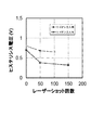
- FIG. 3 is a graph in which the hysteresis voltage near the threshold voltage obtained from the transfer characteristics (the gate voltage dependence of the drain current) of the TFT prepared in the above-described process example is plotted against the number of shots of XeF laser annealing. It is.
- FIG. 3 shows the case without Si ion implantation and the case without Si ion implantation.
- the hysteresis voltage (V) on the vertical axis of the graph is the difference between the voltage characteristic when the gate voltage is swept from negative to positive and the voltage characteristic obtained by sweeping from positive to negative. It was evaluated as the difference in threshold voltage obtained from the characteristics.
- the oxide semiconductor device and the manufacturing method thereof according to the embodiment of the present invention it is possible to improve the stability when stress is applied and to improve the durability in outdoor use or long-time use. Can be made.
- a device having high stability can be obtained by adding laser annealing to the active layer region.
- TFT TFT
- 10 glass substrate
- 11 gate terminal
- 12 gate insulating film
- 13 channel layer
- 14 source terminal
- 15 drain terminal
- 16 Passivation film
Landscapes
- Thin Film Transistor (AREA)
Abstract
酸化物半導体で構成された活性層領域を備える酸化物半導体装置において、ストレス印加時の安定性を向上させる。 酸化物半導体装置は、インジウム(In),ガリウム(Ga),亜鉛(Zn)の酸化物半導体で構成された活性層領域を備え、この活性層領域に、第4族元素のチタン(Ti),ジルコニウム(Zr),ハフニウム(Hf)又は第14族元素の炭素(C),ケイ素(Si),ゲルマニウム(Ge),スズ(Sn)から選択される元素を、数密度で1×10¹⁶~1×1020cm-3の範囲内で含有させた。
Description
本発明は、酸化物半導体装置及びその製造方法に関するものである。
TFT(Thin Film Transistor)は、ガラス基板上に形成されるフラットパネルディスプレイ用のアクティブ素子として普及している。TFTは、基本構成として、ゲート端子、ソース端子及びドレイン端子を備えた3端子素子であり、基板上に成膜した半導体薄膜を、電子又はホールが移動するチャネル層として用い、ゲート端子に電圧を印加して、チャネル層に流れる電流を制御し、ソース端子とドレイン端子間の電流をスイッチングする機能を有する。
TFTのチャネル層としては、多結晶シリコン薄膜やアモルファスシリコン薄膜が広く用いられているが、スマートフォンに代表されるモバイル電子機器の普及によって、小型画面のディスプレイに超高精細・高画質且つ低消費電力の画像表示性能が求められており、これに対応できるTFT材料として、酸化物半導体が注目されている。
酸化物半導体の中で、インジウム(In),ガリウム(Ga),亜鉛(Zn)の酸化物であるIGZOは、従来のアモルファスシリコンなどに比べて、ディスプレイの高精細化や低消費電力化が可能になるTFT材料であることが知られている。下記特許文献1には、気相成膜法で成膜され、In、Ga、Zn及びOの元素から構成される透明アモルファス酸化物薄膜であって、酸化物の組成は、結晶化したときの組成がInGaO3(ZnO)m(mは6未満の自然数)であり、不純物イオンを添加することなしに、電子移動度が1cm2/(V・秒)超、かつ電子キャリヤ濃度が1016/cm3以下である半絶縁性である透明半絶縁性アモルファス酸化物薄膜をTFTのチャネル層とすることが示されている。
前述したように、IGZOは、ディスプレイ用TFTのチャネル材料として有効であるが、酸素欠損に起因する欠陥によるTFT特性、特に、しきい値電圧のストレス印加時における安定性には改善の余地がある。特に、モバイル電子機器は、屋外での使用が前提となるため、太陽光照射や温度上昇といったストレスを受けやすい使用状況への対応が求められ、また、長時間の連続動作によって、バックライトによる光ストレスの蓄積が問題になる。
本発明は、このような問題に対処するために提案されたものである。すなわち、本発明は、酸化物半導体の活性層領域を備える酸化物半導体装置において、ストレス印加時の安定性を向上させることを課題としている。
このような課題を解決するために、本発明による酸化物半導体装置は、以下の構成を具備するものである。
インジウム(In),ガリウム(Ga),亜鉛(Zn)の酸化物半導体の活性層領域を備える酸化物半導体装置であって、第4族元素のチタン(Ti),ジルコニウム(Zr),ハフニウム(Hf)又は第14族元素の炭素(C),ケイ素(Si),ゲルマニウム(Ge),スズ(Sn)から選択される元素を、数密度で1×10¹⁶~1×1020cm-3の範囲内で含有させた前記活性層領域を備えることを特徴とする酸化物半導体装置。
インジウム(In),ガリウム(Ga),亜鉛(Zn)の酸化物半導体の活性層領域を備える酸化物半導体装置であって、第4族元素のチタン(Ti),ジルコニウム(Zr),ハフニウム(Hf)又は第14族元素の炭素(C),ケイ素(Si),ゲルマニウム(Ge),スズ(Sn)から選択される元素を、数密度で1×10¹⁶~1×1020cm-3の範囲内で含有させた前記活性層領域を備えることを特徴とする酸化物半導体装置。
以下、図面を参照して本発明の実施形態を説明する。図1は、本発明の実施形態に係る酸化物半導体装置であるTFTの構成例を示している。TFT1は、ガラス基板10上にゲート端子11が形成され、そのケート端子11を覆うようにゲート絶縁膜12が形成され、ゲート絶縁膜12上に、チャネル層13と、チャネル層に接触するソース端子14とドレイン端子15が形成されている。また、チャネル層13とソース端子14とドレイン端子15を覆うように、パッシベーション膜16が形成されている。
各端子の材料は、例えば、ゲート端子11,ソース端子14,ドレイン端子15がTiNで構成され、ゲート絶縁膜12及びパッシベーション膜16がSiO2で構成されている。そして、活性層領域であるチャネル層13は、後述するように、特定元素を注入したIn,Ga,Znの酸化物半導体(IGZO)で構成されている。このTFT1は、ゲート端子11に電圧を印加して、チャネル層13に流れる電流を制御し、ソース端子14とドレイン端子15間の電流をスイッチングする機能を有する。
チャネル層13に注入される元素は、第4族元素であるTi,Zr,Hf、或いは第14族元素であるC,Si,Ge,Snである。以下、Siを注入する場合を例にして説明するが、前述した各元素であれば同等の効果を得ることができる。ここでの元素注入量は、酸化物半導体に、バルク材以外の材料を不純物として機能する程度の量だけ注入するものであり、これによって、酸素欠損に起因する欠陥によるTFT特性、特に、しきい値電圧の安定性を改善することができる。好ましい元素注入量は、数密度で1×10¹⁶~1×1020cm-3の範囲である。
以下、図1に示した構成のTFT1を得る具体的な工程例(第1実施例)を示す。先ず、ガラス基板10上にスパッタリングでTiNを150nm程度成膜し、フォトリソグラフィーとエッチングでパターニングすることで、ゲート端子11を形成する。ゲート端子11の材料は、TiNに限らず、Al,Ti,Mo,Wなどであってもよい。
次に、プラズマCVD(ガスSiH4,O2,Ar)でSiO2を成膜し、ゲート絶縁膜12を形成する。ゲート絶縁膜12の材料は、SiO2に限らず、シリコン窒化膜や、Al2O3などであってもよい。
その後、IGZO(In:Ga:Zn=1:1:1)のターゲットを用い、スパッタリングによりチャネル層13を成膜する。成膜条件の一例としては、膜厚を50nmに設定し、Ar/O2雰囲気で、圧力5mTorr、O2分圧を16%とした。ここでの成膜には、例えば、回転マグネットスパッタ装置を用いることができる。チャネル層13におけるIGZOの元素比率は、前述した比率(In:Ga:Zn=1:1:1)に限定されない。
なお、前述したO2分圧16%は、その後行う水蒸気雰囲気の400℃アニールで、酸素欠損量が1×1017cm-3以下になる条件である。一方、元素注入を行わない従来のIGZO膜(チャネル層)では、O2分圧2%で成膜している。この場合、400℃のアニール後の酸素欠損量は、1×1018cm-3程度になる。
前述した成膜の後、IGZOのチャネル層13に、Siをイオン注入機を用いて注入する。注入条件は、一例として、Si+イオンをエネルギー40keVでドーズ量1×1013cm-2とした。これにより、Si原子が1×1018cm-3の密度でIGZO膜に注入された。Si原子のIGZO中の密度は、1×10¹⁶~1×1020cm-3、好ましくは、1×10¹⁷~1×1019cm-3とする。
Siの注入後、水分雰囲気(H2O/O2=100/900sccm)、400℃で1時間アニールを行う。アニール温度は、400℃に限らず、300℃~800℃、好ましくは、350℃~500℃である。また、ここでのアニールは、水分雰囲気に限らず、酸素雰囲気であってもよい。
Siが注入されたIGZO膜は、前述したアニールの後、フォトリソグラフィーとエッチングでパターニングして、島状のチャネル層13を形成する。
その後は、ソース端子14とドレイン端子15となるTiNを、例えば150nm成膜し、フォトリソグラフィーとエッチングで、ソース端子14とドレイン端子15とを形成する。ソース端子14とドレイン端子15の材料は、Tiに限らず、Al,Ti,Mo,Wなどであってもよい。その後は、パッシベーション膜16となるSiO2をプラズマCVDなどで成膜し、その後、フォトリソグラフィーとエッチングにより、各端子(ソース端子14,ドレイン端子15,ゲート端子11)への電気的接触が可能なように接続端子を形成する。
このようにして得られたTFT1(図1参照)は、負バイアス・光ストレスの継続的印加に対して、安定したTFT特性を示すことが試験にて確認された。試験条件は、デバイス寸法が、チャネル長:40μm、チャネル幅:20μmであり、ストレス条件として、ゲート電圧に-20Vを印加し、白色LEDによる光照射(30,000lx)を雰囲気温度60℃にて行った。
図2は、前述したストレスを経時的に加えた場合のTFT1のしきい値電圧の変化(ΔVT(V))を示している。図2に示されるように、Siイオンを注入しなかったIGZO膜のチャネル層を備えるTFTに対して、Siイオンを注入したIGZO膜のチャネル層13を備えるTFT1の方が、しきい値電圧の経時的変化(ΔVT(V))が少ないことが確認できる。
このような試験結果は、活性層領域のIGZO膜にSiを所定量注入することにより、TFT動作の安定性が向上することを示している。このような結果は、酸素欠損に起因するキャリアではなく、Siがドーパントとして働き、キャリアである電子を供給しているためであり、酸素欠損により形成されるIGZOのバンドギャップ内における深い準位のトラップが減少しているからと考えられる。
次に他の工程例(第2実施例)を説明する。この例では、前述した工程例(第1実施例)における水分雰囲気のアニールの前に、波長400nm以下のXeFレーザーによる局所レーザーアニールを行った。他の工程は第1実施例と同様である。
レーザーアニールにおけるレーザーエネルギー密度は、一回の照射で150mJ/cm2とし、これを重畳させることでアニールを行った。アニールした領域は、60μm×60μmとし、TFTのチャネル層13となる活性層領域が含まれるようにアニールした。レーザー照射の位置合わせには、ゲート端子11のパターンを用いた。なお、トップゲートTFTを作成する場合には、ゲート端子11を位置合わせに用いることができないが、何らかの位置合わせパターンを自在に形成しておくことで、局所レーザーアニールを活性層領域に精度良く実施することが可能になる。
図3は、前述の工程例で作成したTFTの伝達特性(ドレイン電流のゲート電圧依存性)から求めた、しきい値電圧付近のヒステリシス電圧を、XeFレーザーアニールのshot回数に対してプロットしたグラフである。図3においては、Siイオン注入無しの場合とSiイオン注入無しの場合を示している。
グラフ縦軸のヒステリシス電圧(V)は、ゲート電圧を負から正に掃引した場合の電圧特性と、正から負に掃引して求めた電圧特性のずれであり、具体的には、両者の電圧特性から求めたしきい値電圧の差として評価した。
図3から明らかなように、XeFレーザーの局所アニールを導入することで、IGZOを活性層領域に用いたTFTのヒステリシス電圧が低減し、TFTの安定性が向上することが確認できた。IGZO膜中に例えば電子を捕獲するようなトラップ準位があると、ヒステリシス電圧は増加し、不安定なデバイスとなってしまうが、IGZOの活性層領域にSiを注入してレーザーアニールを行うことで、電子を捕獲するようなトラップ準位が少なくなると考えられる。
以上説明したように、本発明の実施形態に係る酸化物半導体装置及びその製造方法によると、ストレス印加時の安定性を向上させることができ、屋外使用や長時間使用などでの耐久性を向上させることができる。また、活性層領域へのレーザーアニールを追加することで、安定性の高いデバイスを得ることができる。
1:TFT,10:ガラス基板,11:ゲート端子,12:ゲート絶縁膜,
13:チャネル層,14:ソース端子,15:ドレイン端子,
16:パッシベーション膜
13:チャネル層,14:ソース端子,15:ドレイン端子,
16:パッシベーション膜
Claims (3)
- インジウム(In),ガリウム(Ga),亜鉛(Zn)の酸化物半導体で構成される活性層領域を有する酸化物半導体装置であって、第4族元素のチタン(Ti),ジルコニウム(Zr),ハフニウム(Hf)又は第14族元素の炭素(C),ケイ素(Si),ゲルマニウム(Ge),スズ(Sn)から選択される元素を、数密度で1×10¹⁶~1×1020cm-3の範囲内で含有させた前記活性層領域を備えることを特徴とする酸化物半導体装置。
- 前記活性層領域は、波長400nm以下のレーザーを照射してアニールした領域であることを特徴とする請求項1記載の酸化物半導体装置。
- インジウム(In),ガリウム(Ga),亜鉛(Zn)の酸化物半導体で構成される活性層領域を有する酸化物半導体装置の製造方法であって、
前記活性層領域に、第4族元素のチタン(Ti),ジルコニウム(Zr),ハフニウム(Hf)又は第14族元素の炭素(C),ケイ素(Si),ゲルマニウム(Ge),スズ(Sn)から選択される元素を、数密度で1×10¹⁶~1×1020cm-3の範囲内イオン注入する工程と、
イオン注入後の前記活性層領域に、波長400nm以下のレーザーを照射して、アニールする工程とを有することを特徴とする酸化物半導体の製造方法。
Priority Applications (3)
| Application Number | Priority Date | Filing Date | Title |
|---|---|---|---|
| CN201780056959.9A CN109716532A (zh) | 2016-10-21 | 2017-09-04 | 氧化物半导体装置及其制造方法 |
| US16/343,022 US10896978B2 (en) | 2016-10-21 | 2017-09-04 | Oxide semiconductor device and method for manufacturing same |
| KR1020197007621A KR20190062397A (ko) | 2016-10-21 | 2017-09-04 | 산화물 반도체 장치 및 그 제조 방법 |
Applications Claiming Priority (2)
| Application Number | Priority Date | Filing Date | Title |
|---|---|---|---|
| JP2016-206647 | 2016-10-21 | ||
| JP2016206647A JP2018067672A (ja) | 2016-10-21 | 2016-10-21 | 酸化物半導体装置及びその製造方法 |
Publications (1)
| Publication Number | Publication Date |
|---|---|
| WO2018074083A1 true WO2018074083A1 (ja) | 2018-04-26 |
Family
ID=62019070
Family Applications (1)
| Application Number | Title | Priority Date | Filing Date |
|---|---|---|---|
| PCT/JP2017/031817 Ceased WO2018074083A1 (ja) | 2016-10-21 | 2017-09-04 | 酸化物半導体装置及びその製造方法 |
Country Status (6)
| Country | Link |
|---|---|
| US (1) | US10896978B2 (ja) |
| JP (1) | JP2018067672A (ja) |
| KR (1) | KR20190062397A (ja) |
| CN (1) | CN109716532A (ja) |
| TW (1) | TW201820423A (ja) |
| WO (1) | WO2018074083A1 (ja) |
Cited By (2)
| Publication number | Priority date | Publication date | Assignee | Title |
|---|---|---|---|---|
| WO2019244945A1 (ja) * | 2018-06-21 | 2019-12-26 | 株式会社アルバック | 酸化物半導体薄膜、薄膜トランジスタおよびその製造方法、ならびにスパッタリングターゲット |
| WO2020261748A1 (ja) * | 2019-06-28 | 2020-12-30 | 株式会社アルバック | スパッタリングターゲット及びスパッタリングターゲットの製造方法 |
Families Citing this family (3)
| Publication number | Priority date | Publication date | Assignee | Title |
|---|---|---|---|---|
| CN112119500B (zh) * | 2018-05-21 | 2025-06-17 | 索尼公司 | 固态摄像元件及其制造方法 |
| JP7230743B2 (ja) * | 2019-08-27 | 2023-03-01 | 株式会社デンソー | 半導体装置の製造方法 |
| US11430898B2 (en) * | 2020-03-13 | 2022-08-30 | Applied Materials, Inc. | Oxygen vacancy of amorphous indium gallium zinc oxide passivation by silicon ion treatment |
Citations (4)
| Publication number | Priority date | Publication date | Assignee | Title |
|---|---|---|---|---|
| JP2011101027A (ja) * | 2009-03-31 | 2011-05-19 | Panasonic Corp | フレキシブル半導体装置およびその製造方法 |
| JP2012028481A (ja) * | 2010-07-22 | 2012-02-09 | Fujifilm Corp | 電界効果型トランジスタ及びその製造方法 |
| JP2013110176A (ja) * | 2011-11-18 | 2013-06-06 | Semiconductor Energy Lab Co Ltd | 半導体装置および半導体装置の作製方法 |
| JP2015228495A (ja) * | 2014-05-08 | 2015-12-17 | 株式会社Flosfia | 結晶性積層構造体、半導体装置 |
Family Cites Families (5)
| Publication number | Priority date | Publication date | Assignee | Title |
|---|---|---|---|---|
| EP2413366B1 (en) | 2004-03-12 | 2017-01-11 | Japan Science And Technology Agency | A switching element of LCDs or organic EL displays |
| CN102163625A (zh) * | 2011-03-17 | 2011-08-24 | 复旦大学 | 用于氧化物薄膜晶体管的半导体层材料铟锌钛氧化物 |
| JP4982620B1 (ja) * | 2011-07-29 | 2012-07-25 | 富士フイルム株式会社 | 電界効果型トランジスタの製造方法、並びに、電界効果型トランジスタ、表示装置、イメージセンサ及びx線センサ |
| JP5052693B1 (ja) * | 2011-08-12 | 2012-10-17 | 富士フイルム株式会社 | 薄膜トランジスタ及びその製造方法、表示装置、イメージセンサー、x線センサー並びにx線デジタル撮影装置 |
| CN106415845B (zh) * | 2014-07-22 | 2019-12-10 | 株式会社Flosfia | 结晶性半导体膜和板状体以及半导体装置 |
-
2016
- 2016-10-21 JP JP2016206647A patent/JP2018067672A/ja active Pending
-
2017
- 2017-09-04 US US16/343,022 patent/US10896978B2/en not_active Expired - Fee Related
- 2017-09-04 KR KR1020197007621A patent/KR20190062397A/ko not_active Ceased
- 2017-09-04 CN CN201780056959.9A patent/CN109716532A/zh active Pending
- 2017-09-04 WO PCT/JP2017/031817 patent/WO2018074083A1/ja not_active Ceased
- 2017-10-16 TW TW106135273A patent/TW201820423A/zh unknown
Patent Citations (4)
| Publication number | Priority date | Publication date | Assignee | Title |
|---|---|---|---|---|
| JP2011101027A (ja) * | 2009-03-31 | 2011-05-19 | Panasonic Corp | フレキシブル半導体装置およびその製造方法 |
| JP2012028481A (ja) * | 2010-07-22 | 2012-02-09 | Fujifilm Corp | 電界効果型トランジスタ及びその製造方法 |
| JP2013110176A (ja) * | 2011-11-18 | 2013-06-06 | Semiconductor Energy Lab Co Ltd | 半導体装置および半導体装置の作製方法 |
| JP2015228495A (ja) * | 2014-05-08 | 2015-12-17 | 株式会社Flosfia | 結晶性積層構造体、半導体装置 |
Cited By (9)
| Publication number | Priority date | Publication date | Assignee | Title |
|---|---|---|---|---|
| WO2019244945A1 (ja) * | 2018-06-21 | 2019-12-26 | 株式会社アルバック | 酸化物半導体薄膜、薄膜トランジスタおよびその製造方法、ならびにスパッタリングターゲット |
| JPWO2019244945A1 (ja) * | 2018-06-21 | 2020-06-25 | 株式会社アルバック | 酸化物半導体薄膜、薄膜トランジスタおよびその製造方法、ならびにスパッタリングターゲット |
| US11335782B2 (en) | 2018-06-21 | 2022-05-17 | Ulvac, Inc. | Oxide semiconductor thin film, thin film transistor, method producing the same, and sputtering target |
| WO2020261748A1 (ja) * | 2019-06-28 | 2020-12-30 | 株式会社アルバック | スパッタリングターゲット及びスパッタリングターゲットの製造方法 |
| JPWO2020261748A1 (ja) * | 2019-06-28 | 2021-09-13 | 株式会社アルバック | スパッタリングターゲット及びスパッタリングターゲットの製造方法 |
| KR20220009453A (ko) * | 2019-06-28 | 2022-01-24 | 가부시키가이샤 아루박 | 스퍼터링 타깃 및 스퍼터링 타깃의 제조방법 |
| JP7128284B2 (ja) | 2019-06-28 | 2022-08-30 | 株式会社アルバック | スパッタリングターゲットの製造方法 |
| US12012650B2 (en) | 2019-06-28 | 2024-06-18 | Ulvac, Inc. | Sputtering target and method of producing sputtering target |
| KR102747438B1 (ko) | 2019-06-28 | 2024-12-26 | 가부시키가이샤 아루박 | 스퍼터링 타깃 및 스퍼터링 타깃의 제조방법 |
Also Published As
| Publication number | Publication date |
|---|---|
| JP2018067672A (ja) | 2018-04-26 |
| CN109716532A (zh) | 2019-05-03 |
| KR20190062397A (ko) | 2019-06-05 |
| US10896978B2 (en) | 2021-01-19 |
| US20190288115A1 (en) | 2019-09-19 |
| TW201820423A (zh) | 2018-06-01 |
Similar Documents
| Publication | Publication Date | Title |
|---|---|---|
| US8101949B2 (en) | Treatment of gate dielectric for making high performance metal oxide and metal oxynitride thin film transistors | |
| US11011534B2 (en) | Multi-level cell thin-film transistor memory and method of fabricating the same | |
| JP2008199005A (ja) | 薄膜トランジスタ及びその製造方法 | |
| JP2018067672A (ja) | 酸化物半導体装置及びその製造方法 | |
| US9773921B2 (en) | Combo amorphous and LTPS transistors | |
| CN104752516A (zh) | 氧化物半导体薄膜晶体管及其制造方法 | |
| Liang et al. | Effects of interface trap density on the electrical performance of amorphous InSnZnO thin-film transistor | |
| Tsai et al. | Positive Gate-Bias Temperature Stability of RF-Sputtered $\hbox {Mg} _ {0.05}\hbox {Zn} _ {0.95}\hbox {O} $ Active-Layer Thin-Film Transistors | |
| CN107104151A (zh) | 一种双栅电极金属氧化物薄膜晶体管及其制备方法 | |
| KR102431926B1 (ko) | 산화물 박막 트랜지스터 | |
| KR102231372B1 (ko) | 산화물 반도체 박막 트랜지스터 및 이의 제조방법 | |
| KR101488623B1 (ko) | 산화물 박막 트랜지스터 제조방법 | |
| TW201946874A (zh) | 含有氧化物半導體層的薄膜電晶體 | |
| Kang et al. | Improvement of on/off current ratio of amorphous In–Ga–Zn–O thin-film transistor with off-planed source/drain electrodes | |
| KR101088366B1 (ko) | 매설층을 갖는 박막 트랜지스터 및 그 제조 방법 | |
| Zhan et al. | P. 18: Effects of Interface and Bulk States on the Stability of Amorphous InGaZnO Thin Film Transistors under Gate Bias and Temperature Stress | |
| Jiang et al. | P‐1.5: The effects of the temperature of fluorination treatment on the reliability of an indium‐gallium‐zinc oxide thin‐film transistor | |
| KR101669723B1 (ko) | 게르마늄이 도핑된 InZnO 활성층을 적용한 박막 트랜지스터 및 이의 제조방법 | |
| KR102431925B1 (ko) | 전기적 성능을 개선하기 위한 펨토초 레이저 공정을 이용한 tft 제작 방법 | |
| KR102431922B1 (ko) | 펨토초 레이저를 이용한 트랜지스터 제작 방법 | |
| US20190326421A1 (en) | Method for manufacturing oxide semiconductor device | |
| CN108091572A (zh) | 薄膜晶体管的制作方法及薄膜晶体管 | |
| CN110349972A (zh) | 一种薄膜晶体管基板及其制备方法 | |
| Wong et al. | Elevated‐Metal Metal‐Oxide Thin‐Film Transistors: A Back‐Gate Transistor Architecture with Annealing‐Induced Source/Drain Regions | |
| KR101303428B1 (ko) | 산화물 박막트랜지스터 소자 및 그의 제조방법 |
Legal Events
| Date | Code | Title | Description |
|---|---|---|---|
| 121 | Ep: the epo has been informed by wipo that ep was designated in this application |
Ref document number: 17862487 Country of ref document: EP Kind code of ref document: A1 |
|
| ENP | Entry into the national phase |
Ref document number: 20197007621 Country of ref document: KR Kind code of ref document: A |
|
| NENP | Non-entry into the national phase |
Ref country code: DE |
|
| 122 | Ep: pct application non-entry in european phase |
Ref document number: 17862487 Country of ref document: EP Kind code of ref document: A1 |