WO2018066420A1 - 半導体装置 - Google Patents
半導体装置 Download PDFInfo
- Publication number
- WO2018066420A1 WO2018066420A1 PCT/JP2017/034829 JP2017034829W WO2018066420A1 WO 2018066420 A1 WO2018066420 A1 WO 2018066420A1 JP 2017034829 W JP2017034829 W JP 2017034829W WO 2018066420 A1 WO2018066420 A1 WO 2018066420A1
- Authority
- WO
- WIPO (PCT)
- Prior art keywords
- chip
- lead
- switching element
- current path
- semiconductor device
- Prior art date
- Legal status (The legal status is an assumption and is not a legal conclusion. Google has not performed a legal analysis and makes no representation as to the accuracy of the status listed.)
- Ceased
Links
Images

Classifications
-
- G—PHYSICS
- G01—MEASURING; TESTING
- G01R—MEASURING ELECTRIC VARIABLES; MEASURING MAGNETIC VARIABLES
- G01R1/00—Details of instruments or arrangements of the types included in groups G01R5/00 - G01R13/00 and G01R31/00
- G01R1/20—Modifications of basic electric elements for use in electric measuring instruments; Structural combinations of such elements with such instruments
- G01R1/203—Resistors used for electric measuring, e.g. decade resistors standards, resistors for comparators, series resistors, shunts
-
- G—PHYSICS
- G01—MEASURING; TESTING
- G01R—MEASURING ELECTRIC VARIABLES; MEASURING MAGNETIC VARIABLES
- G01R15/00—Details of measuring arrangements of the types provided for in groups G01R17/00 - G01R29/00, G01R33/00 - G01R33/26 or G01R35/00
- G01R15/14—Adaptations providing voltage or current isolation, e.g. for high-voltage or high-current networks
- G01R15/146—Measuring arrangements for current not covered by other subgroups of G01R15/14, e.g. using current dividers, shunts, or measuring a voltage drop
-
- G—PHYSICS
- G01—MEASURING; TESTING
- G01R—MEASURING ELECTRIC VARIABLES; MEASURING MAGNETIC VARIABLES
- G01R19/00—Arrangements for measuring currents or voltages or for indicating presence or sign thereof
- G01R19/0092—Arrangements for measuring currents or voltages or for indicating presence or sign thereof measuring current only
-
- H—ELECTRICITY
- H01—ELECTRIC ELEMENTS
- H01L—SEMICONDUCTOR DEVICES NOT COVERED BY CLASS H10
- H01L23/00—Details of semiconductor or other solid state devices
- H01L23/28—Encapsulations, e.g. encapsulating layers, coatings, e.g. for protection
- H01L23/31—Encapsulations, e.g. encapsulating layers, coatings, e.g. for protection characterised by the arrangement or shape
- H01L23/3107—Encapsulations, e.g. encapsulating layers, coatings, e.g. for protection characterised by the arrangement or shape the device being completely enclosed
- H01L23/3121—Encapsulations, e.g. encapsulating layers, coatings, e.g. for protection characterised by the arrangement or shape the device being completely enclosed a substrate forming part of the encapsulation
-
- H—ELECTRICITY
- H01—ELECTRIC ELEMENTS
- H01L—SEMICONDUCTOR DEVICES NOT COVERED BY CLASS H10
- H01L23/00—Details of semiconductor or other solid state devices
- H01L23/34—Arrangements for cooling, heating, ventilating or temperature compensation ; Temperature sensing arrangements
- H01L23/40—Mountings or securing means for detachable cooling or heating arrangements ; fixed by friction, plugs or springs
- H01L23/4006—Mountings or securing means for detachable cooling or heating arrangements ; fixed by friction, plugs or springs with bolts or screws
-
- H—ELECTRICITY
- H01—ELECTRIC ELEMENTS
- H01L—SEMICONDUCTOR DEVICES NOT COVERED BY CLASS H10
- H01L23/00—Details of semiconductor or other solid state devices
- H01L23/48—Arrangements for conducting electric current to or from the solid state body in operation, e.g. leads, terminal arrangements ; Selection of materials therefor
- H01L23/488—Arrangements for conducting electric current to or from the solid state body in operation, e.g. leads, terminal arrangements ; Selection of materials therefor consisting of soldered or bonded constructions
- H01L23/495—Lead-frames or other flat leads
- H01L23/49517—Additional leads
- H01L23/49524—Additional leads the additional leads being a tape carrier or flat leads
-
- H—ELECTRICITY
- H01—ELECTRIC ELEMENTS
- H01L—SEMICONDUCTOR DEVICES NOT COVERED BY CLASS H10
- H01L23/00—Details of semiconductor or other solid state devices
- H01L23/48—Arrangements for conducting electric current to or from the solid state body in operation, e.g. leads, terminal arrangements ; Selection of materials therefor
- H01L23/488—Arrangements for conducting electric current to or from the solid state body in operation, e.g. leads, terminal arrangements ; Selection of materials therefor consisting of soldered or bonded constructions
- H01L23/495—Lead-frames or other flat leads
- H01L23/49541—Geometry of the lead-frame
- H01L23/49562—Geometry of the lead-frame for individual devices of subclass H10D
-
- H—ELECTRICITY
- H01—ELECTRIC ELEMENTS
- H01L—SEMICONDUCTOR DEVICES NOT COVERED BY CLASS H10
- H01L23/00—Details of semiconductor or other solid state devices
- H01L23/48—Arrangements for conducting electric current to or from the solid state body in operation, e.g. leads, terminal arrangements ; Selection of materials therefor
- H01L23/488—Arrangements for conducting electric current to or from the solid state body in operation, e.g. leads, terminal arrangements ; Selection of materials therefor consisting of soldered or bonded constructions
- H01L23/495—Lead-frames or other flat leads
- H01L23/49575—Assemblies of semiconductor devices on lead frames
-
- H—ELECTRICITY
- H01—ELECTRIC ELEMENTS
- H01L—SEMICONDUCTOR DEVICES NOT COVERED BY CLASS H10
- H01L24/00—Arrangements for connecting or disconnecting semiconductor or solid-state bodies; Methods or apparatus related thereto
- H01L24/01—Means for bonding being attached to, or being formed on, the surface to be connected, e.g. chip-to-package, die-attach, "first-level" interconnects; Manufacturing methods related thereto
- H01L24/42—Wire connectors; Manufacturing methods related thereto
- H01L24/47—Structure, shape, material or disposition of the wire connectors after the connecting process
- H01L24/48—Structure, shape, material or disposition of the wire connectors after the connecting process of an individual wire connector
-
- H—ELECTRICITY
- H01—ELECTRIC ELEMENTS
- H01L—SEMICONDUCTOR DEVICES NOT COVERED BY CLASS H10
- H01L25/00—Assemblies consisting of a plurality of semiconductor or other solid state devices
- H01L25/03—Assemblies consisting of a plurality of semiconductor or other solid state devices all the devices being of a type provided for in a single subclass of subclasses H10B, H10D, H10F, H10H, H10K or H10N, e.g. assemblies of rectifier diodes
- H01L25/04—Assemblies consisting of a plurality of semiconductor or other solid state devices all the devices being of a type provided for in a single subclass of subclasses H10B, H10D, H10F, H10H, H10K or H10N, e.g. assemblies of rectifier diodes the devices not having separate containers
- H01L25/07—Assemblies consisting of a plurality of semiconductor or other solid state devices all the devices being of a type provided for in a single subclass of subclasses H10B, H10D, H10F, H10H, H10K or H10N, e.g. assemblies of rectifier diodes the devices not having separate containers the devices being of a type provided for in group subclass H10D
- H01L25/072—Assemblies consisting of a plurality of semiconductor or other solid state devices all the devices being of a type provided for in a single subclass of subclasses H10B, H10D, H10F, H10H, H10K or H10N, e.g. assemblies of rectifier diodes the devices not having separate containers the devices being of a type provided for in group subclass H10D the devices being arranged next to each other
-
- H—ELECTRICITY
- H01—ELECTRIC ELEMENTS
- H01L—SEMICONDUCTOR DEVICES NOT COVERED BY CLASS H10
- H01L25/00—Assemblies consisting of a plurality of semiconductor or other solid state devices
- H01L25/18—Assemblies consisting of a plurality of semiconductor or other solid state devices the devices being of the types provided for in two or more different main groups of the same subclass of H10B, H10D, H10F, H10H, H10K or H10N
-
- H—ELECTRICITY
- H01—ELECTRIC ELEMENTS
- H01L—SEMICONDUCTOR DEVICES NOT COVERED BY CLASS H10
- H01L23/00—Details of semiconductor or other solid state devices
- H01L23/34—Arrangements for cooling, heating, ventilating or temperature compensation ; Temperature sensing arrangements
- H01L23/40—Mountings or securing means for detachable cooling or heating arrangements ; fixed by friction, plugs or springs
- H01L23/4006—Mountings or securing means for detachable cooling or heating arrangements ; fixed by friction, plugs or springs with bolts or screws
- H01L2023/4018—Mountings or securing means for detachable cooling or heating arrangements ; fixed by friction, plugs or springs with bolts or screws characterised by the type of device to be heated or cooled
- H01L2023/4031—Packaged discrete devices, e.g. to-3 housings, diodes
-
- H—ELECTRICITY
- H01—ELECTRIC ELEMENTS
- H01L—SEMICONDUCTOR DEVICES NOT COVERED BY CLASS H10
- H01L23/00—Details of semiconductor or other solid state devices
- H01L23/34—Arrangements for cooling, heating, ventilating or temperature compensation ; Temperature sensing arrangements
- H01L23/40—Mountings or securing means for detachable cooling or heating arrangements ; fixed by friction, plugs or springs
- H01L23/4006—Mountings or securing means for detachable cooling or heating arrangements ; fixed by friction, plugs or springs with bolts or screws
- H01L2023/4075—Mechanical elements
- H01L2023/4087—Mounting accessories, interposers, clamping or screwing parts
-
- H—ELECTRICITY
- H01—ELECTRIC ELEMENTS
- H01L—SEMICONDUCTOR DEVICES NOT COVERED BY CLASS H10
- H01L2224/00—Indexing scheme for arrangements for connecting or disconnecting semiconductor or solid-state bodies and methods related thereto as covered by H01L24/00
- H01L2224/01—Means for bonding being attached to, or being formed on, the surface to be connected, e.g. chip-to-package, die-attach, "first-level" interconnects; Manufacturing methods related thereto
- H01L2224/02—Bonding areas; Manufacturing methods related thereto
- H01L2224/04—Structure, shape, material or disposition of the bonding areas prior to the connecting process
- H01L2224/04034—Bonding areas specifically adapted for strap connectors
-
- H—ELECTRICITY
- H01—ELECTRIC ELEMENTS
- H01L—SEMICONDUCTOR DEVICES NOT COVERED BY CLASS H10
- H01L2224/00—Indexing scheme for arrangements for connecting or disconnecting semiconductor or solid-state bodies and methods related thereto as covered by H01L24/00
- H01L2224/01—Means for bonding being attached to, or being formed on, the surface to be connected, e.g. chip-to-package, die-attach, "first-level" interconnects; Manufacturing methods related thereto
- H01L2224/02—Bonding areas; Manufacturing methods related thereto
- H01L2224/04—Structure, shape, material or disposition of the bonding areas prior to the connecting process
- H01L2224/04042—Bonding areas specifically adapted for wire connectors, e.g. wirebond pads
-
- H—ELECTRICITY
- H01—ELECTRIC ELEMENTS
- H01L—SEMICONDUCTOR DEVICES NOT COVERED BY CLASS H10
- H01L2224/00—Indexing scheme for arrangements for connecting or disconnecting semiconductor or solid-state bodies and methods related thereto as covered by H01L24/00
- H01L2224/01—Means for bonding being attached to, or being formed on, the surface to be connected, e.g. chip-to-package, die-attach, "first-level" interconnects; Manufacturing methods related thereto
- H01L2224/02—Bonding areas; Manufacturing methods related thereto
- H01L2224/04—Structure, shape, material or disposition of the bonding areas prior to the connecting process
- H01L2224/05—Structure, shape, material or disposition of the bonding areas prior to the connecting process of an individual bonding area
- H01L2224/0554—External layer
- H01L2224/05599—Material
-
- H—ELECTRICITY
- H01—ELECTRIC ELEMENTS
- H01L—SEMICONDUCTOR DEVICES NOT COVERED BY CLASS H10
- H01L2224/00—Indexing scheme for arrangements for connecting or disconnecting semiconductor or solid-state bodies and methods related thereto as covered by H01L24/00
- H01L2224/01—Means for bonding being attached to, or being formed on, the surface to be connected, e.g. chip-to-package, die-attach, "first-level" interconnects; Manufacturing methods related thereto
- H01L2224/02—Bonding areas; Manufacturing methods related thereto
- H01L2224/04—Structure, shape, material or disposition of the bonding areas prior to the connecting process
- H01L2224/06—Structure, shape, material or disposition of the bonding areas prior to the connecting process of a plurality of bonding areas
- H01L2224/0601—Structure
- H01L2224/0603—Bonding areas having different sizes, e.g. different heights or widths
-
- H—ELECTRICITY
- H01—ELECTRIC ELEMENTS
- H01L—SEMICONDUCTOR DEVICES NOT COVERED BY CLASS H10
- H01L2224/00—Indexing scheme for arrangements for connecting or disconnecting semiconductor or solid-state bodies and methods related thereto as covered by H01L24/00
- H01L2224/01—Means for bonding being attached to, or being formed on, the surface to be connected, e.g. chip-to-package, die-attach, "first-level" interconnects; Manufacturing methods related thereto
- H01L2224/02—Bonding areas; Manufacturing methods related thereto
- H01L2224/04—Structure, shape, material or disposition of the bonding areas prior to the connecting process
- H01L2224/06—Structure, shape, material or disposition of the bonding areas prior to the connecting process of a plurality of bonding areas
- H01L2224/061—Disposition
- H01L2224/0618—Disposition being disposed on at least two different sides of the body, e.g. dual array
- H01L2224/06181—On opposite sides of the body
-
- H—ELECTRICITY
- H01—ELECTRIC ELEMENTS
- H01L—SEMICONDUCTOR DEVICES NOT COVERED BY CLASS H10
- H01L2224/00—Indexing scheme for arrangements for connecting or disconnecting semiconductor or solid-state bodies and methods related thereto as covered by H01L24/00
- H01L2224/01—Means for bonding being attached to, or being formed on, the surface to be connected, e.g. chip-to-package, die-attach, "first-level" interconnects; Manufacturing methods related thereto
- H01L2224/26—Layer connectors, e.g. plate connectors, solder or adhesive layers; Manufacturing methods related thereto
- H01L2224/28—Structure, shape, material or disposition of the layer connectors prior to the connecting process
- H01L2224/29—Structure, shape, material or disposition of the layer connectors prior to the connecting process of an individual layer connector
- H01L2224/29001—Core members of the layer connector
- H01L2224/29099—Material
- H01L2224/291—Material with a principal constituent of the material being a metal or a metalloid, e.g. boron [B], silicon [Si], germanium [Ge], arsenic [As], antimony [Sb], tellurium [Te] and polonium [Po], and alloys thereof
-
- H—ELECTRICITY
- H01—ELECTRIC ELEMENTS
- H01L—SEMICONDUCTOR DEVICES NOT COVERED BY CLASS H10
- H01L2224/00—Indexing scheme for arrangements for connecting or disconnecting semiconductor or solid-state bodies and methods related thereto as covered by H01L24/00
- H01L2224/01—Means for bonding being attached to, or being formed on, the surface to be connected, e.g. chip-to-package, die-attach, "first-level" interconnects; Manufacturing methods related thereto
- H01L2224/26—Layer connectors, e.g. plate connectors, solder or adhesive layers; Manufacturing methods related thereto
- H01L2224/31—Structure, shape, material or disposition of the layer connectors after the connecting process
- H01L2224/32—Structure, shape, material or disposition of the layer connectors after the connecting process of an individual layer connector
- H01L2224/321—Disposition
- H01L2224/32151—Disposition the layer connector connecting between a semiconductor or solid-state body and an item not being a semiconductor or solid-state body, e.g. chip-to-substrate, chip-to-passive
- H01L2224/32221—Disposition the layer connector connecting between a semiconductor or solid-state body and an item not being a semiconductor or solid-state body, e.g. chip-to-substrate, chip-to-passive the body and the item being stacked
- H01L2224/32245—Disposition the layer connector connecting between a semiconductor or solid-state body and an item not being a semiconductor or solid-state body, e.g. chip-to-substrate, chip-to-passive the body and the item being stacked the item being metallic
-
- H—ELECTRICITY
- H01—ELECTRIC ELEMENTS
- H01L—SEMICONDUCTOR DEVICES NOT COVERED BY CLASS H10
- H01L2224/00—Indexing scheme for arrangements for connecting or disconnecting semiconductor or solid-state bodies and methods related thereto as covered by H01L24/00
- H01L2224/01—Means for bonding being attached to, or being formed on, the surface to be connected, e.g. chip-to-package, die-attach, "first-level" interconnects; Manufacturing methods related thereto
- H01L2224/34—Strap connectors, e.g. copper straps for grounding power devices; Manufacturing methods related thereto
- H01L2224/36—Structure, shape, material or disposition of the strap connectors prior to the connecting process
- H01L2224/37—Structure, shape, material or disposition of the strap connectors prior to the connecting process of an individual strap connector
- H01L2224/37001—Core members of the connector
- H01L2224/37099—Material
- H01L2224/371—Material with a principal constituent of the material being a metal or a metalloid, e.g. boron [B], silicon [Si], germanium [Ge], arsenic [As], antimony [Sb], tellurium [Te] and polonium [Po], and alloys thereof
- H01L2224/37101—Material with a principal constituent of the material being a metal or a metalloid, e.g. boron [B], silicon [Si], germanium [Ge], arsenic [As], antimony [Sb], tellurium [Te] and polonium [Po], and alloys thereof the principal constituent melting at a temperature of less than 400°C
- H01L2224/37111—Tin [Sn] as principal constituent
-
- H—ELECTRICITY
- H01—ELECTRIC ELEMENTS
- H01L—SEMICONDUCTOR DEVICES NOT COVERED BY CLASS H10
- H01L2224/00—Indexing scheme for arrangements for connecting or disconnecting semiconductor or solid-state bodies and methods related thereto as covered by H01L24/00
- H01L2224/01—Means for bonding being attached to, or being formed on, the surface to be connected, e.g. chip-to-package, die-attach, "first-level" interconnects; Manufacturing methods related thereto
- H01L2224/34—Strap connectors, e.g. copper straps for grounding power devices; Manufacturing methods related thereto
- H01L2224/36—Structure, shape, material or disposition of the strap connectors prior to the connecting process
- H01L2224/37—Structure, shape, material or disposition of the strap connectors prior to the connecting process of an individual strap connector
- H01L2224/37001—Core members of the connector
- H01L2224/37099—Material
- H01L2224/371—Material with a principal constituent of the material being a metal or a metalloid, e.g. boron [B], silicon [Si], germanium [Ge], arsenic [As], antimony [Sb], tellurium [Te] and polonium [Po], and alloys thereof
- H01L2224/37138—Material with a principal constituent of the material being a metal or a metalloid, e.g. boron [B], silicon [Si], germanium [Ge], arsenic [As], antimony [Sb], tellurium [Te] and polonium [Po], and alloys thereof the principal constituent melting at a temperature of greater than or equal to 950°C and less than 1550°C
- H01L2224/37147—Copper [Cu] as principal constituent
-
- H—ELECTRICITY
- H01—ELECTRIC ELEMENTS
- H01L—SEMICONDUCTOR DEVICES NOT COVERED BY CLASS H10
- H01L2224/00—Indexing scheme for arrangements for connecting or disconnecting semiconductor or solid-state bodies and methods related thereto as covered by H01L24/00
- H01L2224/01—Means for bonding being attached to, or being formed on, the surface to be connected, e.g. chip-to-package, die-attach, "first-level" interconnects; Manufacturing methods related thereto
- H01L2224/34—Strap connectors, e.g. copper straps for grounding power devices; Manufacturing methods related thereto
- H01L2224/36—Structure, shape, material or disposition of the strap connectors prior to the connecting process
- H01L2224/37—Structure, shape, material or disposition of the strap connectors prior to the connecting process of an individual strap connector
- H01L2224/37001—Core members of the connector
- H01L2224/37099—Material
- H01L2224/371—Material with a principal constituent of the material being a metal or a metalloid, e.g. boron [B], silicon [Si], germanium [Ge], arsenic [As], antimony [Sb], tellurium [Te] and polonium [Po], and alloys thereof
- H01L2224/37138—Material with a principal constituent of the material being a metal or a metalloid, e.g. boron [B], silicon [Si], germanium [Ge], arsenic [As], antimony [Sb], tellurium [Te] and polonium [Po], and alloys thereof the principal constituent melting at a temperature of greater than or equal to 950°C and less than 1550°C
- H01L2224/37149—Manganese [Mn] as principal constituent
-
- H—ELECTRICITY
- H01—ELECTRIC ELEMENTS
- H01L—SEMICONDUCTOR DEVICES NOT COVERED BY CLASS H10
- H01L2224/00—Indexing scheme for arrangements for connecting or disconnecting semiconductor or solid-state bodies and methods related thereto as covered by H01L24/00
- H01L2224/01—Means for bonding being attached to, or being formed on, the surface to be connected, e.g. chip-to-package, die-attach, "first-level" interconnects; Manufacturing methods related thereto
- H01L2224/34—Strap connectors, e.g. copper straps for grounding power devices; Manufacturing methods related thereto
- H01L2224/36—Structure, shape, material or disposition of the strap connectors prior to the connecting process
- H01L2224/37—Structure, shape, material or disposition of the strap connectors prior to the connecting process of an individual strap connector
- H01L2224/37001—Core members of the connector
- H01L2224/37099—Material
- H01L2224/371—Material with a principal constituent of the material being a metal or a metalloid, e.g. boron [B], silicon [Si], germanium [Ge], arsenic [As], antimony [Sb], tellurium [Te] and polonium [Po], and alloys thereof
- H01L2224/37138—Material with a principal constituent of the material being a metal or a metalloid, e.g. boron [B], silicon [Si], germanium [Ge], arsenic [As], antimony [Sb], tellurium [Te] and polonium [Po], and alloys thereof the principal constituent melting at a temperature of greater than or equal to 950°C and less than 1550°C
- H01L2224/37155—Nickel [Ni] as principal constituent
-
- H—ELECTRICITY
- H01—ELECTRIC ELEMENTS
- H01L—SEMICONDUCTOR DEVICES NOT COVERED BY CLASS H10
- H01L2224/00—Indexing scheme for arrangements for connecting or disconnecting semiconductor or solid-state bodies and methods related thereto as covered by H01L24/00
- H01L2224/01—Means for bonding being attached to, or being formed on, the surface to be connected, e.g. chip-to-package, die-attach, "first-level" interconnects; Manufacturing methods related thereto
- H01L2224/34—Strap connectors, e.g. copper straps for grounding power devices; Manufacturing methods related thereto
- H01L2224/39—Structure, shape, material or disposition of the strap connectors after the connecting process
- H01L2224/40—Structure, shape, material or disposition of the strap connectors after the connecting process of an individual strap connector
- H01L2224/401—Disposition
- H01L2224/40135—Connecting between different semiconductor or solid-state bodies, i.e. chip-to-chip
- H01L2224/40137—Connecting between different semiconductor or solid-state bodies, i.e. chip-to-chip the bodies being arranged next to each other, e.g. on a common substrate
-
- H—ELECTRICITY
- H01—ELECTRIC ELEMENTS
- H01L—SEMICONDUCTOR DEVICES NOT COVERED BY CLASS H10
- H01L2224/00—Indexing scheme for arrangements for connecting or disconnecting semiconductor or solid-state bodies and methods related thereto as covered by H01L24/00
- H01L2224/01—Means for bonding being attached to, or being formed on, the surface to be connected, e.g. chip-to-package, die-attach, "first-level" interconnects; Manufacturing methods related thereto
- H01L2224/34—Strap connectors, e.g. copper straps for grounding power devices; Manufacturing methods related thereto
- H01L2224/39—Structure, shape, material or disposition of the strap connectors after the connecting process
- H01L2224/40—Structure, shape, material or disposition of the strap connectors after the connecting process of an individual strap connector
- H01L2224/404—Connecting portions
- H01L2224/40475—Connecting portions connected to auxiliary connecting means on the bonding areas
- H01L2224/40499—Material of the auxiliary connecting means
-
- H—ELECTRICITY
- H01—ELECTRIC ELEMENTS
- H01L—SEMICONDUCTOR DEVICES NOT COVERED BY CLASS H10
- H01L2224/00—Indexing scheme for arrangements for connecting or disconnecting semiconductor or solid-state bodies and methods related thereto as covered by H01L24/00
- H01L2224/01—Means for bonding being attached to, or being formed on, the surface to be connected, e.g. chip-to-package, die-attach, "first-level" interconnects; Manufacturing methods related thereto
- H01L2224/42—Wire connectors; Manufacturing methods related thereto
- H01L2224/44—Structure, shape, material or disposition of the wire connectors prior to the connecting process
- H01L2224/45—Structure, shape, material or disposition of the wire connectors prior to the connecting process of an individual wire connector
- H01L2224/45001—Core members of the connector
- H01L2224/45099—Material
- H01L2224/451—Material with a principal constituent of the material being a metal or a metalloid, e.g. boron (B), silicon (Si), germanium (Ge), arsenic (As), antimony (Sb), tellurium (Te) and polonium (Po), and alloys thereof
- H01L2224/45101—Material with a principal constituent of the material being a metal or a metalloid, e.g. boron (B), silicon (Si), germanium (Ge), arsenic (As), antimony (Sb), tellurium (Te) and polonium (Po), and alloys thereof the principal constituent melting at a temperature of less than 400°C
- H01L2224/45111—Tin (Sn) as principal constituent
-
- H—ELECTRICITY
- H01—ELECTRIC ELEMENTS
- H01L—SEMICONDUCTOR DEVICES NOT COVERED BY CLASS H10
- H01L2224/00—Indexing scheme for arrangements for connecting or disconnecting semiconductor or solid-state bodies and methods related thereto as covered by H01L24/00
- H01L2224/01—Means for bonding being attached to, or being formed on, the surface to be connected, e.g. chip-to-package, die-attach, "first-level" interconnects; Manufacturing methods related thereto
- H01L2224/42—Wire connectors; Manufacturing methods related thereto
- H01L2224/44—Structure, shape, material or disposition of the wire connectors prior to the connecting process
- H01L2224/45—Structure, shape, material or disposition of the wire connectors prior to the connecting process of an individual wire connector
- H01L2224/45001—Core members of the connector
- H01L2224/45099—Material
- H01L2224/451—Material with a principal constituent of the material being a metal or a metalloid, e.g. boron (B), silicon (Si), germanium (Ge), arsenic (As), antimony (Sb), tellurium (Te) and polonium (Po), and alloys thereof
- H01L2224/45138—Material with a principal constituent of the material being a metal or a metalloid, e.g. boron (B), silicon (Si), germanium (Ge), arsenic (As), antimony (Sb), tellurium (Te) and polonium (Po), and alloys thereof the principal constituent melting at a temperature of greater than or equal to 950°C and less than 1550°C
- H01L2224/45147—Copper (Cu) as principal constituent
-
- H—ELECTRICITY
- H01—ELECTRIC ELEMENTS
- H01L—SEMICONDUCTOR DEVICES NOT COVERED BY CLASS H10
- H01L2224/00—Indexing scheme for arrangements for connecting or disconnecting semiconductor or solid-state bodies and methods related thereto as covered by H01L24/00
- H01L2224/01—Means for bonding being attached to, or being formed on, the surface to be connected, e.g. chip-to-package, die-attach, "first-level" interconnects; Manufacturing methods related thereto
- H01L2224/42—Wire connectors; Manufacturing methods related thereto
- H01L2224/44—Structure, shape, material or disposition of the wire connectors prior to the connecting process
- H01L2224/45—Structure, shape, material or disposition of the wire connectors prior to the connecting process of an individual wire connector
- H01L2224/45001—Core members of the connector
- H01L2224/45099—Material
- H01L2224/451—Material with a principal constituent of the material being a metal or a metalloid, e.g. boron (B), silicon (Si), germanium (Ge), arsenic (As), antimony (Sb), tellurium (Te) and polonium (Po), and alloys thereof
- H01L2224/45138—Material with a principal constituent of the material being a metal or a metalloid, e.g. boron (B), silicon (Si), germanium (Ge), arsenic (As), antimony (Sb), tellurium (Te) and polonium (Po), and alloys thereof the principal constituent melting at a temperature of greater than or equal to 950°C and less than 1550°C
- H01L2224/45149—Manganese (Mn) as principal constituent
-
- H—ELECTRICITY
- H01—ELECTRIC ELEMENTS
- H01L—SEMICONDUCTOR DEVICES NOT COVERED BY CLASS H10
- H01L2224/00—Indexing scheme for arrangements for connecting or disconnecting semiconductor or solid-state bodies and methods related thereto as covered by H01L24/00
- H01L2224/01—Means for bonding being attached to, or being formed on, the surface to be connected, e.g. chip-to-package, die-attach, "first-level" interconnects; Manufacturing methods related thereto
- H01L2224/42—Wire connectors; Manufacturing methods related thereto
- H01L2224/44—Structure, shape, material or disposition of the wire connectors prior to the connecting process
- H01L2224/45—Structure, shape, material or disposition of the wire connectors prior to the connecting process of an individual wire connector
- H01L2224/45001—Core members of the connector
- H01L2224/45099—Material
- H01L2224/451—Material with a principal constituent of the material being a metal or a metalloid, e.g. boron (B), silicon (Si), germanium (Ge), arsenic (As), antimony (Sb), tellurium (Te) and polonium (Po), and alloys thereof
- H01L2224/45138—Material with a principal constituent of the material being a metal or a metalloid, e.g. boron (B), silicon (Si), germanium (Ge), arsenic (As), antimony (Sb), tellurium (Te) and polonium (Po), and alloys thereof the principal constituent melting at a temperature of greater than or equal to 950°C and less than 1550°C
- H01L2224/45155—Nickel (Ni) as principal constituent
-
- H—ELECTRICITY
- H01—ELECTRIC ELEMENTS
- H01L—SEMICONDUCTOR DEVICES NOT COVERED BY CLASS H10
- H01L2224/00—Indexing scheme for arrangements for connecting or disconnecting semiconductor or solid-state bodies and methods related thereto as covered by H01L24/00
- H01L2224/01—Means for bonding being attached to, or being formed on, the surface to be connected, e.g. chip-to-package, die-attach, "first-level" interconnects; Manufacturing methods related thereto
- H01L2224/42—Wire connectors; Manufacturing methods related thereto
- H01L2224/47—Structure, shape, material or disposition of the wire connectors after the connecting process
- H01L2224/48—Structure, shape, material or disposition of the wire connectors after the connecting process of an individual wire connector
- H01L2224/481—Disposition
- H01L2224/48135—Connecting between different semiconductor or solid-state bodies, i.e. chip-to-chip
- H01L2224/48137—Connecting between different semiconductor or solid-state bodies, i.e. chip-to-chip the bodies being arranged next to each other, e.g. on a common substrate
-
- H—ELECTRICITY
- H01—ELECTRIC ELEMENTS
- H01L—SEMICONDUCTOR DEVICES NOT COVERED BY CLASS H10
- H01L2224/00—Indexing scheme for arrangements for connecting or disconnecting semiconductor or solid-state bodies and methods related thereto as covered by H01L24/00
- H01L2224/01—Means for bonding being attached to, or being formed on, the surface to be connected, e.g. chip-to-package, die-attach, "first-level" interconnects; Manufacturing methods related thereto
- H01L2224/42—Wire connectors; Manufacturing methods related thereto
- H01L2224/47—Structure, shape, material or disposition of the wire connectors after the connecting process
- H01L2224/48—Structure, shape, material or disposition of the wire connectors after the connecting process of an individual wire connector
- H01L2224/481—Disposition
- H01L2224/48151—Connecting between a semiconductor or solid-state body and an item not being a semiconductor or solid-state body, e.g. chip-to-substrate, chip-to-passive
- H01L2224/48221—Connecting between a semiconductor or solid-state body and an item not being a semiconductor or solid-state body, e.g. chip-to-substrate, chip-to-passive the body and the item being stacked
- H01L2224/48245—Connecting between a semiconductor or solid-state body and an item not being a semiconductor or solid-state body, e.g. chip-to-substrate, chip-to-passive the body and the item being stacked the item being metallic
- H01L2224/48247—Connecting between a semiconductor or solid-state body and an item not being a semiconductor or solid-state body, e.g. chip-to-substrate, chip-to-passive the body and the item being stacked the item being metallic connecting the wire to a bond pad of the item
-
- H—ELECTRICITY
- H01—ELECTRIC ELEMENTS
- H01L—SEMICONDUCTOR DEVICES NOT COVERED BY CLASS H10
- H01L2224/00—Indexing scheme for arrangements for connecting or disconnecting semiconductor or solid-state bodies and methods related thereto as covered by H01L24/00
- H01L2224/01—Means for bonding being attached to, or being formed on, the surface to be connected, e.g. chip-to-package, die-attach, "first-level" interconnects; Manufacturing methods related thereto
- H01L2224/42—Wire connectors; Manufacturing methods related thereto
- H01L2224/47—Structure, shape, material or disposition of the wire connectors after the connecting process
- H01L2224/49—Structure, shape, material or disposition of the wire connectors after the connecting process of a plurality of wire connectors
- H01L2224/491—Disposition
- H01L2224/4912—Layout
- H01L2224/49171—Fan-out arrangements
-
- H—ELECTRICITY
- H01—ELECTRIC ELEMENTS
- H01L—SEMICONDUCTOR DEVICES NOT COVERED BY CLASS H10
- H01L2224/00—Indexing scheme for arrangements for connecting or disconnecting semiconductor or solid-state bodies and methods related thereto as covered by H01L24/00
- H01L2224/73—Means for bonding being of different types provided for in two or more of groups H01L2224/10, H01L2224/18, H01L2224/26, H01L2224/34, H01L2224/42, H01L2224/50, H01L2224/63, H01L2224/71
- H01L2224/732—Location after the connecting process
- H01L2224/73201—Location after the connecting process on the same surface
- H01L2224/73221—Strap and wire connectors
-
- H—ELECTRICITY
- H01—ELECTRIC ELEMENTS
- H01L—SEMICONDUCTOR DEVICES NOT COVERED BY CLASS H10
- H01L2224/00—Indexing scheme for arrangements for connecting or disconnecting semiconductor or solid-state bodies and methods related thereto as covered by H01L24/00
- H01L2224/73—Means for bonding being of different types provided for in two or more of groups H01L2224/10, H01L2224/18, H01L2224/26, H01L2224/34, H01L2224/42, H01L2224/50, H01L2224/63, H01L2224/71
- H01L2224/732—Location after the connecting process
- H01L2224/73251—Location after the connecting process on different surfaces
- H01L2224/73263—Layer and strap connectors
-
- H—ELECTRICITY
- H01—ELECTRIC ELEMENTS
- H01L—SEMICONDUCTOR DEVICES NOT COVERED BY CLASS H10
- H01L2224/00—Indexing scheme for arrangements for connecting or disconnecting semiconductor or solid-state bodies and methods related thereto as covered by H01L24/00
- H01L2224/80—Methods for connecting semiconductor or other solid state bodies using means for bonding being attached to, or being formed on, the surface to be connected
- H01L2224/83—Methods for connecting semiconductor or other solid state bodies using means for bonding being attached to, or being formed on, the surface to be connected using a layer connector
- H01L2224/8338—Bonding interfaces outside the semiconductor or solid-state body
- H01L2224/83399—Material
- H01L2224/834—Material with a principal constituent of the material being a metal or a metalloid, e.g. boron [B], silicon [Si], germanium [Ge], arsenic [As], antimony [Sb], tellurium [Te] and polonium [Po], and alloys thereof
-
- H—ELECTRICITY
- H01—ELECTRIC ELEMENTS
- H01L—SEMICONDUCTOR DEVICES NOT COVERED BY CLASS H10
- H01L2224/00—Indexing scheme for arrangements for connecting or disconnecting semiconductor or solid-state bodies and methods related thereto as covered by H01L24/00
- H01L2224/80—Methods for connecting semiconductor or other solid state bodies using means for bonding being attached to, or being formed on, the surface to be connected
- H01L2224/84—Methods for connecting semiconductor or other solid state bodies using means for bonding being attached to, or being formed on, the surface to be connected using a strap connector
- H01L2224/848—Bonding techniques
- H01L2224/84801—Soldering or alloying
-
- H—ELECTRICITY
- H01—ELECTRIC ELEMENTS
- H01L—SEMICONDUCTOR DEVICES NOT COVERED BY CLASS H10
- H01L23/00—Details of semiconductor or other solid state devices
- H01L23/28—Encapsulations, e.g. encapsulating layers, coatings, e.g. for protection
- H01L23/31—Encapsulations, e.g. encapsulating layers, coatings, e.g. for protection characterised by the arrangement or shape
- H01L23/3107—Encapsulations, e.g. encapsulating layers, coatings, e.g. for protection characterised by the arrangement or shape the device being completely enclosed
-
- H—ELECTRICITY
- H01—ELECTRIC ELEMENTS
- H01L—SEMICONDUCTOR DEVICES NOT COVERED BY CLASS H10
- H01L2924/00—Indexing scheme for arrangements or methods for connecting or disconnecting semiconductor or solid-state bodies as covered by H01L24/00
- H01L2924/0001—Technical content checked by a classifier
- H01L2924/00014—Technical content checked by a classifier the subject-matter covered by the group, the symbol of which is combined with the symbol of this group, being disclosed without further technical details
-
- H—ELECTRICITY
- H01—ELECTRIC ELEMENTS
- H01L—SEMICONDUCTOR DEVICES NOT COVERED BY CLASS H10
- H01L2924/00—Indexing scheme for arrangements or methods for connecting or disconnecting semiconductor or solid-state bodies as covered by H01L24/00
- H01L2924/10—Details of semiconductor or other solid state devices to be connected
- H01L2924/11—Device type
- H01L2924/13—Discrete devices, e.g. 3 terminal devices
- H01L2924/1304—Transistor
- H01L2924/1305—Bipolar Junction Transistor [BJT]
- H01L2924/13055—Insulated gate bipolar transistor [IGBT]
-
- H—ELECTRICITY
- H01—ELECTRIC ELEMENTS
- H01L—SEMICONDUCTOR DEVICES NOT COVERED BY CLASS H10
- H01L2924/00—Indexing scheme for arrangements or methods for connecting or disconnecting semiconductor or solid-state bodies as covered by H01L24/00
- H01L2924/10—Details of semiconductor or other solid state devices to be connected
- H01L2924/11—Device type
- H01L2924/13—Discrete devices, e.g. 3 terminal devices
- H01L2924/1304—Transistor
- H01L2924/1306—Field-effect transistor [FET]
- H01L2924/13091—Metal-Oxide-Semiconductor Field-Effect Transistor [MOSFET]
-
- H—ELECTRICITY
- H01—ELECTRIC ELEMENTS
- H01L—SEMICONDUCTOR DEVICES NOT COVERED BY CLASS H10
- H01L2924/00—Indexing scheme for arrangements or methods for connecting or disconnecting semiconductor or solid-state bodies as covered by H01L24/00
- H01L2924/15—Details of package parts other than the semiconductor or other solid state devices to be connected
- H01L2924/181—Encapsulation
- H01L2924/1815—Shape
-
- H—ELECTRICITY
- H01—ELECTRIC ELEMENTS
- H01L—SEMICONDUCTOR DEVICES NOT COVERED BY CLASS H10
- H01L2924/00—Indexing scheme for arrangements or methods for connecting or disconnecting semiconductor or solid-state bodies as covered by H01L24/00
- H01L2924/15—Details of package parts other than the semiconductor or other solid state devices to be connected
- H01L2924/181—Encapsulation
- H01L2924/183—Connection portion, e.g. seal
- H01L2924/18301—Connection portion, e.g. seal being an anchoring portion, i.e. mechanical interlocking between the encapsulation resin and another package part
-
- H—ELECTRICITY
- H01—ELECTRIC ELEMENTS
- H01L—SEMICONDUCTOR DEVICES NOT COVERED BY CLASS H10
- H01L2924/00—Indexing scheme for arrangements or methods for connecting or disconnecting semiconductor or solid-state bodies as covered by H01L24/00
- H01L2924/19—Details of hybrid assemblies other than the semiconductor or other solid state devices to be connected
- H01L2924/1901—Structure
- H01L2924/1904—Component type
- H01L2924/19043—Component type being a resistor
-
- H—ELECTRICITY
- H01—ELECTRIC ELEMENTS
- H01L—SEMICONDUCTOR DEVICES NOT COVERED BY CLASS H10
- H01L2924/00—Indexing scheme for arrangements or methods for connecting or disconnecting semiconductor or solid-state bodies as covered by H01L24/00
- H01L2924/19—Details of hybrid assemblies other than the semiconductor or other solid state devices to be connected
- H01L2924/191—Disposition
- H01L2924/19101—Disposition of discrete passive components
- H01L2924/19102—Disposition of discrete passive components in a stacked assembly with the semiconductor or solid state device
- H01L2924/19104—Disposition of discrete passive components in a stacked assembly with the semiconductor or solid state device on the semiconductor or solid-state device, i.e. passive-on-chip
-
- H—ELECTRICITY
- H01—ELECTRIC ELEMENTS
- H01L—SEMICONDUCTOR DEVICES NOT COVERED BY CLASS H10
- H01L2924/00—Indexing scheme for arrangements or methods for connecting or disconnecting semiconductor or solid-state bodies as covered by H01L24/00
- H01L2924/19—Details of hybrid assemblies other than the semiconductor or other solid state devices to be connected
- H01L2924/191—Disposition
- H01L2924/19101—Disposition of discrete passive components
- H01L2924/19107—Disposition of discrete passive components off-chip wires
Definitions
- the present disclosure relates to a semiconductor device including a plurality of chips each having a semiconductor element and a wiring connecting the chips.
- a three-phase AC-DC converter including a bidirectional switch and a current detector is known.
- the bidirectional switch has a pair of switching elements connected to each other.
- the bidirectional switch restricts the flow of current in the current path by turning off both switching elements.
- the current detector is connected to one of the switching elements and detects a current flowing through the bidirectional switch.
- This disclosure is intended to provide a semiconductor device that suppresses an increase in the number of parts.
- the semiconductor device is connected to a current path through which current flows in both directions and forms part of the current path.
- a semiconductor device includes a first chip having a first switching element that restricts a current from flowing in one direction in a current path by being turned off, and a direction opposite to the one direction in the current path by being turned off.
- the wiring is a shunt resistor having a resistor for detecting a current flowing in the current path, and the lead frame is connected to both ends of the resistor in the wiring, and a sense terminal for detecting a voltage drop due to the resistor. It has further.
- the first chip and the second chip are connected by the shunt resistor for detecting the current flowing in the current path.
- the wiring can be omitted as compared with the configuration in which the shunt resistor is provided separately from the wiring connecting the first chip and the second chip. Therefore, an increase in the number of parts of the semiconductor device can be suppressed.
- FIG. 1 is a circuit diagram showing a schematic configuration of the semiconductor device according to the first embodiment.
- FIG. 2 is a plan view showing the structure of the semiconductor device
- 3 is a cross-sectional view taken along line III-III in FIG.
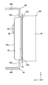
- FIG. 4 is a side view showing the structure of the semiconductor device
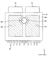
- FIG. 5 is a plan view showing the structure of the semiconductor device.
- the thickness direction of the lead frame is indicated as the Z direction
- the specific direction orthogonal to the Z direction is indicated as the X direction
- the direction orthogonal to the Z direction and the X direction is indicated as the Y direction.
- the semiconductor device 100 is connected to a current path through which current flows bidirectionally and forms a part of the current path.
- the semiconductor device 100 is applied to, for example, a power supply system including a lithium battery and a lead battery, and a system including an ISG and a lithium battery.
- ISG is an abbreviation for Integrated Starter Generator.
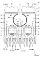
- the semiconductor device 100 includes a first chip 10, a second chip 20, and a shunt resistor 30.
- the semiconductor device 100 can also be referred to as a semiconductor module.
- the semiconductor device 100 includes a first terminal 100a, a second terminal 100b, control terminals 100c and 100d, and sense terminals 100e and 100f as terminals.
- the first chip 10 has a first switching element 12.
- the second chip 20 includes a second switching element 22.
- the switching elements 12 and 22 are elements for controlling whether or not current flows in the current path.
- the switching elements 12 and 22 are vertical semiconductor elements. In the present embodiment, the switching elements 12 and 22 are MOSFETs.
- the first switching element 12 has a parasitic diode.
- the parasitic diode has a cathode connected to the drain of the first switching element 12 and an anode connected to the source of the first switching element 12. Since the first switching element 12 is turned off, the path of the current flowing through the first switching element 12 is limited only to the path flowing from the anode to the cathode of the parasitic diode. That is, the 1st switching element 12 restrict
- the drain of the first switching element 12 is connected to the first terminal 100a.
- the first terminal 100a is connected to external wiring.
- the gate of the first switching element 12 is connected to the control terminal 100c.
- the source of the first switching element 12 is connected to one end of the shunt resistor 30.
- the first chip 10 may be formed with an element other than the first switching element 12 such as a temperature sensitive diode.
- the second switching element 22 has a parasitic diode.
- the parasitic diode has a cathode connected to the drain of the second switching element 22 and an anode connected to the source of the second switching element 22. Since the second switching element 22 is turned off, the path of the current flowing through the second switching element 22 is limited only to the path flowing from the anode to the cathode of the parasitic diode.
- the direction in which the parasitic diode current of the first switching element 12 flows in the current path formed by the semiconductor device 100 is opposite to the direction in which the parasitic diode current of the second switching element 22 flows.
- the second switching element 22 is turned off, thereby restricting a current from flowing in the direction opposite to the direction in which the first switching element 12 restricts the current in the current path.
- the drain of the second switching element 22 is connected to the second terminal 100b.
- the second terminal 100b is connected to external wiring.
- the gate of the second switching element 22 is connected to the control terminal 100d.
- the source of the second switching element 22 is connected to the other end of the shunt resistor 30 opposite to the one end connected to the first switching element 12. Note that elements other than the second switching element 22 such as a temperature-sensitive diode may be formed on the second chip 20.
- the shunt resistor 30 electrically relays the first switching element 12 and the second switching element 22 to form a part of the current path.
- the shunt resistor 30 corresponds to a wiring.
- the shunt resistor 30 has a resistor 32 for detecting the current flowing in the current path.
- a connection point between the source of the first switching element 12 and the shunt resistor 30 is connected to the sense terminal 100e.
- the connection point between the source of the second switching element 22 and the shunt resistor 30 is connected to the sense terminal 100f.
- the resistor 32 is disposed between the connection point of the first switching element 12 and the shunt resistor 30 and the connection point of the second switching element 22 and the shunt resistor 30. Therefore, the resistor 32 has one end connected to the sense terminal 100e and the other end connected to the sense terminal 100f. In other words, both ends of the resistor 32 are connected to the sense terminals 100e and 100f.
- the sense terminals 100e and 100f are connected to a current detection unit (not shown) that detects a current flowing through the current path.
- the sense terminals 100e and 100f output the voltage across the resistor 32 to the current detection unit.
- the voltage detection part can detect the voltage drop of the resistor 32, and can detect the value of the electric current which flows into a current path by extension.
- the control terminals 100c and 100d are connected to a control unit that controls the on / off state of the switching elements 12 and 22.
- the control unit controls the on / off states of the switching elements 12 and 22 by outputting a control signal to the control terminals 100c and 100d.
- the control unit determines whether or not current flows in the current path. More specifically, the control unit enables the current to flow in both directions with respect to the current path by turning on both of the switching elements 12 and 22. In addition, the control unit turns off both the switching elements 12 and 22 so that no current flows in both directions in the current path. More specifically, since the directions for limiting the current of the parasitic diodes of the switching elements 12 and 22 are opposite to each other, when both the switching elements 12 and 22 are turned off, the current path Current flow is limited. In other words, the control unit turns off both the switching elements 12 and 22 so that no current flows in the current path regardless of the direction of the current.
- the chips 10 and 20 have a rectangular shape in which each side is along the X direction or the Y direction. As shown in FIG. 3, the chips 10 and 20 have a flat plate shape whose thickness direction is along the Z direction.
- the first chip 10 has a front surface 10a and a back surface 10b which are flat surfaces perpendicular to the Z direction.
- a source electrode and a gate electrode of the first switching element 12 are formed on the surface 10a.
- a drain electrode of the first switching element 12 is formed on the back surface 10b.
- the second chip 20 has substantially the same shape as the first chip 10.
- the two chips 10 and 20 are arranged in the X direction.
- the second chip 20 has a front surface 20a and a back surface 20b which are flat surfaces orthogonal to the Z direction.
- a source electrode and a gate electrode of the second switching element 22 are formed on the surface 20a.
- a drain electrode of the second switching element 22 is formed on the back surface 20b.
- the second chip 20 is disposed at the same position as the first chip 10 in the Z direction. Specifically, in the Z direction, the position of the front surface 20a is equal to the position of the front surface 10a, and the position of the back surface 20b is equal to the position of the back surface 10b. The second chip 20 is disposed at the same position as the first chip 10 in the Y direction.
- the shunt resistor 30 has one end electrically and mechanically connected to the first chip 10 and the other end electrically and mechanically connected to the second chip 20. Thereby, the shunt resistor 30 functions as a wiring connecting the first chip 10 and the second chip 20.
- the shunt resistor 30 is formed extending in the X direction on the XY plane.
- the shunt resistor 30 is disposed on the surface 10 a side with respect to the first chip 10 and is disposed on the surface 20 a side with respect to the second chip 20.
- the resistance of the resistor 32 is larger than that of the portion other than the resistor 32.
- the resistor 32 is made of, for example, CuMnSn or CuMnNi as a main component. Portions other than the resistor 32 of the shunt resistor 30 are formed, for example, with copper as a main component.
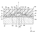
- the shunt resistor 30 includes fixed portions 34 a and 34 b fixed to the chips 10 and 20, a central portion 36 including the resistor 32, and a connection that connects the fixed portions 34 a and 34 b and the central portion 36. Parts 38a, 38b.
- the fixing part 34 a forms one end of the shunt resistor 30.
- the fixing portion 34a is soldered to the source electrode on the surface 10a.
- the fixed portion 34 b forms the other end opposite to the fixed portion 34 a of the shunt resistor 30.
- the fixing portion 34b is soldered to the source electrode on the back surface 10b.
- the electrodes formed on the surfaces 10a and 20a are plated so that they can be soldered.
- the fixing portions 34a and 34b have a flat plate shape whose thickness direction is along the Z direction. In the XY plane, the fixing portions 34a and 34b have a rectangular shape in which each side is along the X direction or the Y direction.
- the fixed portion 34a has a shorter width in the X direction and a width in the Y direction than the first chip 10.
- the fixing portion 34 b has a shorter width in the X direction and a width in the Y direction than the second chip 20.
- the entire fixing portion 34 a overlaps a part of the first chip 10.
- the entire fixing portion 34b overlaps a part of the second chip 20 in the projection view in the Z direction.
- the central portion 36 is disposed between the fixing portions 34a and 34b in the X direction. That is, the central portion 36 is disposed between the chips 10 and 20 in the X direction. The central portion 36 does not overlap the chips 10 and 20 in the projection view in the Z direction. Further, the central portion 36 is disposed on the surface 10a, 20a side with respect to the chips 10, 20 in the Z direction and at a position away from the surfaces 10a, 20a. That is, the central portion 36 is disposed at a position away from the fixing portions 34a and 34b in the Z direction.
- the central portion 36 has a flat plate shape whose thickness direction is along the Z direction. In the XY plane, the central portion 36 has a substantially rectangular shape with each side along the X direction or the Y direction. The width of the central portion 36 in the Y direction is longer than the width of the fixing portions 34a and 34b in the Y direction. The central portion 36 has a width in the Y direction that is substantially equal to that of the chips 10 and 20 and is disposed at a position that is substantially equal to the chips 10 and 20 in the Y direction.
- the resistor 32 is formed at the center of the central portion 36 in the X direction, and extends from one end to the other end of the central portion 36 in the Y direction.
- the connecting portion 38a is disposed between the fixed portion 34a and the central portion 36 in the X direction, and connects the fixed portion 34a and the central portion 36.
- the connecting portion 38b is disposed between the fixing portion 34b and the central portion 36 in the X direction, and connects the fixing portion 34b and the central portion 36. According to the above, in the X direction, the fixing portion 34a, the connecting portion 38a, the central portion 36, the connecting portion 38b, and the fixing portion 34b are arranged in this order.
- the connecting portions 38a and 38b have a rectangular shape on the XY plane.
- the connecting portions 38a and 38b have the same width in the Y direction as the fixed portions 34a and 34b, and are disposed at positions equal to the fixed portions 34a and 34b in the Y direction.
- the connecting portions 38a and 38b extend linearly with a predetermined angle with respect to the Z direction and the X direction.
- a part of the connecting portion 38 a overlaps a part of the first chip 10.
- a part of the connecting portion 38b overlaps a part of the second chip 20 in the projection view in the Z direction.
- the semiconductor device 100 further includes a lead frame 40, a bonding wire 50, a molding resin 60, an insulating sheet 70, a heat sink 80, and a screw 90 in addition to the first chip 10, the second chip 20, and the shunt resistor 30. ing.
- the screw 90 is omitted.
- the insulating sheet 70, the heat sink 80, and the screw 90 are omitted.
- the lead frame 40 forms a current path while fixing the chips 10 and 20.
- the lead frame 40 is formed using a metal material.
- the lead frame 40 includes a first lead 42, a second lead 44, and a plurality of pins 46.
- the first chip 10 is fixedly disposed on the first lead 42 and external wiring is connected thereto.
- the first lead 42 corresponds to the first terminal 100 a of the semiconductor device 100 and forms a current path.
- the first lead 42 is formed by bending a metal plate. More specifically, the first lead 42 has a flat plate portion 42a whose thickness direction is along the Z direction, and a flat plate portion 42b whose thickness direction is along the Y direction.
- the flat plate portion 42a is a portion to which the first chip 10 is fixed.
- the flat plate portion 42a has a front surface 42c and a back surface 42d opposite to the front surface 42c in the Z direction.
- the front surface 42c and the back surface 42d are planes orthogonal to the Z direction.
- the first chip 10 is disposed on the surface 42c.
- the first lead 42 is mechanically and electrically connected to the first chip 10 by soldering the front surface 42c to the back surface 10b. Thereby, the first lead 42 is connected to the drain electrode of the first switching element 12.
- the flat plate portion 42 a overlaps the first chip 10, the fixed portion 34 a, the connecting portion 38 a, and a part of the central portion 36.
- the flat plate portion 42b is a portion connected to external wiring.
- the flat plate portion 42b is connected to one end in the Y direction of the flat plate portion 42a.
- the flat plate portion 42b is bent from the flat plate portion 42a to the first chip 10 side in the Z direction.
- the second chip 20 is fixedly disposed on the second lead 44 and external wiring is connected thereto.
- the second lead 44 corresponds to the second terminal 100 b of the semiconductor device 100 and forms a current path.
- the second lead 44 has a symmetrical shape with the first lead 42 with respect to the symmetry plane S orthogonal to the X direction. That is, the second lead 44 has a shape that is plane-symmetric with respect to the first lead 42. Therefore, as shown in FIGS. 2 and 4, the second lead 44 is formed by bending the metal plate. 2 and 3, the symmetry plane S is indicated by a two-dot chain line.
- the symmetry plane S passes through the center of the shunt resistor 30 in the X direction.
- the shunt resistor 30 has a symmetrical shape with respect to the symmetry plane S.
- the first chip 10 is disposed at a position symmetrical to the second chip 20 with respect to the symmetry plane S.
- the second lead 44 has a flat plate portion 44a whose thickness direction is along the Z direction and a flat plate portion 44b whose thickness direction is along the Y direction.
- the flat plate portion 44a has a front surface 44c and a back surface 44d opposite to the front surface 42c in the Z direction.
- the front surface 44c and the back surface 42d are planes orthogonal to the Z direction.
- the second chip 20 is disposed on the surface 44c.
- the second lead 44 is mechanically and electrically connected to the second chip 20 by soldering the front surface 44c to the back surface 10b. Thereby, the second lead 44 is connected to the drain electrode of the second switching element 22.
- the second lead 44 is disposed at the same position as the first lead 42 in the Z direction. Specifically, in the Z direction, the position of the front surface 44c is equal to the position of the front surface 42c, and the position of the back surface 44d is equal to the position of the back surface 42d. Thereby, the positions of the chips 10 and 20 in the Z direction are made equal.
- the flat plate portion 44a overlaps with the second chip 20, the fixing portion 34b, the connecting portion 38b, and a part of the central portion 36.
- the flat plate portion 44b is connected to one end of the flat plate portion 44a in the Y direction.
- the flat plate portion 44b is bent from the flat plate portion 44a to the second chip 20 side in the Z direction.
- the flat plate portion 42a and the flat plate portion 42b are formed with holes 40a through which the screws 90 pass.
- the hole 40a has a substantially perfect circle shape in the XY plane.
- the hole 40a is formed by a region between the flat plate portion 42a and the flat plate portion 44a in the X direction.
- the flat plate portion 42a has a side surface facing the flat plate portion 44a that is recessed in a semicircular shape in the X direction.
- the flat plate portion 44b has a side surface facing the flat plate portion 42a that is recessed in a semicircular shape in the X direction.
- a hole 40a is formed by a recess in the side surfaces of the flat plate portions 42a and 44a.
- the hole 40 a is formed at a position that does not overlap the first chip 10, the second chip 20, and the shunt resistor 30.
- the hole 40a is formed on one side in the Y direction with respect to the central portion 36 in the projection view in the Z direction.
- the center of the hole 40a in the XY plane is indicated as a center C.
- a symmetry plane S that is a reference for plane symmetry of the leads 42 and 44 passes through the center C.
- the position of the symmetry plane S is made equal to the position of the center C in the X direction.
- the shortest distance from the center C of the hole 40a to the first chip 10 is equal to the shortest distance from the center C to the second chip 20.
- through holes 42e and 44e penetrating in the Z direction are formed.
- the connection strength between the lead frame 40 and the mold resin 60 is improved.
- grooves are formed in the periphery of the hole 40a on the surfaces 42c and 44c and in the vicinity of the openings of the through holes 42e and 44e.
- the leads 42 and 44 have protrusions 42f and 44f that protrude from both end surfaces in the X direction. Due to the anchor effect by the protrusions 42f and 44f, the connection strength between the lead frame 40 and the mold resin 60 is improved.
- the pin 46 is connected to the first chip 10, the second chip 20 or the shunt resistor 30 via the bonding wire 50, and the other end is connected to an external wiring.
- the lead frame 40 has nine pins 46. The number of pins 46 is not limited to nine.
- the pin 46 is opposite to the flat plate portion 42b in the Y direction of the first lead 42, opposite to the flat plate portion 44b in the Y direction of the second lead 44, and opposite to the hole 40a in the Y direction of the central portion 36. Has been placed.
- the nine pins 46 are arranged in the X direction.
- the pin 46 has a bent bar shape, and has a column part 46a extending in the Y direction and a column part 46b extending in the Z direction. One end of the column part 46 a is connected to the bonding wire 50.
- the column portion 46 a is connected to the column portion 46 b at the other end opposite to one end connected to the bonding wire 50.
- the column part 46b extends from the column part 46a in the same direction as the direction in which the flat plate part 42b extends from the flat plate part 42a in the Z direction.
- the column part 46b is connected to external wiring.
- the three pins 46 are electrically and mechanically connected to the first chip 10 via the bonding wires 50.
- the bonding wire 50 that electrically relays the pin 46 and the first chip 10 has one end connected to the column part 46 a and the other end connected to an electrode formed on the surface 10 a of the first chip 10.
- One of the three pins 46 connected to the first chip 10 corresponds to the control terminal 100c and is connected to the gate of the first switching element 12.
- the pin 46 corresponding to the control terminal 100c is connected to the control unit that controls the on / off state of the first switching element 12 by the column part 46b.
- the control unit transmits a control signal to the gate of the first switching element 12 through the pin 46 and the bonding wire 50.
- the remaining two pins 46 are connected to elements other than the first switching element 12 formed in the first chip 10.
- the four pins 46 are electrically and mechanically connected to the second chip 20 via the bonding wires 50.
- the bonding wire 50 that electrically relays the pin 46 and the second chip 20 has one end connected to the column part 46 a and the other end connected to an electrode formed on the surface 20 a of the second chip 20.
- One of the four pins 46 connected to the second chip 20 corresponds to the control terminal 100d and is connected to the gate of the second switching element 22.
- the pin 46 corresponding to the control terminal 100d is connected to the control unit by the pillar 46b.
- the control unit transmits a control signal to the gate of the second switching element 22 through the pin 46 and the bonding wire 50.
- the remaining three pins 46 are connected to elements other than the second switching element 22 formed in the second chip 20.
- the two pins 46 correspond to the sense terminals 100e and 100f, and are electrically and mechanically connected to the shunt resistor 30 via the bonding wires 50.
- One of the two pins 46 is connected to one end side of the resistor 32 through the bonding wire 50, and the other is connected to the other end side of the resistor 32 through the bonding wire 50.
- the bonding wire 50 connected to the shunt resistor 30 is connected to a portion of the central portion 36 other than the resistor 32 and close to the central portion 36.
- the pins 46 corresponding to the sense terminals 100e and 100f are connected to the current detection part by the pillar part 46b.
- the current detection unit detects the voltage across the resistor 32 via the bonding wire 50 and the pin 46.
- solder for connecting the leads 42 and 44 and the chips 10 and 20 and the solder for connecting the chips 10 and 20 and the shunt resistor 30 solder that does not leave a flex residue after heating is employed. According to this, it can suppress that the connection of the bonding wire 50 is inhibited by the flux residue.
- the mold resin 60 integrally seals the first chip 10, the second chip 20, the shunt resistor 30, and the lead frame 40. Thereby, the mold resin 60 holds the first chip 10, the second chip 20, the shunt resistor 30, and the lead frame 40.
- the mold resin 60 has one surface 60a orthogonal to the Z direction and a bottom surface 60b opposite to the one surface 60a in the Z direction.
- the one surface 60a is located on the opposite side of the chips 10 and 20 from the shunt resistor 30 in the Z direction and at a position away from the shunt resistor 30.
- the mold resin 60 has a symmetrical shape with respect to the symmetry plane S.
- the bottom surface 60b is in the same position as the back surfaces 42d and 44d in the Z direction, or slightly away from the one surface 60a than the back surfaces 42d and 44d. Thereby, as shown in FIGS. 3 and 5, the back surfaces 42 d and 44 d are exposed from the mold resin 60. In FIG. 5, in order to clarify the shapes of the back surfaces 42d and 44d, the back surfaces 42d and 44d are hatched.
- the first lead 42 has a part of the flat plate portion 42 a and the entire flat plate portion 42 b exposed from the mold resin 60. Thereby, the flat plate part 42b becomes connectable with an external wiring.
- the second lead 44 a part of the flat plate portion 44 a and the entire flat plate portion 44 b are exposed from the mold resin 60. Thereby, the flat plate portion 44b can be connected to the external wiring.
- the pin 46 a part of the column part 46 a and the entire column part 46 b are exposed from the mold resin 60. Thereby, the column part 46b becomes connectable with an external wiring.
- a through hole 60c through which the screw 90 passes is formed.
- the through hole 60c penetrates the mold resin 60 in the Z direction. In the XY plane, the diameter of the through hole 60c is smaller than the diameter of the hole 40a.
- the insulating sheet 70 is formed using an electrically insulating material.
- the insulating sheet 70 is interposed between the lead frame 40 and the heat sink 80 and electrically insulates the lead frame 40 and the heat sink 80.
- the insulating sheet 70 has a flat plate shape whose thickness direction is along the Z direction.
- the insulating sheet 70 is disposed in contact with the back surface 42d, the back surface 44d, and the bottom surface 60b.
- the insulating sheet 70 has a symmetrical shape with respect to the symmetry plane S.
- a through hole through which the screw 90 passes is formed in the insulating sheet 70.
- the through hole of the insulating sheet 70 extends in the Z direction and communicates with the through hole 60 c of the mold resin 60.
- a heat sink 80 is disposed on the side of the insulating sheet 70 opposite to the lead frame 40 and the mold resin 60.
- the heat sink 80 radiates the heat of the chips 10 and 20 to the outside.
- the heat sink 80 is formed using a metal material.
- the heat sink 80 has a cubic shape in which each side is along the X direction, the Y direction, or the Z direction.
- the heat sink 80 has a contact surface 80 a with the insulating sheet 70.
- the contact surface 80a is a plane orthogonal to the Z direction.
- the heat sink 80 is formed with a screw hole to be fastened with the screw 90.
- the screw hole of the heat sink 80 is formed with a predetermined depth in the Z direction from the contact surface 80a.
- the screw hole of the heat sink 80 communicates with the through hole 60 c of the mold resin 60 and the through hole of the insulating sheet 70.
- the heat sink 80 has a symmetrical shape with respect to the symmetry plane S.
- the screw 90 fixes the mold resin 60, the insulating sheet 70, and the heat sink 80 to each other.
- the screw 90 is fastened to the screw hole of the heat sink 80 through the through hole 60 c of the mold resin 60 and the through hole of the insulating sheet 70.
- the head of the screw 90 is disposed on one surface 60 a of the mold resin 60 via a washer 92.
- the screw 90 presses the lead frame 40 and the mold resin 60 against the insulating sheet 70 and the heat sink 80 side. Thereby, no gap is formed between the lead frame 40 and the mold resin 60 and the insulating sheet 70. Further, no gap is formed between the insulating sheet 70 and the heat sink 80.
- the chips 10 and 20 are connected to each other by a shunt resistor 30 for detecting a current flowing in the current path.
- the wiring can be omitted as compared with the configuration in which the shunt resistor 30 is provided separately from the wiring connecting the chips 10 and 20. Therefore, an increase in the number of parts of the semiconductor device 100 can be suppressed.
- the back surfaces 42d and 44d of the leads 42 and 44 are exposed from the mold resin 60. According to this, compared with the configuration in which the back surfaces 42d and 44d are covered with the mold resin 60, the heat of the chips 10 and 20 is easily radiated from the back surfaces 42d and 44d. Therefore, it is possible to effectively suppress the chips 10 and 20 from becoming high temperature.
- the leads 42 and 44 have a symmetrical shape with respect to a symmetry plane S orthogonal to the arrangement direction of the chips 10 and 20. That is, the shape of the first lead 42 that is the heat dissipation path of the first chip 10 is symmetrical to the second lead 44 that is the heat dissipation path of the second chip 20. According to this, the heat radiation amount from the first chip 10 to the first lead 42 can be close to the heat radiation amount from the second chip 20 to the second lead 44. Therefore, it can suppress that one of the chips 10 and 20 becomes high temperature compared with the other.
- the heat sink 80 radiates the heat of the chips 10 and 20 while the insulating sheet 70 electrically insulates the lead frame 40 and the heat sink 80. According to this, as compared with a configuration in which the semiconductor device 100 does not include the insulating sheet 70 and the heat sink 80, it is possible to effectively suppress the chips 10 and 20 from becoming high temperature.
- the lead frame 40, the insulating sheet 70, and the heat sink 80 may be fixed to each other via an adhesive.
- the heat of the chips 10 and 20 passes through the adhesive as a heat transfer path.
- the lead frame 40, the insulating sheet 70, and the heat sink 80 are screwed together. According to this, the heat of the chips 10 and 20 is directly transmitted from the leads 42 and 44 to the insulating sheet 70 and also directly transmitted from the insulating sheet 70 to the heat sink 80. Therefore, the heat of the chips 10 and 20 is easily transmitted to the heat sink 80, and it is possible to effectively suppress the chips 10 and 20 from becoming high temperature.
- the portion of the leads 42 and 44 closer to the hole 40a through which the screw 90 passes is more likely to conduct heat to the heat sink 80.
- tips 10 and 20 is made mutually equal in XY plane.
- the symmetry plane S which is a reference for plane symmetry between the leads 42 and 44, passes through the center C of the hole 40a.
- the shape of the portion of the first lead 42 that easily radiates heat to the heat sink 80 is symmetrical to the portion of the second lead 44 that easily radiates heat to the heat sink 80. Therefore, the heat radiation amounts from the chips 10 and 20 to the leads 42 and 44 can be made close to each other, and one of the chips 10 and 20 can be effectively suppressed from becoming higher temperature than the other.
- the semiconductor device 100 includes the insulating sheet 70 and the heat sink 80 has been described, but the present invention is not limited to this.
- the back surfaces 42 d and 44 d of the leads 42 and 44 exposed from the mold resin 60 may be in contact with the air around the semiconductor device 100.
- the switching elements 12 and 22 showed the example which is MOSFET, it is not limited to this.
- bipolar transistors and IGBTs can be employed as the switching elements 12 and 22.
- the switching elements 12 and 22 may be elements different from each other.
Landscapes
- Engineering & Computer Science (AREA)
- Microelectronics & Electronic Packaging (AREA)
- Power Engineering (AREA)
- Physics & Mathematics (AREA)
- General Physics & Mathematics (AREA)
- Computer Hardware Design (AREA)
- Condensed Matter Physics & Semiconductors (AREA)
- Inverter Devices (AREA)
- Measuring Instrument Details And Bridges, And Automatic Balancing Devices (AREA)
Priority Applications (2)
| Application Number | Priority Date | Filing Date | Title |
|---|---|---|---|
| CN201780060940.1A CN109791926A (zh) | 2016-10-07 | 2017-09-27 | 半导体装置 |
| US16/360,341 US10998295B2 (en) | 2016-10-07 | 2019-03-21 | Semiconductor device |
Applications Claiming Priority (2)
| Application Number | Priority Date | Filing Date | Title |
|---|---|---|---|
| JP2016199127A JP6645396B2 (ja) | 2016-10-07 | 2016-10-07 | 半導体装置 |
| JP2016-199127 | 2016-10-07 |
Related Child Applications (1)
| Application Number | Title | Priority Date | Filing Date |
|---|---|---|---|
| US16/360,341 Continuation US10998295B2 (en) | 2016-10-07 | 2019-03-21 | Semiconductor device |
Publications (1)
| Publication Number | Publication Date |
|---|---|
| WO2018066420A1 true WO2018066420A1 (ja) | 2018-04-12 |
Family
ID=61831648
Family Applications (1)
| Application Number | Title | Priority Date | Filing Date |
|---|---|---|---|
| PCT/JP2017/034829 Ceased WO2018066420A1 (ja) | 2016-10-07 | 2017-09-27 | 半導体装置 |
Country Status (4)
| Country | Link |
|---|---|
| US (1) | US10998295B2 (enExample) |
| JP (1) | JP6645396B2 (enExample) |
| CN (1) | CN109791926A (enExample) |
| WO (1) | WO2018066420A1 (enExample) |
Families Citing this family (8)
| Publication number | Priority date | Publication date | Assignee | Title |
|---|---|---|---|---|
| US11107761B2 (en) * | 2018-02-06 | 2021-08-31 | Denso Corporation | Semiconductor device |
| JP2019186403A (ja) | 2018-04-11 | 2019-10-24 | トヨタ自動車株式会社 | 半導体装置 |
| DE102018207308B4 (de) * | 2018-05-09 | 2020-07-02 | Infineon Technologies Ag | Halbleiterbauteil mit integriertem shunt-widerstand und verfahren zu dessen herstellung |
| JP2020047725A (ja) * | 2018-09-18 | 2020-03-26 | トヨタ自動車株式会社 | 半導体装置 |
| JP7338204B2 (ja) * | 2019-04-01 | 2023-09-05 | 富士電機株式会社 | 半導体装置 |
| JP7479759B2 (ja) * | 2020-06-02 | 2024-05-09 | 三菱電機株式会社 | 半導体装置の製造方法、および、半導体装置 |
| US11555832B2 (en) * | 2021-03-02 | 2023-01-17 | Allegro Microsystems, Llc | Integrated shunt and magnetic field current sensor |
| EP4443734A1 (en) * | 2023-04-06 | 2024-10-09 | Hamilton Sundstrand Corporation | Shoot-through protection and current monitoring scheme for multilevel power converters |
Citations (4)
| Publication number | Priority date | Publication date | Assignee | Title |
|---|---|---|---|---|
| JP2010267789A (ja) * | 2009-05-14 | 2010-11-25 | Renesas Electronics Corp | 半導体装置 |
| JP2011254387A (ja) * | 2010-06-03 | 2011-12-15 | Rohm Co Ltd | 交流スイッチ |
| US20150115313A1 (en) * | 2013-10-31 | 2015-04-30 | Infineon Technologies Austria Ag | Semiconductor Device Package |
| WO2016075985A1 (ja) * | 2014-11-13 | 2016-05-19 | 株式会社村田製作所 | パワー半導体のパッケージ素子 |
Family Cites Families (8)
| Publication number | Priority date | Publication date | Assignee | Title |
|---|---|---|---|---|
| JP2003199350A (ja) | 2001-12-27 | 2003-07-11 | Sanken Electric Co Ltd | 3相交流‐直流変換装置 |
| JP4471967B2 (ja) * | 2006-12-28 | 2010-06-02 | 株式会社ルネサステクノロジ | 双方向スイッチモジュール |
| JP5592073B2 (ja) | 2009-02-09 | 2014-09-17 | 富士電機株式会社 | 双方向スイッチの電流検出回路 |
| JP5477669B2 (ja) * | 2012-02-28 | 2014-04-23 | 株式会社デンソー | 半導体モジュール |
| CN105745812A (zh) * | 2013-12-27 | 2016-07-06 | 英特尔公司 | 用于电子设备的功率递送系统 |
| JP6384112B2 (ja) * | 2014-04-25 | 2018-09-05 | 三菱マテリアル株式会社 | パワーモジュール用基板及びヒートシンク付パワーモジュール用基板 |
| JP6384211B2 (ja) * | 2014-09-03 | 2018-09-05 | 株式会社デンソー | シャント抵抗器 |
| US9979187B2 (en) * | 2015-11-12 | 2018-05-22 | Infineon Technologies Austria Ag | Power device with overvoltage arrester |
-
2016
- 2016-10-07 JP JP2016199127A patent/JP6645396B2/ja active Active
-
2017
- 2017-09-27 WO PCT/JP2017/034829 patent/WO2018066420A1/ja not_active Ceased
- 2017-09-27 CN CN201780060940.1A patent/CN109791926A/zh active Pending
-
2019
- 2019-03-21 US US16/360,341 patent/US10998295B2/en active Active
Patent Citations (4)
| Publication number | Priority date | Publication date | Assignee | Title |
|---|---|---|---|---|
| JP2010267789A (ja) * | 2009-05-14 | 2010-11-25 | Renesas Electronics Corp | 半導体装置 |
| JP2011254387A (ja) * | 2010-06-03 | 2011-12-15 | Rohm Co Ltd | 交流スイッチ |
| US20150115313A1 (en) * | 2013-10-31 | 2015-04-30 | Infineon Technologies Austria Ag | Semiconductor Device Package |
| WO2016075985A1 (ja) * | 2014-11-13 | 2016-05-19 | 株式会社村田製作所 | パワー半導体のパッケージ素子 |
Also Published As
| Publication number | Publication date |
|---|---|
| US10998295B2 (en) | 2021-05-04 |
| US20190221549A1 (en) | 2019-07-18 |
| JP2018060966A (ja) | 2018-04-12 |
| CN109791926A (zh) | 2019-05-21 |
| JP6645396B2 (ja) | 2020-02-14 |
Similar Documents
| Publication | Publication Date | Title |
|---|---|---|
| JP6645396B2 (ja) | 半導体装置 | |
| US11075190B2 (en) | Semiconductor device and semiconductor device fabrication method | |
| US10861756B2 (en) | Semiconductor device including sensor and driving terminals spaced away from the semiconductor device case wall | |
| US7247929B2 (en) | Molded semiconductor device with heat conducting members | |
| CN114175234B (zh) | 半导体装置及电子装置 | |
| US8749977B2 (en) | Power semiconductor module and its attachment structure | |
| CN103314437B (zh) | 功率半导体模块及电源单元装置 | |
| JP4985810B2 (ja) | 半導体装置 | |
| US20160225690A1 (en) | Semiconductor device | |
| CN107492531B (zh) | 半导体装置 | |
| CN110771027B (zh) | 功率半导体装置及使用该装置的电力转换装置 | |
| US11177190B2 (en) | Semiconductor device | |
| CN110176446B (zh) | 半导体装置 | |
| US11315850B2 (en) | Semiconductor device | |
| US9202766B2 (en) | Package for power device and method of making the same | |
| CN110582847B (zh) | 半导体模块 | |
| US10109603B2 (en) | Semiconductor device | |
| WO2020153190A1 (ja) | 半導体モジュールおよびac/dcコンバータユニット | |
| JP4403166B2 (ja) | パワーモジュールおよび電力変換装置 | |
| JP7626293B2 (ja) | 半導体モジュール、半導体装置、及び半導体装置の製造方法 | |
| JP2013207168A (ja) | 半導体モジュール | |
| WO2024122399A1 (ja) | 半導体装置 | |
| JPH11163240A (ja) | 半導体スイッチの電極構造 | |
| JP2011066282A (ja) | 発熱デバイス装置 |
Legal Events
| Date | Code | Title | Description |
|---|---|---|---|
| 121 | Ep: the epo has been informed by wipo that ep was designated in this application |
Ref document number: 17858258 Country of ref document: EP Kind code of ref document: A1 |
|
| NENP | Non-entry into the national phase |
Ref country code: DE |
|
| 122 | Ep: pct application non-entry in european phase |
Ref document number: 17858258 Country of ref document: EP Kind code of ref document: A1 |